sps -43 -48h -hp -tde - source photonics · receiver cid tolerance 72 - - bits table 6 – receiver...
TRANSCRIPT
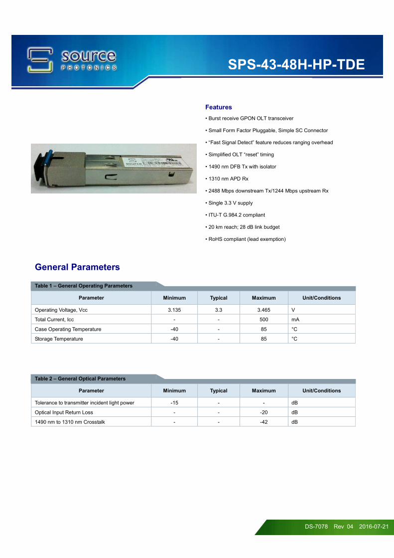
SPS-43-48H-HP-TDE
DS-7078 Rev 04 2016-07-21
General Parameters
Table 1 – General Operating Parameters
Parameter Minimum Typical Maximum Unit/Conditions
Operating Voltage, Vcc 3.135 3.3 3.465 V
Total Current, Icc - - 500 mA
Case Operating Temperature -40 - 85 °C
Storage Temperature -40 - 85 °C
Table 2 – General Optical Parameters
Parameter Minimum Typical Maximum Unit/Conditions
Tolerance to transmitter incident light power -15 - - dB
Optical Input Return Loss - - -20 dB
1490 nm to 1310 nm Crosstalk - - -42 dB
Features
• Burst receive GPON OLT transceiver
• Small Form Factor Pluggable, Simple SC Connector
• “Fast Signal Detect” feature reduces ranging overhead
• Simplified OLT “reset” timing
• 1490 nm DFB Tx with isolator
• 1310 nm APD Rx
• 2488 Mbps downstream Tx/1244 Mbps upstream Rx
• Single 3.3 V supply
• ITU-T G.984.2 compliant
• 20 km reach; 28 dB link budget
• RoHS compliant (lead exemption)
SPS-43-48H-HP-TDE
DS-7078 Rev 04 2016-07-21
Functional Characteristics
The following tables list the performance specifications for the various functional blocks of the integrated optical transceiver module.
Table 3 – Transmitter Specifications (Optical)
Parameter Minimum Typical Maximum Unit Notes
Average Optical Output Power, Po 1.5 - 5 dBm
Output Power at Transmit Off - - -40 dBm
Center Wavelength, λ 1480 1490 1500 nm
-20 dB Spectral Width - - 1 nm
Side Mode Suppression Ratio (SMSR) 30 - - dB
Extinction Ratio 8.2 - - dB PRBS 223-1, NRZ, 50% duty cycle
Transmitter Output Eye G.984.2 Figure 2
Optical Rise and Fall Time - - 250 ps 20% to 80%
Bit Rate - 2488 - Mbps
Table 4 – Transmitter Specifications (Electrical)
Parameter Minimum Typical Maximum Unit Notes
Input Differential Impedance 80 100 120 Ω
Differential Input Voltage Swing 200 - 2400 mV
Tx Disable (LVTTL) 2 - Vcc V
Tx Enable (LVTTL) 0 - 0.8 V
TX_Fail_High 2 - Vcc V
TX_Fail_Normal 0 - 0.4 V
Table 5 – Receiver Specifications (Optical)
Parameter Minimum Typical Maximum Unit Notes
Operational Wavelength Range 1260 1310 1360 nm
Data Rate (burst mode) - 1244 - Mbps
Receiver Burst-Mode Sensitivity - - -28 dBm At 10-10 BER, PRBS 223-1, 20km fiber
Receiver Overload -8 - - dBm
Burst Detect Assert - - -30 dBm
Burst_Detect De-Assertion -45 dBm
Receiver Burst Mode Dynamic Range 15 - - dB Input power difference between two
subsequent high and low burst data
SPS-43-48H-HP-TDE
DS-7078 Rev 04 2016-07-21
Parameter Minimum Typical Maximum Unit Notes
Receiver CID Tolerance 72 - - bits
Table 6 – Receiver Specifications (Electrical)
Parameter Minimum Typical Maximum Unit Notes
Differential Output Voltage Swing - 1500 - mV
Data Output Rise Time - - 300 ps 20% to 80%
Data Output Fall Time - - 300 ps 20% to 80%
Signal Detect Output HIGH 2.4 - Vcc V
Signal Detect Output LOWa 0 - 0.4 V
Signal Detect Assert Time - - 100 ns
Signal Detect De-assert Time - - 12.8 ns
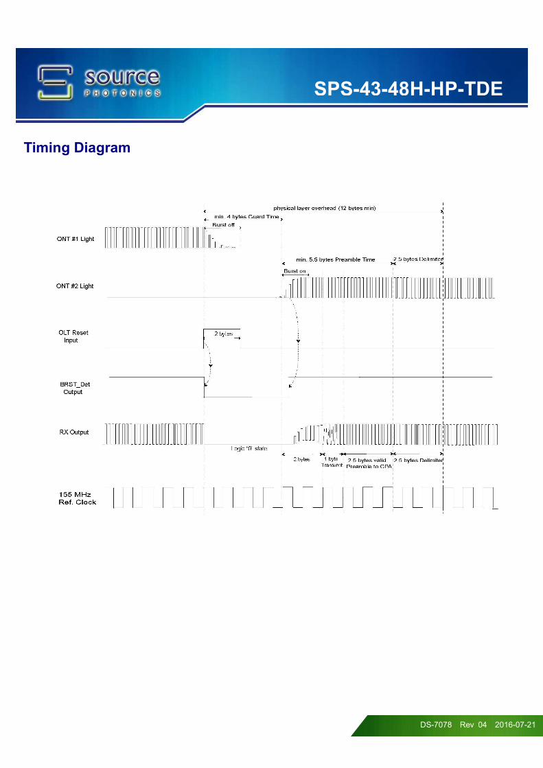
a) Signal Detect assert low when module receive “reset” signal, assert high when incoming burst is detected and latch to high state until next “Reset”
signal.
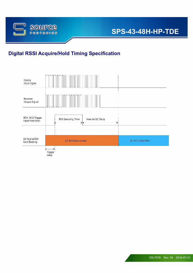
Table 7 – Digital RSSI Timing Specification
Parameter Minimum Typical Maximum Unit Notes
Data recovery time - - 50 ns
RSSI Sampling Timea 300 - - ns
Internal I2C Delaya - - 500 us
Receiver Power DDM (RSSI) Errorb - - +/- 3 dB
a) RSSI_ACQ input signal rising edge will trigger RSSI sampling, and falling edge will trigger internal digital RSSI information written to I2C.
It is recommended that host shall not trigger RSSI_ACQ input again until RSSI data is valid in I2C from previous RSSI trigger.
b) RSSI DDM working range is between -10 to -30 dBm. RSSI DDM accuracy reduces to +/- 5 dB for -10 to -8dBm.
SPS-43-48H-HP-TDE
DS-7078 Rev 04 2016-07-21
Pin Definitions
Refer to Table 8 for a description of the function of each I/O pin.
Table 8 - Module Pin Definitions
Pin Number Label Definition
1 Veet Tx Ground
2 Tx_Fail
(Tx_Fault) Tx Fail Alarm. LVTTL Output Active High
3 Tx_DIS Tx Disable. LVTTL input. Laser output is disabled when this pin is asserted high or left
unconnected. Laser output is enabled when this pin is asserted low.
4 MOD_DEF (2) 2-Wire Serial Data I/O Pin.
5 MOD_DEF (1) 2-Wire Serial Clock Input.
6 MOD_DEF (0) Internally Grounded
7 Reset CMOS input. Assert “Reset” high at the end of previous burst, 2 bytes in duration
8 BRST_Det LVTTL output. BRST_Det assert low when module receives “reset” signal, assert high
when incoming burst is present.
9 RSSI_ACQ RSSI acquire/hold LVTTL Input. Digital RSSI output through I2C
10 Veer Rx Ground
11 Veer Rx Ground
12 RXD- Negative Data Output, LVPECL; DC coupled
13 RXD+ Positive Data Output, LVPECL; DC coupled
14 Veer Rx Ground
15 Vcc_Rx Rx Vcc
16 Vcc_Tx Tx Vcc
17 Veet Tx Ground
18 TXD+ Positive Data Input, LVPECL or CML (AC coupled; internally 100 ohms differential
termination)
19 TXD- Negative Data Input, LVPECLor CML (AC coupled; internally 100 ohms differential
termination)
20 Veet Tx Ground
SPS-43-48H-HP-TDE
DS-7078 Rev 04 2016-07-21
Timing Diagram
SPS-43-48H-HP-TDE
DS-7078 Rev 04 2016-07-21
Digital RSSI Acquire/Hold Timing Specification
SPS-43-48H-HP-TDE
DS-7078 Rev 04 2016-07-21
EEPROM Content
Table 9 –EEPROM Content A0h
DEC
Addr.
HEX
Addr.
Field Size
(bytes) Name Default Value Description
0 00 1 Identifier 03h SFP Transceiver
1 01 1 Extended Identifier 04h Function defined by serial
ID
2 02 1 Connector 01h SC Receptacle
3 03 8 Transceiver 00 00 00 00 00 00 00 00h Transceiver Code Field, not
applicable
11 0B 1 Encoding 03h NRZ encoding
12 0C 1 Nominal Bit Rate in 100
MBps 19h 2488.32 Mbps
13 0D 1 Reserved 00h Reserved
14 0E 1 Length (9µ,km) in km 14h 20km
15 0F 1 Length (9µ,m) in 100m C8h 20km
16 10 1 Length (50µ) in 10m 00h Not Supported
17 11 1 Length (62.5µ) in 10m 00h Not Supported
18 12 1 Length (Copper) in m 00h Not Supported
19 13 1 Reserved 00h Reserved
20 14 16 Vendor Name (ASCII) "SOURCEPHOTONICS" Vendor Name (ASCII)
36 24 1 Reserved 00h Reserved
37 25 3 Vender IEEE Company
ID 00 06 B5h Source Photonics IEEE ID
40 28 16 Vendor Part Number
(ASCII) "SPS4348HHPTDE"
Vendor Part Number
(ASCII)
56 38 4 Vendor Rev (ASCII) 31 20 20 20h Revision 1
60 3C 2 Laser Wavelength in nm 05 D2h 1490nm Tx Wavelength
62 3E 1 Reserved 00h Reserved
63 3F 1 Check Code for Base ID
Fields xxh Checksum from byte 0-62
64 40 2 Options 00 1Ch TX_DIS, TX_Fault, SD
66 42 1 Upper Bit Rate Margin
in % 00h BR, Max not specified
67 43 1 Lower Bit Rate Margin
in % 00h BR, Min not specified
SPS-43-48H-HP-TDE
DS-7078 Rev 04 2016-07-21
68 44 16 Vendor Serial Number
(ASCII) "xxxxxxxxxxxxxxxx"
16 byte Serial number field
(ASCII)
84 54 8 Date Code xx xx xx xx xx xx 20 20h Year(2 bytes) month(2
bytes) day(2 bytes)
92 5C 1 Diagnostic Monitoring
Type 58h
Ext Calibration, Average
Power Measurement
93 5D 1 Enhanced Options E0h
Optical Alarm/warning
implemented Soft TX_DIS,
TX_FAULT implemented
94 5E 1 SFF-8472 Compliance 02h Compliance to SFF-8472
Rev 9.4
95 5F 1 Check Code for
Extended ID Fields xxh Checksum from byte 64-69
96 60 26 Vendor Specific “SPS-43-48H-HP-TDE” SP Part Number
126 7E 2 Vendor Specific 00 00h Reserved
128 80 128 Reserved 00….00h Reserved; return to 0
Note: The “xx” byte should be filled in according to practical case. For more information, please refer to the related document of
SFF-8472 Rev 9.5.
Table 10 – EEPROM Content A2h
DEC
Addr.
HEX
Addr.
Field Size
(bytes) Name Default Value Description
0 00 2 Temp High Alarm 5C 00h 92C
2 02 2 Temp Low Alarm D0 00h -48C
4 04 2 Temp High Warning 57 00h 87C
6 06 2 Temp Low Warning D5 00h -43C
8 08 2 Voltage High Alarm 94 70h 3.8V
10 0A 2 Voltage Low Alarm 6D 60h 2.8V
12 0C 2 Voltage High Warning 8C A0h 3.6V
14 0E 2 Voltage Low Warning 75 30h 3.0V
16 10 2 Bias High Alarm C3 50h 100mA
18 12 2 Bias Low Alarm 03 E8h 2mA
20 14 2 Bias High Warning AF C8h 90mA
22 16 2 Bias Low Warning 05 DCh 3mA
24 18 2 TX Power High Alarm C3 C6h +7.0 dBm
26 1A 2 TX Power Low Alarm 2B D4h +0.5 dBm
SPS-43-48H-HP-TDE
DS-7078 Rev 04 2016-07-21
28 1C 2 TX Power High Warning AE 7Ch +6.5 dBm
30 1E 2 TX Power Low Warning 31 2Dh +1.0 dBm
32 20 2 RX Power High Alarm FF FFh No alarm
34 22 2 RX Power Low Alarm 00 00h No alarm
36 24 2 RX Power High Warning FF FFh No alarm
38 26 2 RX Power Low Warning 00 00h No alarm
40 28 16 Reserved 00….000h Reserved
56 38 4 RX_PWR(4) Calibration xx xx xx xxh 4th order RSSI calibration coefficient
60 3C 4 RX_PWR(3) Calibration xx xx xx xxh 3rd order RSSI calibration coefficient
64 40 4 RX_PWR(2) Calibration xx xx xx xxh 2nd order RSSI calibration coefficient
68 44 4 RX_PWR(1) Calibration xx xx xx xxh 1st order RSSI calibration coefficient
72 48 4 RX_PWR(0) Calibration xx xx xx xxh 0th order RSSI calibration coefficient
76 4C 2 TX_I(Slope) Calibration xx xxh Slope for Bias calibration
78 4E 2 TX_I(Offset) Calibration 00 00h Offset for Bias calibration
80 50 2 TX_PWR(Slope)
Calibration xx xxh
Slope for TX Power calibration
82 52 2 TX_PWR(Offset)
Calibration xx xxh
Offset for TX Power calibration
84 54 2 T(Slope) Calibration 01 00h Slope for Temperature calibration
86 56 2 T(Offset) Calibration xx xxh Offset for Temperature calibration, in
units of 256ths C
88 58 2 V(Slope) Calibration 01 00h Slope for VCC calibration
90 5A 2 V(Offset) Calibration 00 00h Offset for VCC calibration
92 5C 3 Reserved 00h reserved
95 5F 1 Checksum xxh Checksum
96 60 2 Transceiver Temperature xx xxh Temperature in C/256
98 62 2 Supply Voltage xx xxh Vcc
100 64 2 TX Bias Current xx xxh BIASMON
102 66 2 TX Optical Output Power xx xxh Back facet monitor
104 68 2 RX Optical Input Power xx xxh RSSI
106 6A 2 Reserved 0000h Reserved
108 6C 2 Reserved 0000h Reserved
110
6E.7 1bit TX_DIS State x Digital state of the TX Disable Input
Pin.
6E.6 1bit Soft TX Disable x Read/write bit that allows software
disable of laser.
6E.5 1bit Reserved. 0 Reserved.
6E.4 1bit Rate Select State 0 NOT SUPPORTED.
SPS-43-48H-HP-TDE
DS-7078 Rev 04 2016-07-21
6E.3 1bit Rate Select 0 NOT SUPPORTED.
6E.2 1bit TX_FAULT x Digital state of the TX Fault Output Pin.
6E.1 1bit LOS 0 Digital state of the LOS Output Pin.
NOT SUPPORTED
6E.0 1bit Data_ready_bar x Indicates transceiver has achieved
power up and data is ready.
111
6F.7 1bit Reserved 0 Reserved
6F.6 1bit Reserved 0 Reserved
6F.5 1bit Reserved 0 Reserved
6F.4 1bit Reserved 0 Reserved
6F.3 1bit Reserved 0 Reserved
6F.2 1bit INTERRUPT_NOT x Interrupt state (active low)
6F.1 1bit MODE_EN 0 TX FAULT pin enable
6F.0 1bit APD_SHUTDOWN x APD shut-down latch. Write 0 to clear
condition
112
70.7 1bit Temperature too high
alarm x Temperature too high alarm
70.6 1bit Temperature too low
alarm x Temperature too low alarm
70.5 1bit VCC too high alarm x VCC too high alarm
70.4 1bit VCC too low alarm x VCC too low alarm
70.3 1bit BIASMON too high alarm x BIASMON too high alarm
70.2 1bit BIASMON too low alarm x BIASMON too low alarm
70.1 1bit BFMON too high alarm x BFMON too high alarm
70 1bit BFMON too low alarm x BFMON too low alarm
113
71.7 1bit RSSI too high alarm x RSSI too high alarm
71.6 1bit RSSI too low alarm x RSSI too low alarm
71.5 1bit Reserved interrupt status
bit x Reserved interrupt status bit
71.4 1bit Reserved interrupt status
bit x Reserved interrupt status bit
71.3 1bit Reserved interrupt status
bit x Reserved interrupt status bit
71.2 1bit Reserved interrupt status
bit x Reserved interrupt status bit
71.1 1bit Reserved interrupt status
bit x TX Fail went HIGH
71 1bit Reserved interrupt status x APD Shutdown event detected
SPS-43-48H-HP-TDE
DS-7078 Rev 04 2016-07-21
bit
114 72 1 Reserved 00h Interrupt Mask for ISRC0
115 73 1 Reserved 00h Interrupt Mask for ISRC1
116
74.7 1bit Temperature too high
warning x Temperature too high warning
74.6 1bit Temperature too low
warning x Temperature too low warning
74.5 1bit VCC too high warning x VCC too high warning
74.4 1bit VCC too low warning x VCC too low warning
74.3 1bit BIASMON too high
warning x BIASMON too high warning
74.2 1bit BIASMON too low
warning x BIASMON too low warning
74.1 1bit BFMON too high warning x BFMON too high warning
74 1bit BFMON too low warning x BFMON too low warning
117
75.7 1bit RX Power High Warning x RSSI too high warning
75.6 1bit RX Power Low Warning x RSSI too low warning
75.5 1bit Reserved 0 Reserved
75.4 1bit Reserved 0 Reserved
75.3 1bit Reserved 0 Reserved
75.2 1bit Reserved 0 Reserved
75.1 1bit Reserved 0 Reserved
75 1bit Reserved 0 Reserved
118 76 1 Reserved 00h Interrupt Mask for ISRC2
119 77 1 Reserved 00h Interrupt Mask for ISRC3
120 78 8 Vendor Specific 00 00 00 00
00 00 00 00h Vendor Specific
SPS-43-48H-HP-TDE
DS-7078 Rev 04 2016-07-21
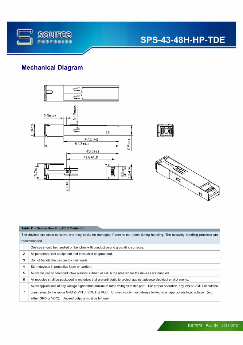
Mechanical Diagram
Table 11 - Device Handling/ESD Protection
The devices are static sensitive and may easily be damaged if care is not taken during handling. The following handling practices are
recommended.
1 Devices should be handled on benches with conductive and grounding surfaces.
2 All personnel, test equipment and tools shall be grounded.
3 Do not handle the devices by their leads.
4 Store devices in protective foam or carriers.
5 Avoid the use of non-conductive plastics, rubber, or silk in the area where the devices are handled
6 All modules shall be packaged in materials that are anti-static to protect against adverse electrical environments.
7
Avoid applications of any voltage higher than maximum rated voltages to this part. For proper operation, any VIN or VOUT should be
constrained to the range GND ≤ (VIN or VOUT) ≤ VCC. Unused inputs must always be tied to an appropriate logic voltage (e.g.
either GND or VCC). Unused outputs must be left open.
SPS-43-48H-HP-TDE
DS-7078 Rev 04 2016-07-21
Warnings
Handling Precautions: This device is susceptible to damage as a result of electrostatic discharge (ESD). A static free environment is highly
recommended. Follow guidelines according to proper ESD procedures.
Laser Safety: Radiation emitted by laser devices can be dangerous to human eyes. Avoid eye exposure to direct or indirect radiation.
Legal Notice
IMPORTANT NOTICE!
All information contained in this document is subject to change without notice, at Source Photonics’ sole and absolute discretion. Source Photonics
warrants performance of its products to current specifications only in accordance with the company’s standard one-year warranty; however, specifications
designated as “preliminary” are given to describe components only, and Source Photonics expressly disclaims any and all warranties for said products,
including express, implied, and statutory warranties, warranties of merchantability, fitness for a particular purpose, and non-infringement of proprietary
rights. Please refer to the company’s Terms and Conditions of Sale for further warranty information.
Source Photonics assumes no liability for applications assistance, customer product design, software performance, or infringement of patents, services,
or intellectual property described herein. No license, either express or implied, is granted under any patent right, copyright, or intellectual property right,
and Source Photonics makes no representations or warranties that the product(s) described herein are free from patent, copyright, or intellectual property
rights. Products described in this document are NOT intended for use in implantation or other life support applications where malfunction may result in
injury or death to persons. Source Photonics customers using or selling products for use in such applications do so at their own risk and agree to fully
defend and indemnify Source Photonics for any damages resulting from such use or sale.
© Copyright Source Photonics, Inc. 2007~2016
All Rights Reserved.
All information contained in this document is subject to change without notice. The products described in this document are NOT
intended for use in implantation or other life support applications where malfunction may result in injury or death to persons.
The information contained in this document does not affect or change Source Photonics product specifications or warranties. Nothing in
this document shall operate as an express or implied license or indemnity under the intellectual property rights of Source Photonics or
third parties. All information contained in this document was obtained in specific environments, and is presented as an illustration. The
results obtained in other operating environments may vary.
THE INFORMATION CONTAINED IN THIS DOCUMENT IS PROVIDED ON AN ”AS IS” BASIS. In no event will Source Photonics be
liable for damages arising directly from any use of the information contained in this document.
Contact
SOURCE PHOTONICS
20550 NORDHOFF ST.
CHATSWORTH, CA 91311
Tel: 818-773-9044 Fax: 818-576-9486
Or visit our website: http://www.sourcephotonics.com