statcom model paper
TRANSCRIPT

5/8/2018 Statcom Model Paper - slidepdf.com
http://slidepdf.com/reader/full/statcom-model-paper-559bf4e1099d4 1/5
Hoang Le-Huy/
2 Dept. of Electrical and Computer Engineering
Universite LavalQuebec, QC, Canada
lehuy@gel ulaval ca
IECONtO!; The 27th Annual Con fe re nc e o f th e IEEE Industria l E lectron ics Society
Modeling and Simulation of a Distribution STATCOM
using Simulink's Power System Blockset
Pierre Giroux 1 Gilbert Sybille!
Laboratoire Simulation de reseaux
Institut de recherche d'Hydro-Quebec (IREQ)
Varennes, QC, Canada
giroux [email protected], sybille [email protected]
Abstract - Ihis paper presents a study on the modeling ofa SIAl··
COM (Static Synchronous Compensator) used foI'reactive power
compensation on a distribution network, The power circuits ofthe
D-STATCOM and the distribution network are modeled by spe-
cific blocks (rom the Power System Blockset while the control sys-
tem i s modeled by Simulink blocks. Static and dynamic
performance of a ±3 Mvar D,Sl>1:ICQM on a 25-kV network is
evaluated, An "average modeling" approach is proposed to sim-
plify the PWM inverter operation and to accelerate the simulation
for control parameters adjusting purpose, Simulation perfor-mance obtained with both modeling approaches are presentedand compared,
L INIRODUCTION
Electricity suppliers are nowadays concerned about the
quality of the power delivered to customers With the develop-
ments of power electronics, several solutions have been pro-
posed to compensate for the fluctuations observed on the
distribution networks in order to ensure highest possible power
quality for the customers [2J.
These "Power Quality Devices" (PQ Devices) are power
electronic converters connected in parallel or in series with thelines and the operation is controlled by a digital controller [I],
[2], [3J, [4] The interaction between the PQ device and the
network is preferably studied by simulation. The modeling of
these complex systems that contain both power circuits and
control systems can be done on different bases, depending on
the trade-offs that we are ready to accept and on the degree of
accuracy of what we want to study (switching in power con-
verter or controller tuning). The modeling abstraction degree in
these systems can be thus adapted to the study requirements.
In this paper, two approaches to model a distribution STAT·
COM (Static Synchronous Compensator) are considered and
evaluated, that is "device modeling" and "average modeling"
Both modeling approaches take advantage of Simulink and
Power System Blockset to implement in the same diagram the
power circuit and control system I he models are described
and the simulation results are presented They will be then
compared
O·7803~7108-9/0l/$10 00 (C)2001 IEEE
II DESCRIP1lON OF lHE D-SIAICOM OPERATION
In distribution networks, the STATCOM (Static Synchro-
nous Compensator) is a shunt device that regulates the system
voltage by absorbing or generating reactive power
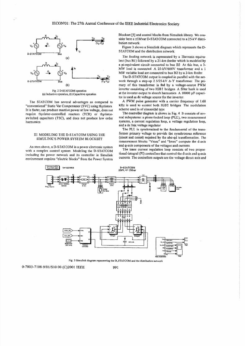
Fig. 1 shows a simplified diagram of a STATCOM con-
nected to a typical distribution network represented by an
equivalent network
B1 82
3MW
0..5 Mvar
Fig . .1 Simpli fied d iagram ofa D-SIJ' l:TCOM connec ted to
a d is tr ib ut io n n et wo rk
The SIATCOM consists mainly of a PWM inverter con-
nected to the network through a transformer Ihe de link volt-
age is provided by capacitor C which is charged with power
taken from the network.The control system ensures the regula-
tion of the bus voltage and the de link voltage.
1 he D-STATCOM function is to regulate the bus voltage by
absorbing or generating reactive power to the network, like a
thyristor static compensator. Ihis reactive power transfer is
done through the leakage reactance of the coupling transformer
by using a secondary voltage in phase with the primary voltage
(network side) .. Ihis Voltage is provided by a voltage-source
PWM inverter The D··STA1COM operation is illustrated by
the phasor diagrams shown in Fig. 2. When the secondary volt-
age (V D) is lower than the bus voltage (VB)' the D-STATCOM
acts like an inductance absorbing reactive power from the bus
When the secondary voltage (V D) is higher than the bus volt-
age (VB)' the D ..STA1COM acts like a capacitor generating
reactive power to the bus. In steady state, due to inverter losses
the bus voltage always leads the inverter voltage by a small
angle to supply a small active power.
990
5/8/2018 Statcom Model Paper - slidepdf.com
http://slidepdf.com/reader/full/statcom-model-paper-559bf4e1099d4 2/5
IECON'Ol: The 27th Annual Conference of the lEEEIndustrial Electronics Society
+~+
Vo t_:_,3VB
D-STATCOM ' Bus
(a)
v : ( ! j v . tD-STATCOM Bus
(b)
F ig . 2 D - SI 'A TCOM o pe ra ti on
(a) Induc ti v e opera ti on, (b) Capaci ti v e opera t ion
The STATCOM bas several advantages as compared to
"conventional" Static Var Compensator (SVC) using thyristors
It is faster; can produce reactive power at low voltage, does not
require thyristor-controlled reactors (TCR) or thyristor-
switched capacitors (TSC), and does not produce low orderharmonics
III MODELING THE D-S TATCOM USING THE
SIMULINK'$ POWER SYSl EM BLOCKSET
As seen above, a D-S rAJCOM is a power electronic system
with a complex control system Modeling the D-STATCOM
including the power network and its controller in Simulink
environment requires "electric blocks" from the Power System
Ts=1/60/3S018
Blockset [5] and control blocks from Simulink library ..We con-
sider-here a ±3MvarD-SJAICOM connected to a2S-kV distri-
bution network.
Figure 3 shows a Simulink diagram which represents the D-
Sl'A:TCOM and the distribution network
I he feeding network is represented by a Thevenin equiva-
lent (bus BI) followed by a 21-km feeder which is modeled by
a pi-equivalent circuit connected to bus B2 At this bus, a 3-
MW load is connected A 25-kV/600V transformer and a 1
MW variable load are connected to bus B2 by a 2-km feeder
The D-STATCOM output is coupled in parallel with the net-
work through a step-up 2 S/2S-kV 6.-Y transformer Th e pri-
mary of this transformer is fed by a voltage-source PWM
inverter consisting oftwo IGBI bridges A filter bank is used
at the inverter output to absorb harmonics A 10000 ~F capaci-
tor is used as de voltage source for the inverter.
A PWM pulse generator with a carrier frequency of 1.68
kHz is used to control both IGBl bridges The modulation
scheme used is of sinusoidal type
The controller diagram is shown in F ig. 4 It consists of sev-
eral subsystems: a phase-locked loop (PLI), two measurementsystems, a current regulation loop, a voltage regulat ion loop,
and a de link voltage regulator
1e PLI is synchronized to the fundamental of the trans-
former primary voltage to provide the synchronous reference
(sinon and cosmt) required by the abc-qd transformation ..The
measurement blocks "Vmes" and "Imes" compute the d-axis
and q-axis components of the voltages and currents
1e inner current regulation loop consists of two propor-
tional-integral (PI) controllers that control the d-axis and q-axis
currents The controllers outputs are the voltage direct ..axis and
D-STATCOM2SkV,...1-3Mvar
0-7803-7108-9/01/$10 00 (C)2001 IEEE
Fig 3 Simul ink d iagram repre sent ing the D_STAICOM and the d is tribu tion network
991
5/8/2018 Statcom Model Paper - slidepdf.com
http://slidepdf.com/reader/full/statcom-model-paper-559bf4e1099d4 3/5
lECON tO 1 ; T he 2 7th Ann ua l C on fe re nc e o f th e IEEE In du stria l E le ctro nic s S oc ie ty
Sign can, . ,oinUCm:
!d pot:lNt{+, ~O'JIj'rng irll~o)~Vll:rtur =10 Convert,,! abSQlt~ real powar-=-P IlO)~lIf+)
Iq negat i V 9{ - ) n :owi n qh, l o-oon ve r l :e r QtId~ CIne!'!!) ""> C o n v e rt e r ; _ b s lJ . r t) i n 9. f a aC ~ 1 f e p:twef = Q po'sHi ve <")
DlaceeteJ-phas.B filL
F ig 4 D -S T Al C OM control system
quadrature-axis components 01d and Vq) that the PWM
inverter has to generate. The Vd and Vq voltages ate converted
into phase voltages Va' Vb' Vcwhich are used to synthesize the
PWM voltages
Ihe network bus voltage is regulated by a PI controller
which produces the Iq reference for current control ler. The Id
reference com es from the dc link vo lt age r egu la to r wh i chmaintains the DC link voltage constant
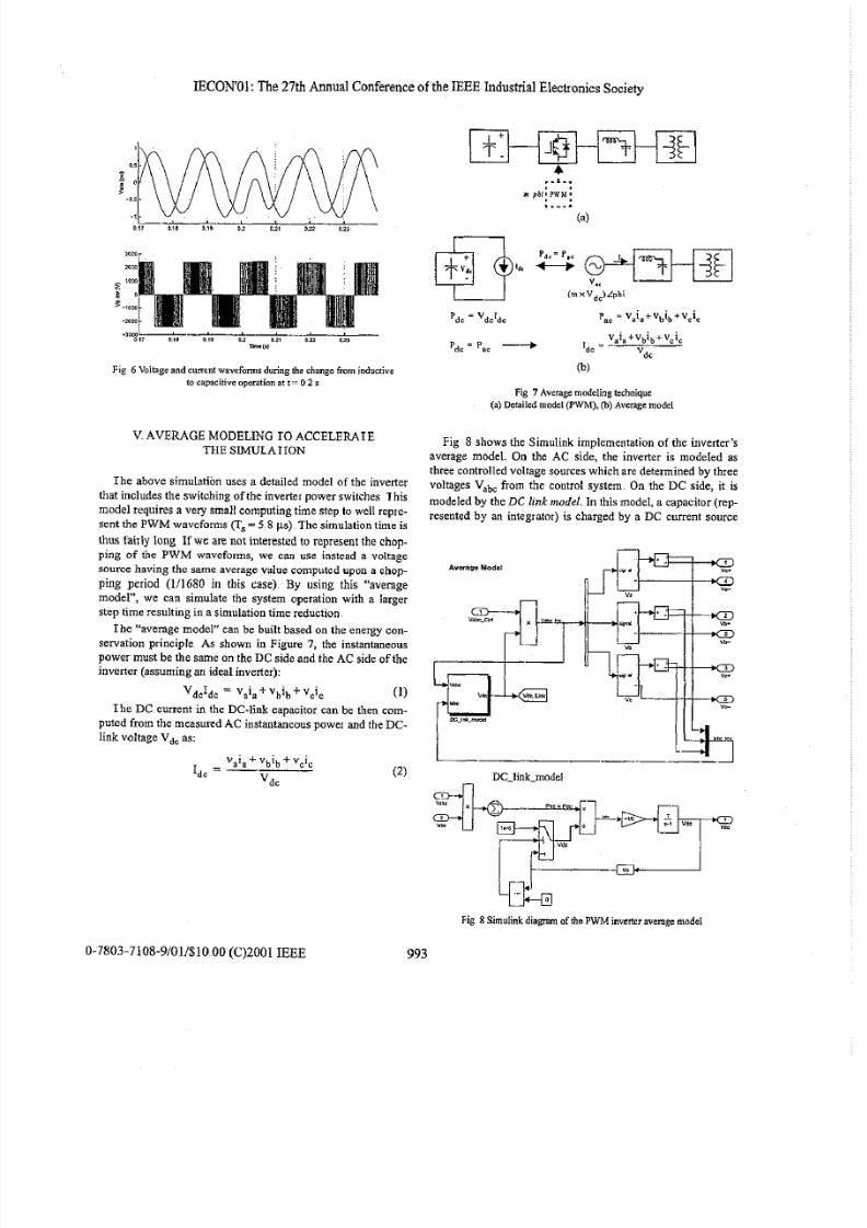
IV SIMULA lING THE D·S IA J COM OPERA nON
The Simulink diagram described above has been used to
simulate the operation of the D·STA:JCOM under different
conditions to illustrate its static and dynamic performance The
simulation was done using a discrete step time (Is = S.8Ils}
Figs. 5 and 6 show the waveforms obtained during a com-
plex test in which the dynamic response of D-STATCOM to
step changes in source voltages is observed
1he PSB Frog Source block is used to modulate the internal
voltage ofthe 2S-kV source>
At starting, the source voltage is such that the D-SIATCOM
is inactive ..Itdoes not absorb nor provide reacfive power to the
network. Att =
0.125 s, the source voltage is increased by 6%The D·S IATCOM compensates for this voltage increase by
absorbing reactive power from the network (Q = +27 Mvar).
At t = 0 2 s, the source voltage is decreased by 6% from the
value corresponding to Q = 0 Then the D-STATCOM must
generate reactive power to maintain a 1pu voltage (Q changes
from +2 >7Mvar to -2..8 MV3I)
0-7803.-7108-9/011$1000 (e)200! IEEE
,~~--;_--------:---'~~= ~ ~ ~ ~ = ~
Tm.(3)
F ig 5 Wavef orms i ll us tr at ing t he D_STAICOM dynamic pe rf ormance
Note that when the D · - S 1A:JCOM changes from inductive to
capacitive operation, the inverter modulation index m is
increased from 0.48 to 087 which corresponds to a propor-
tional increase in inverter voltage . .Reversing of reactive power
flow is very fast (about one cycle) as shown in Fig 6
992
5/8/2018 Statcom Model Paper - slidepdf.com
http://slidepdf.com/reader/full/statcom-model-paper-559bf4e1099d4 4/5
lECON 'O 1 : T he 2 7th A nn ual C on fe ren ce o f th e IEEE In du stria l E le ctro nic s Society
Fig 6 Voltage and current waveforms during the c hange from inductive(0capacitiveoperationat r= 0. 2 s
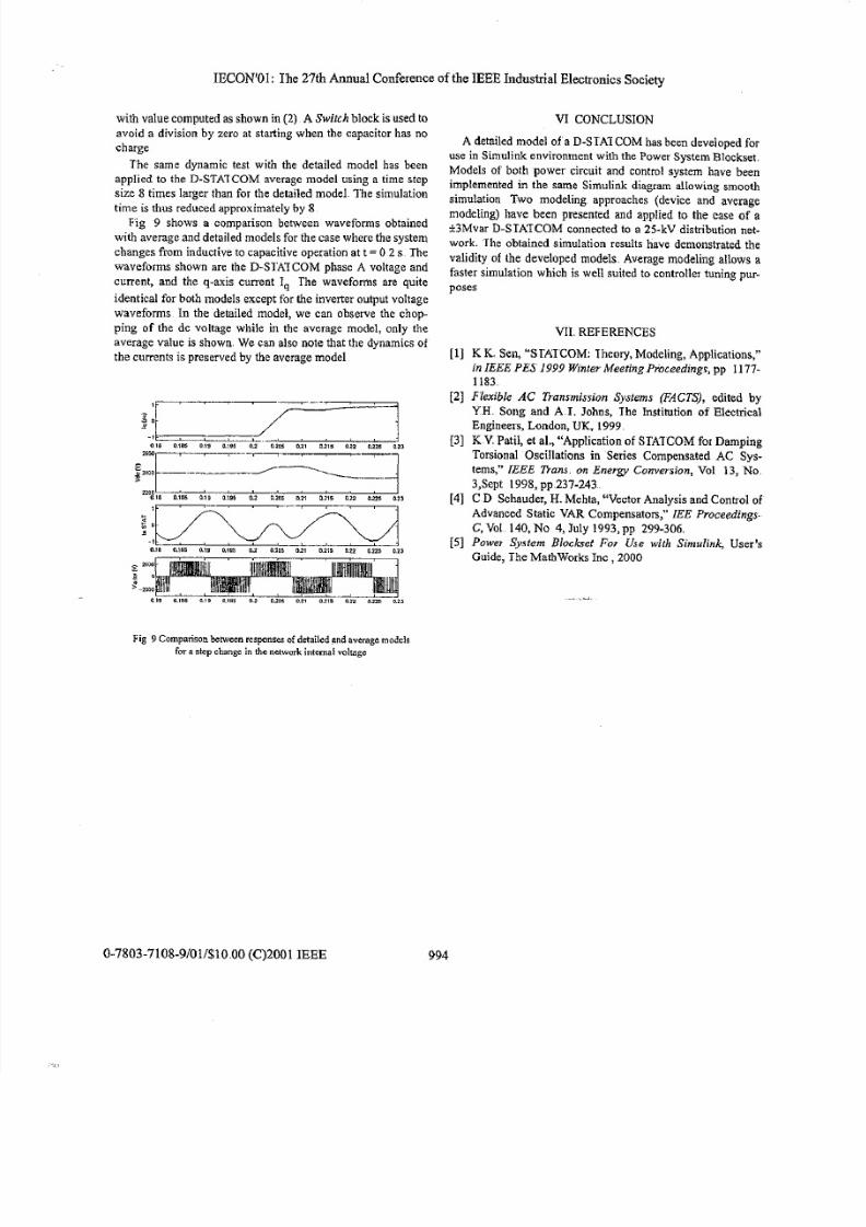
V AVERAGE MODELING roACCELERAIE
THE SIMULATION
Ie above simulation uses a detailed model of the inverter
that includes the switching ofthe inverter power switches 1is
model requires a very small computing time step to well repre-
sent the PWM waveforms (1'5' " 5.8 us) The simulation time is
thus fairly long. If w eare not interested to represent the chop-
ping of the PWM waveforms, we can use instead a voltage
source having the same average value computed upon a chop-
ping period (1/1680 in this case) By using this "average
model", we can simulate the system operation with a larger
step time resulting in a simulation time reduction.
I he "average model" can be built based on the energy con-servation principle. As shown in Figure '7, the instantaneous
power-must be the same on the DC side and the AC side of the
inverter (assuming an ideal inverter):
Vdc1dc ee vaia+vblb+vcic (1)
Ihe DC current in the DC-link capacitor can be then com-
puted from the measured AC instantaneous power and the DC·
link voltage V de as:
0-7803-7108-9/01/$10..00 (C)2001 IEEE
•• .1 _ .
(a)
r ~ f ~ l . g ? d> lt1 1 - 1 H~5 (mXVdc)Lphi
Pac ~ v.i.+vbib+vcic
vaia+Vbib+VcicIdc ~"---v;;--
(b)
F ig 7 A ve ra ge m o de lin g technique(a) Detailed mode l (PWM). (b) Aver ag e mod e l
Fig 8 shows the Simulink implementation of the inverter' s
average model. On the AC side, the inverter is modeled as
three controlled voltage sources which are determined by three
voltages Vabc from the control system. On the DC side, it is
modeled by the DC link model. In this model, a capacitor (rep-
resented by an integrator) is charged by a DC current source
(2)DC_l ink_model
F ig 8 Sim ulin k d ia gram o f t he P WM in ve rter av era ge m od el
993
5/8/2018 Statcom Model Paper - slidepdf.com
http://slidepdf.com/reader/full/statcom-model-paper-559bf4e1099d4 5/5
IECON 'O l: T he 2 7th Ann ua l C on fe re nc e o f th e 1 EEE I nd us tri al E le ctr on ic s S oc ie ty
with value computed as shown in (2). A Switch block is used to
avoid a division by zero at starting when the capacitor has no
charge
The same dynamic test with the detailed model has been
applied to the D-STA1COM average model using a time step
size 8 times larger than for the detailed model. The simulation
time is thus reduced approximately by 8Fig 9 shows a comparison between waveforms obtained
with average and detailed models for the case where the system
changes from inductive to capacitive operation at t=0 2 s. The
waveforms shown are the D-SIA1COM phase A voltage and
current, and the q-axis current Iq The waveforms are quite
identical for both models except for the inverter output voltage
waveforms. In the detailed model, we can observe the chop-
ping of the dc VOltage while in the average model, only the
average value is shown We can also note that the dynamics of
the currents is preserved by the average model.
~ :0.111 0-.1.8.5 o.l!i o.1'J:5 0.2 O,~[I,S 0.21 0.215 D:~2 IL225 0.23-
f~:~I.I~I~>-2000 ~I, I I I '
O.1!11 Q.l85 0.19 0 ;;;:0 0 . . . 2 1).205 0.21 ~.215· 0,2 2 0.:225 :0.23
Fig 9 Comparison between responses of detailed andaverage models
for a step change in the ne twork internal vol tage
0-7803-7108-9/01/$lO.00 (C)2001 IEEE
VI CONCLUSION
A detailed model ofa D-STA1COM has been developed for
use in Simulink environment with the Power System Blockset.
Models of both power circuit and control system have been
implemented in the same Simulink diagram allowing smooth
simulation Two modeling approaches (device and average
modeling) have been presented and applied to the case of a
±3Mvar D-STA:TCOM connected to a 2S-kV distribution net-
work. 'The obtained simulation results have demonstrated the
validity of the developed models. Average modeling allows a
faster simulation which is well suited to controller tuning pur-
poses
VII. REFERENCES
[1] K K Sen, "SIA:ICOM: Theory, Modeling, Applications,"
in IEEE PES 1999 WI'nt e rMee ti ng Proceed ings , pp 1177-
1 1 8 3 .
[2] Flexible AC Transmission Systems (FACTS), edited by
YR, Song and A.L Johns, The Institution of Electrical
Engineers, London, UK, 1999,
[3] K V. Patil, et ai., "Application of SI:A:TCOM for Damping
Torsional Oscillations in Series Compensated AC Sys-
tems," IEEE Trans on Energy Conversion, Vol 13, No.
3,Sept 1998, pp.237-243..
[4] CD Schauder, H.Mehta, "Vector Analysis and Control of
Advanced Static VAR Compensators," lEE Proceedings-
C, VoL 140, No 4, July 1993, pp 299-306.
[5] Power System Blockset For Use with Simulink, User's
Guide, The MathWorks Inc, 2000
994