static power reduction techniques for asynchronous...
TRANSCRIPT

STATIC POWER REDUCTION TECHNIQUES FORASYNCHRONOUS CIRCUITS
A Thesis
Presented to the Faculty of the Graduate School
of Cornell University
in Partial Fulfillment of the Requirements for the Degree of
Master of Science
by
Carlos Tadeo Ortega Otero
May 2012

© 2010 Cornell University
ALL RIGHTS RESERVED

ABSTRACT
Power gating techniques are effective in mitigating leakage losses, which rep-
resent a significant portion of power consumption in nanoscale circuits. We ex-
amine variants of two representative techniques, Cut-Off and Zig-Zag Cut-Off
[12], and find that they offer an average of 80% and 20% in power savings, re-
spectively, for asynchronous circuit families. We also present a new zero-delay
(ZDRTO) wakeup technique for power gated asynchronous pipelines, which
leverages the robustness of asynchronous circuits to delays and supply voltage
variations. Our ZDRTO technique offers a trade off between wake up time and
static power reduction, making it suitable for power gating pipelines with low-
duty cycle, bursty usage patterns.

BIOGRAPHICAL SKETCH
Carlos Tadeo Ortega Otero was born in Mexico City, Mexico where he grew up.
Carlos received the B.S. degree in Computer Engineering from the Instituto Tec-
nologico de Monterrey, campus Estado de Mexico, in 2006. He is currently pur-
suing the Ph.D. degree in Electrical Engineering at Cornell University in Ithaca,
NY. His current research interests include low-power Very Large Scale Integra-
tion (VLSI), computer-aided design tools for VLSI automation, asynchronous
integrated circuit design, emerging VLSI technologies, and secure VLSI systems.
Carlos is part of the Asynchronous VLSI Group and Architecture (AVLSI)
led by Professor Rajit Manohar.
iii

To: Bistra, mama & papa
iv

ACKNOWLEDGEMENTS
This research project was only possible with the kind support from many
people. Undoubtedly, the most influential person in my career is Prof Rajit
Manohar. Rajit’s passion for VLSI and Asynchronous circuits has encouraged
me to learn in depth different concepts and link them together to build new
ideas. His unsurpassed knowledge of various areas of VLSI and Computer Sci-
ence has been extremely resourceful throughout my tenure at Cornell. I would
also like to thank all professors at the Computer Systems Lab for their thought-
ful comments while I was preparing this work.
David Fang and Filipp Akopyan were my first mentors at Cornell. They
were the first who taught me Asynchronous Circuits, VLSI, and how to use the
different tools available in the lab. Filipp has always encouraged me to work
harder each day to achieve my goals. Ilya Ganusov and Basit Riaz always made
research seem fun and fascinating. I would like to acknowledge Nabil for his
contribution on static power reduction for SRAMS. I would like to thank the λ-
team: Robert Karmazin, Benjamin Hill and Jonathan Tse. I would especially like
to thank Jonathan Tse for being my closest collaborator and friend throughout
my graduate studies — his contribution on the control system and the uncount-
able discussions with him were vital to finish this project.
My family has been a veritable network of support through difficult times
during my research. My wife Bistra Dilkina has always been next to me, and
every day creates a better version of me. My parents Myrna and Rodolfo and
my siblings have encouraged me whenever the morale was low. I would also
like to thank Edgar, Isauro, Lourdes and Mauricio.
Finally, I would like to thank the funding agencies for their generous contri-
bution to this project: Blue Highway and CONACyT, as well as Intel Corpora-
tion for the donation of equipment to the Computer Systems Lab.
v

TABLE OF CONTENTS
Biographical Sketch . . . . . . . . . . . . . . . . . . . . . . . . . . . . . . iiiDedication . . . . . . . . . . . . . . . . . . . . . . . . . . . . . . . . . . . ivAcknowledgements . . . . . . . . . . . . . . . . . . . . . . . . . . . . . . vTable of Contents . . . . . . . . . . . . . . . . . . . . . . . . . . . . . . . viList of Tables . . . . . . . . . . . . . . . . . . . . . . . . . . . . . . . . . . viiiList of Figures . . . . . . . . . . . . . . . . . . . . . . . . . . . . . . . . . ixList of Abbreviations . . . . . . . . . . . . . . . . . . . . . . . . . . . . . 1
1 Introduction 2
2 Transistor Leakage Mechanisms 52.1 Subthreshold leakage current (IOFF) . . . . . . . . . . . . . . . . . . 6
2.1.1 Reverse biased diode current (IINV) . . . . . . . . . . . . . . 72.1.2 Subthreshold drain current (ID,WEAK) . . . . . . . . . . . . . 82.1.3 Gate-induced drain current (IGIDL) . . . . . . . . . . . . . . 92.1.4 Analysis of Subthreshold leakage currents . . . . . . . . . 9
2.2 Gate Leakage (IGAT E) . . . . . . . . . . . . . . . . . . . . . . . . . . 132.2.1 Gate tunneling (ITUNNEL) . . . . . . . . . . . . . . . . . . . . 142.2.2 Hot Carrier injection (IHC) . . . . . . . . . . . . . . . . . . . 14
2.3 The impact of CMOS device scaling in leakage currents . . . . . . 142.3.1 Gate Oxide Thickness (Tox) scaling . . . . . . . . . . . . . . 152.3.2 Channel miniaturization . . . . . . . . . . . . . . . . . . . . 162.3.3 Vdd and Vth scaling . . . . . . . . . . . . . . . . . . . . . . . 162.3.4 Doping concentration . . . . . . . . . . . . . . . . . . . . . 172.3.5 Source-Drain punchthrough . . . . . . . . . . . . . . . . . . 17
3 Static power reduction techniques 183.1 Device Engineering . . . . . . . . . . . . . . . . . . . . . . . . . . . 183.2 Circuit Engineering . . . . . . . . . . . . . . . . . . . . . . . . . . . 193.3 System Engineering . . . . . . . . . . . . . . . . . . . . . . . . . . . 20
4 Power Gating techniques 224.1 Non-State Preserving Power Gating . . . . . . . . . . . . . . . . . 234.2 State Preserving Power Gating . . . . . . . . . . . . . . . . . . . . 25
5 Asynchronous Power Gating 285.1 Pseudo-Static Logic Overview . . . . . . . . . . . . . . . . . . . . . 285.2 Non-State Preserving . . . . . . . . . . . . . . . . . . . . . . . . . . 295.3 State Preserving . . . . . . . . . . . . . . . . . . . . . . . . . . . . . 33
6 Zero-delay ripple turn on (ZZDRTO) 356.1 Zero-Delay Ripple Turn On . . . . . . . . . . . . . . . . . . . . . . 356.2 Empty Pipeline Detection . . . . . . . . . . . . . . . . . . . . . . . 38
vi

7 Evaluation 417.1 Methodology . . . . . . . . . . . . . . . . . . . . . . . . . . . . . . 417.2 Power Gating Evaluation . . . . . . . . . . . . . . . . . . . . . . . . 427.3 ZDRTO Evaluation . . . . . . . . . . . . . . . . . . . . . . . . . . . 46
8 Discussion 53
9 Conclusion 54
Bibliography 55
vii
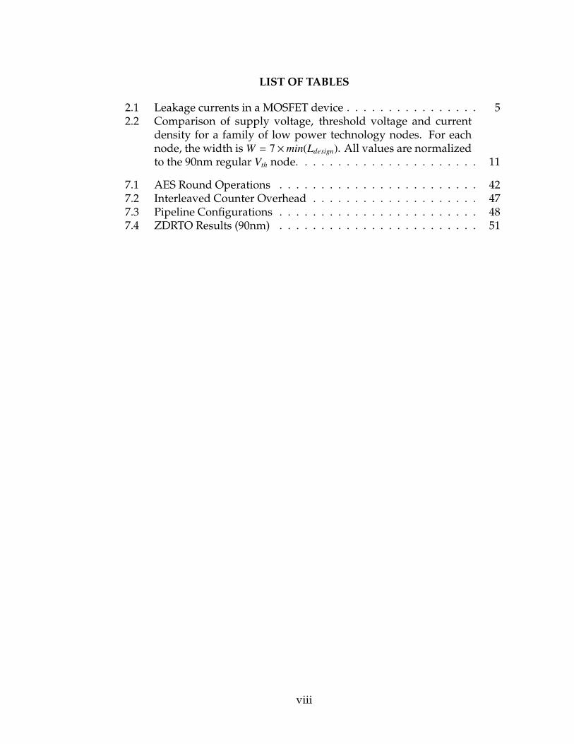
LIST OF TABLES
2.1 Leakage currents in a MOSFET device . . . . . . . . . . . . . . . . 52.2 Comparison of supply voltage, threshold voltage and current
density for a family of low power technology nodes. For eachnode, the width is W = 7×min(Ldesign). All values are normalizedto the 90nm regular Vth node. . . . . . . . . . . . . . . . . . . . . . 11
7.1 AES Round Operations . . . . . . . . . . . . . . . . . . . . . . . . 427.2 Interleaved Counter Overhead . . . . . . . . . . . . . . . . . . . . 477.3 Pipeline Configurations . . . . . . . . . . . . . . . . . . . . . . . . 487.4 ZDRTO Results (90nm) . . . . . . . . . . . . . . . . . . . . . . . . 51
viii

LIST OF FIGURES
2.1 Traversal view of a MOSFET device showing all Leakage currents 62.2 Traversal view of a transistor showing subthreshold leakage cur-
rents . . . . . . . . . . . . . . . . . . . . . . . . . . . . . . . . . . . 72.3 Experimental setup to measure the subthreshold leakage current
IOFF . The drain current of an n-fet sized W = 7 × min(Ldesign) ismeasured across different values of Vg and Vd. . . . . . . . . . . . 11
2.4 Subthreshold slope for a family of 90nm, 65nm and 32nm lowpower technologies. The 90nm Rvt at Vd = 0.2 transfer curve isplotted across all technologies as a reference point. . . . . . . . . 12
2.5 Gate leakage current Ig as a function of Vgs for multiple technol-ogy nodes . . . . . . . . . . . . . . . . . . . . . . . . . . . . . . . . 13
3.1 [A]Natural stacks found in a NAND gate. [B]Forced stacking onthe pull-down network of an inverter . . . . . . . . . . . . . . . . 20
4.1 Cut-Off (CO) power gating using a foot sleep transistor, which isshared by several logic blocks. The output nodes tend to drift togvssv, which itself drifts towards VDD. . . . . . . . . . . . . . . . . 22
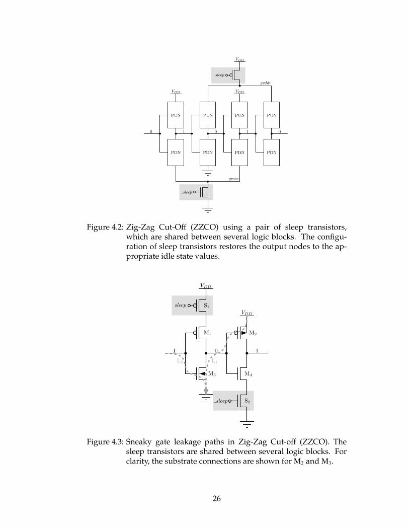
4.2 Zig-Zag Cut-Off (ZZCO) using a pair of sleep transistors, whichare shared between several logic blocks. The configuration ofsleep transistors restores the output nodes to the appropriate idlestate values. . . . . . . . . . . . . . . . . . . . . . . . . . . . . . . . 26
4.3 Sneaky gate leakage paths in Zig-Zag Cut-off (ZZCO). The sleeptransistors are shared between several logic blocks. For clarity,the substrate connections are shown for M2 and M3. . . . . . . . . 26
5.1 (a) Pseudo-Static CMOS Gate, (b) Weak Feedback Inverter . . . . 295.2 Self reset circuit behavior immediately after sleep goes low. . . . . 325.3 Zig-Zag Power Gating with Weakened Staticizers (ZZCO-WS)
using (a) Virtual Power Rails or (b) Sleep Signals . . . . . . . . . 34
6.1 Block diagram of our Zero-Delay Ripple Turn On (ZDRTO)power gating control scheme. A sample pipeline of 8-stages isdivided into three unequal clusters: C0, C1, and C2. Each clustercontrols the power gating of the next inline cluster. With respectto Eq. 6.1, j = i + 1. . . . . . . . . . . . . . . . . . . . . . . . . . . . 36
7.1 Static power consumption of each AES round operation. Eachoperation is power gated in isolation, and results are normalizedto a baseline implementation of no power gating. . . . . . . . . . 43
7.2 Average operating frequency of each AES round operation. Eachoperation is power gated in isolation, and results are normalizedto a baseline implementation of no power gating. . . . . . . . . . 44
ix

7.3 Transient behavior of CO power gating. Note the peak in supplycurrent immediately after sleep is asserted at t = 100ns. . . . . . . 45
7.4 Evaluation of ZZDRTO technique using different clusteringschemes . . . . . . . . . . . . . . . . . . . . . . . . . . . . . . . . . 49
7.5 Trade off curve of wake up time vs leakage for multiple experi-ments . . . . . . . . . . . . . . . . . . . . . . . . . . . . . . . . . . 52
x
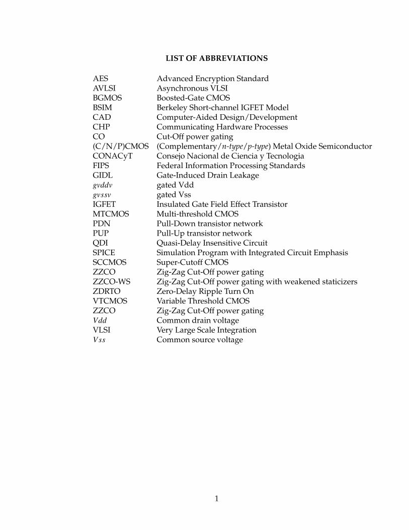
LIST OF ABBREVIATIONS
AES Advanced Encryption StandardAVLSI Asynchronous VLSIBGMOS Boosted-Gate CMOSBSIM Berkeley Short-channel IGFET ModelCAD Computer-Aided Design/DevelopmentCHP Communicating Hardware ProcessesCO Cut-Off power gating(C/N/P)CMOS (Complementary/n-type/p-type) Metal Oxide SemiconductorCONACyT Consejo Nacional de Ciencia y TecnologiaFIPS Federal Information Processing StandardsGIDL Gate-Induced Drain Leakagegvddv gated Vddgvssv gated VssIGFET Insulated Gate Field Effect TransistorMTCMOS Multi-threshold CMOSPDN Pull-Down transistor networkPUP Pull-Up transistor networkQDI Quasi-Delay Insensitive CircuitSPICE Simulation Program with Integrated Circuit EmphasisSCCMOS Super-Cutoff CMOSZZCO Zig-Zag Cut-Off power gatingZZCO-WS Zig-Zag Cut-Off power gating with weakened staticizersZDRTO Zero-Delay Ripple Turn OnVTCMOS Variable Threshold CMOSZZCO Zig-Zag Cut-Off power gatingVdd Common drain voltageVLSI Very Large Scale IntegrationV ss Common source voltage
1

CHAPTER 1
INTRODUCTION
Reducing power consumption has become very important in recent years due to
increases in transistor density and clock frequency as well as consumer trends
in high-performance, portable, and embedded applications. Dynamic power
losses are significant, but can be mitigated by techniques such as clock gating,
which reduces the power consumption of idle sections of synchronous circuits
[34]. Asynchronous designs offer this advantage inherently, as they are data
driven and are only active while performing useful work. In other words, asyn-
chronous circuits implement the equivalent of a fine-grained clock gating net-
work. However, while dynamic power loss has been dominant culprit in the
past, static power loss has become a considerable contributor to power con-
sumption in nanoscale technologies [16, 29] due to leakage currents.
One of the main causes of static power loss are leakage currents. There are
a wide array of techniques designed to reduce leakage currents [31, 10, 32].
The most effective techniques involve power gating circuits — essentially cut-
ting off the pull-up network (PUN) and pull-down network (PDN) from one
or both power rails during idle or “sleep” periods. During active periods, the
circuit is reconnected to the power rails in a process known as “wake up” or
power up. While power gating has been adapted for use in asynchronous cir-
cuits [12, 35, 20], most of these efforts involve direct application of synchronous
techniques to asynchronous systems. As such, the unique capabilities of asyn-
chronous circuits have not been fully leveraged in the context of power gating.
Many asynchronous circuit families are robust to a wide range of supply
voltages, ambient temperatures, and process variations [1]. We exploit this ro-
2

bustness in the context of power gating to enable a zero-delay wake up scheme for
pipelined computation: the first token traveling through a pipeline turns on down-
stream pipeline stages, hiding the latency cost of wake up in the computation
time of upstream pipeline stages.
Synchronous circuits cannot take full advantage of such aggressive power
gating control schemes, as local supply voltages must reach nominal values
to prevent the synchronous circuit from violating its timing requirements, e.g.
setup/hold constraints on state-holding elements. Therefore, inputs can only be
applied to a pipeline stage once the supply voltage has reached an acceptable
threshold. By leveraging the supply voltage operating range of asynchronous
circuits, we can avoid this requirement and begin useful computation before
the supply voltage has stabilized, reducing the forward latency seen by the first
input token.
Chapter 2 examines the leakage mechanisms of CMOS transistors. A thor-
ough understanding of such mechanisms is crucial to develop techniques to
mitigate static power consumption in Asynchronous Circuits. We analyzed dif-
ferent technology nodes and the impact of technology scaling in leakage current.
Chapter 3 briefly explores the most common techniques that are used to re-
duce static power consumption at different stages of the design process of full
custom integrated circuits.
Chapter 4 presents a general overview of the two main classes of power gat-
ing techniques: (i) Non-state preserving, and (ii) State-preserving. Asynchronous
circuits contain many pseudo-static gates, and robust circuit families like quasi-
delay insensitive (QDI) asynchronous logic contain a significantly higher num-
3

ber of pseudo-static gates than an equivalent synchronous computation. To this
end, we discuss the implementation details of power gating asynchronous cir-
cuits in Chapter 5, which focuses on applying non-state preserving and state
preserving techniques to pseudo-static elements. Our evaluation of these tech-
niques is given in Chapter 7.2. In Chapter 6, we formalize the aforementioned
zero-delay wake up power gating control methodology, which we call Zero-
Delay Ripple Turn On (ZDRTO), and discuss our method of empty pipeline de-
tection, a key component in power gating. Finally, in Chapter 7.3, we present
the results of our evaluation of ZDRTO, as well as a discussion of appropriate
use cases.
The work presented in this thesis, and the ZZDRTO technique were done
in collaboration with Jonathan Tse. Jonathan is a Ph.D. candidate at the Asyn-
chronous VLSI group and Architecture group at Cornell University. Jonathan
interests include high-speed links, low power design, and security. The inter-
leaved counter for the empty pipeline detection and the self-reset circuitry are
entirely his work, both of them are included in this text for completeness.
4

CHAPTER 2
TRANSISTOR LEAKAGE MECHANISMS
The exponential increase of the number of on chip active devices, the con-
stant decrease of the threshold Voltage (Vth) and reduction of the gate oxide
thickness (Tox) result in a significant amount of static power in circuits designed
in deep sub-micron technologies. Static power consumption is generated by
leakage currents, that is the currents that flow through the devices when the
total current should be 0A. Increase in leakage power is the a big concern that
circuit designers need to address, particularly for circuits that have low-duty
cycles, bursty operation and rely on batteries for long periods of time. There are
many scenarios that generate leakage currents, and understanding such condi-
tions is crucial to understanding how to abate them. This chapter summarizes
the main transistor leakage mechanisms for short-channel CMOS devices. Al-
though most of the discussion in this chapter is rendered for an n-type MOS
transistor, an analogous analysis can be produced for a p-type MOS transistor.
Table 2.1: Leakage currents in a MOSFET device
IOFF
Subthreshold drain current(ID,WEAK)
Reverse biased current (IINV)
Gate Induced drain leakage (IGIDL)
IGAT E
Gate tunneling (ITUNNEL)
Hot Carrier Injection (IHC)
Rather than a single component, the total leakage current is the addition of
several parasitic currents. These currents can be classified in two main cate-
gories: i) drain leakage current that flows from the drain to the source or the
5

Gate(G) Drain(D)Source(S)
Substrate
Iinv
ITUNNEL
IGIDL
ID,weak
IHC
Figure 2.1: Traversal view of a MOSFET device showing all Leakage cur-rents
body (IOFF); and ii) leakage current that dribbles through the gates of the tran-
sistor (IGAT E).
IGAT E and IOFF are the compound of currents generated by multiple physical
effects under specific circumstances. Table 2.1 summarizes the main compo-
nents that contribute for IGAT E and IOFF . Figure 2 shows the leakage currents in
a traversal cut of an n-type transistor. The rest of this chapter briefly describes
the conditions that allows static power consumption in digital circuits.
2.1 Subthreshold leakage current (IOFF)
The subthreshold leakage current of a transistor, IOFF , is defined as the drain
current when |Vg| − |Vs| = 0 and Vd ≥ 0. IOFF is dependent on the circuit topology
and device physics such as Vdd, Vth, doping concentration, and gate oxide thick-
ness Tox. IOFF is composed of several sub-components as shown in Fig. 2.1, and
can be expressed as the sum of these components as shown in Eq. 2.1.
6

Gate(G) Drain(D)Source(S)
Substrate
Iinv
ID,weak
IGIDL
Figure 2.2: Traversal view of a transistor showing subthreshold leakagecurrents
IOFF = IINV + ID,WEAK + IGIDL (2.1)
2.1.1 Reverse biased diode current (IINV)
IINV is the current that flows through the reverse biased diode between the drain
(n-region) and the p-region of the transistor, and it is dependent on the junction
area between the Source/Drain terminals and the body and exponentially de-
pendent to the temperature [23, 3].
The leakage current for the inverse biased diode is given by Eq. 2.2, where
UT is the thermal Voltage, a parameter linearly dependent on the voltage. Is
is an intrinsic parameter for the device, usually known as the reverse saturation
current and Vd is the voltage between the drain and the body of the transistor.
Because of the exponential dependence on the voltage, any small perturbation
will set the value of the reverse biased diode current (IINV) near the value of the
saturation current (Is). Sometimes, electric data-sheets only provide the satura-
7

tion current density Jinv, in which case one can compute the reverse biased diode
current by multiplying the current density by the diffusion area Ad as described
by equation 2.3.
IINV = Is
(e(Vd/Ut) − 1
)(2.2)
IINV = Ad × Jinv (2.3)
2.1.2 Subthreshold drain current (ID,WEAK)
Consider a transistor with Vg < Vth, |Vd| ≥ 0.1 and Vs = Vb = 0. Under these
conditions, the transistor is said to be in weak inversion. A transistor in weak
inversion has a constant voltage across the channel and the magnitude of the
longitudinal component of the electric field across the channel is 0. Hence, there
is no drift current. Instead, the leakage current ID,WEAK is produced by the dif-
fusion of majority carriers across the channel [36]. ID,WEAK can be modeled as
described in Eq. 2.4, where Ut is the thermal voltage and I0 is an initial DC off-
set in the drain current. It is important to note the exponential dependency of
ID,WEAK on Vgs as well as a linear offset based on VDS .
Id,weak =WL× I0 × e(Vgs−Vth)(mUT )−1
×(1 − e−VDS (mU−1
T ))
(2.4)
8
2.1.3 Gate-induced drain current (IGIDL)
Gate-induced drain leakage, IGIDL, is generated when a large-enough gate-to-
drain (Vgd) voltage is applied to produce a band-to-band electron tunneling near
the interface between the gate oxide and the semiconductor of the drain.
2.1.4 Analysis of Subthreshold leakage currents
The effectiveness of how much a transistor controls the drain current IOFF when
Vg ≤ Vth is measured by the subthreshold slope, which is the resulting line of a
semi-logarithmic scale plot of the Vgs - Id transfer curve. Since ID,WEAK depends
also on Vds, one can draw different subthreshold slopes for multiple values of
Vds.
We analyzed and compared subthreshold slopes for commercially available
90nm, 65nm and 32nm low-power technology nodes. The results are presented
in Fig. 2.4. The experiment was setup using the schematic as shown in Fig. 2.1.4.
Vgs was swept from 0 to Vth and the log(Id) was plotted for Vd = 0.2V , Vd = 0.5V ,
Vd = 0.8V , and Vd = 1.2V , the foundry provides regular-Vt (Rvt) and high-Vt(Hvt),
the subthreshold slope for both device types are presented too. The range of the x-
and y- axis is the same across all plots, however the axis labels were removed in
compliance with our agreement with the foundry. The subthreshold slope for
90nm Rvt, Vdd = 0.2 is presented across all other plots as a reference point.
Although a direct comparison between the plots in Fig. 2.1.4 is not meaning-
ful, we can draw some qualitative conclusions from these plots: High-Vth (Hvt)
processes have lower subthreshold leakage than their regular-Vt (Rvt) counter-
9

parts, which is expected from Eq. 2.4. These plots also allow to visually quantify
the high leakage reduction gains that the use of Hvt transistors yields. Fig. 2.4
also shows that the slope is slightly steeper for the Rvt transistors, which was
probably engineered to allow a faster transition between the weak inversion
and strong inversion state as Vgs reaches Vth.
The use of Hvt for sleep transistors plays a very important role in maximiz-
ing the leakage power savings using power-gating techniques. If idle power
consumption needs to be optimized for an application, the designer should ex-
amine the subthreshold slopes to choose the technology node that fits best.
One of the best ways to compare subthreshold currents for different tech-
nology nodes is to compare the leakage per one micron meter of width (W) as
shown in E. 2.5. During this comparison, the length (L) and other conditions re-
main constant. Table 2.2 shows such a comparison of the subthreshold leakage
when Vg = 0. We normalized all values with respect to the 90nm Rvt node. From
the stand point of subthreshold leakage, the 90nm Hvt node performs the best,
while the 32nm Rvt node performs the worst, presumably because of intensified
short-channel effects. Overall, the 65nm node is a good compromise since its
Hvt version leakage currents is almost as good the 90nm Hvt counterpart and the
65nm Rvt node outperforms all other Rvt transistors.
The slight increase in the leakage current density (Jo f f ) shown in Table 2.2
as device length scales down is not as dramatic as previously suggested. We
attribute this to a more aggressive reduction of Vdd and a more conservative
reduction of Vth. It is unknown to the authors the material used as dielectric for
the gate of the transistors.
10

Jo f f =Io f f
W(2.5)
Table 2.2: Comparison of supply voltage, threshold voltage and currentdensity for a family of low power technology nodes. For eachnode, the width is W = 7×min(Ldesign). All values are normalizedto the 90nm regular Vth node.
Node Vdd/Vdd0 Vth/Vth0Jo f f
Jd0when Vd = 0.2V,Vg = 0
90nm Rvt 1 1 1
65nm Rvt 1 0.95 0.210
32nm Rvt 0.8 0.95 2.40
90nm Hvt 1 1.25 0.073
65nm Hvt 1 1.25 0.120
32nm Hvt 0.8 1.12 0.608
Vg
Ioff
Vd
W=7*Lmin
Figure 2.3: Experimental setup to measure the subthreshold leakage cur-rent IOFF . The drain current of an n-fet sized W = 7×min(Ldesign)is measured across different values of Vg and Vd.
11

Vgs
(V)
log(
I d)
Subthreshold Slope n−fet 90nm Rvt
, W=7×Lmin
Id0, V
d=0.2 (Reference)
Vd=0.5
Vd=0.8
Vd=1.2
Vgs
(V)
log(
I d)
Subthreshold Slope n−fet 90nm Hvt
, W=7×Lmin
Id0 (Reference)
Vd=0.2
Vd=0.5
Vd=0.8
Vd=1.2
Vgs
(V)
log(
I d)
Subthreshold Slope 65nm Rvt
, W=7×Lmin
Id0 (Reference)
Vd=0.2
Vd=0.5
Vd=0.8
Vd=1.2
Vgs
(V)
log(
I d)
Subthreshold Slope n−fet 65nm Hvt
, W=7×Lmin
Id0 (Reference)
Vd=0.2
Vd=0.5
Vd=0.8
Vd=1.2
Vgs
(V)
log(
I d)
Subthreshold Slope n−fet 32nm Rvt
, W=7×Lmin
Id0 (Reference)
Vd=0.2
Vd=0.5
Vd=0.8
Vgs
(V)
log(
I d)
Subthreshold Slope n−fet 32nm Hvt
, W=7×Lmin
Id0 (Reference)
Vd=0.2
Vd=0.5
Vd=0.8
Figure 2.4: Subthreshold slope for a family of 90nm, 65nm and 32nm lowpower technologies. The 90nm Rvt at Vd = 0.2 transfer curve isplotted across all technologies as a reference point.
12

Vgs
(V)
I g
Gate Leakage for a family of low−power families
90nm R
vt
90nm Hvt
65nm Rvt
65nm Hvt
32nm Rvt
32nm Hvt
Figure 2.5: Gate leakage current Ig as a function of Vgs for multiple tech-nology nodes
2.2 Gate Leakage (IGAT E)
The gate leakage manifests itself as current that dribbles across the gate to and
from the channel, substrate, and diffusion terminals. This current disallows
the treatment of the gate of a device as an ideally insulated electrode. The gate
leakage is compounded by two main elements[30]: Gate tunneling (ITUNNEL) and
Hot Carrier injection (IHC).
13

2.2.1 Gate tunneling (ITUNNEL)
This current is created due to carriers tunneling through the gate of the transis-
tor. There are two ways carriers can tunnel through the gate: i) into the con-
duction band of the dielectric (commonly Silica: S iO2), this is known as Fowler-
Nordheim tunneling and it manifests itself as an electron emission caused by
the intense high electric field; and ii) directly to/from the gate through the for-
bidden band gap of the dielectric [27, 9].
2.2.2 Hot Carrier injection (IHC)
This current is known as hot carrier leakage, this current is generated whenever
a carrier gains sufficient kinetic energy to overcome the gate potential barrier.
This effect is more likely for the electron since the voltage barrier and effective
mass of an electron is less than the one for holes.
2.3 The impact of CMOS device scaling in leakage currents
For the past 40 years, circuit designers have had the luxury of inexpensively
doubling the number of transistors every two years, which is possible thanks to
the miniaturization of devices and the reduction of the cost of computer power
due to sales volume. While this trend is slowing down, it will continue (at least)
for the near future. The main problem rises as transistor miniaturization reaches
atomic levels: photolithography, manufacturing costs, increased power density
and the ION/ILEAKAGE current ratio are just some of the challenges that scientists
14

face. While the trend of some leakage currents are to shrink (IINV), some others
significantly increased (ITUNNEL, ID,WEAK), this section explores the trends of de-
vice miniaturization and their impact on the leakage currents described above.
2.3.1 Gate Oxide Thickness (Tox) scaling
Gate oxide thickness in S iO2 CMOS devices is one of the most important param-
eters on a FET device. Traditionally the Tox has scaled such that Le f f = 45 × Tox.
This relationship usually leads to good VG − Id transfer behavior [26]. As the
channel scales under the 100µm this scale is not feasible, since the Tox reaches its
minimum limit. Previous work has set the barrier limit from 12Å to 16Å, which
is the limit where dynamic gate leakage power equals 1A/cm2 for large MOS
capacitors [28].
There are two leakage currents directly affected by reducing Tox: GIDL (Sec.
2.1) and Gate Direct Tunneling. GIDL currents increase, since the voltage re-
quired to generate electron tunneling decreases as gate oxide thickness shrinks.
Although GIDL could impose a limit on scaling the Tox, its effect is expected to
be less relevant for digital applications as the voltage reduces below the energy
band gap of the silicon. Direct tunneling and hot carrier injection is expected to
increase significantly as the thin oxide layers become smaller than 20Å. Despite
the industry hesitation to discontinue Silica as the insulator of gate terminal,
the use of other dielectrics will allow more aggressive reduction of the oxide
thickness in the near future.
15
2.3.2 Channel miniaturization
Short-channel effects are expected to worsen when channel length is reduced.
Drain Induced Barrier Lowering (DIBL) is one of such effects, in which the de-
pletion region of the source/drain extends into the channel of a MOSFET device,
effectively reducing the channel length. This reduction on the depletion region
lowers the potential barrier for electrons, which results in an observable lower-
ing of Vth, and hence in an increase on the ID,WEAK current as seen in E. 2.4. On
the other hand, channel miniaturization reduces the junction area between the
substrate and the Source/Drain, effectively reducing the (IINV)
Channel miniaturization is also closely related to scaling of the Tox, since
both channel and gates are engineered for optimum performance and low
power consumption.
2.3.3 Vdd and Vth scaling
Two of the most important transistor characteristics are the nominal Vdd and Vth.
Process engineers typically scale the supply voltage (Vdd) to control dynamic
power consumption and power density. This reduction in Vdd forces a reduction
in Vth in order to get performance gains. This reduction in Vth typically causes a
relatively large increase in IOFF , while the reduction of Vdd reduces the leakage
currents substantially. The effects of GIDL in technologies that have a nominal
Vdd ≤ 1.1 (energy band gap of Silicon) decay drastically, becoming less of a
concern in digital circuits [4].
16

2.3.4 Doping concentration
The electric field at a p-n junction strongly depends on the junction doping [30].
When device engineers scale-down transistors, the doping concentration is gen-
erally increased, incrementing the overall Iinv and ITUNNEL. However, device sci-
entists engineer smart doping profiles for the channel and the transistor termi-
nals to maximize active current drive while minimizing idle-current.
2.3.5 Source-Drain punchthrough
In an overly simplistic way, punchthrough happens when the depletion regions
from the source and the drain join in the absence of a depletion region induced
by gate [36]. Punchtrough happens when voltages between the source and the
body are above the nominal range of Vdd, since this is not the common case for
digital circuits, this is usually not a concern for ASIC designers. We ran SPICE
simulations, but we did not find any source-drain punchthrough. It is unclear
to the authors if the SPICE deck provides information to model punchthrough.
If punchthrough is a concern, one can model it accurately using a 2-D physical
simulator.
17

CHAPTER 3
STATIC POWER REDUCTION TECHNIQUES
Static power reduction techniques can be classified in three main categories
depending on the granularity at which can be applied:
1. Device Engineering. It refers to techniques that are implemented on the
underlying transistors that conform circuits.
2. Circuit Engineering. It refers to techniques that are applied to gates, which
are clusters of transistors that perform a small computation like NAND,
NOR.
3. System Engineering. It refers to techniques that can are applied to macro-
blocks that are part of a big datapath or micro-chip.
This chapter briefly describes the most common techniques on each of the
categories and discusses the advantages and disadvantages of each one of them.
3.1 Device Engineering
Researchers have developed engineering techniques to reduce leakage on
CMOS devices. Unfortunately, these techniques usually have trade-offs in
performance and area. In order to control static power, device engineers
can modify certain dimensions of the device (e.g., Le f f , Tox, substrate depth,
S ource/Drianoverlap), the nominal values of Vdd and Vth, the materials used (choice
of gate dielectric, semiconductor), the FET-type (depleted devices, bulk devices,
multiple gate devices), the doping profile and doping halo[30].
18

The advantages of tuning transistors are vast since leakage reduction is usu-
ally significant and devices are agnostic to circuit paradigms and logic families.
The main disadvantage of device engineering is that oftentimes the circuit de-
signer has no control over the selection of devices and most likely lacks the
expertise, time, and budget to modify the underlying transistors that conform
circuits. However, it is not uncommon for a design team to be presented with a
portfolio of technologies and manufacturing processes, it is their responsibility
to choose the one that fits the needs of the application. If the main concern is
leakage power consumption, an educated decision when choosing a technology
can be done by analyzing parameters like the ones discussed in Chapter 2.
3.2 Circuit Engineering
There exists a collection of techniques that assist the circuit designer to reduce
leakage power at the gate level. Probably the most known technique is forced
transistor stacking, which exploits the dependence of the subthreshold current
Id,weak on Vth and Vgs as described by Eq. 2.4. Transistor stacking also attenuates
the effect of DIBL [6, 25, 6, 25]. To understand the effect of transistor stacking
consider the circuit in Fig.3.2[B] and the value of input c set to 0V , the gate −
source voltage of transistor M6, Vgs6 = 0V − Vm2 ≤ 0V , effectively decreasing the
Id,weak current. DIBL effect is also attenuated because the drain − source voltage
of transistor M6 Vds6 = Vz2 − Vm2 ≤ Vz2
There are two flavors of transistor stacking, the first flavor consists on ex-
ploiting the natural transistor stacks like the ones found in NAND and NOR
gates by setting proper input vectors to increase the number of off transistors in
19

a series of transistors. The second flavor is to forcefully add extra transistors in
series to the gates to reduce the leakage power. Forced stacking generally comes
at expense of an increased gate delay in active operation. Figure 3.2[A] shows
an example of natural transistor stacking on an NAND gate.
The main problem of low-level circuit engineering is that it usually requires
a lot of manual engineering of the gates and circuit designers generally need to
work really hard to achieve a significant reduction on the leakage power.
a
b
a
b
c
c
c
Vdd Vdd
z1 z2
Vm1
[B][A]
Vm2
M1
M2
M3 M4 M5
M6
M7
Figure 3.1: [A]Natural stacks found in a NAND gate. [B]Forced stackingon the pull-down network of an inverter
3.3 System Engineering
Finally, there exist some techniques that can be applied system-wide to reduce
leakage and usually render a lot of static power savings. Some of these tech-
niques are design specific, for example the choice of an SRAM cell or a register
cell or the specific implementation of a datapath unit.
20

However there are two general techniques that can be applied to (almost)
any circuit: Clock Gating and Power Gating. Asynchronous circuits are data-
driven in nature, implementing an equivalent fine-grain clock gating design.
Hence, power gating is the unrivaled systematic technique to reduce static
power in an asynchronous pipeline. This thesis explores all the power gating
techniques as well as the best way to implement power gating in asynchronous
pipelines and how to exploit the unique capabilities of asynchronous circuits in
the context of power gating.
21

CHAPTER 4
POWER GATING TECHNIQUES
Power gating is the single most important tool circuit designers have to
combat leakage. These techniques essentially increase the effective resistance
of leakage paths by adding sleep transistors between logic stacks and power
supply rails. Power gating also enjoys many of the properties from transistor
stacking. Oftentimes, these power gating or sleep transistors are shared among
multiple logic stacks to reduce the number of leakage paths as well as area over-
heads. Sharing the transistors effectively creates two new power nets: Gated-
Vdd (gvddv) and Gated-Ground (gvssv), which replace VDD and GND for power-
gated logic stacks. gvddv is connected to VDD using a head sleep transistor and
gvssv is connected to GND using a foot sleep transistor.
PUN PUN PUN
PDN PDN PDN
sleep
VDD
0 “1” “gvssv” “1”
gvssv
Figure 4.1: Cut-Off (CO) power gating using a foot sleep transistor, whichis shared by several logic blocks. The output nodes tend to driftto gvssv, which itself drifts towards VDD.
Regardless of which rail is gated, the power gating or sleep transistor(s)
should be made very large to meet the current draw of the circuit in active mode
22

[31]. Typically, only one rail is gated due to area constraints. An n-type foot tran-
sistor, as seen in Fig. 4.1, is preferred due to its greater drive strength—hence
decreased area—compared to a p-type transistor. To reduce the leakage even
further, high-Vt thick gate-oxide devices are commonly used as power gating
transistors.
4.1 Non-State Preserving Power Gating
Non-state preserving techniques destroy state by allowing internal nodes to uni-
formly drift towards one of the power rails. This general class of power-gating
techniques has various implementation methodologies:
• Cut-Off (CO): Both the logic and sleep transistors are implemented using
regular-Vt devices.
• Multi-Threshold (MTCMOS): The logic is implemented using low-Vt tran-
sistors and the sleep transistors are implemented using high-Vt devices.
This configuration allows the logic to be fast during active mode and the
sleep transistors to properly cutoff source-to-drain subthreshold leakage
currents during idle mode [24].
• Boosted-Gate (BGMOS): As in MTCMOS, BGMOS uses low-Vt logic, but
very high-Vt thick-oxide sleep transistors, which hurt active mode perfor-
mance. To mitigate this, the gate of the sleep transistor is driven above VDD
during active mode to improve current drive capability [13].
• Super Cut-Off (SCCMOS): The gate of the sleep transistor is driven past
the supply voltages—above VDD or below ground—during idle periods
23

by using a bias voltage [15]. However, wake up time is increased with
respect to schemes which do not over-drive the gate.
With the exception of Cut-Off power gating, all of these techniques require
the foundry to provide devices with different thresholds and oxide thicknesses.
Most modern CMOS processes have transistors with multiple threshold volt-
ages available. BGMOS and SCCMOS require a bias voltage generator, e.g. a
switched capacitor circuit, which increases the strain on the gate of the sleep
transistor, and may introduce some undesirable parasitic effects such as latchup.
To mitigate the increased strain on the gate of the sleep transistor, it is desirable
to have thick-oxide devices [15]. However, the power consumed by the bias gen-
eration circuitry could offset the power savings from power gating, especially
in ultra-low power systems or systems where the number of power-gated tran-
sistors is small. We examine the power consumption of simple bias generators
in section 7.2.
The primary disadvantage of these techniques is that the state of internal
nodes is lost. For example, in Fig. 4.1, the inputs to the first stage while idle are
logic 0, and the output of the first stage is logic 1. However, if we assume that
the gate (Ig) and the source-to-drain (Isd) leakage currents are greater than the
reverse-bias source/drain-to-substrate (Iinv) leakage current, i.e. Ig+ Isd > Iinv, the
output of the second logic stage drifts to gvssv. In fact, over a long time period
all CO power gated output nodes will drift to gvssv, as discussed in section 7.2.
24

4.2 State Preserving Power Gating
State preserving power gating techniques reduce leakage while retaining state.
The tradeoff between these techniques and non-state preserving techniques is
that they are not as effective at reducing leakage currents.
One technique, Variable Threshold (VTCMOS), varies transistor threshold
voltages by biasing the substrate. By enforcing lower threshold voltages in ac-
tive mode versus idle mode, this method retains performance while active and
reduces leakage while idle. However, as with SCCMOS, the VTCMOS scheme
requires a bias voltage generator, as well as the use of triple well processes [19].
VTCMOS does have the advantage of not requiring additional transistors aside
from those used for control and bias generation.
If the idle state of a circuit is known at design time, and the area over-
head of adding sleep transistors is acceptable, we can employ the Zig-Zag Cut-
Off (ZZCO) power gating technique [11]. As in non-state preserving tech-
niques, ZZCO introduces two power nets: Gated-Vdd (gvddv) and Gated-
Ground (gvssv). Rather than gating every logic stage in the same fashion, the
selection of head or foot transistor is governed by the desired logic level of the
output node.
As shown in Fig. 4.2, gvddv and GND are used as power rails for logic blocks
with a logic 0 output when idle and VDD and gvssv for blocks with a logic 1 out-
put when idle. In other words, if the desired idle output is 0, cut off the stack
from VDD, and vice versa for an idle output of 1. The ZZCO scheme can be com-
bined with other techniques used in non-state holding power gating schemes as
well, such as biased control signals as in ZSCCMOS [22] and BGMOS, or devices
25
PUN PUN PUN PUN
PDN PDN PDN PDN
VDD VDD
VDD
gvssv
gvddv
sleep
sleep
0 1 0 1 0
Figure 4.2: Zig-Zag Cut-Off (ZZCO) using a pair of sleep transistors,which are shared between several logic blocks. The configu-ration of sleep transistors restores the output nodes to the ap-propriate idle state values.
sleep
sleep
1 0 1
VDD
VDD
S1
S2
M2M1
M4M3
L2 L1
Figure 4.3: Sneaky gate leakage paths in Zig-Zag Cut-off (ZZCO). Thesleep transistors are shared between several logic blocks. Forclarity, the substrate connections are shown for M2 and M3.
26

with different thresholds as in MTCMOS.
The primary disadvantage of ZZCO is the presence of sneaky-leakage paths;
not all paths from the output nodes to the power rails are disabled. The primary
leakage mechanism is through the gates of neighboring stacks. Consider, for
example, two inverters using ZZCO power gating as shown in Fig. 4.3. Even
assuming that sleep transistors S1 and S2 provide perfect cutoff from the power
rails, there are two essentially equivalent paths: L1, from VDD to GND through
the gate of M2, and L2, from the input to GND through the gate of M3. Note
that the gate-to-body voltage of the transistors (|Vgb|), specifically M2 and M3, is
essentially |VDD|. As the gate leakage is exponentially dependent on the electric
field (voltage) across the gate, i.e. Vgb, ZZCO is not particularly effective at
mitigating gate leakage currents.
27

CHAPTER 5
ASYNCHRONOUS POWER GATING
In this Chapter, we present an in-depth study of power gating techniques
in the context of asynchronous circuits. Furthermore we explain the mini-
mum conditions and requirements to implement power gating in asynchronous
circuits and we present detailed implementations of different power gating
schemes. Despite the vast existence of literature in the field of power gating
it is to the best knowledge of the author that the meticulous analysis of power
gating in asynchronous circuits presented in this chapter is first on its class.
5.1 Pseudo-Static Logic Overview
The production rules for an operator with a pullup network pun, pulldown net-
work pdn, and output node z are shown below:
pun → z↑ pdn → z↓
Such an operator is non-interfering and combinational if pun ≡ ¬pdn. The weaker
constraint of pun| pdn ≡ true, denotes a non-interfering, dynamic operator.
Adding a staticizer to the output node, z, of a dynamic operator ensures the
output is always driven. Such an operator is known as a pseudo-static gate.
An implementation of a generic pseudo-static operator is shown in Fig. 5.1a.
The statizicer consists of two cross-coupled inverters attached to node z. Note
that there is always opposition to any change in z due to the feedback inverter.
To ensure correct operation, the transistors of the feedback inverter must be
28

PUN PUN
PDN PDN
VDD
VDD
VDD
z z zz
M4
M3
M1
M2
(a) (b)
Figure 5.1: (a) Pseudo-Static CMOS Gate, (b) Weak Feedback Inverter
sized to be weaker than the logic stacks of the operator. Furthermore, the feed-
back transistors add parasitic capacitance to the output node. To mitigate this ef-
fect, each feedback transistor is split in two, as shown in Fig. 5.1b. The feedback
stack now consists of a minimum sized transistor closer to the output, M1(M2),
and a long transistor closer to the power rails, M3(M4). In order to reduce the
load on node z, the gates of the long transistors, M3(M4), are usually connected
to VDD(GND) or to Reset( Reset).
5.2 Non-State Preserving
One benefit of ZDRTO is that it can be implemented with any non-state pre-
serving power gating technique, such as simple Cut-Off (CO) power gating. All
clusters are turned off simultaneously, and the wake up sequence for each in-
dividual cluster follows the ZDRTO scheme described earlier. However, in the
case of a non-state-preserving power gating scheme, waking up a circuit with-
29

out resetting it into a known, safe state could result in incorrect circuit behavior,
or even the potential for stable short-circuits between power rails.
Any of the previously discussed non-state preserving techniques can be ap-
plied to pseudo-static logic. However, waking up a circuit without resetting all
its pseudo-static elements into known, safe states could result in incorrect circuit
behavior, or even the potential for stable short-circuits between power rails.
This problem is not unique to power gating—in fact, it is a concern during
the initial power up of asynchronous circuits, which use pseudo-static gates.
Fortunately, the addition of reset transistors to initialize the appropriate circuit
nodes is a viable solution. In the case of power up, the signals which drive the
gates of these reset transistors are generated off-chip. However, initial power up
is a global event. As the off-chip environment is unaware of the entire internal
state of the chip, generating reset signals for each individual power gated circuit
off-chip would prove to be practically impossible, even just considering package
pins as a limitation.
To ensure correctness and safe operation, each power gated circuit requires
its own self reset circuitry. In our asynchronous design methodology, we use
transistors both in series and in parallel with pullup and pulldown stacks. To
control the parallel and series reset transistors, we use pReset and sReset signals
and their complements, respectively. While the order and delay between as-
serting pReset and sReset is flexible, pReset must be deasserted before sReset to
prevent any short circuits between power rails. A typical reset sequence is as
follows:
1. Assert pReset, sReset, and their complements and hold them until all the
30

circuit output nodes have been charged to their appropriate safe states.
2. Deassert pReset and its complement.
3. Deassert sReset and its complement.
Note that in order for the self reset circuit to be QDI, it would have to in-
strument every output node in order to determine whether or not it has reached
the appropriate safe state during step 1 above. This endeavor quickly becomes
very costly in transistor count, area, complexity, and power. A similar argument
applies for determining the appropriate delay between steps 2 and 3 above. As
such, the self reset circuit we propose is not QDI, but instead relies on the tim-
ing assumption that a delay line, tailored to the circuit being reset, is sufficient
to guarantee safe reset of all internal circuit nodes. Again, a similar argument
involving a delay line between steps 2 and 3 applies.
Upon deasserting the sleep signal, i.e. waking up the circuit, the self reset
circuitry will assert sReset and pReset in that order, then deassert them in reverse
order as seen in Fig. 5.2. The timings between these transitions are controlled
by delay lines. Note that pReset should be held long enough to account for the
charge/discharge latency of the local supply rails—i.e. gvssv—and the worst
case reset latency. Depending on process variations, it may be desirable to fur-
ther increase the hold time of pReset. In fact, it is advisable to layout the delay
line as close to the logic as possible in order to replicate localized systematic pro-
cess variations. Once the self reset sequence is complete, a safe signal is raised,
as seen in Fig. 5.2a.
From the time the circuit has been power gated until the circuit completes
its internal self reset, the outputs of the gated circuit are undefined. If the rest
31

95 100 105 110 115 120 1250
0.5
1
1.5(a) safe
Voltage (
V)
95 100 105 110 115 120 1250
0.5
1
1.5(b) sleep
Voltage (
V)
95 100 105 110 115 120 1250
0.5
1
1.5(c) sReset and pReset
Time (ns)
Voltage (
V)
sReset pReset
Figure 5.2: Self reset circuit behavior immediately after sleep goes low.
of the pipeline is operating, these undefined outputs should not corrupt the rest
of the system, particularly pipeline stages which have been fully woken up.
This impacts both the pipeline stage inputs—through acknowledge signals—
and outputs—through data signals. Isolation circuits are introduced to make
sure that all output signals from the power gated block remain in a well-defined
state. Adding isolation circuits to the input of a stage prevents signals from
interfering with the self reset of a stage, and isolation circuits on the output
prevent any glitches from propagating to other pipeline stages during the self
reset stage.
32

5.3 State Preserving
Our state preserving power-gating scheme is based on the Zig-Zag Cut Off
(ZZCO) power gating scheme studied in [12], as it offers a good tradeoff be-
tween power savings and performance degradation for this class of power gat-
ing. In idle mode, we know there are no inputs and that all logic blocks have
finished computation. Therefore, each individual logic block is waiting for data.
By analyzing the handshaking expansions of each process, we can ascertain the
value of most signals in the idle state. One exception involves the case of two-
phase handshakes where the number of handshakes is not guaranteed to be
even. Nevertheless, for most cases, we can use Zig-Zag power gating by con-
necting all the logic blocks whose output is logic 1 to gvssv and all the nodes
whose output is logic 0 to gvddv.
In order to efficiently power gate pseudo-static operators, we gate the for-
ward inverter of the staticizer in addition to the logic stacks depending on the
idle state output of the logic. Essentially, pseudo-static Zig-Zag Cut-Off (ZZCO)
power gating adds sleep transistors to the logic stack and the feedback transis-
tors of pseudo-static operator shown in Fig. 5.1b.
We can reduce the leakage through the feedback inverter by connecting the
gates of M3 and M4 to gvddv and gvssv, as shown in Fig. 5.3a. Alternatively, their
gates could be connected to the sleep signal directly, as in in Fig. 5.3b, but the
area penalty would be high because the sleep signal would need to be routed
individual staticizers, as opposed to just the shared sleep transistors. We refer to
the technique of driving the gates of M3 and M4 with gvddv and gvssv as Zig-Zag
Cut Off with Weakened Staticizers (ZZCO-WS).
33

Note that the only difference between ZZCO and ZZCO-WS is between
which signals drive the gates of M3 and M4. Thus, the area overhead for imple-
mentation of ZZCO-WS versus ZZCO is negligible, as all the supply nets—i.e.
gvssv, gvddv, GND, and VDD—are locally accessible to each layout cell.
PUN PUN
PDN PDN
VDD VDD
sleep sleep
sleepsleep
z zz z
gvddv
gvddv
gvssv
gvssv
gvssv
gvddv
sleep
sleepM4
M2
M1
M3
S1
S2 S2
S1M4
M2
M1
M3
(a) (b)
Figure 5.3: Zig-Zag Power Gating with Weakened Staticizers (ZZCO-WS)using (a) Virtual Power Rails or (b) Sleep Signals
34

CHAPTER 6
ZERO-DELAY RIPPLE TURN ON (ZZDRTO)
In this chapter, we present our power gating control techniques for wake
up and empty pipeline detection. These techniques are power gating scheme
agnostic and can be used with any of the schemes outlined in chapters 4 and 5.
6.1 Zero-Delay Ripple Turn On
Our Zero-Delay Ripple Turn On (ZDRTO) power gating scheme allows the wake
up latency of downstream pipeline stages to be hidden by the computation la-
tencies of upstream stages, hence wake up is “zero delay.” This sequential or
“ripple” turn on also minimizes the voltage fluctuations such as ground bounce
that often occur during wake up of power gated circuits [18].
The CHP [21] process below describes an asynchronous N stage pipelined
computation:
P ≡ *[L0?x0; L1!f0(x0)]
‖ . . .
‖ *[Ln?xn; Ln+1!fn(xn)]
We group these pipeline stages into clusters, each with its own local gvssv and
gvddv power nets and associated sleep transistors, allowing us to power gate
each cluster individually, as shown in Fig. 6.1. The ripple turn on effect occurs
upon arrival of an input token to program P. At this time, we wake up the first
cluster, which wakes up the second cluster, and so on. This continues as the
35

token travels through the pipeline with cluster i waking up cluster j, until the
last cluster is active. Note that i and j do not have to be consecutive clusters—a
token arriving at cluster i may potentially wake up the next few clusters.
P P P PP P P P
C C C
SleepCtrl
SleepCtrl
SleepCtrl
Figure 6.1: Block diagram of our Zero-Delay Ripple Turn On (ZDRTO)power gating control scheme. A sample pipeline of 8-stages isdivided into three unequal clusters: C0, C1, and C2. Each clus-ter controls the power gating of the next inline cluster. Withrespect to Eq. 6.1, j = i + 1.
In order to achieve the “zero-delay” effect, the cluster grouping should be
chosen so that the forward propagation delay, t f p(i, j), from cluster i to j hides
the latency, tw( j), of waking up cluster j, as seen in Eq. 6.1.
tw( j) ≤ t f p(i, j) ∀{i, j|i < j} (6.1)
Achieving this requirement is not difficult in modern processes, especially
for low duty cycle pipelines. Note that the value of tw is variable, as asyn-
chronous circuits have a wide operating voltage range. Furthermore, by se-
lecting different power gating techniques the value of tw is coarsely tunable. A
conservative choice of tw such that gvssv and gvddv are equal to GND and VDD,
respectively, for any particular cluster by the time the first token arrives—with
the exception of the first cluster—ensures each cluster is ready to perform use-
36
ful computation the moment data arrives. This is the origin of the “zero-delay”
latency hiding effect. A more aggressive choice of tw such that gvssv > GND and
gvddv < VDD results in additional power savings at the cost of a longer forward
propagation delay of the first tokens for that cluster—and a longer pipeline
latency overall. Correctness and stability are conserved, so long as gvssv and
gvddv have reached safe values when tw has elapsed.
The ZDRTO technique offers a several advantages over implementing power
gating with a single transistor since (i) it reduces the leakage of wide sleep tran-
sistors, (ii) it avoids self loading of the sleep transistor, (iii) it allows a modular
design of power gating on the circuit and (iv) it mitigates undesirable analog
transient effects during the wake up sequence and sleep sequence.
ZDRTO effectively distributes the load on the virtual power nets gvssv and
gvddv. Previous research has shown that distributing the load on virtual power
nets reduces the instantaneous current flow through the sleep transistor. Mini-
mizing the maximum current flow in sleep transistors reduces voltage fluctua-
tions in the virtual power distribution network and renders circuits with faster
wake up times and reduced noise [18].
ZDRTO offers the additional advantage of adding a coarse control over
which technique can be used for each individual cluster. This enables to fine-
tune designs for wake up time and maximum static power savings as discussed
in section 7.3.
37

6.2 Empty Pipeline Detection
Up to this point, we have discussed waking up power gated circuits, but not
the power down sequence. It is of particular importance to determine whether
a pipeline is empty before power gating it in order to prevent data loss and
incorrect execution.
There exists several methods for empty pipeline detection, which can be
loosely classified into one of two categories: methods that instrument each
pipeline stage, or those which monitor token flow within a pipeline. The for-
mer requires the addition of extra circuitry within each pipeline stage to detect
empty status or computation completion [5]. The instrumentation overhead
grows linearly with the number of stages, making this method effective only for
small pipelines.
Linear-overhead token flow techniques also exist: assuming a FIFO pipeline,
inject a flagged NOP token and block further token injection. The exit of the
flagged token corresponds to empty pipeline state. However, as with the in-
strumentation technique, each stage in the datapath must be altered to accept a
flagged token.
Another token-flow option is to count incoming and outgoing tokens. While
this method does not require instrumentation of individual pipeline stages, it
does incur a lg(n) overhead in area, where n is the number of stages, due to the
number of bits needed to count tokens. It is essential that the token counting
process have a minimal effect on token flow, as any additional latency in token
entrance/exit will decrease the throughput of the entire system. Furthermore,
the latency of counter operations should be independent of n, especially in the
38

case of aggressively pipelined systems where n is large.
One solution is to use a pair of rotary counters, one at the start and end of
the pipeline to count incoming and outgoing tokens respectively. If the counter
values match, the pipeline is empty—i.e. the same number of tokens have en-
tered and left. However, no assumptions can be made about arrival or departure
times of tokens in an asynchronous pipeline. As a result, if a token arrives or
departs during a counter value comparison, the result of the comparison will be
unstable.
We propose a monolithic counter which is capable of servicing increments
(token entrance), decrements (token exit), and zero-value (empty pipeline)
checks in constant time, similar to the bounded response time counters pro-
posed by [17, 7]. Zero checks are performed after servicing an increment or
decrement, resulting in a stable output. The simultaneous arrival of increment
and decrement events effectively cancel one another, so the counter can afford
to do nothing, saving power. The pathological case occurs when the arrival
of one or another event overlaps with the servicing of a prior event, stalling
the new event and token entrance/exit. However, a pipeline operating at full
throughput issues consecutive token entrance/exit events. Thus, if an event has
been stalled, the next time the counter is available it will see “simultaneous”
events—i.e. it will see simultaneous increments and decrements in steady state.
If throughput remains an issue and additional overhead is acceptable, interleav-
ing a pair of counters may be appropriate. Adding an alternating split processes
on the increment and decrement channels allows one counter to observe odd to-
kens and the other even tokens.
We implemented this interleaved counter system for empty pipeline detec-
39

tion in single-input, single-output pipelines. Each counter is constructed of an
array of single-bit counters, each of which maintains its own value as well as an
additional sticky-zero bit. The sticky-zero bit is true if all of the more significant
counter bits are 0, and false if any of the more significant bits are 1. If a carry op-
eration occurs during the update of a particular single-bit counter, it will send
an increment or decrement command to the next higher-order counter and re-
ceive an update to its local sticky-zero bit from the higher-order counter. Thus,
the zero-state of the entire counter array can be determined in constant time by
examining only the value and sticky zero bit of the least significant single-bit
counter. The evaluation of our design is presented in section 7.3.
40

CHAPTER 7
EVALUATION
7.1 Methodology
All simulations presented in this paper use the BSIM4 device model, which ex-
plicitly accounts for gate, substrate and reverse biased junction leakage [2]. We
evaluate our techniques using 65 and 90nm commercial technologies running
at 25◦C. Both technologies feature regular-Vt (Rvt) and high-Vt (Hvt) transistors.
Tox in the 90nm technology is 2.1nm and 2.0nm in the 65nm technology. Based
on the spice models, we included additional wire load in the SPICE netlist for
every gate in the circuit. Based on prior experience on post-layout simulations,
our load wires estimates are conservative and circuit performance is typically
higher in post-layout simulations. Capacitances at the virtual power rails were
calculated as a function of the drain capacitances and the number of devices
attached to them. All simulations are at the typical-typical (TT) corner.
We applied our power gating techniques to a FIPS-compliant, 128-bit Ad-
vanced Encryption Standard (AES) encryption/decryption engine[8]. We chose
to use the AES engine because of its complexity, wide datapath, and low duty
cycle—encryption engines are usually inactive for long periods of time. We ex-
amine the AES round operation, which consists of four operations, as seen in
Table 7.1. Note that the BS operation is implemented with the sbox design pre-
sented in [37].
Our architectural decisions and transistor sizes were chosen to minimize en-
ergy and static power. In particular, we based our sleep transistors sizing on the
41

Table 7.1: AES Round Operations
Transistor Count
Add Round Key (AK) 8400
Byte Substitute (BS) 84144
Shift Rows (SR) 7567
Mix Column (MC) 30000
Control Circuitry 18000
Total 148111
work presented in [14]. A detailed discussion of optimal transistor sizing is
beyond the scope of this paper.
7.2 Power Gating Evaluation
We shall first examine the power savings of applying non-state-preserving and
state-preserving power gating techniques to each individual AES operation
block in isolation. We chose Cut-Off (CO) and Zig-Zag Cut-Off (ZZCO) as
our non-state holding and state holding power gating techniques, respectively,
as neither requires bias voltages or multiple-well capabilities. The complexity
and trade-offs of bias voltage generation made it unattractive to implement.
For example, even though SCCMOS offers better leakage reduction versus CO,
the current draw of the bias generation circuits make SCCMOS viable for only
large circuits. In our 90nm technology, a switched capacitor bias generator,
based on the baseline generator from [33], consumes an average of 116µW. As
such, power gating schemes which require on-chip bias generation with con-
42

ventional circuits are inappropriate for any ultra-low power applications with
static power in the sub-microwatt regime.
BS MC SR AK Avg0
0.2
0.4
0.6
0.8
1(a) 90nm @ 25
°C
Norm
aliz
ed L
eakage P
ow
er
ZZCO ZZCO−WS CO
BS MC SR AK Avg0
0.2
0.4
0.6
0.8
1(b) 65nm @ 25
°C
Norm
aliz
ed L
eakage P
ow
er
Figure 7.1: Static power consumption of each AES round operation. Eachoperation is power gated in isolation, and results are normal-ized to a baseline implementation of no power gating.
As seen in Fig. 7.1, ZZCO reduces leakage power by an average of 20%. If
we weaken the staticizers (ZZCO-WS) during idle time as discussed in section
5.3, we save an additional 5%. However, the maximum savings in power come
from using CO power gating, as it offers a 82% reduction in leakage power on
average. The power reductions from ZZCO and ZZCO-WS are similar in both
65nm and 90nm technologies; however, CO power gating saves an additional
8% of static power in 65nm versus 90nm.
As for performance, ZZCO has the most pronounced effect on average op-
erating frequency with a 29% degradation in 90nm and a 28% degradation in
43

65nm. ZZCO-WS is slightly better with degradation of 24% and 21% in 90nm
and 65nm, respectively, and CO has the least impact of the three schemes, av-
eraging a 23% degradation in 90nm and a 20% degradation in 65nm. Using
gvssv and gvddv to drive the gates of the series transistors instead of GND and
VDD weakens the feedback stack, reducing leakage as well as the opposition to
changing the output node z, which origin of the performance improvements.
BS MC SR AK Avg0
0.2
0.4
0.6
0.8
1(a) 90nm @ 25
°C
Norm
aliz
ed F
requency
ZZCO ZZCO−WS CO
BS MC SR AK Avg0
0.2
0.4
0.6
0.8
1(b) 65nm @ 25
°C
Norm
aliz
ed F
requency
Figure 7.2: Average operating frequency of each AES round operation.Each operation is power gated in isolation, and results are nor-malized to a baseline implementation of no power gating.
Our examination of the Cut-Off (CO) scheme revealed interesting transient
behaviors, as seen in Fig. 7.3 for a sbox circuit from our AES engine in idle state,
which we commanded to sleep at t = 100ns. Fig. 7.3b shows the trace of gvssv,
virtual ground, and Fig. 7.3a plots supply current. Note that before sleep is
asserted, the power consumption essentially matches that of an ungated sbox
circuit. After sleep is asserted, the power consumption increases dramatically
44

as gvssv floats towards VDD.
We attribute this dramatic rise in power consumption to saturation-mode
current in the nMOS stacks. Before gvssv settles, the nMOS transistors go from
cut off to saturation. This transient behavior can last for longer than 200µs,
which leads us to conclude that CO is not appropriate for circuits that spend
relatively little time in sleep mode—less than 200µs, for example.
0 50 100 150 20010
−2
10−1
100
101
102
103
Curr
ent (µ
A)
(a) Supply Current
0 50 100 150 2000
0.2
0.4
0.6
0.8
1
1.2
1.4
Voltage (
V)
Time (µs)
(b) Virtual Ground and Enable Signal
vssv in.e
Figure 7.3: Transient behavior of CO power gating. Note the peak in sup-ply current immediately after sleep is asserted at t = 100ns.
As discussed earlier, the CO power gating scheme destroys the state of all
logic gates, and not just those which have idle outputs of 0. This is illustrated
by the trace of an internal signal, in.e, in Fig. 7.3. Before sleep is asserted, all
inputs to the driver of in.e are low, activating the PUN and driving in.e to VDD.
Once sleep is asserted, all nodes tied to gvssv drift towards VDD. As soon as
45

gvssv > VDD − Vth, the PUN goes into cut-off and as a result, in.e is no longer
driven high. Therefore, in.e discharges to the value of gvssv. Because of this
effect, all nodes need to be restored to their nominal values before restarting
operation.
From our results it is clear that ZZCO-WS is better than ZZCO both in static
power savings and performance retention. Since the overheads of ZZCO and
ZZCO-WS are the same, we believe that ZZCO-WS should be the preferred
choice between the two schemes. The choice between ZZCO-WS and CO is
not as clear, however. Performance degradation between the two is similar, as
seen in Fig. 7.2, but CO offers dramatic improvements in static power reduc-
tion over ZZCO-WS. As discussed earlier, the transient behavior of the Cut-Off
power gating scheme makes it unattractive for applications where the duration
of a circuit’s idle period is less than several hundred microseconds. In compar-
ison, the transient behavior of ZZCO-WS is well-behaved, so it can be used to
power gate circuits for periods in the several hundred nanosecond range. As a
result, ZZCO-WS is suitable for circuits with short sleep periods, whereas the
CO scheme is more appropriate for long-term sleep applications.
7.3 ZDRTO Evaluation
As discussed in section 6.1, to implement our Zero-Delay Ripple Turn On
(ZDRTO) power gating control scheme, we must organize our pipeline stages
into clusters. Our clusters are simply the different operations of the AES round
computation described earlier, each of which is a pipelined computation. BS
and SR are transformations on individual bytes, by slicing the datapath in 8-bit
46

chunks, we could swap their ordering with no effect on correctness. We swap
them now because the BS operation has a higher transistor count, as seen in
Table 7.1, and thus takes a longer time to wake up. Furthermore, reordering
the BS and SR stages also allows for hardware reuse between encryption and
decryption. The final pipeline stage clustering is as follows: AK, SR, BS, MC.
Table 7.2: Interleaved Counter Overhead
Transistor Count Static Power (nW)
Additional Bit 400 19
Constant Overhead 1900 95
To fully implement power gating in a pipeline, we need empty pipeline
detection in the form of our interleaved empty pipeline detection counter de-
scribed in section 6.2. The total depth of our AES round pipeline is 10 half-
stages, so we use a 4-bit interleaved counter. The overheads added by the
counter are summarized in Table 7.2 for our 90nm process, broken up by the
overhead of adding additional bits and the constant overhead of the counter
arbitration and control circuitry. The average operating frequency is relatively
low—350MHz in 90nm. Given these characteristics, our interleaved counter is
suitable for deep low energy pipelines.
In order to evaluate our ZDRTO scheme, we compare several different
classes of pipeline: a baseline pipeline without any power gating, power gated
pipelines which are controlled as a monolithic unit, i.e. the entire pipeline is wo-
ken up simultaneously as in synchronous circuits, and power gated pipelines
which are controlled by our ZDRTO scheme. All of our different combina-
tions of control schemes and power gating techniques are detailed in Table 7.3.
Fig. 7.4 presents schematics of the different configurations we implemented and
47

Table 7.3: Pipeline Configurations
AES Round Cluster
No ZDRTO AK SR BS MC
Baseline N/A N/A N/A N/A
CO CO CO CO CO
ZZ ZZ ZZ ZZ ZZ
AES Round Cluster
ZDRTO AK SR BS MC
ZZ-ZDRTO ZZ ZZ ZZ ZZ
Mixed-A N/A ZZ ZZ CO
Mixed-B N/A ZZ CO CO
Legend
N/A No Power Gating
CO Cut-Off Power Gating
ZZ Zig-Zag Cut-Off with Weakened Staticizers
shows which technique we used for each pipeline stage. Each box represents a
pipeline stage, and each dotted line represents a cluster. The pipelines stages
shaded in green have no power gating scheme, the pipeline stages shaded in
yellow use ZZCO as its choice of power gating, and pipeline stages shaded in
red use CO as its power gating technique.
The first pipeline configuration, Baseline, is a completely unaltered AES
round pipeline without any power gating, power gating control, or empty
48

AK SR BS MC
AK SR BS MC
Baseline
CO
ZZCO-WS
ZZDRTOZZCO-WS
Mixed-A
Mixed-B
Figure 7.4: Evaluation of ZZDRTO technique using different clusteringschemes
pipeline detection circuitry to which we compare all of our other configura-
tions. We add our empty pipeline detection counter to all other pipeline con-
figurations, as all of the other configurations are power gated. The ZZ and CO
configuration consist of the same AES round pipeline, but with the addition of
ZZ-WS and CO power gating respectively. No ZDRTO control is used for these
configurations. Instead, the entire pipeline is woken up as a monolithic unit
upon the arrival of the first input token, as would be the case in a synchronous
pipeline. Note that the CO pipeline configuration has isolation circuitry at the
start and end of the entire pipeline. The ZZ-ZDTRO configuration uses ZZCO-
WS, with the addition of the ZDRTO scheme. Each ZZCO-WS power gated
cluster wakes up the next one in sequence as the first token flows through the
pipeline. We chose not to do a detailed investigation of a CO-ZDRTO configu-
49

ration, where all the pipeline clusters are gated using the CO scheme and wake
up is controlled by our ZDRTO control scheme. Early simulations indicated that
the wake up latency of such a configuration was comparable to that of the non-
ZDRTO-enabled CO configuration, thereby making the additional overhead of
adding per-cluster self reset and isolation circuits unattractive.
We also investigated two additional ZDRTO-enabled pipeline configura-
tions, Mixed-A and Mixed-B. These two pipeline configurations have been opti-
mized to minimize the wake up latency. The first cluster, AK, is not power gated
at all so that computation can be started immediately upon data arrival. In par-
allel with beginning computation in the AK cluster, we turn on the next cluster,
SR, which is power gated using our ZZCO-WS scheme. MC is CO power gated,
so waking it up requires the addition of isolation and self reset circuits between
clusters. This is also true of the BS cluster in the Mixed-B configuration. Note
that the only difference between the Mixed-A and Mixed-B schemes is in which
power gating scheme is applied to the BS cluster, as seen in Table 7.3. The pur-
pose of this difference is to illustrate the trade-offs between power gating with
ZZCO-WS and CO deep into the pipeline. As ZZCO-WS power gated clusters
have faster wake up times than CO power gated clusters, it is desirable to use
ZZCO-WS power gating near the beginning of the pipeline to improve wake up
time and CO power gating near the end to take advantage the superior power
savings of CO.
However, to retain a competitive advantage in wake up latency, the wake up
sequence of CO power gated clusters must be started in parallel with upstream
pipeline stages. For example, in Mixed-A, SR wakes up both BS and MC to hide
the longer latency of waking up MC, as it is CO power gated. A similar control
scheme applies to Mixed-B, where AK wakes up BS and SR wakes up MC. The
50

Table 7.4: ZDRTO Results (90nm)
No ZDRTO Wake Up (ns) Leakage (µW) Freq. (MHz)
Baseline 0.00 7.10 285
CO 32.89 1.50 262
ZZ 5.9 6.34 180
ZDRTO Wake Up (ns) Leakage (µW) Freq. (MHz)
ZZ-ZDRTO 5.6 6.46 182
Mixed-A 18.4 6.05 226
Mixed-B 26.2 1.62 260
results of our study, done in a 90nm commercially-available process, are pre-
sented in Table 7.4. Wake up time is calculated by comparing the full pipeline
propagation latency of the first arriving token in each pipeline configuration to
the propagation latency of the first token arriving in the baseline configuration.
As expected, the CO pipeline configuration offers the best in terms of leak-
age power, but it has the longest wake up time compared to the other configu-
rations. With the obvious exception of the baseline configuration, the ZDRTO-
enabled pipeline configurations offer the best wake up times, and competitive
leakage power reductions. ZZ is not as effective at reducing leakage power but
it has shorter wake up times than CO.
The Mixed-B configuration hides most of the wake up latency of the CO
power gated clusters while reducing leakage by almost the same amount as
the CO configuration. On the other hand, the Mixed-A configuration does not
offer the same benefits. Using CO power gating only on the MC cluster is a poor
51
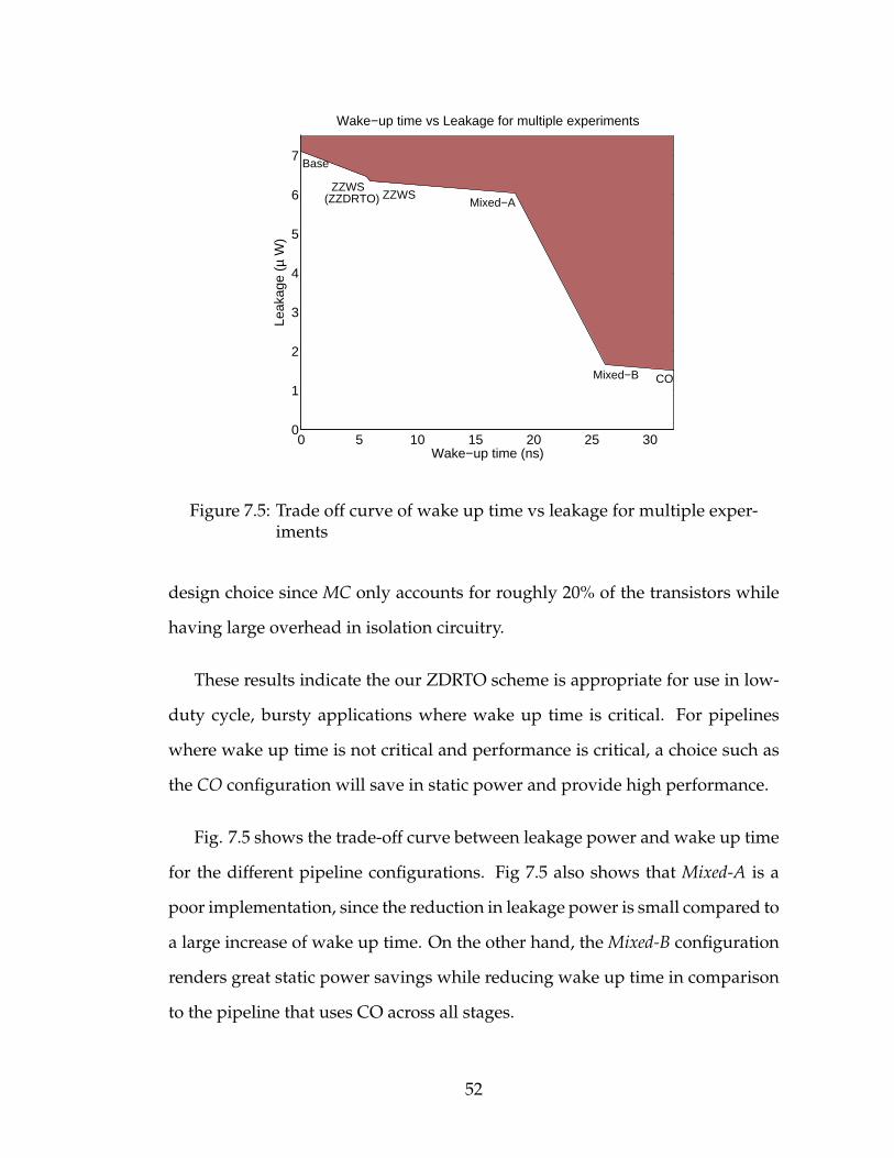
0 5 10 15 20 25 300
1
2
3
4
5
6
7
Wake−up time (ns)
Leak
age
(µ W
)
Base
ZZWS(ZZDRTO) ZZWS
Mixed−A
Mixed−B CO
Wake−up time vs Leakage for multiple experiments
Figure 7.5: Trade off curve of wake up time vs leakage for multiple exper-iments
design choice since MC only accounts for roughly 20% of the transistors while
having large overhead in isolation circuitry.
These results indicate the our ZDRTO scheme is appropriate for use in low-
duty cycle, bursty applications where wake up time is critical. For pipelines
where wake up time is not critical and performance is critical, a choice such as
the CO configuration will save in static power and provide high performance.
Fig. 7.5 shows the trade-off curve between leakage power and wake up time
for the different pipeline configurations. Fig 7.5 also shows that Mixed-A is a
poor implementation, since the reduction in leakage power is small compared to
a large increase of wake up time. On the other hand, the Mixed-B configuration
renders great static power savings while reducing wake up time in comparison
to the pipeline that uses CO across all stages.
52

CHAPTER 8
DISCUSSION
This novel work presents the required conditions and requirements to imple-
ment different power gating techniques in the context of asynchronous circuits.
Our experiments show that our Zero-Delay Ripple Turn On (ZDRTO) tech-
nique reduces the penalty of waking up a pipeline from sleep mode while re-
ducing the static power consumption between 20% and 80%. Furthermore our
results show the trade offs between static power reduction savings and wake
up time.
The CO technique offers an average of 80% of static power savings. One the
other hand, the transient behavior of the CO technique might cause undesir-
able dynamic behavior. We require a deeper analysis to determine how these
transient effects affect the overall power consumption. We plan to extend this
work to quantitatively define the Break Even Point (BEP), that is minimum time
a circuit must be idle such that the average power consumption is reduced.
We also plan to develop in the future a tool to automatically cluster pipeline
stages and to chose the best power technique for each cluster given the static
power requirements and maximum allowed wake up time.
53

CHAPTER 9
CONCLUSION
Static power is a primary design parameter that circuit engineers need to con-
sider when designing circuits that have low-duty cycle and run on unreliable
and short-lived sources of power like batteries or solar cells. This work presents
the scenarios that yield leakage currents and the most common techniques to
abate these parasitic currents at the device, circuit, and system level. Digital
circuits can benefit by significant static power savings from system wide tech-
niques, specially those that can be applied systematically independent of the
design: clock gating and power gating. Asynchronous circuits already imple-
ment the equivalent of a fine-grain clock gating design but further static power
savings can be obtained by exploiting power gating techniques.
This work presents for the first time an implementation and evaluation of
different power gating schemes in the context of asynchronous circuits. Zig-
Zag Cut-Off (ZZCO) power gating offers fast wake up time, but only reduces
static power by 30% on average. Cut-Off (CO) power-gating offers an aver-
age of 80% power savings, at the cost of increased complexity and the need
for careful timing analysis. We offer an example analysis and evaluation of
power gating applied to an asynchronous AES encryption/decryption pipeline
as well as a generic empty pipeline detection technique to be incorporated into
power gating control circuitry with minimum area, power, and performance
overheads. Finally, we introduce a novel Zero-Delay Ripple Turn On (ZDRTO)
technique to reduce the penalty of waking up a pipeline from sleep mode. Fur-
thermore, we present ZDRTO using hybrid power gating schemes in order to
exhibit the trade-offs between maximum static power savings and minimum
wake up time.
54

BIBLIOGRAPHY
[1] Manohar Rajit Akopyan, Filipp, Otero, Carlos, Fang, David, Jackson San-dra. Variability in 3-D integrated circuits. In Custom Integrated CircuitsConference, pages 659–662, 2008.
[2] K.M. Cao, W.-C. Lee, W. Liu, X. Jin, P. Su, S.K.H. Fung, J.X. An, B. Yu,and C. Hu. Bsim4 gate leakage model including source-drain partition. InIEDM Technical Digest, pages 815–818, 2000.
[3] Anantha P Chandrakasan and Robert W Brodersen. Low Power DigitalCMOS Design. Kluwer Academic Publishers, Norwell, MA, USA, 1995.
[4] Yang-Kyu Choi, Daewon Ha, Tsu-Jae King, and Jeffrey Bokor. Investiga-tion of Gate-Induced Drain Leakage (GIDL) Current in Thin Body Devices:Single-Gate Ultra-Thin Body, Symmetrical Double-Gate, and Asymmetri-cal Double-Gate MOSFETs. Japanese Journal of Applied Physics, 42(Part 1,No. 4B):2073–2076, 2003.
[5] Mark E. Dean, David L. Dill, and Mark Horowitz. Self-timed logic usingcurrent-sensing completion detection (cscd). J. VLSI Signal Process. Syst.,7(1-2):7–16, 1994.
[6] B S Deepaksubramanyan and A Nunez. Analysis of subthreshold leakagereduction in CMOS digital circuits. In Circuits and Systems, 2007. MWSCAS2007. 50th Midwest Symposium on, pages 1400–1404, 2007.
[7] J Ebergen and A Peeters. Design and analysis of delay-insensitive modulo-n counters. Formal Methods in System Design, 3(3):211–232, Jan 1993.
[8] FIPS. Advanced Encryption Standard (AES). pub-NIST, pub-NIST:adr, 2001.
[9] R H Fowler and L W Nordheim. ”Electron emission in intense electricfields”. Proc R. Soc. London, Ser. A, vol. 119(781):173, 1928.
[10] Fatih Hamzaoglu and Mircea Stan. Circuit-level techniques to control gateleakage for sub-100nm cmos. ACM ISLPED, Aug 2002.
[11] M Horiguchi, T Sakata, and K Itoh. Switched-source-impedance cmos cir-cuit for low standby subthreshold current giga-scale lsi’s. IEEE VLSIC,pages 47 – 48, May 1993.
55

[12] M Imai, K Takada, and T Nanya. Fine-grain leakage power reduc-tion method for m-out-of-n encoded circuits using multi-threshold-voltagetransistors. IEEE ASYNC, pages 209 – 216, May 2009.
[13] T Inukai, M Takamiya, K Nose, H Kawaguchi, T Hiramoto, and T Sakurai.Boosted gate mos (bgmos): device/circuit cooperation scheme to achieveleakage-free giga-scale integration. IEEE CICC, pages 409 – 412, May 2000.
[14] J Kao, A Chandrakasan, and D Antoniadis. Transistor sizing issues andtool for multi-threshold cmos technology. DAC, pages 409 – 414, Jan 1997.
[15] H Kawaguchi, K Nose, and T Sakurai. A super cut-off cmos (sccmos)scheme for 0.5-v supply voltage with picoampere stand-by current. IEEESSC, 35(10):1498 – 1501, Oct 2000.
[16] A Keshavarzi, K Roy, and C Hawkins. Intrinsic leakage in low power deepsubmicron cmos ics. IEEE ITC, pages 146 – 155, Nov 1997.
[17] J Kessels. Calculational Derivation of a Counter with Bounded Response Time,volume 683/1993. Jan 1993.
[18] S Kim, S Kosonocky, and D Knebel. Understanding and minimizingground bounce during mode transition of power gating structures. IEEEISLPED, pages 22 – 25, Aug 2003.
[19] T Kuroda, T Fujita, T Nagamatu, S Yoshioka, T Sei, K Matsuo, Y Hamura,T Mori, M Murota, M Kakumu, and T Sakurai. A high-speed low-power0.3 m cmos gate array with variable threshold voltage (vt) scheme. IEEECICC, pages 53 – 56, May 1996.
[20] Tong Lin, Kwen-Siong Chong, Bah-Hwee Gwee, and J Chang. Fine-grained power gating for leakage and short-circuit power reduction by us-ing asynchronous-logic. IEEE ISCAS, pages 3162 – 3165, May 2009.
[21] Alain J. Martin. Compiling communicating processes into delay-insensitive VLSI circuits. Distributed Computing, 1(4):226–234, December1986.
[22] Kyeong-Sik Min and T Sakurai. Zigzag super cut–off cmos (zsccmos)scheme with self–saturated virtual power lines for subthreshold–leakage–suppressed sub–1–v–vddlsi’s. IEEE ISSCC, pages 679 – 682, Sep 2002.
56

[23] S. Mukhopadhyay, C. Neau, R.T. Cakici, A. Agarwal, C.H. Kim, and K. Roy.Gate leakage reduction for scaled devices using transistor stacking. IEEETransactions on Very Large Scale Integration (VLSI) Systems, 11(4):716–730,Aug. 2003.
[24] S Mutoh, T Douseki, Y Matsuya, T Aoki, S Shigematsu, and J Yamada. 1-vpower supply high-speed digital circuit technology with multithreshold-voltage cmos. IEEE SSC, 30(8):847 – 854, Aug 1995.
[25] Siva Narendra, Vivek De, Dimitri Antoniadis, Anantha Chandrakasan, andShekhar Borkar. Scaling of stack effect and its application for leakage re-duction. In Proceedings of the 2001 international symposium on Low powerelectronics and design - ISLPED ’01, pages 195–200, New York, New York,USA, August 2001. ACM Press.
[26] Scott Thompson Portland. MOS Scaling: Transistor Challenges for the 21stCentury.
[27] Rahul M Rao, Richard B Brown Kevin Nowka, and Jeffrey L Burns. Analy-sis and mitigation of CMOS gate Leakage.
[28] C. Riccobene. Limits of gate-oxide scaling in nano-transistors. In 2000 Sym-posium on VLSI Technology. Digest of Technical Papers (Cat. No.00CH37104),pages 90–91. IEEE.
[29] K Roy, S Mukhopadhyay, and H Mahmoodi-Meimand. Leakage cur-rent mechanisms and leakage reduction techniques in deep-submicrometercmos circuits. Proc. IEEE, 91(2):305 – 327, Feb 2003.
[30] K Roy, S Mukhopadhyay, and H Mahmoodi-Meimand. Leakage cur-rent mechanisms and leakage reduction techniques in deep-submicrometerCMOS circuits. Proceedings of the IEEE, 91(2):305–327, February 2003.
[31] K Shi and D Howard. Sleep transistor design and implementation - simpleconcepts yet challenges to be optimum. IEEE VLSI-DAT, pages 1 – 4, Apr2006.
[32] Youngsoo Shin and Hyung-Ock Kim;. Cell-based semicustom design ofzigzag power gating circuits. IEEE ISQED, pages 527 – 532, Mar 2007.
[33] Ho-Jun Song. A self-off-time detector for reducing standby current ofdram. IEEE SSC, 32(10):1535–1542, 1997.
57

[34] G Tellez, A Farrahi, and M Sarrafzadeh. Activity-driven clock design forlow power circuits. ICCAD, pages 62 – 65, Nov 1995.
[35] Y Thonnart, E Beigne, A Valentian, and P Vivet. Automatic power regu-lation based on an asynchronous activity detection and its application toanoc node leakage reduction. IEEE ASYNC, pages 48–57, 2008.
[36] Yannis Tsividis. Operation and Modeling of the MOS Transistor. Oxford Uni-versity Press, USA, 2 edition, June 2003.
[37] Johannes Wolkerstorfer, Elisabeth Oswald, and Mario Lamberger. An asicimplementation of the aes sboxes. In CT-RSA: Cryptographer’s Track at theRSA Conference on Topics in Cryptology, pages 67–78. Springer-Verlag, 2002.
58