status of adf system design november 2002evans/l1cal/meetings/... · 2002-11-12 · status of adf...
TRANSCRIPT

Status of ADF System DesignNovember 2002
D. Calvet
DSM/DAPNIA/SEDI, CEA Saclay
91191 Gif-sur-Yvette Cedex

[email protected] 2 Saclay, 4 November 2002
Content• Algorithm and Simulation
• Analog Splitters
• ADF board
• ADF crate
• Timing card
• Test bench
• Software
• Summary

[email protected] 3 Saclay, 4 November 2002
ADF System1280 cables (differential analog data) from BLSs
• 32 analog channels + 3 (ou 1?) output 2 Gbit/s per ADF board• 20 ADF boards+ 1 interface per crate (« VME Interconnect »)• 80 ADF boards in 4 VME crates in total• 1 board for timing distribution
Crate 1ADF 20-39
VME
Crate 2 ADF 40-59
VME
Crate 0ADF 0-19
VME
Crate 3 ADF 60-79
VME
Timing
VME
MV
EMV
EMV
E
VME
TAB 0-7GAB
Timing 60 x 2 Gbit/s60 x 2 Gbit/s
CPU
60 x2 Gbit/s
60 x 2 Gbit/sSCL
SCLTriggerControlComputer
L1 framework, L2/DAQ

[email protected] 4 Saclay, 4 November 2002
Trigger Pickoff Signal
396 ns
132 ns
Measuredon one EMchannel
• Rise time too long for operation at 132 ns:Let E=energy deposited for BC #N: 75% of E observed at BC #N-1: can cause fake
trigger at BC #N-1 that causes a veto for BC #N which is lost!
• Long tail: 80% of max after 132 ns; 20% after 396 ns-> Digital Signal Processing

[email protected] 5 Saclay, 4 November 2002
Algorithm• Algorithm unchanged since Nov. 2001 studies• Close to what is done in other experiments:
– ATLAS and CMS: 5 tap FIR @ BC frequency + 3 point peak detector + some logic for saturated pulses
– Proposal for D0: up to 8-tap FIR @ BC x 2 frequency + 3 point peak detector
-> very conservative wrt rate and number of taps
2 8 TapFIR
3 PointPeak
Detector2
ETLook Up
TableADC
10 bit30.28 MHz
Serializer
10 bit15.14 MHz
11 bit15.14 MHz
11 bit7.57 MHz
8 bit7.57 MHz
• VHDL coding completed and simulated• 8 channels fitted in FPGA Xilinx Virtex II 500K gates 456 pins

[email protected] 6 Saclay, 4 November 2002
Simulation Chain
• Largest part of software operational• Some improvements to make; work on coherence with VHDL
simulation results
TriggerPickoffMeasure-ments
Smooth
Filter
ArbitraryWaveformGenerator
SimulatedEnergies
Generator SamplingQuantization
SignalProcessingFilter
Post-proc.Display
Analysis,Validation
DecimationPeriodizationAmplitude scaling,Noise, delay,jitter, pile-up…
Anti-aliasing
Period TN levels
FIR, IIR,other…Floating point,Fixed, precision…
ADFPrototype FPGA
Eval. kitHardware
Software VHDLSimulation

[email protected] 7 Saclay, 4 November 2002
Analog Signal Splitter Card
CTFE CTFECTFE
Trigger L1 calorimeter Run IIa (in operation )
Analog SignalSplitter Card
• Active board for duplicating differential analog signals from 8 trigger towers– Collecting raw data samples– Test of ADF board prototype in parasitic mode
PrototypeADFCables
from BLS

[email protected] 8 Saclay, 4 November 2002
Analog Splitter• One board cabled
• Minor error found:- DC/DC converter need to be soldered on other side of PCB due to
top/bottom view inversion- Missing thermal drain below operational amplifiers-> Corrected PCB not mandatory but will be done
• Test bench- quickly made differential source (AD829), cables and adapted loads
• Preliminary tests (sinus input)- Connector pinout is correct, all channels work; gain is correct- Bandwidth: over 10 MHz
• More tests needed
- arbitrary waveform generator
• Schedule for installation in D0?

[email protected] 9 Saclay, 4 November 2002
ADF Board Status• Core FPGA (digital filter)
– VHDL coding 100% completed and simulated– 8 channels synthetized, fitted in XC2V500 FG456 -4– Post-route simulation done
• VME interface and bootstrap interface– VHDL coding 100% completed and simulated– Programmable logic fitted in XC9572XL –10 TQ100C CPLD
• Board-level VHDL simulation– Includes 4 FPGA’s + VME interface + bootstrap logic– Started for behavioral model– Some control software was developped to exercice the VHDL model-> Several errors in the FPGA logic were found and are being corrected
• Schematic capture: will start in November 2002, although board level simulations not 100% completed- Aim for PCB designed ~end January 2003

[email protected] 10 Saclay, 4 November 2002
ADF board Block Diagram
ChannelLink
serializer
FPGA #1Channel(8-15)
ChannelLink
serializerCLK
VME interface
JTAG
ADCs
FPGA #0Channel(0-7)
FPGA #2Channel(16-23)
FPGA #3Channel(24-31)
FPGAProgrammation
Interface
ChannelLink
serializer
Config.SPROM
808
ADC driversZ DAC
3
8 analog input (J2)
ADCs808
ADC driversZ DAC
8 analog input (J2)
Idem #2808
64 MHz
Idem #3808 36
36
36
32
4Parity #1,
#2, #3
Channel data
ParityBX countStart of frameFrame 8-10 bit
Backplane (J1 reserved pins) SCL interface cable (J0)
24
VME Bus (J1)
3.3 V
1.5 V
3.3 V
-5 V
5 V
1 31
(J0)

[email protected] 11 Saclay, 4 November 2002
ADF Channel Analog Section
• Design in progress…:– Digitization with 10-bit precision, identical input range for all channels – Passive RC filter for anti-aliasing; Octal DAC MAX5307 for zero adjust

[email protected] 12 Saclay, 4 November 2002
ADF Channel Digital Section
InputDecimator
InputSelector
Magnitudecomparator
Convolver Peakdetector
EtLUT
8-bitserializer
SELECTLFSR
constant
Historybuffer
Historybuffer
Historybuffer
10-bitserializer
delay Self trigger
ADCclock
Configuration registers Bus interface Shared signals
Address, RD/WR*Data In, Data Out
out
Channel #N
ADC#N
Common logic
• Logic duplicated for each channel + common logic for channels within the same FPGA

[email protected] 13 Saclay, 4 November 2002
Input Decimator and ADC Clock
InputDecimator
10Input
samples30.28 Msps
1010
Even samples
Odd samples7.57 Msps
7.57 MspsCE CLK PH
2Enable60.56 MHz Phase selection
ADCCLK
30.28 MHz
CLK CLK* D
Phase selection (0)0° 180°30.28 MHz
DDR register
BC clk(a) ADC clk(a) ADC out(a) odd/even
(a’) odd/even
(b) ADC clk(b) ADC out(b) odd/even
(b’) odd/even
Channel #N
• ADC Clock:– Copy or inverted copy of internal 30.28 MHz clock made with DDR reg.
• Input decimator– Keep 2 samples per BC out of the 4 converted depending on phase selection– 4 possible phase value: phase adjustment 1:8 BC i.e. 16.5 ns– Samples output on 2 parallel stream to interface to dual-branch convolver– Decimation done with constant latency wrt BC clock
0 1 2 3
0 1 2 3
0 21 3
0 21
BC
3

[email protected] 14 Saclay, 4 November 2002
Input Decimator and ADC Clock
• E.g. Phase Selection=0; BC period = 128 ns:– Samples 0, 4, 8, 12, 16 … are selected– Samples 0, 8, 16… on q_even with latency of 0.5 BC wrt rising edge of clk_bc – Samples 4, 12, 20… on q_odd with latency of 0.5 BC wrt rising edge of clk_bc

[email protected] 15 Saclay, 4 November 2002
Convolver8 tap
Shift reg.Selector 18 x 18 bitunsignedmultiplierY
XY
X
AdderAccumulator
10Evensamples
Data outAddress, Data in
8 x 6 bitDPSRAM
8 tapShift reg.Selector 18 x 18 bit
unsignedmultiplierY
XY
X10Evensamples
8 x 6 bitDPSRAM
Coef. bus
Coef. bus
16
16
1719
60.52 MHz
7.57 Msps
7.57 Msps
15.14 Msps
Channel #N
Out
Convolver out readyBus interface Shared Control Logic
• Dual-branch convolver:- faster : 8 tap @ 15.14 MHz (Single branch: ~4-5 tap)- But more work because no IP core. Anyway if Xilinx Coregen IP core:
no generic size in VHDL code, control logic not shareable

[email protected] 16 Saclay, 4 November 2002
Peak Detector Output Decimator
QD Decimator
:2
PeakDetectorOff&
16
60.52 MHz
QD16
A>BA
B
A>BA
B
Load
19
3
MSB
Decimateselection
7.57 MspsOutput
« 0 »
Channel #N
From convolver15.14 Msps
Shared Control Logic Output ready
• 3-point peak detector followed by :2 decimator- Only 16 MSB of convolver output compared to save logic- Peak detector On/Off control- Keep 1 output out of 2 (2 possibilities) with constant latency

[email protected] 17 Saclay, 4 November 2002
Peak Detector Post Divisor
10
K
In
16
2
OR
7.57 MspsOutput
MSB
LSB16-K
Overflow
10MSB
LSB
Channel #N
From peak detector7.57 Msps
Post divisor1, 2, 4 or 8
• Arithmetic right shift for result scaling- Programmable post divisor value: 1, 2, 4 or 8- MSB’s that are lost are OR’ed together to make overflow bit- Stage in combinatorial logic

[email protected] 18 Saclay, 4 November 2002
Et Look Up Table
2K x 8 bitDPSRAM
A_A107.57 Msps
D in/out8
7.57 MspsScaled Peak
Calibrated Et output
A_WR
10
Overflow8
A_A9A_A0
A_D7A_D0
‘0’
60.52 MHz A_CLKB_A10-0 B_D7-0B_WRB_CS
13
Bus interface
Data outAddress, Data in
Channel #N
• Look up table for final Et result- Conversion from 10 bit to 8 bit Et- Arbitrary conversion function (e.g. implement clipping, saturation)- Programmable output value when arithmetic overflow (uses ½ LUT)

[email protected] 19 Saclay, 4 November 2002
Serializer and Latency Adjust
Select
7.57 MspsEt
Parallel loadShift RegisterADC raw data
Serial Out
coarseLatency Adjust
IN 7-08
8
8
8
8LFSR
Constant
Q0 1..32
ProgrammableLength shift register
In Out60.52 Mbps
2 3
Select
IN 9-010
Q0ADC raw data (history)
Serializer source2
Channel #N
• 4 possible sources of data for 8-bit serial stream- 8 MSB of ADC value, Et result, Constant value, pseudo-random value
• Switch to 10-bit frames when sending raw ADC samples• Per channel coarse latency adjust (+0 to +3 BC); common fine
adjust (+1/8 BC to +7/8 BC)
60.52 MHz fine SendrawBus interface
Address, Data in Data out

[email protected] 20 Saclay, 4 November 2002
LFSR16-bit Parallel load Shift Register
Q15
Parallel In 15-0
SIN
XNOR
16
Q14 Q13 Q12 Q11 Q10 Q9 Q8 Q7 Q6 Q5 Q4 Q3 Q2 Q1 Q0LFSR Out8
Channel #N
• 16-bit pseudo-random generator- Per channel programmable seed
• 8 LSB’s can be sent to ADF output serial stream• Common shift enable for inter-channel synchronization
60.52 MHz Shift EnableBus interface
Data outAddress, Data in

[email protected] 21 Saclay, 4 November 2002
History Buffer
InputSelector
Shift R.
DPRAM1024 x 18 bit
SharedLogic
ADC input
Bus interface
ADDR_A
DOUT_A
DIN_A
WR_ACE_A
ADDR_BDOUT_B
DIN_B
WR_BCE_B
Selector Inputdecimator
10
16Test mode
8Et result
Convolveroutput
Out oddOut even
Data outAddress , Data in
WCLK_A
WCLK_B
« 00 »
10
Phaseselection
Phase sel.(0)CLK BCx8
CEPr.
T
Channel #N
• History buffer used for test mode without ADC input:- Play at input of digital filter digital values pre-loaded via bus interface

[email protected] 22 Saclay, 4 November 2002
History Buffer UsageConvolver Out(K-L)
Raw ADC(K)Convolver Out(K-L)
Et(K-L)
Raw ADC(K+1/4)Et(K-L)Convolver Out(K-L+1/2)
Raw ADC(K+1/2)Et(K-L)Convolver Out(K-L+1/2)
Raw ADC(K+3/4)Et(K-L)Convolver Out(K-L+1)
Raw ADC(K+1)Et(K-L+1)
0x0000x001
Memory content shown forfor phase selection = 0 or 2
For phase selection = 1 or 3,the content of odd and evenaddresses is exchanged
0x0020x003
BC #K0x0040x0050x0060x0070x006
BC #K+1 0x007
0x2FF
• Shared 1024 x 18 bit SRAM written at BC x 8- 512 x 10 bit: raw ADC sample (sample change at BC x 4)- 256 (x 2) x 16 bit: convolver output (result change at BC x 2)- 128 (x4) x 8 bit: Et filtered output (result change at BC x 1)

[email protected] 23 Saclay, 4 November 2002
State Machine for raw sample RAM
Frozen
Resuming
RecordingSuspending
Sending
Reset
Resume command
L1 accept,L1 monitoring,L1 self,L1 software
Freeze after send
Resume after send
Do not sendraw ADC dataSend raw
ADC data
Resumecomplete
Send countnot reached
FPGA #0, #1, #2, #3
Resume after send: if L1 accept and none of L1 monitoring, L1 self, L1 software flagsFreeze after send: if any of L1 monitoring, L1 self or L1 software flagsL1 accept, monitoring, self, software are previously ANDed with corresponding mask flag

[email protected] 24 Saclay, 4 November 2002
BX and Turn Count Serializer
16-bitup counter
Reset
ClkQ
Init ReqGeo. section
1-159up counter
Preset ‘1’
ClkQ
BX Marker=159
7.57 MHz
30-bit// loadShift
register
16
8’00’
’00’
8
8
’00’
30
Q0
Load
Latency Adjust
1..32
ProgrammableLength shift register
In Out
2 3coarse
FPGA #0, #1, #2, #3
SerialBX/TC
60.52 Mbps
60.52 MHz fine
• When sending 8-bit frames to TAB:- Load activated every 8 ticks: serial stream is 8-bit current BX count
• When sending 10-bit frames to TAB:- Single shot on load: serial stream is: BX count, 8 LSB of turn count, 8
MSB of turn count; these 3 bytes are put in 10-bit frames (pad: 00)

[email protected] 25 Saclay, 4 November 2002
Last L1 BX and Turn CountReset
Q
Resuming recording Reset
ClkQ
Single shot after Suspending16
8
Last L1Turn Count
Last L1 BX CountD
ClkDTurn Count
BX Count
Bus interface
Data outAddress , Data in
16
8
FPGA #0, #1, #2, #3
• After trigger causing raw sample recording to freeze:- Latch current BX and Turn count- Made available for read via bus interface- Reset occurs when raw sample recording resumes

[email protected] 26 Saclay, 4 November 2002
Parity Generation
XorChannel serial data 8
FPGA #0 only
Xor
BX/TC serial dataFrame_8_10
Frame
Parity output forFPGA #1, #2, #3
Parity output forFPGA #0
Parity out
Parity out #1Parity out #2Parity out #3
• Parity of 8 channel data calculated by FPGA #0, #1, #2, #3- Partial parity of FPGA #1, #2, #3 sent to FPGA #0- FPGA #0 computes global parity over 32 channels and ctrl signals- Global parity sent to TAB over Channel Link

[email protected] 27 Saclay, 4 November 2002
Start Of Frame
• Frame active when LSB of data is present on serial stream

[email protected] 28 Saclay, 4 November 2002
Frame_8_10
• Frame_8_10 low when sending 8 bit frames; high when sending 10 bit frames (sending raw ADC data following L1 Accept)
[email protected] 29 Saclay, 4 November 2002
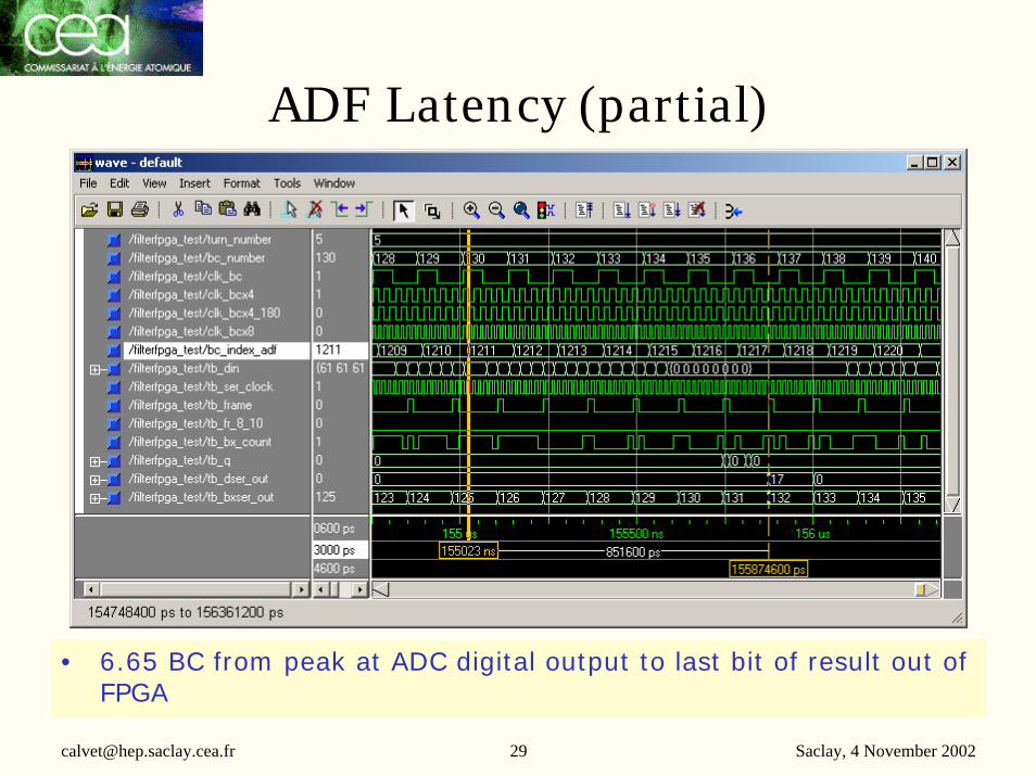
ADF Latency (partial)
• 6.65 BC from peak at ADC digital output to last bit of result out of FPGA

[email protected] 30 Saclay, 4 November 2002
Channel Link Interface
Channel serial data 8FPGA #1
Channel serial data 8FPGA #2
Channel serial dataFPGA #3 8
Channel serial data 8
FPGA #0
Start Of FrameFrame_8_10
BX/TCParity
CLK60.52 MHz
DC BalanceDS_OPT
Driving logic to be defined
DDR
(32+4) x 60.52 Mbps= 2.17872 Gbps
• 36 bit lanes used (out of 48 available):- 8 channel data from by FPGA #0, #1, #2 and #3; 4 control lanes
• Clock + DC balance control bit + option bit

[email protected] 31 Saclay, 4 November 2002
VME interface and bootstrap logic
CY7C960AVME Slave
InterfaceDigital Filter
FPGA’s
74ABT543
74LVC245
XC9572CPLD
A23-A1
D15-D0
XC17S05SPROM
JTAG
D15-D0
D15-D8
PROG_B0..3
DBE3-DBE0
WR/RD*
CS0*-CS3*
LACK*A15-A2
A23-A16DTACK*AS*
DS1*-DS0*AM
WRITE*
C_CS_B0..3C_RD_WR*C_CLK
INIT_BDONE
Slot ID 5-0
VMEBUS
BUSY
74LVC373
• Download FPGA configuration via VME:- all 4 FPGA’s loaded at once or different config on each FPGA
• VME interface A24 D16-D8 only; no DMA; no interrupt• Provides 5V <-> 3.3V conversion; Virtex 2 I/O not 5V tolerant

[email protected] 32 Saclay, 4 November 2002
Types of L1 Trigger for ADF System
• D0 Framework L1 Accept– Generated by D0 framework; sent to all Geographic Sections via SCL– Fanout to ADF system by SCL Interface Fanout card (SCLIF)– Indicates that current BC is a L1 accepted event
• L1 Accept with Monitoring– Generated asynchronously by TCC to indicate that monitoring data of
Geo section should be kept for one of next D0 framework L1 Accept– Sent synchronously by D0 L1 framework to Geo section by L1 Qualifier– If L1 Framework accept and L1 Qualifier for Monitoring asserted: the
current L1 is to be monitored; all history data kept for TCC readout– L1 accept with monitoring flags are fanout to ADF system by SCL
Interface Fanout Card

[email protected] 33 Saclay, 4 November 2002
Types of L1 Trigger for ADF System
• L1 Software Accept– Generated asynchronously by TCC to indicate that one of the next L1
crossing should be treated as D0 Framework L1 Accept by ADF system– Issued by one ADF card upon asynchronous write by TCC,– bounced-back synchronously to ADF system by SCLIF card
• L1 Self trigger Accept– Generated by each ADF channel when ADC input greater than
programmable threshold– Wired-Ored for all channels on an ADF card– Wired-Ored for all ADF cards within each ADF crate and sent to SCLIF– OR-ed by SCLIF and sent back to all ADF cards synchronously
[email protected] 34 Saclay, 4 November 2002
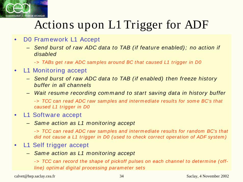
Actions upon L1 Trigger for ADF• D0 Framework L1 Accept
– Send burst of raw ADC data to TAB (if feature enabled); no action if disabled-> TABs get raw ADC samples around BC that caused L1 trigger in D0
• L1 Monitoring accept– Send burst of raw ADC data to TAB (if enabled) then freeze history
buffer in all channels– Wait resume recording command to start saving data in history buffer
-> TCC can read ADC raw samples and intermediate results for some BC’s that caused L1 trigger in D0
• L1 Software accept– Same action as L1 monitoring accept
-> TCC can read ADC raw samples and intermediate results for random BC’s that did not cause a L1 trigger in D0 (used to check correct operation of ADF system)
• L1 Self trigger accept– Same action as L1 monitoring accept
-> TCC can record the shape of pickoff pulses on each channel to determine (off-line) optimal digital processing parameter sets

[email protected] 35 Saclay, 4 November 2002
Limitations• History buffer common for sending raw ADC samples to TAB and
for read-out via TCC– When recording is frozen (i.e. TCC read-out in progress), sub-sequent
L1 accept will not trigger sending of raw ADC samples to TAB-> Raw ADC samples for these L1 accept are lost (but digital filter output continues to flow)
- If no L1 Monitoring or L1 software accept are issued, raw sample recording is never frozen, raw samples for all L1 accept can be sent to TAB
• Links to send filtered data and raw ADC data to TAB are the same – While sending out raw ADC data to TABs, flow of filtered data is
stopped -> can introduce dead-time for L1 if sending time is larger than that of other sub-systems
-> e.g. sending raw samples of 8 BC around L1: 320 bit / channelsending time = 5.28 us

[email protected] 36 Saclay, 4 November 2002
SCL signals fanoutADF#1
ADF#20
ADF#10
ADF#1
ADF#20
ADF#10
SCLReceiver
Mezzanine
SCLInterfaceFanoutCard
(SCLIF)
SCL
ADF
1
ADF#20
ADF#10
8 pairs Crate #0 Crate #1
Crate #2 Crate #31-2 spareADF#1
ADF#20
ADF#10
#
5-6 cables ~3 m;2 mm HM connector
8 pairs; LVDS
ADF board for intra-crate fanout
• 1 cable to one ADF board in each ADF crate• ADF board where cable is plugged in charge of fanout within crate

[email protected] 37 Saclay, 4 November 2002
SCL Interface and Fanout card
• Baseline: segmentation 0.2 x 0.2
SCLReceiver
Mezzanine
(FNAL)
FPGA
4-6 Cables to ADF crate• VHDL design in progress• 3U or 6U mechanics; No slow control• No slot available in ADF crate -> back of slot 0 if enough space
J1 J2
HM 2 mm connector
PROM
logic
configuration
SCL Fiber/Cable

[email protected] 38 Saclay, 4 November 2002
SCLIF to ADF communication• SCLIF to ADF cable pinout (preliminary)
Cable detect rem,loc - GND - BC ClockCMDD (SCLIF->ADF) - GND - CMDU (ADF->SCLIF)BUSY (ADF->SCLIF) - GND - Self Trigger (ADF->SCLIF)ERROR (ADF->SCLIF) - GND - SPARE
Cable detect remote: wired to GND on SCLIF card; pullup resistor on ADF cardCable present local: pullup resistor on SCLIF card; active low output of ADF logic
• CMDD: Command Downstream (SCLIF to ADF system)
8 bit per BC (60.56 Mbit/s link)7 6 5 4 3 2 1 0
Geographic Section Init RequestResume ADC raw sample recordingSofware L1 AcceptSelf generated L1 AcceptL1 Accept for MonitoringD0 Framework L1 AcceptBX MarkerUnused

[email protected] 39 Saclay, 4 November 2002
SCL to ADF communication (con’t)• CMDU: Command Upstream (ADF to SCLIF system)
8 bit per BC (60.56 Mbit/s link)7 6 5 4 3 2 1 0
Geographic Section Init AcknowledgeResume ADC raw sample recordingSofware L1 AcceptUnused
Bits « Resume ADC raw sample recording » and « Sofware L1 Accept »:- Issued by one ADF card upon Write action by TCC to appropriate register-Bounced-back by SCLIF to all ADF crates and cards
-> Equal-delay path from TCC to all ADF cards
Bit « Self L1 Accept »:- Wired-OR self trigger signal for all ADF card within the same crate- Per crate Self Trigger signal send on cable wires to SCLIF- All per crate self trigger signals OR-ed by SCLIF to make Self Trigger bit- Self trigger bit sent to all ADF simultaneously in CMDD serial stream

[email protected] 40 Saclay, 4 November 2002
Intra ADF crate Signal Distribution
SCLIF Cable(to one ADFboard per crate)
(FPGA #0, #1, #2, #3)(FPGA #0, #1, #2, #3)
(FPGA #0, #1, #2, #3)
(CDCV304)
(FPGA #0)
CMDDCLK BC
CMDUBUSY
CLK_BC_BUS_OUT
ERROR
CMDD(7..0)_BUS_OUT
ERROR_BUS_IN
Self Trigger
BUSY_BUS_IN
Remote cable presentLocal cable present
Self trigger BUS_IN
(373)CMDD(7..0)_BUS_IN
CLK_BC_BUS_IN
CMDD(7..0)_BOARD_OUT
CLK_BC_BOARD_OUT
CLK_BC_INCMDD_IN(7..0)
BUSY_BUS_OUTSelf trigger BUS_OUTERROR_BUS_OUT
ADF Board #N
Serial to //RJ0/J0
• ADF board where SCLIF cable plugged: makes fanout of signalson backplane; other ADF boards tri-states outputs to bus• All ADF boards get signals from backplane; local fanout for 4 FPGA’s
P1
VME 64 P1(reserved)bussed lines


[email protected] 42 Saclay, 4 November 2002
FPGA Internal Clock Generation
Digital ClockManager
#1CLK_IN
CLK FX
CLK FX_180
CLK_FB 30.28 MHz , phase = 0°
30.28 MHz , phase = 180°
Digital ClockManager
#2CLK_IN
CLK FX
CLK FX_180
CLK_FB 60.56 MHz , phase = 0°
60.56 MHz , phase = 180°FPGA #0, #1, #2, #3
7.57 MHzOn boardFanout chip
• On-chip BC clock multiplication by 4 and 8• All logic driven at BC x 8 = 60.56 MHz• ADC clock from clock at BC x 4 = 30.28 MHz

[email protected] 43 Saclay, 4 November 2002
System wide BC Clock phase align
SCLMezz.
SCLIF
CLK_BC
Programmabledelay line
FPGA
ADF Crate
clk clk
clkclk2
3
4
5
6
7 8
9
Back-planebus
cable
ADF #20
ADF #1
earliesttower
7.57 MHz
• Clock distribution: expected delay dispersion: ~3 ns; jitter: 400 ps?• Programmable delay line on SCLIF clock: adjusted so that all analog
peaks at ADC input fall within same BC period
1
latesttower
~70 ns
Analog ADC input
BC clock at FPGA

[email protected] 44 Saclay, 4 November 2002
ADF Crate20 ADF boards VME Interface VME64 backplane
Power SupplyFan unit
Custom backplane
ADFBoard(6U)
J1
J0
J2
1timingcable
60 (20?)TABscables
320BLSscables
Rear-side Right view• Crate to be delivered ~November 2002• Custom backplane: design not started

[email protected] 45 Saclay, 4 November 2002
Custom Backplane
External Side:20 x 16
AMP 8 pointsconnectors
option withJ0 transitionconnector
Internal Side:20 VME 160 points
connectors
• Passive backplane; controlled impedance traces
• Need some mechanics to hold (heavy) cables

[email protected] 46 Saclay, 4 November 2002
RJ0 Usage (preliminary)1 2 3 4 5 6 7 8 9 0 1 2 3 4 5 6 7 8 9
Signal +Signal -GNDSignal +Signal -
12345
TABLink #1
TABLink #2
TABLink #3
SCLIFCable
• 19 x 5 2 mm Hard Metric connector can accomodate:- 3 cables to TAB each 8 or 10 pairs (if 8-pair cable: GND 5 pins
between each cable)- 1 cable to SCLIF (for one ADF card in each crate)
• Cable to TAB- 8-pair cable could be 7 signals + 1 clock : transmit 7x6=42 bit of
Channel Link (out of 48), altough 36 bits are assigned at this stage- Cable detection feature?
[email protected] 47 Saclay, 4 November 2002
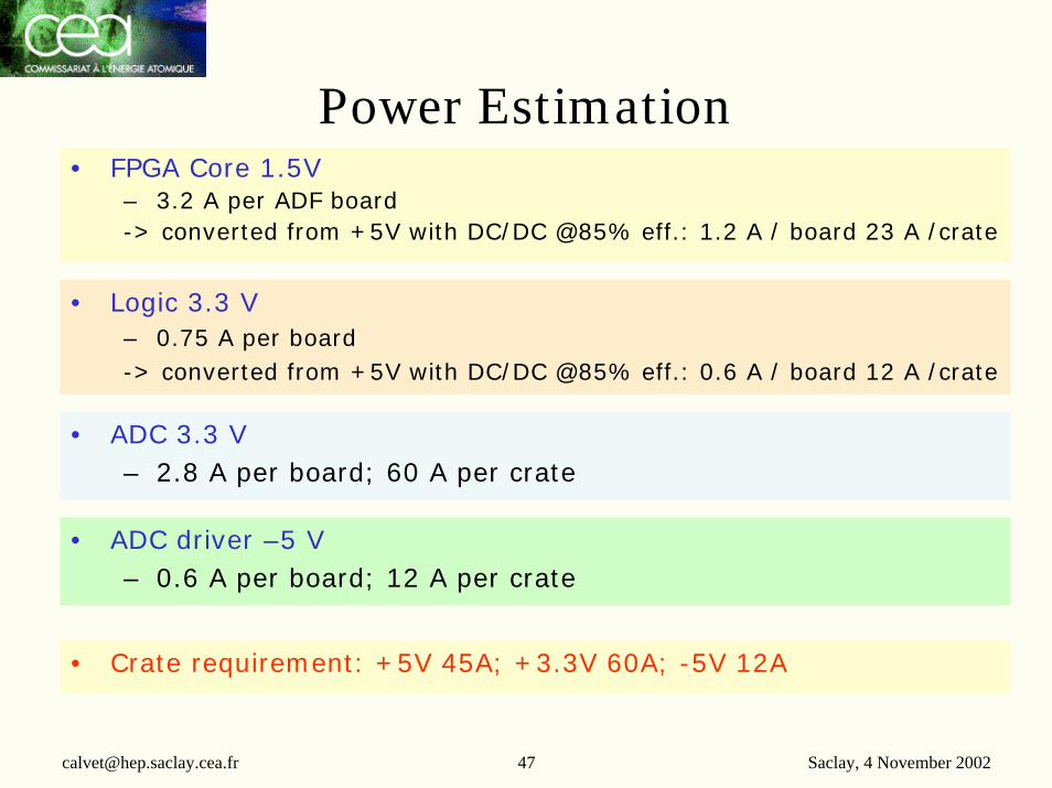
Power Estimation• FPGA Core 1.5V
– 3.2 A per ADF board-> converted from +5V with DC/DC @85% eff.: 1.2 A / board 23 A /crate
• Logic 3.3 V– 0.75 A per board-> converted from +5V with DC/DC @85% eff.: 0.6 A / board 12 A /crate
• ADC 3.3 V– 2.8 A per board; 60 A per crate
• ADC driver –5 V– 0.6 A per board; 12 A per crate
• Crate requirement: +5V 45A; +3.3V 60A; -5V 12A

[email protected] 48 Saclay, 4 November 2002
ADF Power circuitry
2R
• FPGA Core 1.5V– converted from +5V with DC/DC converter EL7564– Per slot startup delay to power each board after the other
16 R+5V
8R 4R R R’
Soft Start
CGeographic address pins0V
• Logic 3.3 V– converted from +5V with DC/DC converter EL7564
• ADC 3.3 V- taken from VME 64 P1 connector
• ADC driver –5 V– taken from VME 64 P1 connector


[email protected] 50 Saclay, 4 November 2002
Test bench ADF board
Evaluation kitFPGA Virtex 2
VME crate
ADF
VMEHigh
Speedcable
PCI/VMEInterface
DeserializerDigitalI/OCard
G Waveformgenerator
PC
Dedicated Mezzanine card
• Standards items + dedicated mezzanine card(s)-> Channel Link de-serializer mezzanine: redundent with Nevis
development-> Mezzanine with 1 ADC (to test 1 analog input + digital filter)

[email protected] 51 Saclay, 4 November 2002
Reduced ADF board6U VME board
Evaluation kitFPGA Virtex 2
DC/DCSerializer
VMEInterface
& bootstrap
ADC
J1
J0
J2
• Debugging VME interface & bootstrap logic• Test DC/DC converter and power supply sequencing• Test 1 serializer with J0/RJ0 PCB traces• Test 1 analog channel
-> Design dependant on time and manpower (e.g. summer student)

[email protected] 52 Saclay, 4 November 2002
Software
• Modular software built in multiple layers- Abstraction of bus interface to support multiple physical
implementation as well as SW/HW co-design with VHDL model- Static libraries for ADF card, crate and system
Bus API
VHDLModelSim
I/O card(Datel)
PCI/VMEInterface Bit3
VMEinterconnect
buslib_VHDL buslib_IO buslib_Bit3 buslib_VMEic
ADF Board libraryADF Crate library
ADF System library
ADF board APIADF Crate API
ADF System API
TCC program
VHDLmodel
Virtex 2Eval. Kit
ADF boardor crate
…
…
…
Bus definitionImplementation
Entitycontrolled
Applicationlayer Test programs
ADF libraries
Physicalinterface

[email protected] 53 Saclay, 4 November 2002
Bus API/* Bus Creation and Deletion functions */
int Bus_Create(BusStruct* *bs, BusArg *ba, char *report, int rep_max, int *rep_sz);
int Bus_Delete(BusStruct* *bs, char *report, int rep_max, int *rep_sz);
/* Bus Open, Close and Control functions */
int Bus_Open(BusStruct* bs, char *report, int rep_max, int *rep_sz);
int Bus_Close(BusStruct* bs, char *report, int rep_max, int *rep_sz);
int Bus_Control(BusStruct* bs, int flags, char *report, int rep_max, int *rep_sz);
int Bus_Sleep(BusStruct* bs, int duration, char *report, int rep_max, int *rep_sz);
/* Bus Read and Write for Byte and Short */
int Bus_ReadByte(BusStruct *bs, unsigned int adr, unsigned char *data, char *report, int rep_max, int *rep_sz);
int Bus_ReadShort(BusStruct *bs, unsigned int adr, unsigned short *data, char *report, int rep_max, int *rep_sz);
int Bus_WriteByte(BusStruct *bs, unsigned int adr, unsigned char data, char *report, int rep_max, int *rep_sz);
int Bus_WriteShort(BusStruct *bs, unsigned int adr, unsigned short data, char *report, int rep_max, int *rep_sz);
• So far, 10 functions defined- At present only one implementation, for VHDL ModelSim simulator

[email protected] 54 Saclay, 4 November 2002
ADF Board API/* ADFboard Creation and Deletion functions */
int ADFboard_Create(...);
int ADFboard_Delete(...);
/* ADFboard Open, Close functions */
int ADFboard_Open(...);
int ADFboard_Close(...);
int ADFboard_ConfigureFPGA(...);
int ADFboard_SetInDecimatorPhase(...);
int ADFboard_SetOutDecimatorPhase(...);
int ADFboard_PeakDetectorOff(...);
int ADFboard_PeakDetectorOn(...);
int ADFboard_SetPeakDivisor(...);
int ADFboard_TestModeOff(...);
int ADFboard_TestModeOn(...);
int ADFboard_SetCoarseLatency(...);
int ADFboard_SetSerializerSource(...);
int ADFboard_SetConstantValue(...);
int ADFboard_SetSelfTriggerThreshold(...);
int ADFboard_SetChannelRegisterA(...);
int ADFboard_SetChannelRegisterB(...);
int ADFboard_RegisterFieldOperation(...);
int ADFboard_RamOperation(...);
int ADFboard_FilterCoefficientOperation(...);
int ADFboard_EnableChannel(...);
int ADFboard_DisableChannel(...);
int ADFboard_GetState(...);
int ADFboard_GetStateAndPrint(...);
int ADFboard_GetClockState(...);
int ADFboard_GetClockStateAndPrint(...);
int ADFboard_GetChipID(...);
int ADFboard_GetChipIDAndPrint(...);
int ADFboard_LoadL1Mask(...);
int ADFboard_SendCommand(...);
...
• At present, about 30 functions defined and implemented- Functions return 0 on success, -1 on error- Printable string contains status of error/success- A function acts on 0 to 32 channels of the ADF card addressed by
appropriate setting of a 32 bit channel selection bit pattern

[email protected] 55 Saclay, 4 November 2002
ADF Crate Address Map
• ADF board selected by VME Slot (Geographical addressing)- 64 KB taken by 4 registers + 256 KB for filter
• 8 MB of address space per crate (~6 MB used)- 4 crates OK with limitation of 32 MB per Bit3 interface
A(22..21) A(20..18) A(17..16) A(15..14)A23 A(13..0) Ressource
11 Slot (2..0) Slot (4..3)
Filter Registers & LUT
FPGA ID00To 11
Slot (4..0)00001
To10100
0 0 Config. A0 1 Config. B
Config. CConfig. D
1 0XX…X
1 1X
XX…X

[email protected] 56 Saclay, 4 November 2002
FPGA Configuration Registers
• All Programmation registers are accessible only in A24/D08
• FPGA Configuration read-back not supported
• Simultaneous download of 4 FPGA’s with same configuration or one different configuration in each FPGA
PROG_B FPGA (3..0) Config. AConfig. BConfig. CConfig. D
Prog. CS_B FPGA (3..0)FPGA configuration DATA (7..0)
WOWO
RegisterD (7..4) D (3..0) Type
WOROBUSY
rsvdDONEINIT_Bx
CLKRD/WR*xxxx RESETxxxx

[email protected] 57 Saclay, 4 November 2002
Filter FPGA Address MapA(15..13) A12 A(6..4)
Channel000To111
0 Et LUT – 2K x 9 bitRAM Addr(10..0)Raw samples – 512 x 10 bitConvol. Out – 256 x 16 bit
Filter Out – 128 x 8 bit
0 0
1 0
0
A(11..10) A(9..7) A(3..1) A0 Ressource
RAM Addr(8..0) 00 1 RAM Addr(8..0) 0
RAM Addr(8..0) 0
1
1 1
0000001
CCC Filter Coef. – 8 x 6 bitXXXXXX
XXX0 LFSR Seed
010 XXXXXX 0 Channel Register AChannel Register B011 XXXXXX 0
100 0 XXXXX 0 Global Register A100 1 XXXXX 0 Global Register B101 0 XXXXX 0 Global Register C101 1 XXXXX 0 Global Register D110 0 XXXXX 0 Global Register E110 1 XXXXX 0 Global Register F

[email protected] 58 Saclay, 4 November 2002
Channel Register A15 14 13 12 11 10 9 8 7 6 5 4 3 2 1 0
Input decimator phase selectOutput decimator phase selectPeak detector: 0: ON; 1: OFFConvolver post-divisorInput selector:
0: external ADC1: raw sample RAM
Coarse latency adjust:00: + 0 BC; 01: +1 BC10: + 2 BC; 11: + 3 BC
Serializer source:00: Filter Et output 01: Constant value register10: LFSR value11: raw ADC sample
Spare

[email protected] 59 Saclay, 4 November 2002
Channel Register B, LFSR Seed
15 14 13 12 11 10 9 8 7 6 5 4 3 2 1 0
Constant value register
Self trigger threshold8 MSB of ADC raw samplescompared to threshold
15 14 13 12 11 10 9 8 7 6 5 4 3 2 1 0
LFSR Seed

[email protected] 60 Saclay, 4 November 2002
Global Register A15 14 13 12 11 10 9 8 7 6 5 4 3 2 1 0
Latency offset count (L)Raw ADC sample RAM operation:- write starts at address 0-read (for send) starts at:
(last_wr_address + L) mod 1024
Fine latency adjust:00: + 0:8 BC; 01: +1:8 BC10: + 2:8 BC; 11: + 3:8 BC
Spare

[email protected] 61 Saclay, 4 November 2002
Global Register B15 14 13 12 11 10 9 8 7 6 5 4 3 2 1 0
Raw ADC sample send burst length (B)-When send:Start: (last_wr_addr + L) mod 1024End: (last_wr_addr + L + B) mod 1024
Send raw ADC sample after L1 accept
Convolver enable
Mask L1 accept; (0 = masked)
Mask L1 monitoring; (0 = masked)
Mask L1 software; (0 = masked)
Mask self L1; (0 = masked)

[email protected] 62 Saclay, 4 November 2002
Global Register C15 14 13 12 11 10 9 8 7 6 5 4 3 2 1 0
Serial DAC CLOCKSerial DAC CS_BSerial DAC Data INSerial DAC Data OUT
Raw sample RAM sequencer state:bit 4: FROZENbit 5: RESUMINGbit 6: RECORDINGbit 7: SUSPENDINGbit 8: SENDING
FPGA chip IDSCL Cable detect (0 = plugged)Generator Clock x 4 LockedGenerator Clock x 8 LockedSpare

[email protected] 63 Saclay, 4 November 2002
Global Register D, E, F15 14 13 12 11 10 9 8 7 6 5 4 3 2 1 0
Reserved (Geo. Section init ack.)Resume ADC raw sample recordingSoftware L1 trigger acceptSpare command bits
Send new command to all ADF’sWhen transition from 0 to 1
Spare
15 14 13 12 11 10 9 8 7 6 5 4 3 2 1 0
Last L1 accept Turn Count
15 14 13 12 11 10 9 8 7 6 5 4 3 2 1 0
Last L1 accept Bunch Crossing Count

[email protected] 64 Saclay, 4 November 2002
Summary• Analog Splitter:
- prototype completed, partially tested -> corrections to PCB coming
• Algorithm and Simulation chain:- Algorithm unchanged: 8 tap FIR @ BCx2 + 3 pt peak detector + LUT- Simulation chain: coherence with VHDL simulation to pursue
• ADF board:- Analog section under design; digital section almost completed- Schematic to start soon; some board level VHDL simulation to do
• Other ADF system components- Crate to be delivered, custom backplane: design not started- SCL timing Fanout board: VHDL design and simulation in progress- Testbench: 2 ideas around Virtex II evaluation kit – no design started
• Software- Some low level functions to control ADF board written and tested- Interface with TCC, D0 DAQ, calibration software: no yet addressed