status of wide bandgap device qualification standards ......mar 08, 2018 · • quick refresher of...
TRANSCRIPT

Status of wide bandgap device qualification standards effort by new
JEDEC committee JC-70
Stephanie Watts Butler, PhD, PEHV Technology Innovation ArchitectTexas Instruments
JEDEC JC-70 Chair
APEC 2018 Industry SessionMarch 8, 2018
Tim McDonaldSenior DirectorGaN Technology Development Worldwide Applications and MarketingInfineon TechnologiesJEDEC JC-70.1 Chair

Abstract
With wide bandgap power products ramping, interest in standards unique to them is also growing. In late 2017, JEDEC launched a new committee (JC-70) chartered to deliver test, datasheet, and qualification standards unique to wide bandgap devices (GaN and SiC). This committee is the final result and home for the previous GaNSPECworking group, which formed at APEC 2016, and its sister group (SiCSPEC), which formed later. This talk will cover the formation of the working group, its transformation into a JEDEC committee, its key challenges and goals, and review progress made to date. The talk will include how attendees can become involved in the work of JC-70 and JEDEC.
2

Agenda
• Quick Refresher of Wide Bandgap Standards Activities in Power Electronics– Launch of GaNSPEC DWG at APEC 2016
• Progress & Path into JEDEC• JEDEC Structure• How to Become Involved with JEDEC
3

March 2014, UCSB Institute for Energy Efficiency Technology Roundtable: Stds for GaN Power Electronics (Mishra, NIST)
History of ~independent WBG activitiesbefore creation of GaNSPEC DWG
4
JEDEC Board of Directors Investigates Future Needs of Industry• Ultimately Issuing Survey Right after APEC 2016
WiPDA at VT Nov 2015, Tim McDonald Presents on GaN Reliability• Generates Several Volunteers for GaN Standards activity to
Tim McDonald & Stephanie Watts Butler
APEC 2015, IEEE PELS Standards Group meets with SiC Focus IEDM 2015, IEEE EDS Holds Discussion:
“Guidelines and Standards for Reliability Testing in Power Electronics” Dec. 2015, IEEE PELS Launches Proposal for International Technology
Roadmap for Wide Bandgap
APEC 2016: Assess Interest & Launch GaNSPEC DWG

Mission of GaNSPEC DWG GaN Standards for Power ElectronicConversion Devices Working Group
We seek to create standards and guidelines for Test and Characterization Methods, Reliability & Qualification Procedures, and Datasheet Elements and Parameters for GaN based power conversion devices
5

Organizational structure
Steering Team
Reliability and Qualification ProceduresCo-Chairs
Datasheet Elements and ParametersCo-Chairs
Test and Characterization
MethodsCo-Chairs
6
Focus teams are self directed and set their own goals and plans but submit their work plans to the steering
team for approval
Liaison:
Steering team provides guidelines/ templates to focus
teams to standardize expectations
Champion

What comes to mind when you hear “JEDEC Qualification”: a typical qualification table
7
• JEDEC offers test methods to support these and other tests. Partial list:– JESD22 A104, Temperature Cycling– JESD22-A101, Steady-State Temperature Humidity Bias Life Test– JESD22 A-108, High Temperature Reverse Bias (HTRB and HTGB)– JESD-A102, Accelerated Moisture Resistance-Unbiased Autoclave.
• But there is much more…..
QU S S Parameter
Part Type Test Conditions Duration measurements @ QuantityPart no “X” TC -55°C/150°C 1000 cy 0/168/500/1000 3 x 77
H3TRB 85°C/85%RH/100V 1000 hrs 0/168/500/1000 3 x 77 HTRB 150°C/960V 1000 hrs 0/168/500/1000 3 x 77 HTGB 150°C/20V 1000 hrs 0/168/500/1000 3 x 77 IOL delta Tj = 100°C 5,000 cy 0/2500/5000 3 x 77 AC 121°C/15psig 96 hrs 0/96 3 x 77
From : “State of Demonstrated HV GaN Reliability and Further Requirements” , T. McDonald, APEC 2015 Industry session

JEDEC JESD94B introductionApplication Specific Qualification Using Knowledge Based Test
8

GaNSPEC DWG approach in JESD94B Lingo
9
MISSION PROFILE
PROCESSING{Methodology}
OUTPUTS:• REL PROCEDURE• TEST METHODS• DATASHEET
PARAMETRICSGaNSPEC DWG GUIDELINES
INPUTS

Test Knowledge:‐ Test Methods for Each Parameter
Datasheet Knowledge:‐ Parameters Important to Application
Types
METHODOLOGYMETHODOLOGY
Knowledge
Methods for Mission
RELKnowledge
‐ Failure Mechanisms
‐ How Use AF‐Which Stress
Methods for Mission
Relational Explanation
IC/FET Supplier
Knowledge of Their Device
IC/FET Supplier
Knowledge of Their Device
MISSION PROFILE-Typical use conditions in the
target applications-Targeted Lifetime/
FIT Rates/MTTF
MISSION PROFILE-Typical use conditions in the
target applications-Targeted Lifetime/
FIT Rates/MTTF
Related Application Standards
Related Application Standards
REL Procedure
Supplierdetermines how to implement
Test Methods
Supplier decides Production/Bench/Characterization
Datasheet Parameters GaN Specific
Items
INPUTSOUTPUTS
10
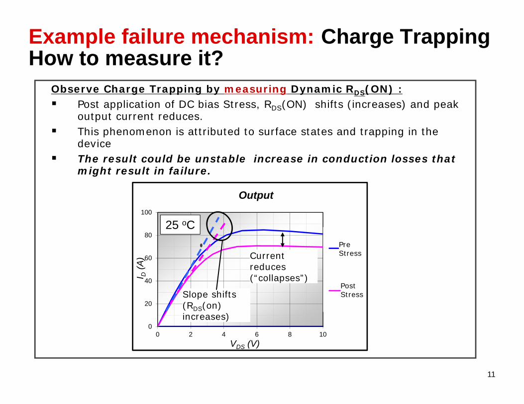
Observe Charge Trapping by measuring Dynamic RDS(ON) : Post application of DC bias Stress, RDS(ON) shifts (increases) and peak
output current reduces. This phenomenon is attributed to surface states and trapping in the
device The result could be unstable increase in conduction losses that
might result in failure.
0
20
40
60
80
100
0 2 4 6 8 10
I D(A
)
VDS (V)
Output
10V
4.5V
25 oC
Slope shifts (RDS(on) increases)
Current reduces (“collapses”)
Pre Stress
Post Stress
Example failure mechanism: Charge TrappingHow to measure it?
1111

12
Normal conduction through 2DEG
Ref: Jones, E.A.; Wang, F.; Ozpineci, B., "Application-based review of GaN HFETs," Wide Bandgap Power Devices and Applications (WiPDA) 2014, pp.24-29, 13-15 Oct. 2014
Initial RDS(ON) reading taken from steady state with full populated two dimensional electron gas (2DEG)
13
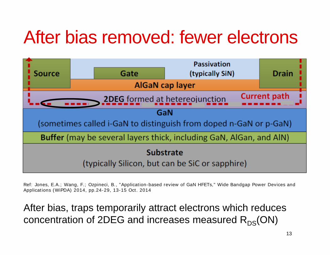
After bias removed: fewer electrons
Ref: Jones, E.A.; Wang, F.; Ozpineci, B., "Application-based review of GaN HFETs," Wide Bandgap Power Devices and Applications (WiPDA) 2014, pp.24-29, 13-15 Oct. 2014
After bias, traps temporarily attract electrons which reduces concentration of 2DEG and increases measured RDS(ON)

14
After time: electrons repopulate 2DEG
Ref: Jones, E.A.; Wang, F.; Ozpineci, B., "Application-based review of GaN HFETs," Wide Bandgap Power Devices and Applications (WiPDA) 2014, pp.24-29, 13-15 Oct. 2014
Steady state can be recovered with time
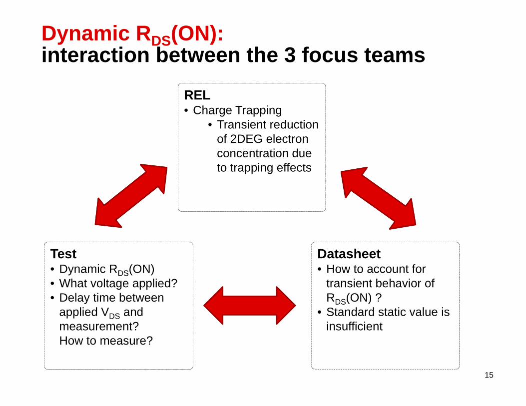
Dynamic RDS(ON): interaction between the 3 focus teams
15
Datasheet• How to account for
transient behavior of RDS(ON) ?
• Standard static value is insufficient
Test• Dynamic RDS(ON)• What voltage applied?• Delay time between
applied VDS and measurement? How to measure?
REL• Charge Trapping
• Transient reduction of 2DEG electron concentration due to trapping effects

Progress
• Getting competitors to work together is a challenge; we had to climb the ladder to overcome obstacles
• Members already had full-time GaN jobs
• Progress sometimes slows or even “slides” back
• Overall cooperation and results have been remarkable!
16
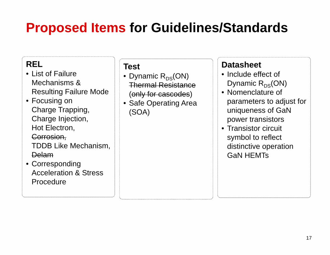
Proposed Items for Guidelines/Standards
17
Datasheet• Include effect of
Dynamic RDS(ON) • Nomenclature of
parameters to adjust for uniqueness of GaN power transistors
• Transistor circuit symbol to reflect distinctive operation GaN HEMTs
Test• Dynamic RDS(ON)
Thermal Resistance (only for cascodes)
• Safe Operating Area (SOA)
REL• List of Failure
Mechanisms & Resulting Failure Mode
• Focusing onCharge Trapping, Charge Injection, Hot Electron, Corrosion, TDDB Like Mechanism, Delam
• Corresponding Acceleration & Stress Procedure

Proposed Items for Guidelines/Standards
18
Datasheet• Include effect of
Dynamic RDS(ON) • Nomenclature of
parameters to adjust for uniqueness of GaN power transistors
• Transistor circuit symbol to reflect distinctive operation GaN HEMTs
Test• Dynamic RDS(ON)
Thermal Resistance (only for cascodes)
• Safe Operating Area (SOA)
REL• List of Failure
Mechanisms & Resulting Failure Mode
• Focusing onCharge Trapping, Charge Injection, Hot Electron, Corrosion, TDDB Like Mechanism, Delam
• Corresponding Acceleration & Stress Procedure

Global Standards for the Microelectronics Industry
• JEDEC has developed standards with industry-wide, international acceptance since 1958.
• JEDEC’s member companies are worldwide and represent a large proportion of the microelectronics industry. – JEDEC partners with other standards groups such as IEC, ANSI, ESDA,
China Electronics Standardization Institute (CESI), JEITA– JEDEC formed its first task groups in China in 2016
• Over 1,000 JEDEC standards and publications serving all segments of the microelectronics industry
• www.jedec.org
19
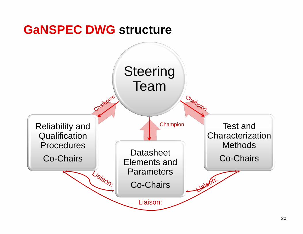
GaNSPEC DWG structure
Steering Team
Reliability and Qualification ProceduresCo-Chairs
Datasheet Elements and ParametersCo-Chairs
Test and Characterization
MethodsCo-Chairs
20
Liaison:
Champion

JEDEC Committee JC-70.1 structure
21
JC-70.1 Subcommittee GaN Power Electronic
Conversion Semiconductor
Standards
Task Group TG701_1GaN Power Electronic
Conversion Semiconductor Reliability and Qualification
Procedures Task Group TG701_2GaN Power Electronic
Conversion Semiconductor Datasheet Elements and
Parameters
Task Group TG701_3GaN Power Electronic
Conversion Semiconductor Test and Characterization
Methods

JC-70 Structure: Wide Bandgap (GaN & SiC)
JC-70 Wide Bandgap Power Electronic Conversion
Semiconductors
JC-70 Wide Bandgap Power Electronic Conversion
Semiconductors
JC-70.1 Subcommittee GaN Power Electronic Conversion
Semiconductor Standards
JC-70.1 Subcommittee GaN Power Electronic Conversion
Semiconductor Standards
JC-70.2 Subcommittee SiC Power Electronic Conversion
Semiconductor Standards
JC-70.2 Subcommittee SiC Power Electronic Conversion
Semiconductor Standards

JC-70 Structure: Scope• The products within scope include discrete devices and integrated circuits that
employ wide bandgap and ultra wide bandgap semiconductors and are intended for use in power conversion circuits regardless of device type, polarity, mode of operation, packaging, electrical ratings, and end applications. This also includes bare die devices and modules that incorporate at least one such bare die device. In addition, the scope includes packaging unique to the products.
• Products intended for use in RF/microwave amplification and signal conditioning applications are generally not covered by this committee, as the operating conditions and performance requirements of these devices are fundamentally different from those of power conversion circuits. Quality and reliability standards for these products are covered by the JEDEC subcommittee JC-14.7.
• The committee is responsible for the development and establishment of industry standards concerned with reliability verification and qualification procedures, test methods and measurement techniques, data sheet elements and device specifications, unique packaging considerations, and other related engineering issues. Activities also include cataloging and consideration of mission profiles, and formulation of terms, definitions, and symbols for the products defined above

JC-70 Structure: Scope• The products within scope include discrete devices and integrated circuits that employ
wide bandgap and ultra wide bandgap semiconductors and are intended for use in power conversion circuits regardless of device type, polarity, mode of operation, packaging, electrical ratings, and end applications. This also includes bare die devices and modules that incorporate at least one such bare die device. In addition, the scope includes packaging unique to the products.
• Products intended for use in RF/microwave amplification and signal conditioning applications are generally not covered by this committee, as the operating conditions and performance requirements of these devices are fundamentally different from those of power conversion circuits. Quality and reliability standards for these products are covered by the JEDEC subcommittee JC-14.7.
• The committee is responsible for the development and establishment of industry standards concerned with reliability verification and qualification procedures, test methods and measurement techniques, data sheet elements and device specifications, unique packaging considerations, and other related engineering issues. Activities also include cataloging and consideration of mission profiles, and formulation of terms, definitions, and symbols for the products defined above
JC-70 Structure: Scope• Products
– discrete devices and integrated circuits – wide bandgap and ultra wide bandgap semiconductors – power conversion circuits regardless of device type, polarity, mode of
operation, packaging, electrical ratings, and end applications.
• RF/microwave amplification and signal conditioning applications are generally not covered
• Industry standards concerned with – reliability verification and qualification procedures, – test methods and measurement techniques, data sheet elements and
device specifications, unique packaging considerations– cataloging and consideration of
mission profiles, and formulation of terms, definitions, and symbols
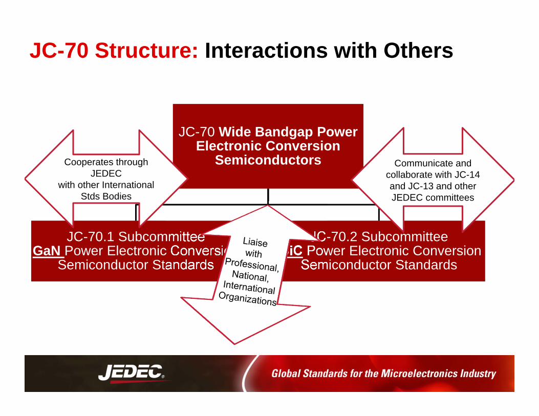
JC-70 Structure: Interactions with Others
JC-70 Wide Bandgap Power Electronic Conversion
Semiconductors
JC-70 Wide Bandgap Power Electronic Conversion
Semiconductors
JC-70.1 Subcommittee GaN Power Electronic Conversion
Semiconductor Standards
JC-70.1 Subcommittee GaN Power Electronic Conversion
Semiconductor Standards
JC-70.2 Subcommittee SiC Power Electronic Conversion
Semiconductor Standards
JC-70.2 Subcommittee SiC Power Electronic Conversion
Semiconductor Standards
Communicate and collaborate with JC-14 and JC-13 and other JEDEC committees
Cooperates through JEDEC
with other International Stds Bodies
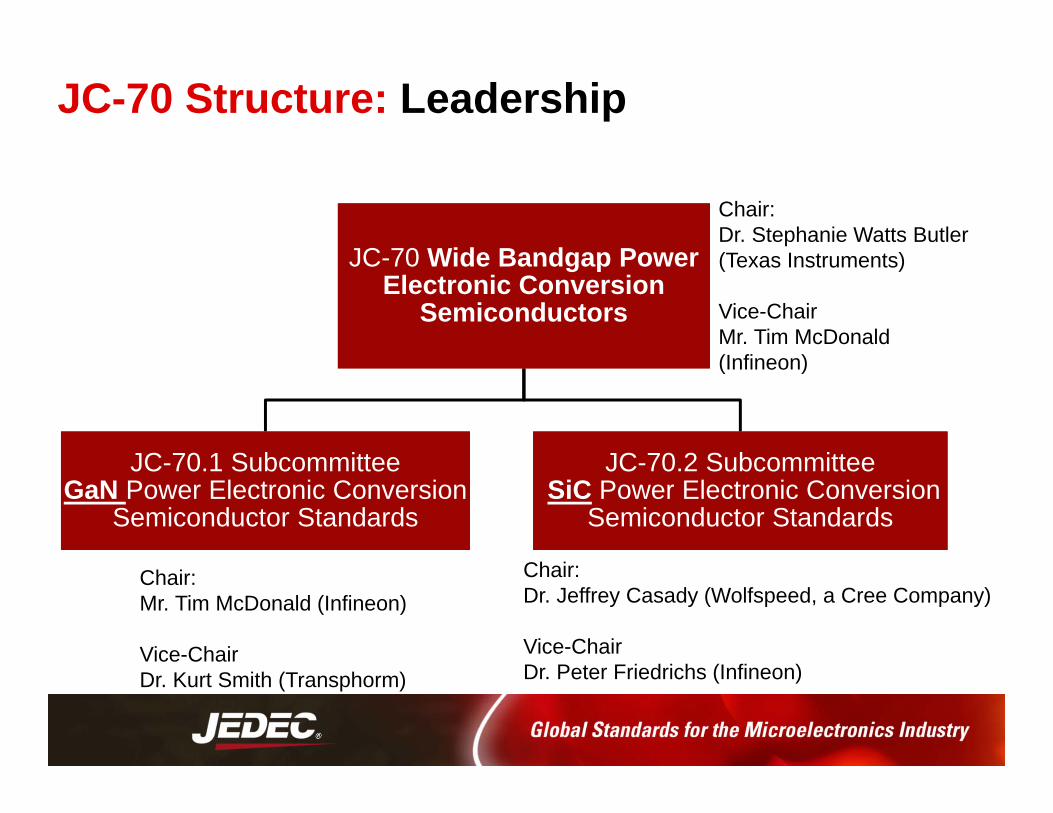
JC-70 Structure: Leadership
JC-70 Wide Bandgap Power Electronic Conversion
Semiconductors
JC-70 Wide Bandgap Power Electronic Conversion
Semiconductors
JC-70.1 Subcommittee GaN Power Electronic Conversion
Semiconductor Standards
JC-70.1 Subcommittee GaN Power Electronic Conversion
Semiconductor Standards
JC-70.2 Subcommittee SiC Power Electronic Conversion
Semiconductor Standards
JC-70.2 Subcommittee SiC Power Electronic Conversion
Semiconductor Standards
Chair:Dr. Stephanie Watts Butler(Texas Instruments)
Vice-ChairMr. Tim McDonald(Infineon)
Chair:Mr. Tim McDonald (Infineon)
Vice-ChairDr. Kurt Smith (Transphorm)
Chair:Dr. Jeffrey Casady (Wolfspeed, a Cree Company)
Vice-ChairDr. Peter Friedrichs (Infineon)

JC-70 Member List• ABB• Accel RF Instruments Corporation• Analog Devices Inc.• Efficient Power Conversion Corp• ExaGan• Freebird Semiconductor Corporation• GaN Systems• General Electric• Hewlett Packard Enterprise Co• Hirex Engineering• Infineon• Intel• Keysight Technologies Inc• Lenovo• M/A-COM Technology Solutions• Mentor, a Siemens Company• Micron Technology Inc• Microsemi Corporation• Monolith Semiconductor Inc
• Navitas Semiconductor• NXP Semiconductors• ON Semiconductor• Panasonic Corporation• Power Integrations• QROMIS Inc• Renesas• Rohm Semiconductor• STMicroelectronics• Sumitomo Electric Industries • Taiwan Semiconductor Mfg Company• Tektronix• Texas Instruments Inc• Transphorm• U.S. Army AMRDEC• Vishay Corporation• VisIC Technologies• Wolfspeed, a Cree Company• Xiamen Sanan Integrated Circuit Co• ZTE Corporation
...and still growing!
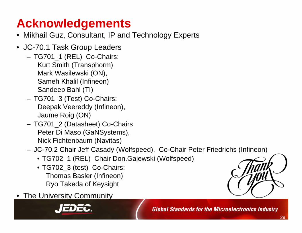
Acknowledgements• Mikhail Guz, Consultant, IP and Technology Experts• JC-70.1 Task Group Leaders
– TG701_1 (REL) Co-Chairs: Kurt Smith (Transphorm)Mark Wasilewski (ON), Sameh Khalil (Infineon)Sandeep Bahl (TI)
– TG701_3 (Test) Co-Chairs:Deepak Veereddy (Infineon), Jaume Roig (ON)
– TG701_2 (Datasheet) Co-ChairsPeter Di Maso (GaNSystems), Nick Fichtenbaum (Navitas)
– JC-70.2 Chair Jeff Casady (Wolfspeed), Co-Chair Peter Friedrichs (Infineon)• TG702_1 (REL) Chair Don.Gajewski (Wolfspeed)• TG702_3 (test) Co-Chairs:
Thomas Basler (Infineon) Ryo Takeda of Keysight
• The University Community
29

How Can You Become One of These Companies?
• Interested companies worldwide are welcome to join JEDEC to participate in this important standardization effort.
• Find more information about membership – https://www.jedec.org/join-jedec
• or contact Emily Desjardins to learn more– [email protected]
• Interested companies worldwide are welcome to join JEDEC to participate in this important standardization effort.
• Find more information about membership – https://www.jedec.org/join-jedec
• or contact Emily Desjardins to learn more– [email protected]
30

Summary of today’s presentation
• Refresher of Standards Activities• Logic of Organization Structure• Launch into JEDEC and Scope of JC-70• Progress Made to Date• How to Become Involved with JEDEC
31

32