stm, nc-afm, and atom manipulation: from personal art … · stm, nc-afm, and atom manipulation:...
TRANSCRIPT

STM, NC-AFM, and Atom Manipulation:
From Personal Art to Exact Science
C. Julian ChenInstitut für Angewandte Physik und Zentrum für Mikrostrukturforschung
Universität Hamburg, Jungiusstrasse 11, Hamburg
Much of the research work presented here was done at IBM TJ Watson Research Center, Yorktown Heights, New York, USA

Outline
Atomic resolution in STM and NC-AFM- The art of tip sharpening
- The mystery of spontaneous tip restructuring
Understand and characterize tip states - Existence and manifestation of various tip states
- Experimental determination of various tip states
- Case of spin-polarized STM
Spin-polarized non-contact AFM - A unified view of tunneling, chemical bond, and magnetism
- Probe chemical bonds through tunneling measurements
- Probe exchange coupling by force and tunneling measurements
- Atom manipulation: from personal art to exact science
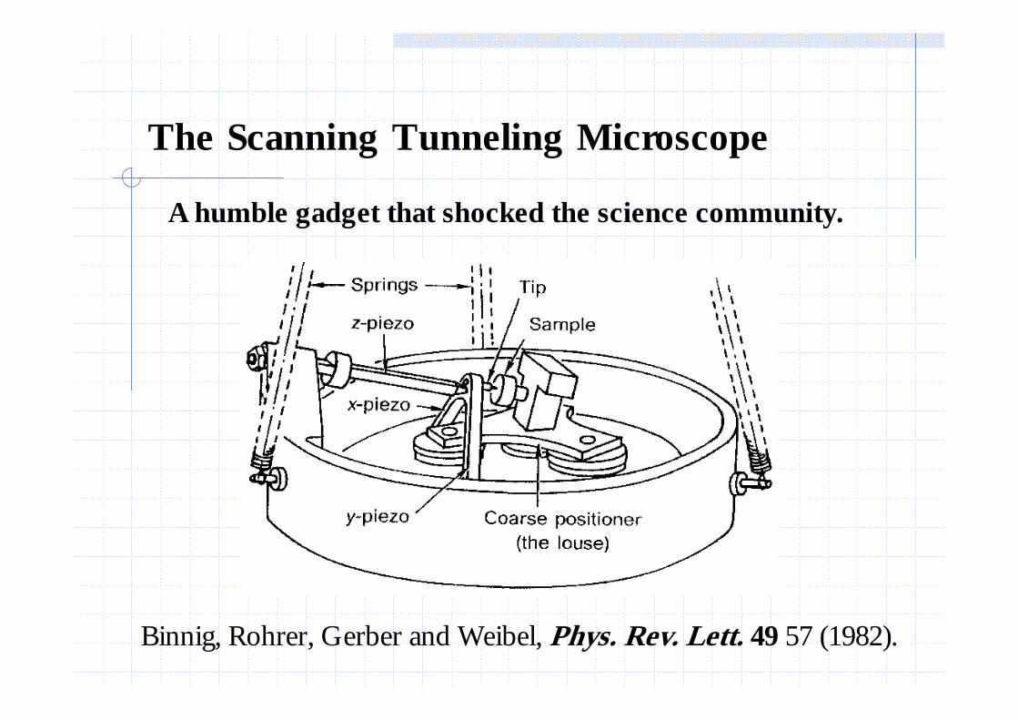
The Scanning Tunneling Microscope
A humble gadget that shocked the science community.
Binnig, Rohrer, Gerber and Weibel, Phys. Rev. Lett. 49 57 (1982).

Nobel Prize in Physics 1986: Binnig and Rohrer

Stairway to Heaven to Touch Atoms
Wiesendanger et al., Phys. Rev. Lett. 65, 247 (1990).

Atomic Resolution on Metal Surfaces
Using STM, individual atoms are routinely resolved on all metal surfaces, with typical interatomic distance of 2.5-3.5 A (0.25-0.35 nm).
Figure: An STM imageof Au(111) surface, showing both large reconstruction and small atomic details.
Barth et al., Phys. Rev. B 42, 9307 (1990).

The Art of STM tip sharpening
(2) By treat the tip with a controlled collision,(3) or, treat the tip with an electrical pulse, atomic resolution may suddenly show up. (4) Often, spontaneous tip restructuring could change the resolution dramatically (for good or for bad).
(1) Even with a carefully made tip, atom resolution would not occur immediately.
? ? ?

Tip-State Dependence of STM Images
Several images of thesame sample takenwithin 2 hours underidentical conditions,showing dramaticdifferences due tochanges in tip states.
R. V. Coleman et al.,Adv. Phys. 37, p.607,(1988).

Spontaneous Corrugation Reversal
After a spontaneous tip restructuring, under identicaltunneling conditions, atomic corrugation reversed.
Barth, Burne, Ertl and Behm, Phys Rev B 42, 9307 (1990).
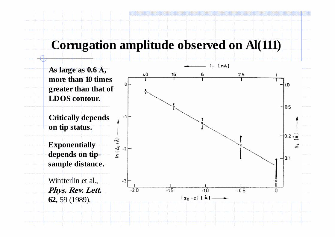
Corrugation amplitude observed on Al(111)
As large as 0.6 Å, more than 10 times greater than that of LDOS contour.
Critically depends on tip status.
Exponentially depends on tip-sample distance.
Wintterlin et al.,Phys. Rev. Lett.62, 59 (1989).

Non-Contact Atomic Force Microscopy (NC-AFM)
Using frequency-modulation method to detect weak attractive atomic force thus to obtain atomic images.
Noncontact Atomic Force Microscopy, Eds. Morita, Wiesendanger, and Meyer, Springer 2002, page 3.
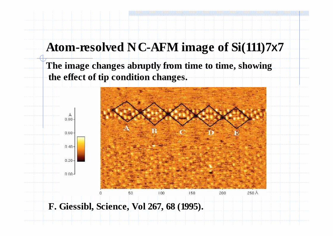
Atom-resolved NC-AFM image of Si(111)7X7
The image changes abruptly from time to time, showing the effect of tip condition changes.
F. Giessibl, Science, Vol 267, 68 (1995).

Tip states: First-principle computations
By modeling the tip as W clusters, Ohnishi and Tsukada found that the tip states near Fermi level are dominated by d-type wavefunctions.
Ohnishi and Tsukada, Solid State Commun. 71, 391 (1989).

Effect of atomic-scale tip electronic states
Conceptually, the effect of tip states can be understood in light ofthe reciprocity principle : At microscopic scale, an image may be interpreted either as probing the sample state with a tip state, or as probing the tip state with a sample state.

Tunneling matrix elements: the derivative rule
The tunneling matrix elements, needed to compute tunneling current,follow a very simple derivative rule:

Quantitative analysis of Al(111) STM images
By assuming a dz2 atomic state on a W tip, the experimental data ofcorrugation vs. distance is recovered with no adjustable parameters.
The dz2 tip state enhances the corrugation amplitude by a factor of 20 over LDOS corrugation.
Exponential dependence of corrugation amplitude on tip-sample distance fully explained.

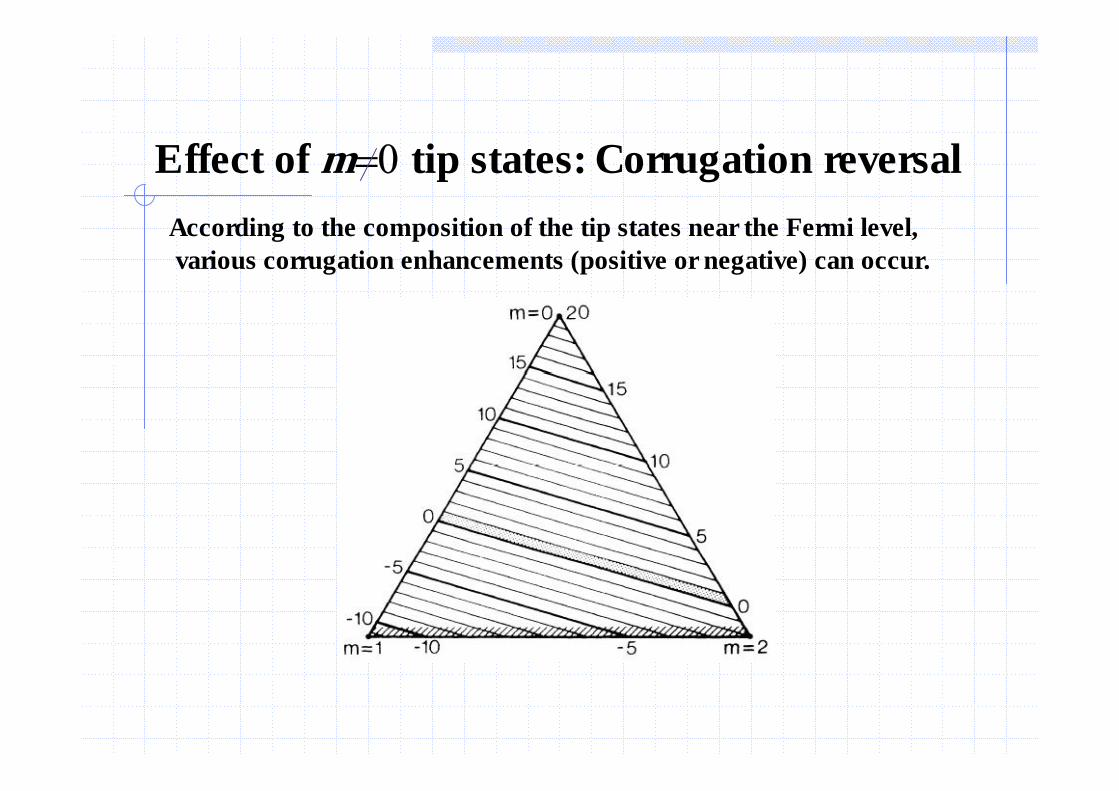
Effect of m=0 tip states: Corrugation reversal
Near the Fermi level, if one of the d-states dominates, the image can be positive or reversed.
s-state
s-state
d-state, m=0
d-state, m=1 d-state, m=2

Effect of m=0 tip states: Corrugation reversal
Mathematically, the phenomena of corrugation reversal can be described by hexagonal cosine functions,
Effect of m=0 tip states: Corrugation reversal
According to the composition of the tip states near the Fermi level, various corrugation enhancements (positive or negative) can occur.

Theoretical and experimental verifications
First-principle computation of tip electronic states.
First-principle computation of surfaces electronic structures and STM images with regard to tip states.
Experimental verifications of the theoretical STM images computed with different tip electronic states.
Experimental observations of tip electronic states by NC-AFM and STM.

First-Principle Computation of STM Tip Electronic States (1)

First-Principle Computation of STM Tip Electronic States (1)
DOS of a W(100) tip:
Peak A comes mainly from dz2 and d x2-y2 states,….. dz2
----- dx2-y2
Peak B comes mainly fromdxy orbital-.-.- dxy
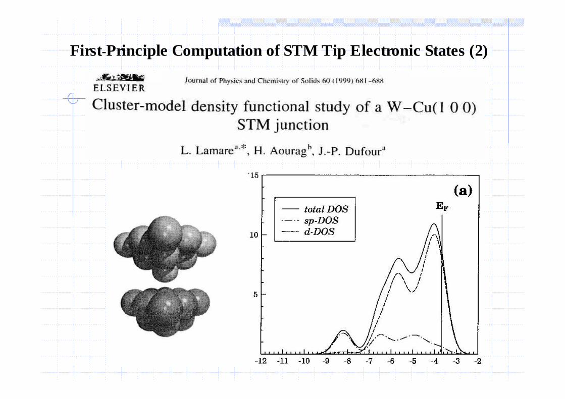
First-Principle Computation of STM Tip Electronic States (2)

First-Principle Computation of STM Tip Electronic States (2)

First-Principle Computation of STM Tip Electronic States (3)

First-Principle Computation of STM Tip Electronic States (3)

First-Principle Computation of STM Tip Electronic States (4)

First-Principle Computation of STM Tip Electronic States (4)

Non-perturbative Theory of STM Images wrt Tip States

Non-perturbative Theory of STM Images wrt Tip States

First-Principle Computation of STM Images wrt Tip States (1)

First-Principle Computation of STM Images wrt Tip States (1)

First-Principle Computation of STM Images wrt Tip States (2)

First-Principle Computation of STM Images wrt Tip States (2)

First-Principle Computation of STM Images wrt Tip States (2)
Tip-state enhancement according to first-Principle computation
Tip-state enhancement according to analytical formulae.

Tip Electronic States Imaged by STM (1)
Using a vibrating STM tip to prevent tip crashing, STM can image tip electronic states in great details.
Herz, Giessibl, and Mannhart, Phys. Rev. B 68, 045301 (2003).

Tip Electronic States Imaged by STM (2)
Herz, Giessibl, and Mannhart, Phys. Rev. B 68, 045301 (2003).
Using Si(111)7X7 as sample, Co6Fe3Sm as tip, a 4f orbitalof an Sm atom is resolved in real space.

Case of spin-polarized STM
-- Well-understood systems with surface magnetism -- Reproducible SP-STM tip production procedures
-- Nearly atomic resolution
SP-STM has achieved great progress recently:
Some ideas about atom-resolved SP-STM-- Mathematical formulation of tip states with spin-- Using the popular tip sharpening procedures-- Experimental tip-state characterization:
> determine z-component of spin polarization> determine azimuth of spin polarization> determine orbital symmetry and type

Single-atom SP-STM tip
3d transition-metal atoms adsorbed on noble or refractive metal tips often show large local magnetic moments.
Stepanyuk et al., Phys Rev B 53 2121 (1996).
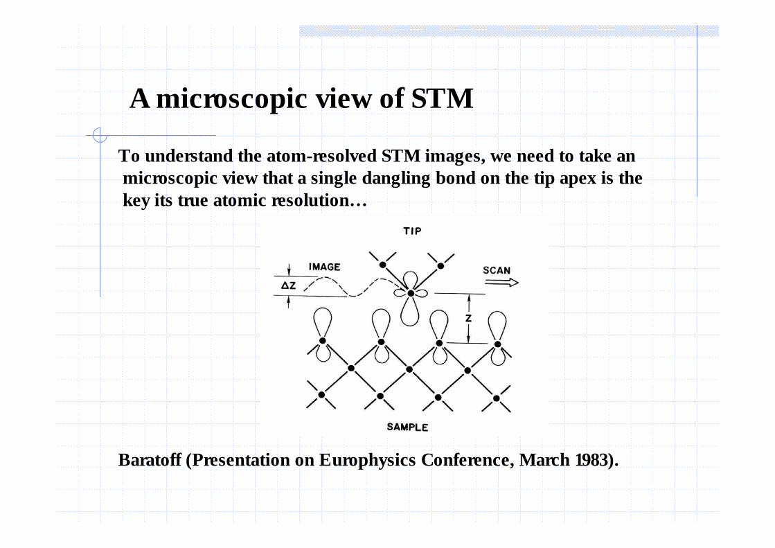
A microscopic view of STM
To understand the atom-resolved STM images, we need to take anmicroscopic view that a single dangling bond on the tip apex is the key its true atomic resolution…
Baratoff (Presentation on Europhysics Conference, March 1983).

Electronic states of W tip with Cr or Mn adsorbed
Electronic states ofSTM tip: Cr or Mnatom adsorbed onW tip.
3d states dominatetip DOS.
At 0.1 to 0.4 eV below Fermi level, Mn tipstate (3dz2) is highly spin-polarized.
Hofer, Redinger and Podlousky, PRB 64 125108 (2001).

Electronic states of W tip with Cr or Mn adsorbed
For both Crand Mn, themajority tipstate is dZ2
type.
Therefore, itis possibleto get spin-polarized informationand atomicresolution.
Hofer, Redinger and Podlousky, PRB 64 125108 (2001).

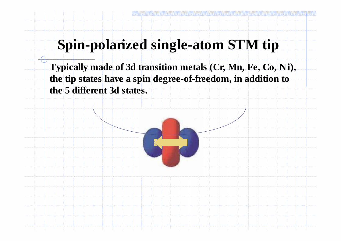
Spin-polarized single-atom STM tip
Typically made of 3d transition metals (Cr, Mn, Fe, Co, Ni), the tip states have a spin degree-of-freedom, in addition to the 5 different 3d states.
Spin-polarized single-atom STM tip
Typically made of 3d transition metals (Cr, Mn, Fe, Co, Ni), the tip states have a spin degree-of-freedom, in addition to the 5 different 3d states.

Spin-polarized single-atom STM tip
Typically a 3d atom (Cr, Mn, Fe, Co, Ni). The d-shell has 5 different orbital wavefunctions. Each of those has two spin-polarizations.Each of the 10 states has its energy level and
spectral broadenings.Some are filled states, some are empty states.If different spin-polarized state has different
energy levels, a net spin polarization exists.With a well-characterized sample, the tip states
can be determined experimentally.
Spin-polarized single-atom STM tip
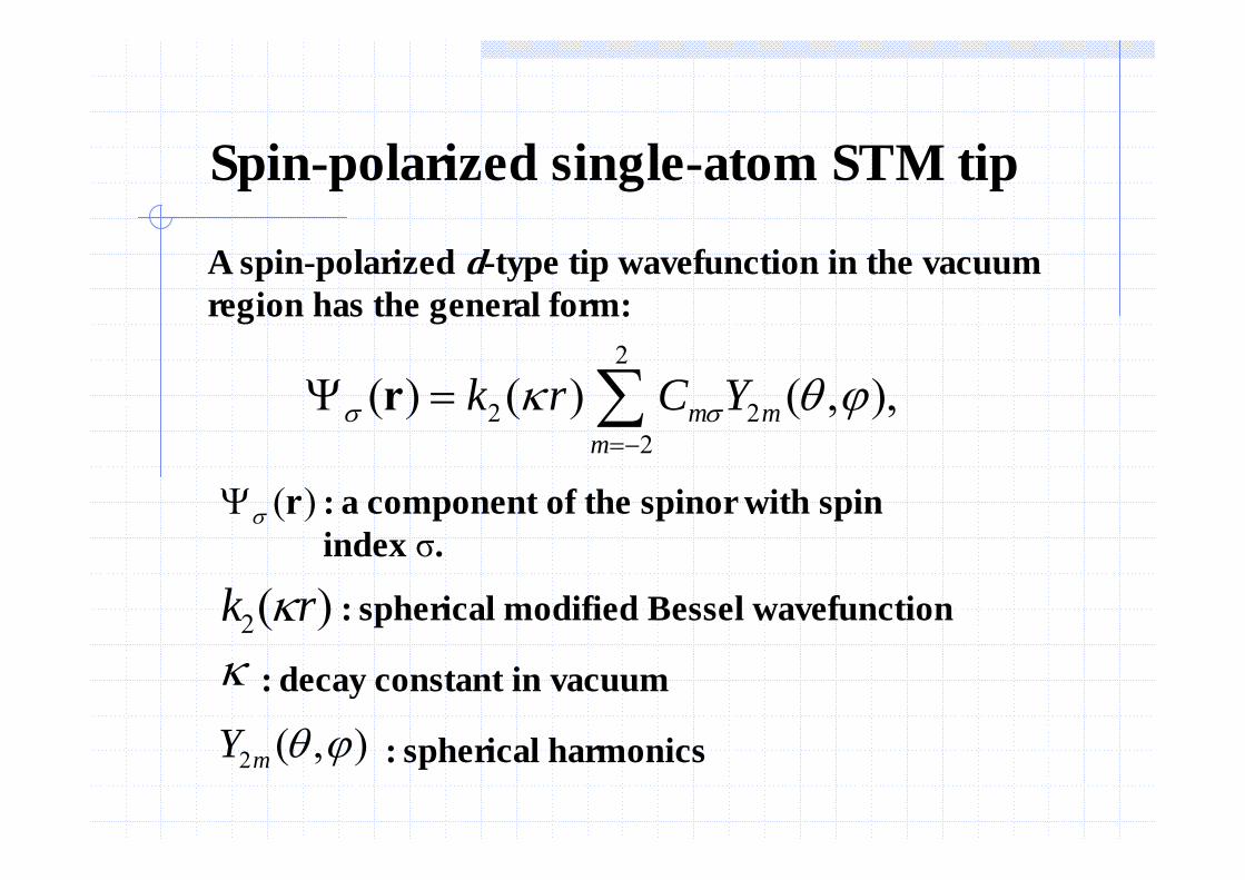
A spin-polarized d-type tip wavefunction in the vacuum region has the general form:
2
2 22
( ) ( ) ( , ),m mm
k r C Yσ σκ θ ϕ=−
Ψ = ∑r
( )σΨ r : a component of the spinor with spin index σ.
2( )k rκ : spherical modified Bessel wavefunction
2 ( , )mY θ ϕ : spherical harmonics
κ : decay constant in vacuum

Generating spin-polarized tip using controlled collision and electrical pulses
(3) By treat the tip with a controlled collision,(4) or, treat the tip with an electrical pulse, a variety of magnetic contrasts can be generated.
(2) Using a non-magnetic tip, for example W.(1) Start with a magnetic material, Cr, Mn, Fe, Gd, etc.
Yamada, Bishoff, Mizoguchi and van Kempen, Appl. Phys. Lett.82 1437 (2003).

Generating spin-polarized tip using controlled collision and electrical pulses
Yamada, Bishoff, Mizoguchi and van Kempen, Appl. Phys. Lett.82 1437 (2003).

SP-STM with tip characterization
Tip-treatmentstage: Cr, Mn, …
Tip-characterization stage: Fe/W(110), Si(111)7X7
Target-sample imaging stage
(2). Treat the tip with a controlled collision.(3). Or, treat the tip with an electrical pulse.
(1). Bring the tip to the tip-treatment stage.

SP-STM with tip characterization
Tip-treatmentstage: Cr, Mn, …
Tip-characterization stage: Fe/W(110), Si(111)7X7
Target-sample imaging stage
(4). Characterize the tip with a standard surface.

SP-STM with tip characterization
Tip-treatmentstage: Cr, Mn, …
Tip-characterization stage: Fe/W(110), Si(111)7X7
Target-sample imaging stage
(5). Using the characterized tip to probe a sample.

SP-STM tip characterization
Using Fe/W(110) to determine spin polarization of tip states, with a rotating-tip STM.
Pietzsch, Kubetzka, Bode, and Wiesendanger, Phys. Rev. Lett.84 5212 (2000).

SP-STM tip characterization
Using Fe/W(110) to determine spin polarization of tip states, with a rotating-tip STM.
Pietzsch, Kubetzka, Bode, and Wiesendanger, Phys. Rev. Lett.84 5212 (2000).

SP-STM tip characterization
Using Fe/W(110) to determine spin polarization of tip states, with a rotating-tip STM.
Pietzsch, Kubetzka, Bode, and Wiesendanger, Phys. Rev. Lett.84 5212 (2000).

SP-STM tip characterization
Using Fe/W(110) to determine spin polarization of tip states, with a rotating-tip STM.
Pietzsch, Kubetzka, Bode, and Wiesendanger, Phys. Rev. Lett.84 5212 (2000).

SP-STM tip characterization
Using Fe/W(110) to determine spin polarization of tip states, with a rotating-tip STM.
Pietzsch, Kubetzka, Bode, and Wiesendanger, Phys. Rev. Lett.84 5212 (2000).

SP-STM tip characterization
Using Fe/W(110) to determine spin polarization of tip states, with a rotating-tip STM.
Pietzsch, Kubetzka, Bode, and Wiesendanger, Phys. Rev. Lett.84 5212 (2000).

The Si(111)7X7 Surface Structure
The distance between adjacent adatoms is 7 Å. Its electronic structure is well-understood. Therefore, it is ideal for tip-state determination.

Tip Electronic States Imaged by NC-AFM
Franz J. Giessibl et al., Science,Science, Vol. 289, p 422 – p 425, July 21, 2000.
Each image of an adatom on Si(111)7X7 is split into two.
The topography of each groupis very similar.
The only possible interpretation:Each group is an image of the tipelectronic states, probed by anadatom on Si(111)7X7 sample.
A manifestation of reciprocityreciprocityprincipleprinciple in STM imaging.
An example of inversed STM:inversed STM:imaging the tip with a “sample”.

Spin-polarized NC-AFM
Studying magnetism in insulators -- Tunneling experiment cannot be conducted. NC-AFM works.
Force measurement complements tunneling-- Valuable also for magnetic properties of conductors.
Direct measurement of exchange interactions-- visualize the origin of Heisenberg’s exchange coupling.
Related issues: -- A universal relation between tunneling conductance, chemical
bond, and exchange coupling as the origin of magnetism.
-- Basic physics of atom manipulation (pulling and sliding).

Heisenberg Hamiltonian (1928)
2 .eff ij i ji j
JH>
= − ∑ S S
Spin vector of the i th atom
Spin vector of the j th atom
Coefficients depending on the displacement between the i th atom and the j th atom.-- decaying with distance (a few atoms away)-- orientation dependent (magnetic anisotropy)
iS
jS
ijJ

Origin of exchange coupling coefficients Jij
The initial idea of exchange coupling came from Heitlerand London’s treatment of hydrogen molecule (1927).
C. Herring, Direct Exchange between Well-Separated Atoms, in Magnetism, Vol. IIB, Eds. Rado and Suhl, 1966.
However, the Heitler -London treatment diverges at large distances, and does not give the correct initial states.
An asymptotically correct treatment (Holstein, Landau, and Herring) is based on first-order perturbation theory.
An extension to time-dependent perturbation theory provides a unified view of tunneling, chemical bond, and exchange coupling in magnetism.

A related issue: Relation between STM and NC-AFM
What is the physical origin of atomic resolution in STM and NC-AFM?
What kind of scientific knowledge can we extract from the atom-resolved STM and NC-AFM images, and how?
What is the relation between tunneling conductance and attractive atomic force in STM and NC-AFM?
What can we do to improve the experimental conditionsof STM and NC-AFM to enlarge the information channelto Mother Nature?

Covalent bond and tunneling matrix element
After C. Herring, Critique of the Heitler-London method of calculating spin couplings at large distances, Rev. Mod. Phys., 34, 631-645 (1962).
The problem of H2+
Large distances: r > 6 Avan del Waals force
Intermediate distances: 2-6 A tunneling, covalent bond, and exchange coupling.
Very short distances: r < 2 A core-core repulsion
o
o
o

Covalent bond and tunneling matrix element
The problem of H2+
After C. Herring, Critique of the Heitler-London method of calculating spin couplings at large distances, Rev. Mod. Phys., 34, 631-645 (1962).
By correctly choosing the unperturbed potential for the hydrogen atoms, using first-order perturbation theory, the exchange coupling energy (or the covalent bonding energy) can be accurately evaluated.

Covalent bond and tunneling matrix element
The Bardeen tunneling matrix element can be evaluated analytically for the case of hydrogen molecule ion.
Covalent bond energy in H2+: exact solution vs. tunneling evaluation.
[ ]122 .
R L L R
R
M d
Ree
ψ ψ ψ ψ
−
= ∇ − ∇
= −
∫ S

Covalent bond and tunneling matrix element
Tunneling evaluation of H2+ energy levels
4
9 2(1 ) ,4
RgE Re
R eσ −∆ = − −
4
9 2(1 ) .4
RuE Re
R eσ −∆ = − +
Exact solution of H2+
4 6 7
2
9 15 2134 2 42 1 251 ....
2 8R
ER R R
Ree R R
±
−
∆ = − − −
⎛ ⎞± + − +⎜ ⎟⎝ ⎠
Van del Waals
Exchange interaction

Covalent bond and tunneling matrix element
The Bardeen tunneling matrix element almost exactly equals the chemical bonding energy and the exchange coupling energy.
Covalent bond energy in H2+: exact solution vs. tunneling evaluation.
Bonding energyin eV.
Proton-proton distance in A
Solid curve: exact solution
Crosses: tunneling matrix element
o

Relation between bonding energy and tunneling
The bonding energy between the tip atom and an atom on the sample is determined by the overlap of the two wavefunctions,
( ),E E= RR
R
where is the vector distance betweenthe nuclei of the two atoms.
The tunneling matrix element between the two atoms is also determined by the overlap of the two wavefunctions, thus
( ).M M= RIntuitively, there should be a relation between the two quantities.

A universal relation between attractive atomic force and tunneling conductance
Using Fermi golden rule, tunneling conductance is
| | .MFz
∂= −
∂
2/KR h e=
( )2 22| | .S T
K
G MRπ
ρ ρ=
Tρ
Attractive atomic force (chemical bond force) is
≈ 25.812 kΩ: von Klitzing’s constant
: sample DOS at Fermi level
: tip DOS at Fermi level
Sρ

An experimentally verifiable relation
: tip geometry form factor
22 ,K
S T
f RF Gκρ ρ
=
KRSρTρ1f ≈
Using time-dependent perturbation theory, a universal relation between tunneling conductance G = dI/dUand attractive atomic force F is derived,
≈ 25.812 kΩ: von Klitzing’s constant
: sample DOS at Fermi level
: tip DOS at Fermi level
Chen, J. Phys. Cond. Matter, Vol 3, 1227 (1991); Introduction to Scanning Tunneling Microscopy, 1993, Chapter 7.

Experimental verification of F 2~G relation (1)

Experimental verification of F 2~G relation (1)

Experimental verification of F 2~G relation (2)

Experimental verification of F 2~G relation (2)

Suggested experiments
Simultaneous measurement of attractive atomic force and tunneling conductance
- Verify the equivalence of tunneling and chemical bond.
- Extract tip and sample electronic information
Conduct spin-polarized NC-AFM experiments
- Main difficulty: tip formation and tip characterization
- Tip formation by controlled collision and electrical pulse
- Using SP-STM to characterize SP-AFM tip

Experimental verification of F 2~G relation

Example of a recent measurement of I-Z relation
Hla, Braun and Rieder, PRB 67 201402 R (2003).
W tip on Ag(111) sample, ~6K.

Spin-polarized NC-AFM: possible contrast mechanisms
Tip with in-plane spin polarization, rotating tip.
Tip with perpendicular (out-of-plane) spin polarization, exchange tip (or recondition tip).
Tip with in-plane spin polarization, atoms on sample surface has different in-plane spin polarizations.
Tip with out-of-plane spin polarization, atoms on sample surface has different out-of-plane spin polarizations.
Bias-dependent non-contact force effects.

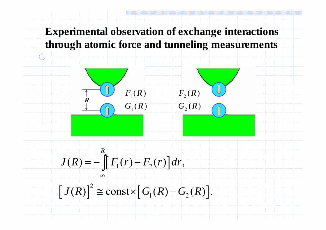
Experimental observation of exchange interactions through atomic force and tunneling measurements
R 1
1
( )( )
F RG R
2
2
( )( )
F RG R
[ ]
[ ] [ ]
1 2
21 2
( ) ( ) ( ) ,
( ) const ( ) ( ) .
R
J R F r F r dr
J R G R G R∞
= − −
≅ × −
∫
Experimental observation of exchange interactions through atomic force and tunneling measurements
R 1
1
( )( )
F RG R
2
2
( )( )
F RG R
[ ]
[ ] [ ]
1 2
21 2
( ) ( ) ( ) ,
( ) const ( ) ( ) .
R
J R F r F r dr
J R G R G R∞
= − −
≅ × −
∫

Experimental problem: Tip characterization
Tip preparation and tip characterization can be follow the same method as in tunneling experiments.
With a tip rotation mechanism, the azimuth of spin polarization can be controlled.
Because tunneling (including STS) can provide complete information about tip states, but with greater ease and greater richness than AFM, the tip can be characterized with tunneling experiments.

Another related issue:Physical mechanism of atom manipulation
What is the force that moves the atoms?
What is the relation between that force and tunneling?
How to control atom moving precisely?

The Art of Atom Manipulation
Controlled manually.
Each move takes days.
It takes weeks to makean “IBM” pattern.
It made headline news.
No reproducible recipeever published.

Atom manipulation: Towards an exact science (1)
Basic steps of atommanipulation
pulling
sliding
Bartels, Meyer and Rieder,PRL 79 697 (1997).
Meyer, Moresco, Hla, Repp, Foelsch and Rieder, JJAP 40 4409 (2001).
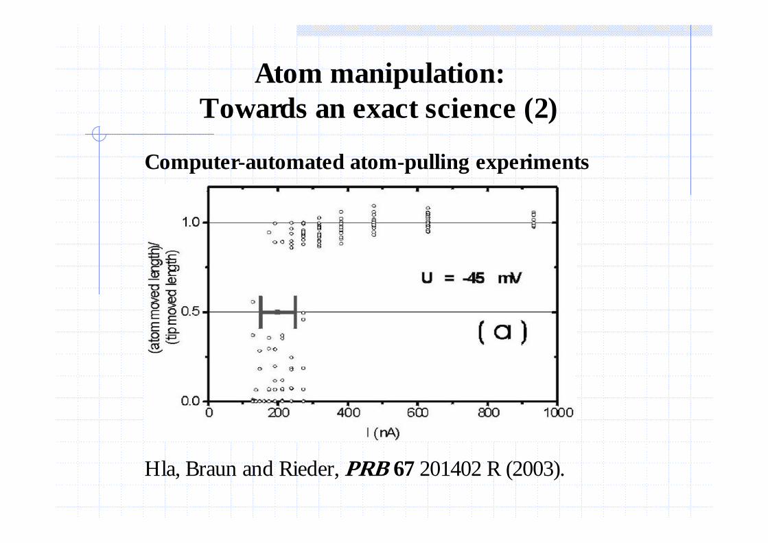
Atom manipulation: Towards an exact science (2)
Computer-automated atom-pulling experiments
Hla, Braun and Rieder, PRB 67 201402 R (2003).

Atom manipulation: Towards an exact science (3)
Hla, Braun and Rieder, PRB 67 201402 R (2003).
A well-defined threshold tunneling resistance is found.

Atom manipulation: Towards an exact science (4)
Hla, Braun and Rieder, PRB 67 201402 R (2003).
Complicated patterns can be generated by programming.

Atom manipulation: Towards an exact science (4)
What is the meaning of threshold tunneling resistance?
The force is independent of the magnitude of bias.
The force is independent of the polarity of bias.
Therefore, it is not related to electrical field or current.
It is the formation of a partial chemical bond.
If this is true, then the threshold tunneling resistanceshould be directly related to the diffusion barrierheight for the atom to move over. And this can be verified experimentally.

Atom manipulation: A proposed new experiment

SummaryAtomic resolution in STM and NC-AFM- The art of tip sharpening
- The mystery of spontaneous tip restructuring
Understand and characterize tip states - Existence and manifestation of various tip states
- Experimental determination of various tip states
- Case of spin-polarized STM
Spin-polarized non-contact AFM - A unified view of tunneling, chemical bond, and magnetism
- Probe chemical bonds through tunneling measurements
- Probe exchange coupling by force and tunneling measurements
- Atom manipulation: from personal art to exact science