stm32l432kb/kc stm32l442kc applicability...spi 2.15.1 bsy bit may stay high at the end of data...
TRANSCRIPT

ApplicabilityThis document applies to the part numbers of STM32L432KB/KC and STM32L442KC devices and the device variants as statedin this page.
It gives a summary and a description of the device errata, with respect to the device datasheet and reference manual RM394.
Deviation of the real device behavior from the intended device behavior is considered to be a device limitation. Deviation of thedescription in the reference manual or the datasheet from the intended device behavior is considered to be a documentationerratum. The term “errata” applies both to limitations and documentation errata.
Table 1. Device variants
ReferenceSilicon revision codes
Device marking(1) REV_ID(2)
STM32L432KB/KC, STM32L442KCA 0x1000
Z 0x1001
1. Refer to the device data sheet for how to identify this code on different types of package.2. REV_ID[15:0] bitfield of DBGMCU_IDCODE register.
STM32L432KB/KC and STM32L442KC device errata
STM32L432KB/KC STM32L442KC
Errata sheet
ES0319 - Rev 5 - July 2019For further information contact your local STMicroelectronics sales office.
www.st.com
1 Summary of device errata
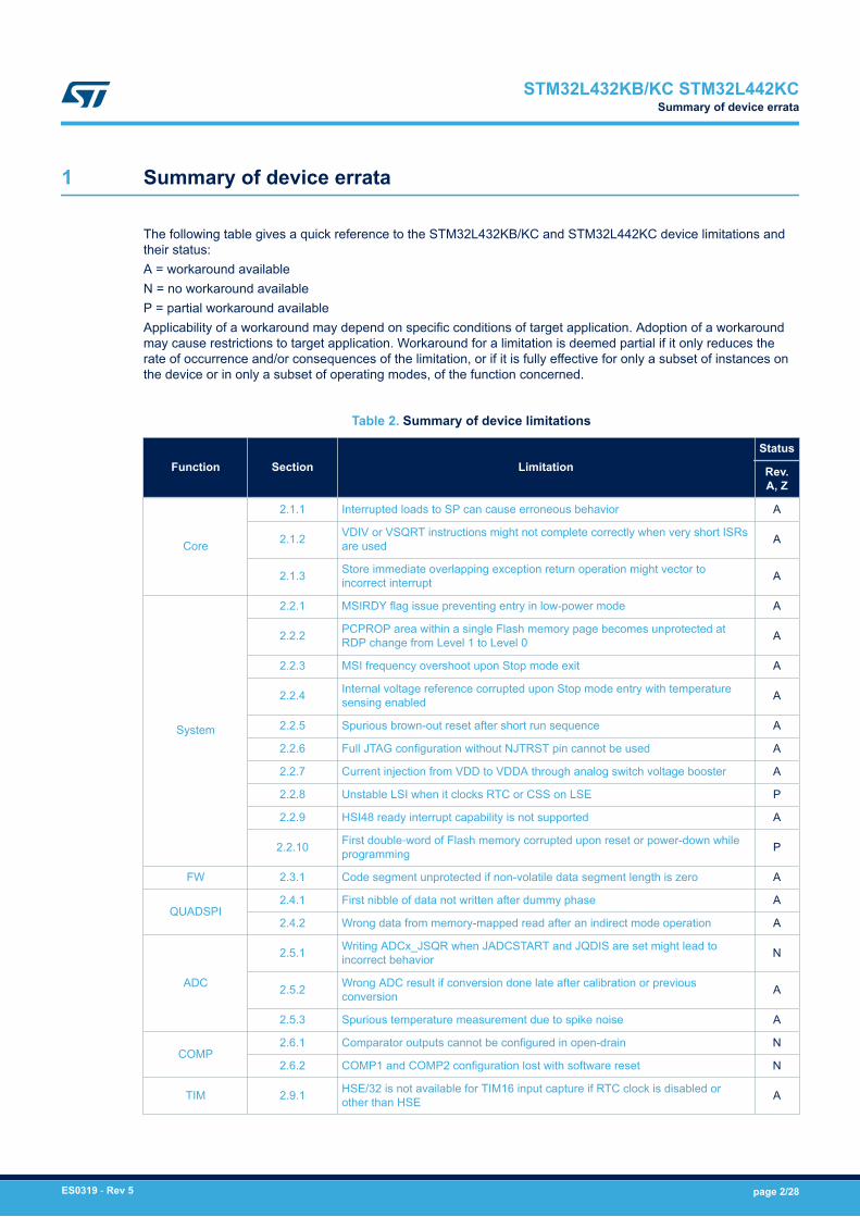
The following table gives a quick reference to the STM32L432KB/KC and STM32L442KC device limitations andtheir status:A = workaround availableN = no workaround availableP = partial workaround availableApplicability of a workaround may depend on specific conditions of target application. Adoption of a workaroundmay cause restrictions to target application. Workaround for a limitation is deemed partial if it only reduces therate of occurrence and/or consequences of the limitation, or if it is fully effective for only a subset of instances onthe device or in only a subset of operating modes, of the function concerned.
Table 2. Summary of device limitations
Function Section LimitationStatus
Rev.A, Z
Core
2.1.1 Interrupted loads to SP can cause erroneous behavior A
2.1.2 VDIV or VSQRT instructions might not complete correctly when very short ISRsare used A
2.1.3 Store immediate overlapping exception return operation might vector toincorrect interrupt A
System
2.2.1 MSIRDY flag issue preventing entry in low-power mode A
2.2.2 PCPROP area within a single Flash memory page becomes unprotected atRDP change from Level 1 to Level 0 A
2.2.3 MSI frequency overshoot upon Stop mode exit A
2.2.4 Internal voltage reference corrupted upon Stop mode entry with temperaturesensing enabled A
2.2.5 Spurious brown-out reset after short run sequence A
2.2.6 Full JTAG configuration without NJTRST pin cannot be used A
2.2.7 Current injection from VDD to VDDA through analog switch voltage booster A
2.2.8 Unstable LSI when it clocks RTC or CSS on LSE P
2.2.9 HSI48 ready interrupt capability is not supported A
2.2.10 First double‑word of Flash memory corrupted upon reset or power-down whileprogramming P
FW 2.3.1 Code segment unprotected if non-volatile data segment length is zero A
QUADSPI2.4.1 First nibble of data not written after dummy phase A
2.4.2 Wrong data from memory-mapped read after an indirect mode operation A
ADC
2.5.1 Writing ADCx_JSQR when JADCSTART and JQDIS are set might lead toincorrect behavior N
2.5.2 Wrong ADC result if conversion done late after calibration or previousconversion A
2.5.3 Spurious temperature measurement due to spike noise A
COMP2.6.1 Comparator outputs cannot be configured in open-drain N
2.6.2 COMP1 and COMP2 configuration lost with software reset N
TIM 2.9.1 HSE/32 is not available for TIM16 input capture if RTC clock is disabled orother than HSE A
STM32L432KB/KC STM32L442KCSummary of device errata
ES0319 - Rev 5 page 2/28

Function Section LimitationStatus
Rev.A, Z
LPTIM
2.10.1 MCU may remain stuck in LPTIM interrupt when entering Stop mode A
2.10.2 MCU may remain stuck in LPTIM interrupt when clearing event flag P
2.10.3 LPTIM1 outputs cannot be configured as open‑drain N
RTC and TAMP
2.11.1 RTC calendar registers are not locked properly A
2.11.2 RTC interrupt can be masked by another RTC interrupt A
2.11.3 Calendar initialization may fail in case of consecutive INIT mode entry A
2.11.4 RTC_REFIN and RTC_OUT on PB2 not operating in Stop 2 mode P
I2C
2.12.1 10-bit master mode: new transfer cannot be launched if first part of the addressis not acknowledged by the slave A
2.12.3 Wrong data sampling when data setup time (tSU;DAT) is shorter than one I2Ckernel clock period P
2.12.4 Spurious bus error detection in master mode A
2.12.5 Last-received byte loss in reload mode P
2.12.6 Spurious master transfer upon own slave address match P
USART 2.13.1 RTS is active while RE = 0 or UE = 0 A
LPUART 2.14.1 LPUART1 outputs cannot be configured as open‑drain N
SPI
2.15.1 BSY bit may stay high at the end of data transfer in slave mode A
2.15.2 Wrong CRC in full-duplex mode handled by DMA with imbalanced setting ofdata counters A
2.15.4 SPI master communication failure at high fPCLK within the specified range N
bxCAN 2.16.1 bxCAN time-triggered communication mode not supported A
The following table gives a quick reference to the documentation errata.
Table 3. Summary of device documentation errata
Function Section Documentation erratum
TSC 2.7.1 Inhibited acquisition in short transfer phase configuration
AES(1)
2.8.1 Burst read or write accesses not supported
2.8.2 TAG computation in GCM encryption mode
2.8.3 CCM authentication mode not compliant with NIST CMAC
2.8.4 Datatype initial configuration in GCM mode
2.8.5 Wait until BUSY is low when suspending GCM encryption
RTC andTAMP 2.11.5 Setting GPIO properties of PC13 used as RTC_ALARM open-drain output
I2C 2.12.2 Wrong behavior in Stop mode when wakeup from Stop mode is disabled in I2C
SPI 2.15.3 CRC error in SPI slave mode if internal NSS changes before CRC transfer
1. Only applicable to STM32L442KC
STM32L432KB/KC STM32L442KCSummary of device errata
ES0319 - Rev 5 page 3/28

2 Description of device errata
The following sections describe limitations of the applicable devices with Arm® core and provide workarounds ifavailable. They are grouped by device functions.
Note: Arm is a registered trademark of Arm Limited (or its subsidiaries) in the US and/or elsewhere.
2.1 Core
Errata notice for the Arm® Cortex®-M4F core revision r0p1 is available from http://infocenter.arm.com.
2.1.1 Interrupted loads to SP can cause erroneous behaviorThis limitation is registered under Arm ID number 752770 and classified into “Category B”. Its impact to the deviceis minor.
Description
If an interrupt occurs during the data-phase of a single word load to the stack-pointer (SP/R13), erroneousbehavior can occur. In all cases, returning from the interrupt will result in the load instruction being executed anadditional time. For all instructions performing an update to the base register, the base register will be erroneouslyupdated on each execution, resulting in the stack-pointer being loaded from an incorrect memory location.The affected instructions that can result in the load transaction being repeated are:• LDR SP, [Rn],#imm• LDR SP, [Rn,#imm]!• LDR SP, [Rn,#imm]• LDR SP, [Rn]• LDR SP, [Rn,Rm]
The affected instructions that can result in the stack-pointer being loaded from an incorrect memory address are:• LDR SP,[Rn],#imm• LDR SP,[Rn,#imm]!
As compilers do not generate these particular instructions, the limitation is only likely to occur with hand-writtenassembly code.
Workaround
Both issues may be worked around by replacing the direct load to the stack-pointer, with an intermediate load to ageneral-purpose register followed by a move to the stack-pointer.
2.1.2 VDIV or VSQRT instructions might not complete correctly when very short ISRs are usedThis limitation is registered under Arm ID number 776924 and classified into “Category B”. Its impact to the deviceis limited.
Description
The VDIV and VSQRT instructions take 14 cycles to execute. When an interrupt is taken a VDIV or VSQRTinstruction is not terminated, and completes its execution while the interrupt stacking occurs. If lazy context saveof floating point state is enabled then the automatic stacking of the floating point context does not occur until afloating point instruction is executed inside the interrupt service routine.Lazy context save is enabled by default. When it is enabled, the minimum time for the first instruction in theinterrupt service routine to start executing is 12 cycles. In certain timing conditions, and if there is only one or twoinstructions inside the interrupt service routine, then the VDIV or VSQRT instruction might not write its result to theregister bank or to the FPSCR.The failure occurs when the following condition is met:1. The floating point unit is enabled
STM32L432KB/KC STM32L442KCDescription of device errata
ES0319 - Rev 5 page 4/28

2. Lazy context saving is not disabled3. A VDIV or VSQRT is executed4. The destination register for the VDIV or VSQRT is one of s0 - s155. An interrupt occurs and is taken6. The interrupt service routine being executed does not contain a floating point instruction7. Within 14 cycles after the VDIV or VSQRT is executed, an interrupt return is executedA minimum of 12 of these 14 cycles are utilized for the context state stacking, which leaves 2 cycles forinstructions inside the interrupt service routine, or 2 wait states applied to the entire stacking sequence (whichmeans that it is not a constant wait state for every access).In general, this means that if the memory system inserts wait states for stack transactions (that is, externalmemory is used for stack data), then this erratum cannot be observed.The effect of this erratum is that the VDIV or VQSRT instruction does not complete correctly and the register bankand FPSCR are not updated, which means that these registers hold incorrect, out of date, data.
Workaround
A workaround is only required if the floating point unit is enabled. A workaround is not required if the stack is inexternal memory.There are two possible workarounds:• Disable lazy context save of floating point state by clearing LSPEN to 0 (bit 30 of the FPCCR at address
0xE000EF34).• Ensure that every interrupt service routine contains more than 2 instructions in addition to the exception
return instruction.
2.1.3 Store immediate overlapping exception return operation might vector to incorrect interruptThis limitation is registered under Arm ID number 838869 and classified into “Category B (rare)”. Its impact to thedevice is minor.
Description
The core includes a write buffer that permits execution to continue while a store is waiting on the bus. Underspecific timing conditions, during an exception return while this buffer is still in use by a store instruction, a latechange in selection of the next interrupt to be taken might result in there being a mismatch between the interruptacknowledged by the interrupt controller and the vector fetched by the processor.The failure occurs when the following condition is met:1. The handler for interrupt A is being executed.2. Interrupt B, of the same or lower priority than interrupt A, is pending.3. A store with immediate offset instruction is executed to a bufferable location.
– STR/STRH/STRB <Rt>, [<Rn>,#imm]– STR/STRH/STRB <Rt>, [<Rn>,#imm]!– STR/STRH/STRB <Rt>, [<Rn>],#imm
4. Any number of additional data-processing instructions can be executed.5. A BX instruction is executed that causes an exception return.6. The store data has wait states applied to it such that the data is accepted at least two cycles after the BX is
executed.– Minimally, this is two cycles if the store and the BX instruction have no additional instructions between
them.– The number of wait states required to observe this erratum needs to be increased by the number of
cycles between the store and the interrupt service routine exit instruction.7. Before the bus accepts the buffered store data, another interrupt C is asserted which has the same or lower
priority as A, but a greater priority than B.Example:The processor should execute interrupt handler C, and on completion of handler C should execute the handler forB. If the conditions above are met, then this erratum results in the processor erroneously clearing the pendingstate of interrupt C, and then executing the handler for B twice. The first time the handler for B is executed it will
STM32L432KB/KC STM32L442KCCore
ES0319 - Rev 5 page 5/28

be at interrupt C's priority level. If interrupt C is pended by a level-based interrupt which is cleared by C's handlerthen interrupt C will be pended again once the handler for B has completed and the handler for C will beexecuted.As the STM32 interrupt C is level based, it eventually becomes pending again and is subsequently handled.
Workaround
For software not using the memory protection unit, this erratum can be worked around by setting DISDEFWBUFin the Auxiliary Control Register.In all other cases, the erratum can be avoided by ensuring a DSB occurs between the store and the BXinstruction. For exception handlers written in C, this can be achieved by inserting the appropriate set of intrinsicsor inline assembly just before the end of the interrupt function, for example:ARMCC:
...__schedule_barrier();__asm{DSB};__schedule_barrier();}
GCC:
...__asm volatile ("dsb 0xf":::"memory");}
2.2 System
2.2.1 MSIRDY flag issue preventing entry in low-power mode
Description
If the MSI clock is stopped when it is running at high frequency (24 MHz or above), the MSIRDY (MSI ready) flagcan stay at value 1 instead of 0.Once this flag remains set while the MSI clock is off, entry in Stop 0, Stop 1, Stop 2, Standby and Shutdownmodes is no longer possible (the product is blocked in the low-power mode entry phase).The following factors increase the probability to have this issue:• high MSI frequency• low VDD external supply• high temperature
Workaround
• The MSI clock can run at any frequency if both conditions below are met:– The system clock is MSI or PLL fed by MSI when requesting entry in low-power mode.– The wakeup clock is MSI.
• If the system clock is any other clock than MSI, lower the MSI frequency to 16 MHz (or less) and add a shortdelay loop (200 ns minimum) before stopping MSI by software. This ensures that the MSIRDY flag be really0 before requesting entry in low-power mode.
• If the system clock is MSI and the wakeup clock is not MSI, lower the MSI frequency to 16 MHz (or less) andadd a short delay loop (200 ns minimum) before requesting entry in low-power mode.
• If the system clock is PLL fed by MSI and the wakeup clock is not MSI, the MSI frequency used as PLL inputshould not exceed 16 MHz. In other words, do not use the PLL fed by MSI as system clock with MSI at highfrequency (24 MHz or above) divided by PLLM (ensuring the PLL input is between 4 and 16 MHz).
STM32L432KB/KC STM32L442KCSystem
ES0319 - Rev 5 page 6/28

2.2.2 PCPROP area within a single Flash memory page becomes unprotected at RDP change fromLevel 1 to Level 0
Description
With PCROP_RDP option bit cleared, the change of RDP from Level 1 to Level 0 normally results in erasure ofFlash memory banks except the Flash memory pages containing the PCROP area. The PCROP area remainsread-protected.This operates as expected if the PCROP area crosses the limits of at least one Flash memory page, which isalways true if PCROP area size exceeds 2 Kbytes. The limitation occurs if the PCROP area is fully containedwithin one single Flash memory page. Upon the RDP change from Level 1 to Level 0, the Flash memory bankwith PCROP area is not erased and the read protection of the PCROP area is removed.
Workaround
Always define PCROP area such that it crosses limits of at least one Flash memory page.
2.2.3 MSI frequency overshoot upon Stop mode exit
Description
When• the system is clocked by the MSI clock, and• MSI is selected as system clock source upon wakeup from Stop mode, and• a wakeup event occurs only a few system clock cycles before entering Stop mode,
then upon the exit from Stop mode, the MSI frequency can overshoot above its selected range.The limitation applies to all Stop modes: Stop 0, Stop 1, and Stop 2.
Workaround
Apply the following sequence:1. Select HSI16 as system clock.2. Shut MSI down.3. Wait for MSIRDY to go low (after 6 MSI clock cycles).4. Mask interrupts by setting PRIMASK (in the core).5. Initiate Stop mode entry, with MSI selected as system clock source upon wakeup. At this point, the systems
enters Stop mode (unless an early wakeup event occurs). The following steps are done upon Stop modeexit.
6. Enable MSI.7. Wait for MSIRDY to go high.8. Select MSI as system clock.9. Unmask interrupts by clearing PRIMASK.The steps 6 through 8 are required to cover the case of the MCU not entering Stop mode after the step 5 (due toan early wakeup event), thus maintaining HSI16 as system clock.This workaround guarantees the best wakeup time.
2.2.4 Internal voltage reference corrupted upon Stop mode entry with temperature sensing enabled
Description
When entering Stop mode with the temperature sensor channel and the associated ADC(s) enabled, the internalvoltage reference may be corrupted.The occurrence of the corruption depends on the supply voltage and the temperature.The corruption of the internal voltage reference may cause:• an overvoltage in VCORE domain• an overshoot / undershoot of internal clock (LSI, HSI, MSI) frequencies• a spurious brown-out reset
STM32L432KB/KC STM32L442KCSystem
ES0319 - Rev 5 page 7/28

The limitation applies to Stop 1 and Stop 2 modes.
Workaround
Before entering Stop mode:• Disable the ADC(s) using the temperature sensor signal as input, and/or• Disable the temperature sensor channel, by clearing the CH17SEL bit of the ADCx_CCR register.
Disabling both allows consuming less power during Stop mode.
2.2.5 Spurious brown-out reset after short run sequence
Description
When the MCU wakes up from Stop mode and enters the Stop mode again within a short period of time, aspurious brown-out reset may be generated.This limitation depends on the supply voltage (see the following table).
Table 4. Minimum run time
VDD supply voltage (V) Minimum run time (μs)
1.71 15
1.8 13
2.0 11
2.2 9
2.4 8
2.6 6
2.8 5
3.0 3
3.2 and above 2
The minimum run time defined in the previous table corresponds to the firmware execution time on the core.There is no need to add a delay for the wakeup time. Note also that the MCO output length is longer than thefirmware execution time.This limitation applies to Stop 1 and Stop 2 modes.
Workaround
Ensure that the run time between exiting Stop mode and entering Stop mode again is long enough not togenerate a brown-out reset. This can be done by adding a software loop or using a timer to add a delay; thesystem clock frequency can be reduced during this waiting loop in order to minimize power consumption.
2.2.6 Full JTAG configuration without NJTRST pin cannot be used
Description
When using the JTAG debug port in Debug mode, the connection with the debugger is lost if the NJTRST pin(PB4) is used as a GPIO. Only the 4-wire JTAG port configuration is impacted.
Workaround
Use the SWD debug port instead of the full 4-wire JTAG port.
STM32L432KB/KC STM32L442KCSystem
ES0319 - Rev 5 page 8/28

2.2.7 Current injection from VDD to VDDA through analog switch voltage booster
Description
With VDDA below 2.4 V and VDD above 3 V, a small current injected from VDD line to VDDA line may cause VDDAto exceed its nominal value.This current injection only occurs when the I/O analog switch voltage booster is disabled (the BOOSTEN bit of theSYSCFG_CFGR1 register is cleared) and at least one of the analog peripherals (ADC, COMP, DAC, or OPAMP)is enabled.
Workaround
Enable the I/O analog switch voltage booster, by setting the BOOSTEN bit of the SYSCFG_CFGR1 register.when VDDA is below 2.4 V and VDD is above 3 V.
2.2.8 Unstable LSI when it clocks RTC or CSS on LSE
Description
The LSI clock can become unstable (duty cycle different from 50 %) and its maximum frequency can becomesignificantly higher than 32 kHz, when:• LSI clocks the RTC, or it clocks the clock security system (CSS) on LSE (which holds when the LSECSSON
bit set), and• the VDD power domain is reset while the backup domain is not reset, which happens:
– upon exiting Shutdown mode– if VBAT is separate from VDD and VDD goes off then on– if VBAT is tied to VDD (internally in the package for products not featuring the VBAT pin, or externally)
and a short (< 1 ms) VDD drop under VDD(min) occurs
Workaround
Apply one of the following measures:• Clock the RTC with LSE or HSE/32, without using the CSS on LSE• If LSI clocks the RTC or when the LSECSSON bit is set, reset the backup domain upon each VDD power up
(when the BORRSTF flag is set). If VBAT is separate from VDD, also restore the RTC configuration, backupregisters and anti-tampering configuration.
2.2.9 HSI48 ready interrupt capability is not supported
Description
HSI48 ready interrupt feature described in the reference manual is not supported. The bit HSI48RDYIE in theregister RCC_CIER is stuck at 0. It is not possible to set it to interrupt the CPU when the oscillator is ready.
Workaround
After switching the HSI48 internal oscillator on by setting the bit HSI48ON of the RCC_CRRCR register, poll theHSI48RDY flag of the RCC_CRRCR register until it goes high, which indicates that the HSI48 oscillator is readyto provide the clock to peripherals.
2.2.10 First double‑word of Flash memory corrupted upon reset or power-down while programming
Description
Power-down and external reset events occurring during Flash memory program operation may result in zeroing itsfirst double‑word (64 bits on the address 0x0800 0000). When this occurs, the boot sequence ends immediatelyafter reset, generating HardFault.In most cases, this corruption is temporary and the correct value is read again after a few milliseconds. In othercases, it is permanent.
STM32L432KB/KC STM32L442KCSystem
ES0319 - Rev 5 page 9/28

Note: Corruption of Flash memory word on the address accessed in the instant of a reset event occurring duringprogram or erase operation is a normal (specified) behavior.
Workaround
Use one of the following measures:• Clone the first Flash memory page contents at another Flash memory location to use as a backup page. In
the HardFault handler:1. Compare the first Flash memory double‑word content with the value backed up. If different:
a. Erase the first Flash memory page.b. Reprogram HardFault vector.c. From the backup page, restore the first Flash memory page contents, excluding the first
double‑word.d. From the backup page, restore the first Flash memory double‑word.
2. Execute a software reset (by setting the SYSRESETREQ bit), to resume execution.
Caution: If a reset or power-down occurs between the steps 1a and 1b, the MCU never wakes up again.• In the HardFault handler, check whether the HardFault was caused by wrong PC or/and SP loading from the
Flash memory upon reset. If so (the first double-word of the Flash memory is corrupted), jump to the userapplication. Otherwise, perform actions for the system recovery.
Note: In the process of firmware development, the first two 32‑bit words of the Flash memory are used by the core asprogram counter (PC) and as stack pointer (SP), respectively, so this 64‑bit value as well as the remainingcontent of the page can vary upon each build.
2.3 FW
2.3.1 Code segment unprotected if non-volatile data segment length is zero
Description
If during FW configuration the length of firewall-protected non-volatile data segment is set to zero through theLENG[21:8] bitfield of the FW_NVDSL register, the firewall protection of code segment does not operate.
Workaround
Always set the LENG[21:8] bitfield of the FW_NVDSL register to a non-zero value, even if no firewall protection ofdata in the non-volatile data segment is required.
2.4 QUADSPI
2.4.1 First nibble of data not written after dummy phase
Description
The first nibble of data to be written to the external Flash memory is lost when the following condition is met:• QUADSPI is used in indirect write mode.• At least one dummy cycle is used.
Workaround
Use alternate bytes instead of dummy phase to add latency between the address phase and the data phase. Thisworks only if the number of dummy cycles to substitute corresponds to a multiple of eight bits of data.Example:• To substitute one dummy cycle, send one alternate byte (only possible in DDR mode with four data lines).• To substitute two dummy cycles, send one alternate byte in SDR mode with four data lines.
STM32L432KB/KC STM32L442KCFW
ES0319 - Rev 5 page 10/28

• To substitute four dummy cycles, send two alternate bytes in SDR mode with four data lines, or one alternatebyte in SDR mode with two data lines.
• To substitute eight dummy cycles, send one alternate byte in SDR mode with one data line.
2.4.2 Wrong data from memory-mapped read after an indirect mode operation
Description
The first memory-mapped read in indirect mode can yield wrong data if the QUADSPI peripheral enters memory-mapped mode with bits ADDRESS[1:0] of the QUADSPI_AR register both set.
Workaround
Before entering memory-mapped mode, apply the following measure, depending on access mode:• Indirect read mode: clear the QUADSPI_AR register then issue an abort request to stop reading and to clear
the BUSY bit.• Indirect write mode: clear the QUADSPI_AR register.
Caution: The QUADSPI_DR register must not be written after clearing the QUADSPI_AR register.
2.5 ADC
2.5.1 Writing ADCx_JSQR when JADCSTART and JQDIS are set might lead to incorrect behavior
Description
Writing the ADCx_JSQR register when there is an on-going injected conversion (JADCSTART = 1) might lead tounpredictable ADC behavior if the queues of context are not enabled (JQDIS = 1).
Workaround
None.
2.5.2 Wrong ADC result if conversion done late after calibration or previous conversion
Description
The result of an ADC conversion done more than 1 ms later than the previous ADC conversion or ADC calibrationmight be incorrect.
Workaround
Perform two consecutive ADC conversions in single, scan or continuous mode. Reject the result of the firstconversion and only keep the result of the second.
2.5.3 Spurious temperature measurement due to spike noise
Description
Depending on the MCU activity, internal interference may cause temperature‑dependent spike noise on thetemperature sensor output to the ADC, resulting in occasional spurious (outlying) temperature measurement.
Workaround
Perform a series of measurements and process the acquired data samples such as to obtain a mean value notaffected by the outlying samples.For this, it is recommended to use interquartile mean (IQM) algorithm with at least 64 samples. IQM is based onrejecting the quarters (quartiles) of sample population with the lowest and highest values and on computing themean value only using the remaining (interquartile) samples.The acquired sample values are first sorted from lowest to highest, then the sample sequence is truncated byremoving the lowest and highest sample quartiles.
STM32L432KB/KC STM32L442KCADC
ES0319 - Rev 5 page 11/28

Example:
Table 5. Measurement result after IQM post-processing
DataSample
Mean1 2 3 4 5 6 7 8 9 10 11 12
Acquired 17.2 10.92 9.56 2.12 9.82 10.72 10.6 3.5 9.46 9.78 9.5 1.1 8.69
Sorted 1.1 2.12 3.5 9.46 9.5 9.56 9.78 9.82 10.6 10.72 10.92 17.2 8.69
Truncated - - - 9.46 9.5 9.56 9.78 9.82 10.6 - - - 9.79
The measurement result after the IQM post‑processing in the example is 9.79. For consistent results, use aminimum of 64 samples. It is recommended to optimize the code performing the sort task such as to minimize itsprocessing power requirements.
2.6 COMP
2.6.1 Comparator outputs cannot be configured in open-drain
Description
Comparator outputs are always forced in push-pull mode whatever the GPIO output type configuration bit value.
Workaround
None.
2.6.2 COMP1 and COMP2 configuration lost with software reset
Description
The control and status registers of the comparators COMP1 and COMP2 (COMP1_CSR and COMP2_CSR)should be protected against software changes when the LOCK bit is set. Therefore, these registers should bereset only by a system reset. However, it is possible to reset these registers by setting the SYSCFGRST bit of theRCC_APB2RSTR register.
Workaround
None.
2.7 TSC
2.7.1 Inhibited acquisition in short transfer phase configuration
Description
Some revisions of the reference manual may omit the information that the following configurations of the TSC_CRregister are forbidden:• The PGPSC[2:0] bitfield set to 000 and the CTPL[3:0] bitfield to 0000 or 0001• The PGPSC[2:0] bitfield set to 111 and the CTPL[3:0] bitfield to 0000
Failure to respect this restriction leads to an inhibition of the acquisition.This is a documentation inaccuracy issue rather than a product limitation.
Workaround
No application workaround is required.
STM32L432KB/KC STM32L442KCCOMP
ES0319 - Rev 5 page 12/28

2.8 AES
2.8.1 Burst read or write accesses not supported
Description
Some revisions of the reference manual may omit the information that the AES peripheral does not support LDM,STM, LDRD and STRD instructions for successive multiple-data (burst) read and write accesses to a contiguousaddress block.This is a documentation issue rather than a product limitation.
Workaround
No application workaround is required, provided that the multiple-data instructions are not used to access theAES peripheral.
Note: To prevent compilers from generating LDM, STM, LDRD and STRD instructions to access the AES peripheral,organize the source code such as to avoid consecutive read or write accesses to neighboring addresses inlower-to-higher order. In case where consecutive read or write accesses to neighboring addresses cannot beavoided, order the source code such as to access higher address first.
2.8.2 TAG computation in GCM encryption mode
Description
Some revisions of the reference manual may omit the following application guidelines for the device to correctlycompute GCM encryption authentication tags when the input data in the last block is inferior to 128 bits.During GCM encryption payload phase and before inserting a last plaintext block smaller than 128 bits, apply thefollowing steps:1. Disable the AES peripheral by clearing the EN bit of the AES_CR register.2. Change the mode to CTR by writing 010 to the CHMOD[2:0] bitfield of the AES_CR register.3. Pad the last block (smaller than 128 bits) with zeros to have a complete block of 128 bits, then write it into
AES_DINR register.4. Upon encryption completion, read the 128-bit ciphertext from the AES_DOUTR register and store it as
intermediate data.5. Change again the mode to GCM by writing 011 to the CHMOD[2:0] bitfield of the AES_CR register.6. Select Final phase by writing 11 to the GCMPH[1:0] bitfield of the AES_CR register.7. In the intermediate data, set to zero the bits corresponding to the padded bits of the last block of payload,
then insert the resulting data into AES_DINR register.8. Wait for operation completion, and read data on AES_DOUTR. This data is to be discarded.9. Apply the normal Final phase as described in the datasheetThis is a documentation issue rather than a product limitation.
Workaround
No further application workaround is required, provided that these guidelines are respected.
2.8.3 CCM authentication mode not compliant with NIST CMAC
Description
Some revisions of the reference manual may omit the information that setting the CHMOD[2:0] bitfield to 100selects the CCM authentication mode. It is not compliant with NIST CMAC, as defined in Special Publication800-38B. In order to fully implement the CCM chaining as specified in NIST Special Publication 800-38C, thepayload must first be encrypted or decrypted with the AES peripheral set in CTR mode (CHMOD[2:0] = 010), thenthe message associated data and payload authenticated with the AES peripheral set in CCM mode(CHMOD[2:0] = 100).This is a documentation issue rather than a product limitation.
STM32L432KB/KC STM32L442KCAES
ES0319 - Rev 5 page 13/28

Workaround
No further application workaround is required, provided that these guidelines are respected.
2.8.4 Datatype initial configuration in GCM mode
Description
Some revisions of the reference manual may omit the information that GCM generated TAG is not correct if dataswapping is not disabled in GCM init phase (GCMPH[1:0] = 00) by setting the DATATYPE[1:0] bitfield of theAES_CR register to zero.This is a documentation issue rather than a product limitation.
Workaround
No further application workaround is required, provided that these guidelines are respected.
2.8.5 Wait until BUSY is low when suspending GCM encryption
Description
Some revisions of the reference manual may omit the information that when suspending the GCM encryption of amessage, in the payload phase the BUSY flag of the AES_SR register must be low before saving theAES_SUSPxR registers in the memory.This is a documentation issue rather than a product limitation.
Workaround
No further application workaround is required, provided that these guidelines are respected.
2.9 TIM
2.9.1 HSE/32 is not available for TIM16 input capture if RTC clock is disabled or other than HSE
Description
If the RTC clock is either disabled or other than HSE, the HSE/32 clock is not available for TIM16 input captureeven if selected (bitfield TI1_RMP[2:0] = 101 in the TIM16_OR1 register).
Workaround
Apply the following procedure:1. Enable the power controller clock (bit PWREN = 1 in the RCC_APB1ENR1 register).2. Disable the backup domain write protection (bit DBP = 0 in the PWR_CR1 register).3. Enable RTC clock and select HSE as clock source for RTC (bits RTCSEL[1:0] = 11 and bit RTCEN = 1 in the
RCC_BDCR register).4. Select the HSE/32 as input capture source for TIM16 (bitfield TI1_RMP[2:0] = 101 in the TIM16_OR1
register).Alternatively, use TIM17 that implements the same features as TIM16, and is not affected by the limitationdescribed.
2.10 LPTIM
2.10.1 MCU may remain stuck in LPTIM interrupt when entering Stop mode
Description
This limitation occurs when disabling the low-power timer (LPTIM).
STM32L432KB/KC STM32L442KCTIM
ES0319 - Rev 5 page 14/28

When the user application clears the ENABLE bit in the LPTIM_CR register within a small time window aroundone LPTIM interrupt occurrence, then the LPTIM interrupt signal used to wake up the MCU from Stop mode maybe frozen in active state. Consequently, when trying to enter Stop mode, this limitation prevents the MCU fromentering low-power mode and the firmware remains stuck in the LPTIM interrupt routine.This limitation applies to all Stop modes and to all instances of the LPTIM. Note that the occurrence of this issueis very low.
Workaround
In order to disable a low power timer (LPTIMx) peripheral, do not clear its ENABLE bit in its respective LPTIM_CRregister. Instead, reset the whole LPTIMx peripheral via the RCC controller by setting and resetting its respectiveLPTIMxRST bit in RCC_APByRSTRz register.
2.10.2 MCU may remain stuck in LPTIM interrupt when clearing event flag
Description
This limitation occurs when the LPTIM is configured in interrupt mode (at least one interrupt is enabled) and thesoftware clears any flag by writing the LPTIM_ICR bit in the LPTIM_ISR register. If the interrupt status flagcorresponding to a disabled interrupt is cleared simultaneously with a new event detection, the set and clearcommands might reach the APB domain at the same time, leading to an asynchronous interrupt signalpermanently stuck at ‘1’.This issue can occur either during an interrupt subroutine execution (where the flag clearing is usually done), oroutside an interrupt subroutine.Consequently, the firmware remains stuck in the LPTIM interrupt routine, and the MCU cannot enter Stop mode.
Workaround
To avoid this issue, it is strongly advised to follow the recommendations listed below:• Clear the flag only when its corresponding interrupt is enabled in the interrupt enable register.• If for specific reasons, it is required to clear some flags that have corresponding interrupt lines disabled in
the interrupt enable register, it is recommended to clear them during the current subroutine prior to thosewhich have corresponding interrupt line enabled in the interrupt enable register.
• Flags must not be cleared outside the interrupt subroutine.
Note: The proper clear sequence is already implemented in the HAL_LPTIM_IRQHandler in the .
2.10.3 LPTIM1 outputs cannot be configured as open‑drain
Description
LPTIM1 outputs are set in push‑pull mode regardless of the configuration of corresponding GPIO outputs.
Workaround
None.
2.11 RTC and TAMP
2.11.1 RTC calendar registers are not locked properly
Description
When reading the calendar registers with BYPSHAD = 0, the RTC_TR and RTC_DR registers may not be lockedafter reading the RTC_SSR register. This happens if the read operation is initiated one APB clock period beforethe shadow registers are updated. This can result in a non-consistency of the three registers. Similarly, theRTC_DR register can be updated after reading the RTC_TR register instead of being locked.
Workaround
Apply one of the following measures:
STM32L432KB/KC STM32L442KCRTC and TAMP
ES0319 - Rev 5 page 15/28
• use BYPSHAD = 1 mode (bypass shadow registers), or• if BYPSHAD = 0, read SSR again after reading SSR/TR/DR to confirm that SSR is still the same, otherwise
read the values again.
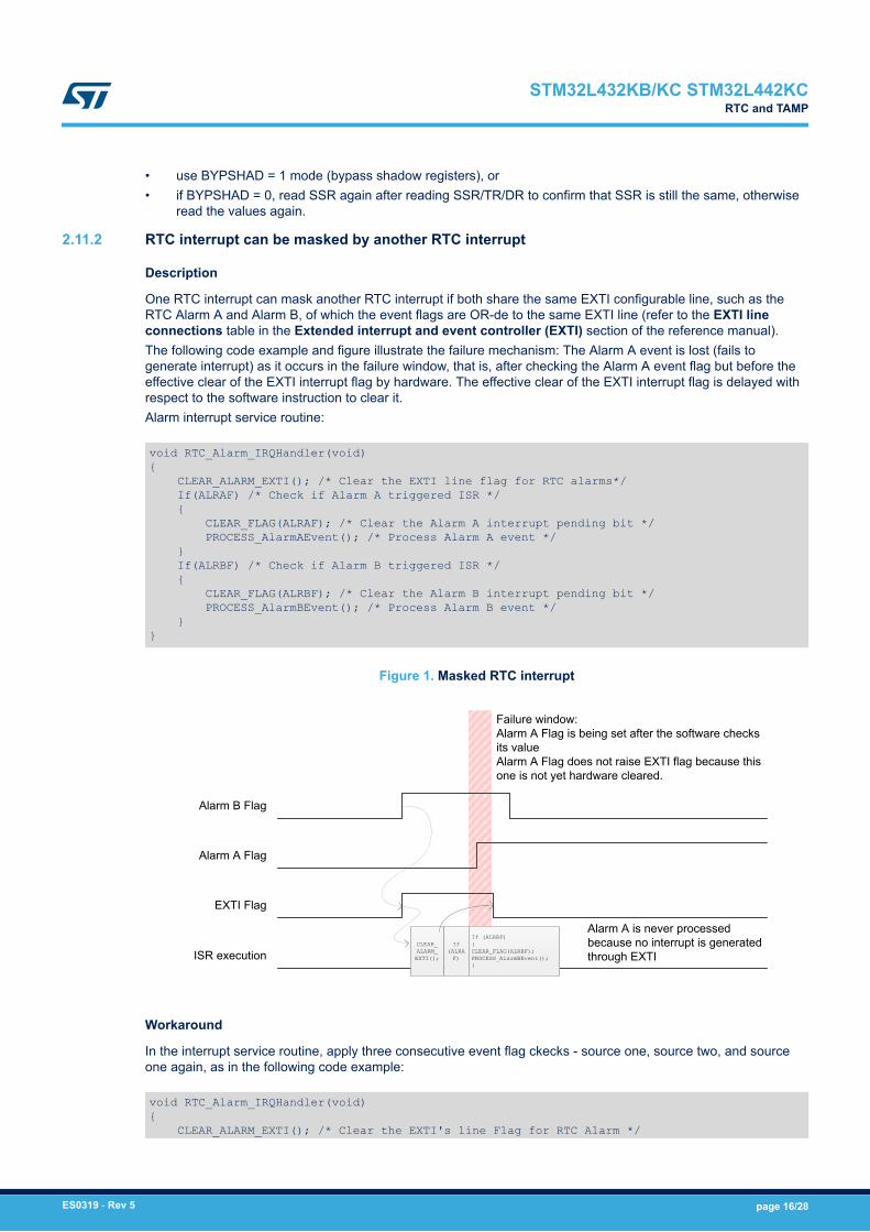
2.11.2 RTC interrupt can be masked by another RTC interrupt
Description
One RTC interrupt can mask another RTC interrupt if both share the same EXTI configurable line, such as theRTC Alarm A and Alarm B, of which the event flags are OR-de to the same EXTI line (refer to the EXTI lineconnections table in the Extended interrupt and event controller (EXTI) section of the reference manual).The following code example and figure illustrate the failure mechanism: The Alarm A event is lost (fails togenerate interrupt) as it occurs in the failure window, that is, after checking the Alarm A event flag but before theeffective clear of the EXTI interrupt flag by hardware. The effective clear of the EXTI interrupt flag is delayed withrespect to the software instruction to clear it.Alarm interrupt service routine:
void RTC_Alarm_IRQHandler(void){ CLEAR_ALARM_EXTI(); /* Clear the EXTI line flag for RTC alarms*/ If(ALRAF) /* Check if Alarm A triggered ISR */ { CLEAR_FLAG(ALRAF); /* Clear the Alarm A interrupt pending bit */ PROCESS_AlarmAEvent(); /* Process Alarm A event */ } If(ALRBF) /* Check if Alarm B triggered ISR */ { CLEAR_FLAG(ALRBF); /* Clear the Alarm B interrupt pending bit */ PROCESS_AlarmBEvent(); /* Process Alarm B event */ }}
Figure 1. Masked RTC interrupt
Alarm B Flag
Alarm A Flag
EXTI Flag
ISR executionCLEAR_ALARM_EXTI();
If (ALRAF)
If (ALRBF){CLEAR_FLAG(ALRBF);PROCESS_AlarmBEvent();}
Failure window: Alarm A Flag is being set after the software checks its valueAlarm A Flag does not raise EXTI flag because this one is not yet hardware cleared.
Alarm A is never processed because no interrupt is generated through EXTI
Workaround
In the interrupt service routine, apply three consecutive event flag ckecks - source one, source two, and sourceone again, as in the following code example:
void RTC_Alarm_IRQHandler(void){ CLEAR_ALARM_EXTI(); /* Clear the EXTI's line Flag for RTC Alarm */
STM32L432KB/KC STM32L442KCRTC and TAMP
ES0319 - Rev 5 page 16/28

If(ALRAF) /* Check if AlarmA triggered ISR */ { CLEAR_FLAG(ALRAF); /* Clear the AlarmA interrupt pending bit */ PROCESS_AlarmAEvent(); /* Process AlarmA Event */ } If(ALRBF) /* Check if AlarmB triggered ISR */ { CLEAR_FLAG(ALRBF); /* Clear the AlarmB interrupt pending bit */ PROCESS_AlarmBEvent(); /* Process AlarmB Event */ } If(ALRAF) /* Check if AlarmA triggered ISR */ { CLEAR_FLAG(ALRAF); /* Clear the AlarmA interrupt pending bit */ PROCESS_AlarmAEvent(); /* Process AlarmA Event */ }}
2.11.3 Calendar initialization may fail in case of consecutive INIT mode entry
Description
If the INIT bit of the RTC_ISR register is set between one and two RTCCLK cycles after being cleared, the INITFflag is set immediately instead of waiting for synchronization delay (which should be between one and twoRTCCLK cycles), and the initialization of registers may fail.Depending on the INIT bit clearing and setting instants versus the RTCCLK edges, it can happen that, after beingimmediately set, the INITF flag is cleared during one RTCCLK period then set again. As writes to calendarregisters are ignored when INITF is low, a write during this critical period might result in the corruption of one ormore calendar registers.
Workaround
After existing the initialization mode, clear the BYPSHAD bit (if set) then wait for RSF to rise, before entering theinitialization mode again.
Note: It is recommended to write all registers in a single initialization session to avoid accumulating synchronizationdelays.
2.11.4 RTC_REFIN and RTC_OUT on PB2 not operating in Stop 2 mode
Description
In Stop 2 low‑power mode, the RTC_REFIN function does not operate and the RTC_OUT function does notoperate if mapped on the PB2 pin.
Workaround
Apply one of the following measures:• Use Stop 1 mode instead of Stop 2. This ensures the operation of both functions.• Map RTC_OUT to the PC13 pin. This ensures the operation of the RTC_OUT function in either low-power
mode. However, it has no effect to the RTC_REFIN function.
2.11.5 Setting GPIO properties of PC13 used as RTC_ALARM open-drain output
Description
Some reference manual revisions may omit the information that the PC13 GPIO must be set as input when theRTC_OR register configures PC13 as open‑drain output of the RTC_ALARM signal.
Note: Enabling the internal pull-up function through the PC13 GPIO settings allows sparing an external pull-up resistor.This is a documentation issue rather than a product limitation.
Workaround
No application workaround is required provided that the described GPIO setting is respected.
STM32L432KB/KC STM32L442KCRTC and TAMP
ES0319 - Rev 5 page 17/28

2.12 I2C
2.12.1 10-bit master mode: new transfer cannot be launched if first part of the address is notacknowledged by the slave
Description
An I2C-bus master generates STOP condition upon non-acknowledge of I2C address that it sends. This applies to7-bit address as well as to each byte of 10-bit address.When the MCU set as I2C-bus master transmits a 10-bit address of which the first byte (5-bit header + 2 MSBs ofthe address + direction bit) is not acknowledged, the MCU duly generates STOP condition but it then cannot startany new I2C-bus transfer. In this spurious state, the NACKF flag of the I2C_ISR register and the START bit of theI2C_CR2 register are both set, while the START bit should normally be cleared.
Workaround
In 10-bit-address master mode, if both NACKF flag and START bit get simultaneously set, proceed as follows:1. Wait for the STOP condition detection (STOPF = 1 in I2C_ISR register).2. Disable the I2C peripheral.3. Wait for a minimum of three APB cycles.4. Enable the I2C peripheral again.
2.12.2 Wrong behavior in Stop mode when wakeup from Stop mode is disabled in I2C
Description
If the wakeup from Stop mode by I2C is disabled (WUPEN = 0), the correct use of the I2C peripheral is to disableit (PE = 0) before entering Stop mode, and re-enable it when back in Run mode.Some reference manual revisions may omit this information.Failure to respect the above while the MCU operating as slave or as master in multi-master topology enters Stopmode during a transfer ongoing on the I2C-bus may lead to the following:1. BUSY flag is wrongly set when the MCU exits Stop mode. This prevents from initiating a transfer in master
mode, as the START condition cannot be sent when BUSY is set.2. If clock stretching is enabled (NOSTRETCH = 0), the SCL line is pulled low by I2C and the transfer stalled
as long as the MCU remains in Stop mode.The occurrence of such condition depends on the timing configuration, peripheral clock frequency, and I2C-bus frequency.
This is a description inaccuracy issue rather than a product limitation.
Workaround
No application workaround is required.
2.12.3 Wrong data sampling when data setup time (tSU;DAT) is shorter than one I2C kernel clock period
Description
The I2C-bus specification and user manual specify a minimum data setup time (tSU;DAT) as:• 250 ns in Standard mode• 100 ns in Fast mode• 50 ns in Fast mode Plus
The MCU does not correctly sample the I2C-bus SDA line when tSU;DAT is smaller than one I2C kernel clock (I2C-bus peripheral clock) period: the previous SDA value is sampled instead of the current one. This can result in awrong receipt of slave address, data byte, or acknowledge bit.
STM32L432KB/KC STM32L442KCI2C
ES0319 - Rev 5 page 18/28

Workaround
Increase the I2C kernel clock frequency to get I2C kernel clock period within the transmitter minimum data setuptime. Alternatively, increase transmitter’s minimum data setup time. If the transmitter setup time minimum valuecorresponds to the minimum value provided in the I2C-bus standard, the minimum I2CCLK frequencies are asfollows:• In Standard mode, if the transmitter minimum setup time is 250 ns, the I2CCLK frequency must be at least 4
MHz.• In Fast mode, if the transmitter minimum setup time is 100 ns, the I2CCLK frequency must be at least 10
MHz.• In Fast-mode Plus, if the transmitter minimum setup time is 50 ns, the I2CCLK frequency must be at least 20
MHz.
2.12.4 Spurious bus error detection in master mode
Description
In master mode, a bus error can be detected spuriously, with the consequence of setting the BERR flag of theI2C_SR register and generating bus error interrupt if such interrupt is enabled. Detection of bus error has noeffect on the I2C-bus transfer in master mode and any such transfer continues normally.
Workaround
If a bus error interrupt is generated in master mode, the BERR flag must be cleared by software. No other actionis required and the ongoing transfer can be handled normally.
2.12.5 Last-received byte loss in reload mode
Description
If in master receiver mode or slave receive mode with SBC = 1 the following conditions are all met:• I2C-bus stretching is enabled (NOSTRETCH = 0)• RELOAD bit of the I2C_CR2 register is set• NBYTES bitfield of the I2C_CR2 register is set to N greater than 1• byte N is received on the I2C-bus, raising the TCR flag• N - 1 byte is not yet read out from the data register at the instant TCR is raised,
then the SCL line is pulled low (I2C-bus clock stretching) and the transfer of the byte N from the shift register tothe data register inhibited until the byte N-1 is read and NBYTES bitfield reloaded with a new value, the latter ofwhich also clears the TCR flag. As a consequence, the software cannot get the byte N and use its content beforesetting the new value into the NBYTES field.For I2C instances with independent clock, the last-received data is definitively lost (never transferred from theshift register to the data register) if the data N - 1 is read within four APB clock cycles preceding the receipt of thelast data bit of byte N and thus the TCR flag raising. Refer to the product reference manual or datasheet for theI2C implementation table.
Workaround
• In master mode or in slave mode with SBC = 1, use the reload mode with NBYTES = 1.• In master receiver mode, if the number of bytes to transfer is greater than 255, do not use the reload mode.
Instead, split the transfer into sections not exceeding 255 bytes and separate them with repeated STARTconditions.
• Make sure, for example through the use of DMA, that the byte N - 1 is always read before the TCR flag israised. Specifically for I2C instances with independent clock, make sure that it is always read earlier thanfour APB clock cycles before the receipt of the last data bit of byte N and thus the TCR flag raising.
The last workaround in the list must be evaluated carefully for each application as the timing depends on factorssuch as the bus speed, interrupt management, software processing latencies, and DMA channel priority.
STM32L432KB/KC STM32L442KCI2C
ES0319 - Rev 5 page 19/28

2.12.6 Spurious master transfer upon own slave address match
Description
When the device is configured to operate at the same time as master and slave (in a multi- master I2C-busapplication), a spurious master transfer may occur under the following condition:• Another master on the bus is in process of sending the slave address of the device (the bus is busy).• The device initiates a master transfer by bit set before the slave address match event (the ADDR flag set in
the I2C_ISR register) occurs.• After the ADDR flag is set:
– the device does not write I2C_CR2 before clearing the ADDR flag, or– the device writes I2C_CR2 earlier than three I2C kernel clock cycles before clearing the ADDR flag
In these circumstances, even though the START bit is automatically cleared by the circuitry handling the ADDRflag, the device spuriously proceeds to the master transfer as soon as the bus becomes free. The transferconfiguration depends on the content of the I2C_CR2 register when the master transfer starts. Moreover, if theI2C_CR2 is written less than three kernel clocks before the ADDR flag is cleared, the I2C peripheral may fall intoan unpredictable state.
Workaround
Upon the address match event (ADDR flag set), apply the following sequence.Normal mode (SBC = 0):1. Set the ADDRCF bit.2. Before Stop condition occurs on the bus, write I2C_CR2 with the START bit low.Slave byte control mode (SBC = 1):1. Write I2C_CR2 with the slave transfer configuration and the START bit low.2. Wait for longer than three I2C kernel clock cycles.3. Set the ADDRCF bit.4. Before Stop condition occurs on the bus, write I2C_CR2 again with its current value.The time for the software application to write the I2C_CR2 register before the Stop condition is limited, as theclock stretching (if enabled), is aborted when clearing the ADDR flag.Polling the BUSY flag before requesting the master transfer is not a reliable workaround as the bus may becomebusy between the BUSY flag check and the write into the I2C_CR2 register with the START bit set.
2.13 USART
2.13.1 RTS is active while RE = 0 or UE = 0
Description
The RTS line is driven low as soon as RTSE bit is set, even if the USART is disabled (UE = 0) or the receiver isdisabled (RE = 0), that is, not ready to receive data.
Workaround
Upon setting the UE and RE bits, configure the I/O used for RTS into alternate function.
2.14 LPUART
2.14.1 LPUART1 outputs cannot be configured as open‑drain
Description
LPUART1 outputs are set in push‑pull mode regardless of the configuration of corresponding GPIO outputs.
STM32L432KB/KC STM32L442KCUSART
ES0319 - Rev 5 page 20/28

Workaround
None.
2.15 SPI
2.15.1 BSY bit may stay high at the end of data transfer in slave mode
Description
BSY flag may sporadically remain high at the end of a data transfer in slave mode. This occurs upon coincidenceof internal CPU clock and external SCK clock provided by master.In such an event, if the software only relies on BSY flag to detect the end of SPI slave data transaction (forexample to enter low-power mode or to change data line direction in half-duplex bidirectional mode), the detectionfails.As a conclusion, the BSY flag is unreliable for detecting the end of data transactions.
Workaround
Depending on SPI operating mode, use the following means for detecting the end of transaction:• When NSS hardware management is applied and NSS signal is provided by master, use NSS flag.• In SPI receiving mode, use the corresponding RXNE event flag.• In SPI transmit-only mode, use the BSY flag in conjunction with a timeout expiry event. Set the timeout such
as to exceed the expected duration of the last data frame and start it upon TXE event that occurs with thesecond bit of the last data frame. The end of the transaction corresponds to either the BSY flag becominglow or the timeout expiry, whichever happens first.
Prefer one of the first two measures to the third as they are simpler and less constraining.Alternatively, apply the following sequence to ensure reliable operation of the BSY flag in SPI transmit mode:1. Write last data to data register.2. Poll the TXE flag until it becomes high, which occurs with the second bit of the data frame transfer.3. Disable SPI by clearing the SPE bit mandatorily before the end of the frame transfer.4. Poll the BSY bit until it becomes low, which signals the end of transfer.
Note: The alternative method can only be used with relatively fast CPU speeds versus relatively slow SPI clocksor/and long last data frames. The faster is the software execution, the shorter can be the duration of the last dataframe.
2.15.2 Wrong CRC in full-duplex mode handled by DMA with imbalanced setting of data counters
Description
When SPI is handled by DMA in full-duplex master or slave mode with CRC enabled, the CRC computation maytemporarily freeze for the ongoing frame, which results in corrupted CRC.This happens when the receive counter reaches zero upon the receipt of the CRC pattern (as the receive counterwas set to a value greater, by CRC length, than the transmit counter). An internal signal dedicated to receive-onlymode is left unduly pending. Consequently, the signal can cause the CRC computation to freeze during a nexttransaction in which DMA TXE event service is accidentally delayed (for example, due to DMA servicing a requestfrom another channel).
Workaround
Apply one of the following measures prior to each full-duplex SPI transaction:• Set the DMA transmission and reception data counters to equal values. Upon the transaction completion,
read the CRC pattern out from RxFIFO separately by software.• Reset the SPI peripheral via peripheral reset register.
STM32L432KB/KC STM32L442KCSPI
ES0319 - Rev 5 page 21/28

2.15.3 CRC error in SPI slave mode if internal NSS changes before CRC transfer
Description
Some reference manual revisions may omit the information that the device operating as SPI slave must beconfigured in software NSS control if the SPI master pulses the NSS (for (for example in NSS pulse mode).Otherwise, the transition of the internal NSS signal after the CRCNEXT flag is set might result in wrong CRCvalue computed by the device and, as a consequence, in a CRC error. As a consequence, the NSS pulse modecannot be used along with the CRC function.This is a documentation error rather than a product limitation.
Workaround
No application workaround is required as long as the device operating as SPI slave is duly configured in softwareNSS control.
2.15.4 SPI master communication failure at high fPCLK within the specified range
Description
The SPI peripheral configured as master, with the SPIx_CR1 register's CPHA bit set and BR[2:0] bitfield writtenwith 001 (fPCLK/4), may spuriously generate an extra clock pulse at the end of the last data frame to transfer (atthe end of which the clock is expected to stop) if the PCLK frequency exceeds the values as per the table. Thisleads to a desynchronization of the SPI data flow.
Table 6. Maximum fPCLK for safe SPI operation
SPI instancefPCLK(max) [MHz]
Range 1 Range 2
SPI1 65.1 >26 (OK)
SPI3 60.2 >26 (OK)
Workaround
None.
2.16 bxCAN
2.16.1 bxCAN time-triggered communication mode not supported
Description
The time-triggered communication mode described in the reference manual is not supported. As a result,timestamp values are not available. The TTCM of the CAN_MCR register must be kept cleared (time-triggeredcommunication mode disabled).
Workaround
None.
STM32L432KB/KC STM32L442KCbxCAN
ES0319 - Rev 5 page 22/28

Revision history
Table 7. Document revision history
Date Version Changes
18-Apr-2016 1 Initial release.
05-Sep-2016 2
Added:• PCPROP area within a single Flash memory page becomes
unprotected at RDP change from level1 to level0• Spurious bus error detection in master mode• Inhibited acquisition in short transfer phase configuration• STM32L432KB part number
05-Dec-2016 3
Added:• Silicon revision Z• MSI frequency overshoot upon Stop mode exit• Internal voltage reference corrupted upon Stop mode entry with
temperature sensing enabled• Wrong data can be read in memory-mapped after an indirect mode
operation• First nibble of data is not written after dummy phase• 10-bit master mode: new transfer cannot be launched if first part of the
address has not been acknowledged by the slave
Modified:• Document structure: cover page, titles, legend, removal of the list of
tables, Table 3: Summary of device limitations• The order of functions aligned with the reference manual• JTAG function replaced with more general DBG• BSY bit may stay high at the end of a data transfer in slave mode
27-Nov-2018 4
Added:• Table of documentation errata• Section 2.1.2 VDIV or VSQRT instructions might not complete
correctly when very short ISRs are used• Section 2.1.3 Store immediate overlapping exception return operation
might vector to incorrect interrupt• Section 2.2.8 Unstable LSI when it clocks RTC or CSS on LSE• Section 2.2.10 First double‑word of Flash memory corrupted upon
reset or power-down while programming• Section 2.3 FW with Code segment unprotected if non-volatile data
segment length is zero• Section 2.5.1 Writing ADCx_JSQR when JADCSTART and JQDIS are
set might lead to incorrect behavior• Section 2.8.3 CCM authentication mode not compliant with NIST
CMAC to Section 2.8.5 Wait until BUSY is low when suspending GCMencryption
• Section 2.5.3 Spurious temperature measurement due to spike noise• Section 2.10.1 MCU may remain stuck in LPTIM interrupt when
entering Stop mode• Section 2.11 RTC and TAMP with four limitations and one
documentation erratum• Section 2.12.5 Last-received byte loss in reload mode
STM32L432KB/KC STM32L442KC
ES0319 - Rev 5 page 23/28

Date Version Changes
27-Nov-2018 4 (continued)
Added:• Section 2.12.6 Spurious master transfer upon own slave address
match• Section 2.13 USART with RTS is active while RE = 0 or UE = 0• Section 2.15.2 Wrong CRC in full-duplex mode handled by DMA with
imbalanced setting of data counters• Section 2.15.3 CRC error in SPI slave mode if internal NSS changes
before CRC transfer
Modified:• HSI48 ready interrupt capability is not supported and Full JTAG
configuration without NJTRST pin cannot be used moved to Section 2.2 System
• Section 2.4.2 Wrong data from memory-mapped read after an indirectmode operation
• Section 2.5.2 Wrong ADC result if conversion done late aftercalibration or previous conversion
• Section 2.8.1 Burst read or write accesses not supported and Section 2.8.2 TAG computation in GCM encryption mode moved todocumentation errata table
• Section 2.12.2 Wrong behavior in Stop mode when wakeup from Stopmode is disabled in I2C and Section 2.7.1 Inhibited acquisition in shorttransfer phase configuration modified and moved to documentationerrata table
31-Jul-2019 5
Added:• Section 2.2.5 Spurious brown-out reset after short run sequence• Section 2.15.4 SPI master communication failure at high fPCLK within
the specified range
Modified:• reference to Current injection from VDD to VDDA through analog switch
voltage booster added to Table 2
STM32L432KB/KC STM32L442KC
ES0319 - Rev 5 page 24/28

Contents
1 Summary of device errata. . . . . . . . . . . . . . . . . . . . . . . . . . . . . . . . . . . . . . . . . . . . . . . . . . . . . . . . . .2
2 Description of device errata. . . . . . . . . . . . . . . . . . . . . . . . . . . . . . . . . . . . . . . . . . . . . . . . . . . . . . . .4
2.1 Core . . . . . . . . . . . . . . . . . . . . . . . . . . . . . . . . . . . . . . . . . . . . . . . . . . . . . . . . . . . . . . . . . . . . . . . . . 4
2.1.1 Interrupted loads to SP can cause erroneous behavior . . . . . . . . . . . . . . . . . . . . . . . . . . . . 4
2.1.2 VDIV or VSQRT instructions might not complete correctly when very short ISRs are used . 4
2.1.3 Store immediate overlapping exception return operation might vector to incorrect interrupt 5
2.2 System . . . . . . . . . . . . . . . . . . . . . . . . . . . . . . . . . . . . . . . . . . . . . . . . . . . . . . . . . . . . . . . . . . . . . . . 6
2.2.1 MSIRDY flag issue preventing entry in low-power mode . . . . . . . . . . . . . . . . . . . . . . . . . . . 6
2.2.2 PCPROP area within a single Flash memory page becomes unprotected at RDP changefrom Level 1 to Level 0 . . . . . . . . . . . . . . . . . . . . . . . . . . . . . . . . . . . . . . . . . . . . . . . . . . . . 6
2.2.3 MSI frequency overshoot upon Stop mode exit . . . . . . . . . . . . . . . . . . . . . . . . . . . . . . . . . . 7
2.2.4 Internal voltage reference corrupted upon Stop mode entry with temperature sensingenabled . . . . . . . . . . . . . . . . . . . . . . . . . . . . . . . . . . . . . . . . . . . . . . . . . . . . . . . . . . . . . . . . 7
2.2.5 Spurious brown-out reset after short run sequence. . . . . . . . . . . . . . . . . . . . . . . . . . . . . . . 8
2.2.6 Full JTAG configuration without NJTRST pin cannot be used . . . . . . . . . . . . . . . . . . . . . . . 8
2.2.7 Current injection from VDD to VDDA through analog switch voltage booster. . . . . . . . . . . . . 8
2.2.8 Unstable LSI when it clocks RTC or CSS on LSE . . . . . . . . . . . . . . . . . . . . . . . . . . . . . . . . 9
2.2.9 HSI48 ready interrupt capability is not supported . . . . . . . . . . . . . . . . . . . . . . . . . . . . . . . . 9
2.2.10 First double‑word of Flash memory corrupted upon reset or power-down whileprogramming. . . . . . . . . . . . . . . . . . . . . . . . . . . . . . . . . . . . . . . . . . . . . . . . . . . . . . . . . . . . 9
2.3 FW . . . . . . . . . . . . . . . . . . . . . . . . . . . . . . . . . . . . . . . . . . . . . . . . . . . . . . . . . . . . . . . . . . . . . . . . . 10
2.3.1 Code segment unprotected if non-volatile data segment length is zero. . . . . . . . . . . . . . . 10
2.4 QUADSPI . . . . . . . . . . . . . . . . . . . . . . . . . . . . . . . . . . . . . . . . . . . . . . . . . . . . . . . . . . . . . . . . . . . . 10
2.4.1 First nibble of data not written after dummy phase . . . . . . . . . . . . . . . . . . . . . . . . . . . . . . 10
2.4.2 Wrong data from memory-mapped read after an indirect mode operation. . . . . . . . . . . . . 11
2.5 ADC . . . . . . . . . . . . . . . . . . . . . . . . . . . . . . . . . . . . . . . . . . . . . . . . . . . . . . . . . . . . . . . . . . . . . . . . 11
2.5.1 Writing ADCx_JSQR when JADCSTART and JQDIS are set might lead to incorrectbehavior . . . . . . . . . . . . . . . . . . . . . . . . . . . . . . . . . . . . . . . . . . . . . . . . . . . . . . . . . . . . . . 11
2.5.2 Wrong ADC result if conversion done late after calibration or previous conversion . . . . . . 11
2.5.3 Spurious temperature measurement due to spike noise . . . . . . . . . . . . . . . . . . . . . . . . . . 11
2.6 COMP. . . . . . . . . . . . . . . . . . . . . . . . . . . . . . . . . . . . . . . . . . . . . . . . . . . . . . . . . . . . . . . . . . . . . . . 12
2.6.1 Comparator outputs cannot be configured in open-drain. . . . . . . . . . . . . . . . . . . . . . . . . . 12
STM32L432KB/KC STM32L442KCContents
ES0319 - Rev 5 page 25/28

2.6.2 COMP1 and COMP2 configuration lost with software reset. . . . . . . . . . . . . . . . . . . . . . . . 12
2.7 TSC. . . . . . . . . . . . . . . . . . . . . . . . . . . . . . . . . . . . . . . . . . . . . . . . . . . . . . . . . . . . . . . . . . . . . . . . . 12
2.7.1 Inhibited acquisition in short transfer phase configuration . . . . . . . . . . . . . . . . . . . . . . . . . 12
2.8 AES. . . . . . . . . . . . . . . . . . . . . . . . . . . . . . . . . . . . . . . . . . . . . . . . . . . . . . . . . . . . . . . . . . . . . . . . . 13
2.8.1 Burst read or write accesses not supported . . . . . . . . . . . . . . . . . . . . . . . . . . . . . . . . . . . 13
2.8.2 TAG computation in GCM encryption mode . . . . . . . . . . . . . . . . . . . . . . . . . . . . . . . . . . . 13
2.8.3 CCM authentication mode not compliant with NIST CMAC . . . . . . . . . . . . . . . . . . . . . . . . 13
2.8.4 Datatype initial configuration in GCM mode . . . . . . . . . . . . . . . . . . . . . . . . . . . . . . . . . . . 14
2.8.5 Wait until BUSY is low when suspending GCM encryption . . . . . . . . . . . . . . . . . . . . . . . . 14
2.9 TIM . . . . . . . . . . . . . . . . . . . . . . . . . . . . . . . . . . . . . . . . . . . . . . . . . . . . . . . . . . . . . . . . . . . . . . . . . 14
2.9.1 HSE/32 is not available for TIM16 input capture if RTC clock is disabled or other than HSE.. . . . . . . . . . . . . . . . . . . . . . . . . . . . . . . . . . . . . . . . . . . . . . . . . . . . . . . . . . . . . . . . . . . . . 14
2.10 LPTIM . . . . . . . . . . . . . . . . . . . . . . . . . . . . . . . . . . . . . . . . . . . . . . . . . . . . . . . . . . . . . . . . . . . . . . . 14
2.10.1 MCU may remain stuck in LPTIM interrupt when entering Stop mode. . . . . . . . . . . . . . . . 14
2.10.2 MCU may remain stuck in LPTIM interrupt when clearing event flag. . . . . . . . . . . . . . . . . 15
2.10.3 LPTIM1 outputs cannot be configured as open‑drain . . . . . . . . . . . . . . . . . . . . . . . . . . . . 15
2.11 RTC and TAMP . . . . . . . . . . . . . . . . . . . . . . . . . . . . . . . . . . . . . . . . . . . . . . . . . . . . . . . . . . . . . . . 15
2.11.1 RTC calendar registers are not locked properly . . . . . . . . . . . . . . . . . . . . . . . . . . . . . . . . 15
2.11.2 RTC interrupt can be masked by another RTC interrupt . . . . . . . . . . . . . . . . . . . . . . . . . . 16
2.11.3 Calendar initialization may fail in case of consecutive INIT mode entry . . . . . . . . . . . . . . . 17
2.11.4 RTC_REFIN and RTC_OUT on PB2 not operating in Stop 2 mode . . . . . . . . . . . . . . . . . 17
2.11.5 Setting GPIO properties of PC13 used as RTC_ALARM open-drain output . . . . . . . . . . . 17
2.12 I2C . . . . . . . . . . . . . . . . . . . . . . . . . . . . . . . . . . . . . . . . . . . . . . . . . . . . . . . . . . . . . . . . . . . . . . . . . 17
2.12.1 10-bit master mode: new transfer cannot be launched if first part of the address is notacknowledged by the slave . . . . . . . . . . . . . . . . . . . . . . . . . . . . . . . . . . . . . . . . . . . . . . . . 18
2.12.2 Wrong behavior in Stop mode when wakeup from Stop mode is disabled in I2C . . . . . . . 18
2.12.3 Wrong data sampling when data setup time (tSU;DAT) is shorter than one I2C kernel clockperiod . . . . . . . . . . . . . . . . . . . . . . . . . . . . . . . . . . . . . . . . . . . . . . . . . . . . . . . . . . . . . . . . 18
2.12.4 Spurious bus error detection in master mode . . . . . . . . . . . . . . . . . . . . . . . . . . . . . . . . . . 19
2.12.5 Last-received byte loss in reload mode . . . . . . . . . . . . . . . . . . . . . . . . . . . . . . . . . . . . . . . 19
2.12.6 Spurious master transfer upon own slave address match . . . . . . . . . . . . . . . . . . . . . . . . . 19
2.13 USART . . . . . . . . . . . . . . . . . . . . . . . . . . . . . . . . . . . . . . . . . . . . . . . . . . . . . . . . . . . . . . . . . . . . . . 20
2.13.1 RTS is active while RE = 0 or UE = 0 . . . . . . . . . . . . . . . . . . . . . . . . . . . . . . . . . . . . . . . . 20
STM32L432KB/KC STM32L442KCContents
ES0319 - Rev 5 page 26/28

2.14 LPUART . . . . . . . . . . . . . . . . . . . . . . . . . . . . . . . . . . . . . . . . . . . . . . . . . . . . . . . . . . . . . . . . . . . . . 20
2.14.1 LPUART1 outputs cannot be configured as open‑drain. . . . . . . . . . . . . . . . . . . . . . . . . . . 20
2.15 SPI . . . . . . . . . . . . . . . . . . . . . . . . . . . . . . . . . . . . . . . . . . . . . . . . . . . . . . . . . . . . . . . . . . . . . . . . . 21
2.15.1 BSY bit may stay high at the end of data transfer in slave mode. . . . . . . . . . . . . . . . . . . . 21
2.15.2 Wrong CRC in full-duplex mode handled by DMA with imbalanced setting of data counters .. . . . . . . . . . . . . . . . . . . . . . . . . . . . . . . . . . . . . . . . . . . . . . . . . . . . . . . . . . . . . . . . . . . . . 21
2.15.3 CRC error in SPI slave mode if internal NSS changes before CRC transfer . . . . . . . . . . . 21
2.15.4 SPI master communication failure at high fPCLK within the specified range . . . . . . . . . . . . 22
2.16 bxCAN . . . . . . . . . . . . . . . . . . . . . . . . . . . . . . . . . . . . . . . . . . . . . . . . . . . . . . . . . . . . . . . . . . . . . . 22
2.16.1 bxCAN time-triggered communication mode not supported. . . . . . . . . . . . . . . . . . . . . . . . 22
Revision history . . . . . . . . . . . . . . . . . . . . . . . . . . . . . . . . . . . . . . . . . . . . . . . . . . . . . . . . . . . . . . . . . . . . . . .23
STM32L432KB/KC STM32L442KCContents
ES0319 - Rev 5 page 27/28

IMPORTANT NOTICE – PLEASE READ CAREFULLY
STMicroelectronics NV and its subsidiaries (“ST”) reserve the right to make changes, corrections, enhancements, modifications, and improvements to STproducts and/or to this document at any time without notice. Purchasers should obtain the latest relevant information on ST products before placing orders. STproducts are sold pursuant to ST’s terms and conditions of sale in place at the time of order acknowledgement.
Purchasers are solely responsible for the choice, selection, and use of ST products and ST assumes no liability for application assistance or the design ofPurchasers’ products.
No license, express or implied, to any intellectual property right is granted by ST herein.
Resale of ST products with provisions different from the information set forth herein shall void any warranty granted by ST for such product.
ST and the ST logo are trademarks of ST. For additional information about ST trademarks, please refer to www.st.com/trademarks. All other product or servicenames are the property of their respective owners.
Information in this document supersedes and replaces information previously supplied in any prior versions of this document.
© 2019 STMicroelectronics – All rights reserved
STM32L432KB/KC STM32L442KC
ES0319 - Rev 5 page 28/28