stmicroelectronics l6717a am3 solution for desktop power
TRANSCRIPT

STMicroelectronicsL6717A AM3 Solution for Desktop Power
AMD CPU Advanced & Green Power Management
Picture frame area
Stanley XING133 1691 5386

This document contains sensitive information. Its distribution is subject to the signature of an Non-Disclosure Agreement (NDA). It is classified “CONFIDENTIAL”
At all times you should comply with the following security rules:Do not copy or reproduce all or part of this document
Keep this document locked awayFurther copies can be provided on a “need to know basis”, please contact your local ST sales office.
Information furnished is believed to be accurate and reliable. However, STMicroelectronics assumes no responsibility for the consequences of use of such information nor for any infringement of patents or other rights of third parties which may result from its use. No license is granted by implication or otherwise under any patent or patent rights of STMicroelectronics. Specifications mentioned in this publication are subject to change without
notice. This publication supersedes and replaces all information previously supplied. STMicroelectronics products are not authorized for use as critical components in life support devices or systems without express
written approval of STMicroelectronics.
The ST logo is a registered trademark of STMicroelectronics.All other names are the property of their respective owners
© 2009 STMicroelectronics - All rights reserved
STMicroelectronics GROUP OF COMPANIESAustralia - Belgium - Brazil - Canada - China - Czech Republic - Finland - France - Germany - Hong Kong - India - Israel - Italy - Japan - Malaysia - Malta - Morocco - Singapore - Spain - Sweden - Switzerland - United Kingdom
- United States
Confidentiality Obligations
Agenda
STMicroelectronics vs. AMD AlignmentST L6717 Power Solution
Pin Assignment & Reference SchematicIC Operation & ConfigurationLTB SnapshotI2C Interface for Power Management
Demo Board OverviewController Details: LTB Technology ®
XLS Design Tools & SVI-I2C Interface SW

SVI 2RailsSVI 2Rails
ST Alignment with AMD Platforms
SocketSocket
TDPTDP
DC = 110W / 80AFX = 104W / 80ASC = 89W / 60A
FX = 125W / 95ADC = 104W / 80ASC = 72W / 60A
QC = 140W / 110AQC = 125W / 95ADC = 89W / 80ASC = 45W / 45A
PVI / SVIPVI / SVI
5bit PVI 1Rail5bit PVI 1Rail
6bit PVI 1Rail6bit PVI 1Rail
L6717, L6740L (L6717, L6740L (11stst Hybrid Regulator Hybrid Regulator ) ) –– (4+1) Phase Controller(4+1) Phase Controller
L6713A, L6714 L6713A, L6714 –– 3 / 4 Phase Controllers 3 / 4 Phase Controllers -- PVIPVI
H / >H
Socket M3Socket M3
QC = 140W / 110AQC = 125W / 95ADC = 89W / 80ASC = 45W / 45A

ST DT/Server AM2r2/Fr2 Solutions ST L6713A, L6714ST L6713A, L6714 ST L6740LST L6740L
PVI ArchitecturePVI Architecture2 to 3/4 Phase ControllerEmbedded Drivers Arch.LTB Technology®
OVP, OCP, FB_DISC10x10 HTQFP64
Hybrid ControllerHybrid Controller2 to 4Ph CORE + 1Ph NBPVI / SVI CompatibilityPSI_L ManagementLTB Technology®
OVP, OCP, FB_DISC7x7 HTQFP48
L6740LL6740L(Hybrid)(Hybrid)
L6741/3L6741/3
L6741/3L6741/3
L6741/3L6741/3
L6741/3L6741/3
L6741/3L6741/3
L6713AL6713A
L6714L6714
ST L6717ST L6717
Hybrid Controller + I2CPMHybrid Controller + I2CPM2 - 4Ph CORE (2Emb + 2PWM)1Ph NB (Emb)PVI / SVI CompatibilityI2C Power ManagerI2C Power ManagerLTB Technology®
7x7 VFQFPN48
L6717L6717(Hybrid)(Hybrid)
L6741/3L6741/3
L6741/3L6741/3
I2CI2C
Agenda
STMicroelectronics vs. AMD AlignmentST L6717 Power Solution
Pin Assignment & Reference SchematicIC Operation & ConfigurationLTB SnapshotI2C Interface for Power Management
Demo Board OverviewController Details: LTB Technology ®
XLS Design Tools & SVI-I2C Interface SW

HIGH CURRENT EMBEDDED DRIVERS (2+1) + 2 ADDITIONAL PWMsPower Manager I2C BusPower Manager I2C Bus
OVP SETUPFSW MARGININGPOWER MANAGEMENT SETUPLL ADJUSTEMENTOVERSPEEDING
AUTOMATIC PVI/SVI CPU DETECTIONEFFICIENCY OPTIMIZATION
DYNAMIC PHASE MANAGEMENT (DPM)LTB Technology®
DUAL DIFFERENTIAL REMOTE SENSEDIFFERENTIAL CURRENT SENSE for both CORE & NBCORE DUAL OCP THRESHOLD: PER-PHASE AND TOTAL CURRENTPRE-BIAS STATUP MANAGEMENTFEEDBACK DISCONNECTION PROTECTIONVFQFPN48 (7x7mm) PACKAGE
L6717 – Hybrid Controller with Power Manager I2C
L6717

L6717 – Application Block Diagram
L6717L6717
L6741/3L6741/3
L6741/3L6741/3
NBNB
CORECORE
SVI / PVI bus SVI / PVI bus
DDRDDR
HTHT
Secondary I2C bus for ST Power Manager;Secondary I2C bus for ST Power Manager;Allows RealAllows Real--Time OverTime Over--speed, Fsw Modification, Phase Sheddingspeed, Fsw Modification, Phase Shedding……

Agenda
STMicroelectronics vs. AMD AlignmentST L6717 Power Solution
Pin Assignment & Reference SchematicIC Operation & ConfigurationLTB SnapshotI2C Interface for Power Management
Demo Board Overview Controller Details: LTB Technology ®
XLS Design Tools & SVI-I2C Interface SW

PHASE NUMBER Selection & Interleaving (1)4
PHA
SE
3 PH
ASE
2 PH
ASE
3 Phase OperationPWM4 = SGNDCS4+ connected to VCORECS4- VCORE by same RG of other channels
2 Phase Operation (see next slide)PWM3 & PWM4 = SGNDCS3+ & CS4+ connected to VCORECS3- & CS4- VCORE by same RG of other channels

PHASE NUMBER Selection & Interleaving (2)
2 PHASE Operation CaseThe information on the number of active phases is latched @ EN rise.

SVI/PVI Mode Detection
VDD_NB (HiZ)
VDD_COREVID1=“1”
EN
VDD_NBVDD_COREVID1=“0”
EN
SVI Mode VID1=“0” @ EN Rise
PVI Mode VID1=“1” @ EN Rise
VID[5:0]=[xxxx1x] are decodedto define the bootstrap voltage
VID[2:3]=[xy] are decodedto define the bootstrap voltage

LSLS--Less StartupLess StartupNONO--LSLS--Less StartupLess Startup
LS-Less Start-Up
Allows managing pre-biased output start-upLow-Side MOSFETs are kept OFF until reference = VOUT(depends on ext driver compatibility, need to manage HiZ)No Output Voltage undershoot observable (negative spike)!!

Pre OVP Protection
VCC=5VLGATE
VSEN
EN = 0
Pre-OVPTH = 1.8V
Pre-OVP Protection allow to protect the Load against OVP event also when L6717 is disabled.
VCC and VCCDRV need to be connected to 5V_SBYVSEN is monitored for both CORE & NB section when EN=“0”If VSEN/VSEN_NB rises over 1.8V threshold, corresponding LS Gate will be turned onEN rising edge will reset Pre-OVP and L6717 performs the SSIf OVP condition still present after Pre-OVP and EN rising OVP protection will trigger
EN = “0” PreOVP EN = “0” ”1”

PVI/SVI Soft Start & PGOOD
PGOOD
EN
CORE FB
VCORE
PVI ModePVI Mode SVI ModeSVI Mode
PGOOD
EN
NB FB
CORE FB
PVI Mode•NB is kept in HiZ State;•CORE rise its reference to the finalvoltage according with decoded VID;
•PGOOD is “CORE PGOOD”
SVI Mode•Both CORE and NB perform simultaneous SS;•CORE & NB boot to Pre-POWEROK Metal VID•PGOOD is logic AND of “CORE & NB PGOODs”

Agenda
STMicroelectronics vs. AMD AlignmentST L6717 Power Solution
Pin Assignment, Block Diagram & Reference Schematic OverviewIC Operation and ConfigurationLTB SnapshotI2C Interface for Power Management
Demo Board OverviewController Details: LTB Technology ®
XLS Design Tools & SVI-I2C Interface SW

Fastest response through direct detection of high load Fastest response through direct detection of high load transients,transients,
for cost effective application designfor cost effective application design
Technical Snapshot: LTB Technology®
LTB TechnologyLTB Technology®® further enhances the performances of Dual-Edge Asynchronous Systems
LTB TechnologyLTB Technology®® cancels the interleaved phase-shift, turning-on simultaneously all phases. Asynchronous mode only when necessary, preserving noise immunity
LTB TechnologyLTB Technology®® implements a parallel, independent loop that reacts to Load-Transients bypassing E/A latencies. The LTB Comparator sets the correct amount of transferred energy
With LTB TechnologyLTB Technology®® each Phase is boosted with the correct amount of energy to recover from phase-to-phase asymmetries keeping the phase currents balanced.

The device turns on simultaneously all the phases The device turns on simultaneously all the phases as soon as a load transient is detected ( trough the dedicated as soon as a load transient is detected ( trough the dedicated LTB LTB
pin)pin)
no LTBno LTB LTBLTB
Technical Snapshot: LTB Technology®

Agenda
STMicroelectronics vs. AMD AlignmentST L6717 Power Solution
Pin Assignment, Block Diagram & Reference Schematic OverviewIC Operation and ConfigurationLTB SnapshotI2C Interface for Power Management
Demo Board OverviewController Details: LTB Technology ®
XLS Design Tools & SVI-I2C Interface SW

Agenda
I2C Interface for Power ManagementI2C Protocol OverviewI2C Command DescriptionOS SettingOVP SettingFSW AdjustDroop AdjustDPM (Dynamic Phase Management)
I2C Bus Special FeaturesI2C_ ADDRESS Change (SVI Mode Only)I2C_DISABLE Analog OVP & OS (SVI Mode Only)

I2C Bus: Protocol Overview
I2C Interface is Active by default in both SVI and PVI Mode.I2C Bus & SVI Bus are two Parallel and Independent Interfaces.I2C Commands may be issued by I2C Master once PGOOD is High.
OFFSETOFFSETCORE and/or NBCORE and/or NB
OVPOVPSETTINGSETTING
FSWFSWADJUSTADJUST
DROOPDROOPADJUSTADJUST
POWERPOWERMANAGEMENTMANAGEMENT

Droop AdjustmentDroop AdjustmentModifies the kDRP and kDRPNB to modify the LL without changing external components.Applies to CORE and NB Section.
DRP_ADJDRP_ADJ2+2 data bit2+2 data bit
Fsw AdjustmentFsw AdjustmentModifies the Fsw set by OSC pin by +20%, +10%, 0% (default), -10%, -20%.
FSW_ADJFSW_ADJ+3 data bit+3 data bit
DPMTH DPMTH DPM ThresholdsDPM ThresholdsAllow to define different threshold for DPM transitions.. PSI_A PSI_A PSI ActionPSI ActionDefines the action to take when PSI_L is asserted. #=1 (default) or #=2. PSI_EN PSI_EN PSI ENablePSI ENableEnables (default) or Disables PSI_L (When 0, ignores PSI_L flag from CPU)DPM_EN DPM_EN Dynamic Phase ManagementDynamic Phase Management EnableEnables or Disables (default) DPM mode. (PSI_L flag overrides DPM when asserted.)
PWRMNGPWRMNG2 + 1 data bit2 + 1 data bit+ 1 +1 en bit+ 1 +1 en bit
OVP SetupOVP SetupSets OV threshold above the regulation reference of +250mV (default) with 4x 200mV steps.Section bit defines which section (CORE, NB) the data applies to.
OVP_SETOVP_SET2 +2 data bit2 +2 data bit
OFFSET for OverOFFSET for Over--SpeedingSpeedingSets offset above regulation reference up to 2.8V, 1bit sign+5bit dataApplies to CORE and NB Section (NB only positive and clamped at +600mV)
OVRSPDOVRSPD1 sign +5 data bit1 sign +5 data bit
DescriptionDescriptionCommandCommand
I2C Bus: Command Description

Agenda
I2C Interface for Power ManagementI2C Protocol OverviewI2C Command DescriptionOS SettingOVP SettingFSW AdjustDroop AdjustDPM (Dynamic Phase Management)
I2C Bus Special FeaturesI2C_ ADDRESS Change (SVI Mode Only)I2C_DISABLE Analog OVP & OS (SVI Mode Only)

I2C Bus Special Features: I2C_ADDRESS (SVI Only)
L6717L6717
I2C MasterI2C Master
CORE # 2CORE # 2
L6717L6717
CORE # 1CORE # 1L6717 I2CL6717 I2CADDRESS=ADDRESS=““00””
L6717 I2CL6717 I2CADDRESS=ADDRESS=““11””

I2C Bus Special Features: I2C_DISABLE (SVI Only)
I2C_DISABLE
ANALOG CORE & NB OVP by SDA pin
ANALOG CORE Bidirectional OS by SCL
pin
Agenda
STMicroelectronics vs. AMD AlignmentST L6717 Power Solution
Pin Assignment, Block Diagram & Reference Schematic OverviewPower Up & PVI/SVI SequencingLTB SnapshotI2C Interface for Power Management
Demo Board OverviewController Details: LTB Technology ®
XLS Design Tools & SVI-I2C Interface SW
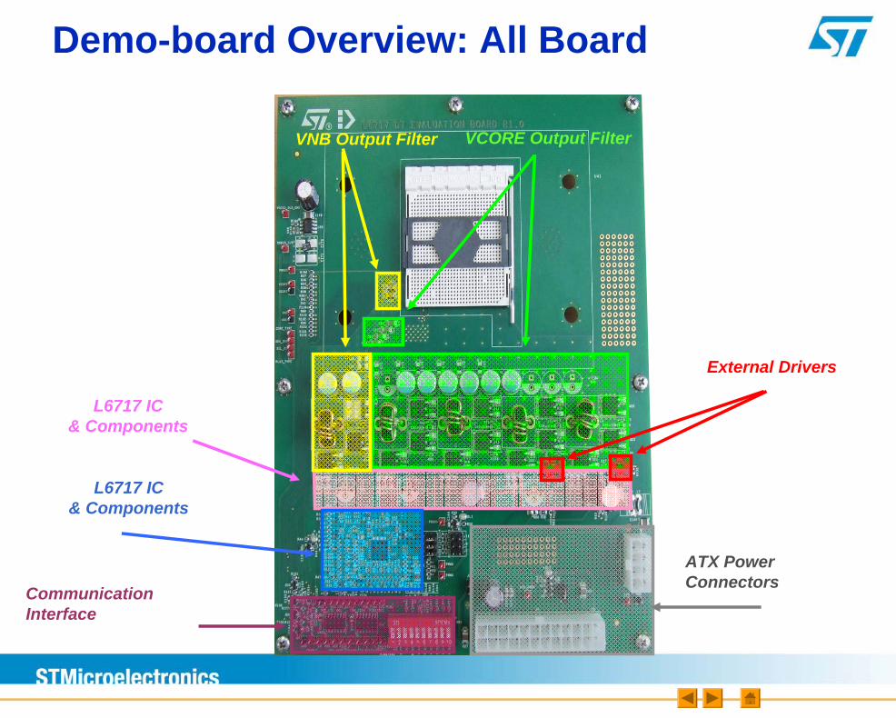
Demo-board Overview: All Board
VCORE Output FilterVNB Output Filter
ATX PowerConnectorsCommunication
Interface
External Drivers
L6717 IC& Components
L6717 IC& Components

Agenda
STMicroelectronics vs. AMD AlignmentST L6717 Power Solution
Pin Assignment & Reference SchematicPower Up & PVI/SVI SequencingLTB SnapshotI2C Interface for Power Management
Demo Board Overview Controller Details: LTB Technology ®
XLS Design Tools & SVI-I2C Interface SW
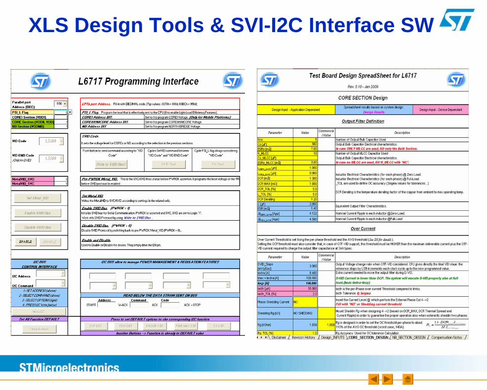
XLS Design Tools & SVI-I2C Interface SW

Q & A…