strategy to realize the euv-fel high power light source ... · fel power with 2% tapering: ......
TRANSCRIPT

Challenges to Realize the EUV-FEL High Power Light Source - Present Status on the EUV-FEL R&D Activities
Hiroshi KawataHigh Energy Accelerator Research Organization
(KEK), Tsukuba, Ibaraki 305-0801, Japan

Contents
• Introduction from the point of view of EUV Lithography
• Design study on high power EUV-FEL light source
• EUV-FEL Workshop
• Challenge to upgrade the accelerator technologies
• Staging to realize the EUV-FEL light source for Lithography
• Summary

Technology node trend of Logic LSI and expected power on EUV light source
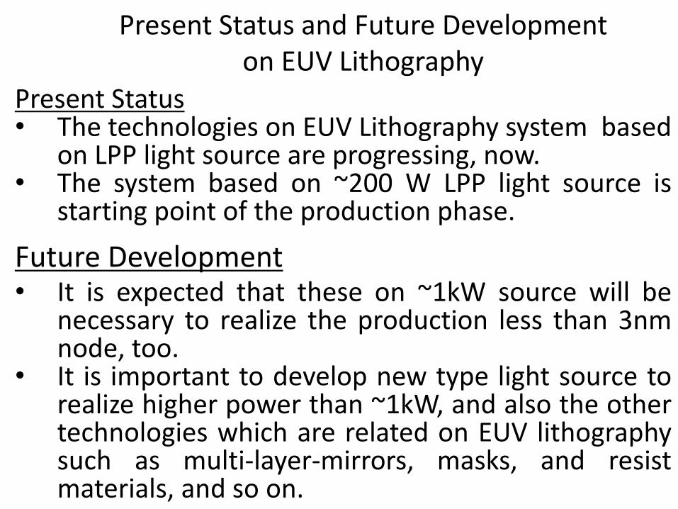
Present Status and Future Development on EUV Lithography
Present Status• The technologies on EUV Lithography system based
on LPP light source are progressing, now.• The system based on ~200 W LPP light source is
starting point of the production phase.
Future Development• It is expected that these on ~1kW source will be
necessary to realize the production less than 3nmnode, too.
• It is important to develop new type light source torealize higher power than ~1kW, and also the othertechnologies which are related on EUV lithographysuch as multi-layer-mirrors, masks, and resistmaterials, and so on.

Design study on high power EUV-FEL light source
Design concept
• High energy accelerator technologies bring us 10 kWclass high power EUV light source based on FreeElectron Laser (FEL).
Key technologies
• Super conducting accelerator technologies with EnergyRecovery Linac (ERL) (800MeV, 20 mA)
• High power FEL technologies (~30 kW)• Accelerator elements, systems and operation skill,
which are developed in cERL at KEK
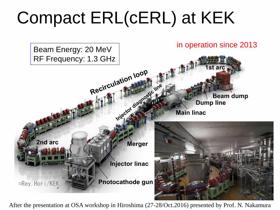
Compact ERL(cERL) at KEK
Beam Energy: 20 MeV
RF Frequency: 1.3 GHz
in operation since 2013
After the presentation at OSA workshop in Hiroshima (27-28/Oct.2016) presented by Prof. N. Nakamura

Prototype design of the EUV-FEL

FEL Performance
e-
<gb>=1561.1 st=48.5 fssp/p=0.299 %enx=1.98 mm·mradeny=0.71 mm·mrad
PFEL > 10 kW is achieved.
(PFEL=84 mJ x 162.5 MHz =13.7 kW, Iav=60pC x 162.5 MHz=9.75 mA)
FEL power without tapering: 12.9/25.8 kW @ 9.75/19.5 mA (162.5/325 MHz)
FEL power with 2% tapering: 14.4/28.8 kW @ 9.75/19.5 mA (162.5/325 MHz)
79.5 mJ
88.5mJ
<gb>=1561.1 st=48.5 fssp/p=0.299 %enx=1.98 mm·mradeny=0.71 mm·mrad
Energy spread is increased.
Courtesy of N. Nakamura

Our previous presentation on EUV-FEL9-11/Nov.2014: Workshop on EUV and Soft X-Ray Sources (Dublin)(Superconducting accelerator technology)
15-19/Jun./2015: EUVL Workshop (Hawaii) (Design of the total system)
6-7/July/2015: NGL Workshop (Tokyo) (in Japanese)9-11/Nov.2015 Workshop on EUV and Soft X-Ray Sources (Dublin)(Design of the total system ad superconducting technology)
13-16/Jun./2016: EUVL Workshop (Berkeley)(complete simulation result including the FEL production)
24-26/Oct./2016: EUVL Symposium (Hiroshima)(Complete design work and strategy to realize the system)
27-28/Oct./2016: OSA Workshop on Compact EUV & X-ray light sources (Hiroshima)
7-9/Nov. /2016: EUV Source Workshop (Amsterdam)(Strategy to realize the system)
13/Dec./2016: EUV-FEL Workshop (Tokyo)(Discussion with end users and tool venders and accelerator developer)
13-15/Jun./2017: EUVL Workshop (Berkeley) Now9

EUV-FEL Light Source Study Group for Industrialization
Industrialization of High Power EUV light
source based on ERL@KEK and FEL@QST
S. Ishihara (Leader)
H. Kawata et al.R. Hajima
T. KozawaH. KinoshitaM. Washio
N. Sei
I. MatsudaUniv. of Hyogo
Waseda Univ.Osaka Univ.
Utsunomiya Univ.T. Higashiguchi
KEK
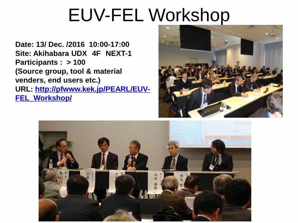
Date: 13/ Dec. /2016 10:00-17:00
Site: Akihabara UDX 4F NEXT-1
Participants : > 100
(Source group, tool & material
venders, end users etc.)
URL: http://pfwww.kek.jp/PEARL/EUV-
FEL_Workshop/
EUV-FEL Workshop

Time Title Speaker09:30 Start accepting10:00-10:10 Opening message Sunao Ishihara
(The U. of Tokyo)Keynote・Invited chairperson: Sunao Ishihara (The U. of Tokyo)10:10-12:0010:10-10:50 -Keynote-
”Neuromorphic Device for Cognitive Computing in the Big Data era”
Shintaro Yamamichi (IBM Japan)
10:50-11:25 -Invited-“Scaling of Semiconductor Integrated Circuits and EUV Lithography”
Hidemi Ishiuchi (EIDEC)
11:25-12:00 -Invited-"EUV Lithography Industrialization and future outlook"
Junji Miyazaki(ASML Japan)
- Lunch -【12:00-13:15】
EUV-FEL WORKSHOP : 2016.12.13 10:00-17:30 @AKIHABARA UDX 4F NEXT-1http://pfwww.kek.jp/PEARL/EUV-FEL_Workshop/presentaions.html
<Program>
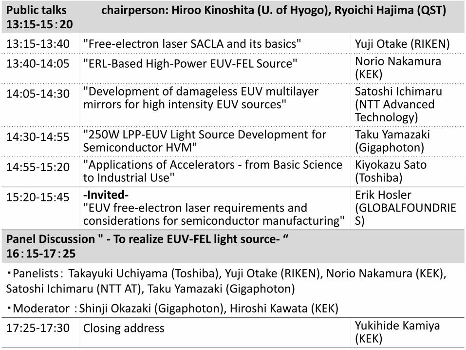
Public talks chairperson: Hiroo Kinoshita (U. of Hyogo), Ryoichi Hajima (QST)13:15-15:20
13:15-13:40 "Free-electron laser SACLA and its basics" Yuji Otake (RIKEN)
13:40-14:05 "ERL-Based High-Power EUV-FEL Source" Norio Nakamura (KEK)
14:05-14:30 "Development of damageless EUV multilayer mirrors for high intensity EUV sources"
Satoshi Ichimaru (NTT Advanced Technology)
14:30-14:55 "250W LPP-EUV Light Source Development for Semiconductor HVM"
Taku Yamazaki (Gigaphoton)
14:55-15:20 "Applications of Accelerators - from Basic Science to Industrial Use"
Kiyokazu Sato (Toshiba)
15:20-15:45 -Invited-"EUV free-electron laser requirements and considerations for semiconductor manufacturing"
Erik Hosler (GLOBALFOUNDRIES)
Panel Discussion " - To realize EUV-FEL light source- “ 16:15-17:25
・Panelists: Takayuki Uchiyama (Toshiba), Yuji Otake (RIKEN), Norio Nakamura (KEK), Satoshi Ichimaru (NTT AT), Taku Yamazaki (Gigaphoton)
・Moderator :Shinji Okazaki (Gigaphoton), Hiroshi Kawata (KEK)
17:25-17:30 Closing address Yukihide Kamiya (KEK)
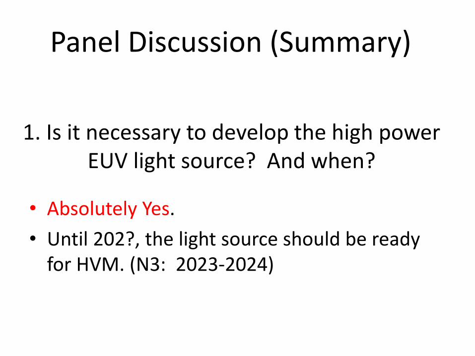
1. Is it necessary to develop the high power EUV light source? And when?
• Absolutely Yes.
• Until 202?, the light source should be ready for HVM. (N3: 2023-2024)
Panel Discussion (Summary)

2. What kinds of light source is possible? These feasibilities? (1)
• LPP: LPP will be a main player until 500W. – Present exposure system is designed to match the LPP light
source.– One of the big problem is the debris of Sn at the collector
mirror.
• ERL-FEL: It will be one of the promising player higher than 1kW.– The accelerator technologies of ERL have been partially
satisfied the requirement. – However, from the view point of industrialization, it is
necessary to develop the total system to realize the good quality of the beam at high current operation up to 10mA with a reasonable availability, and also size reduction.
– cERL gives us a very nice site for such development.
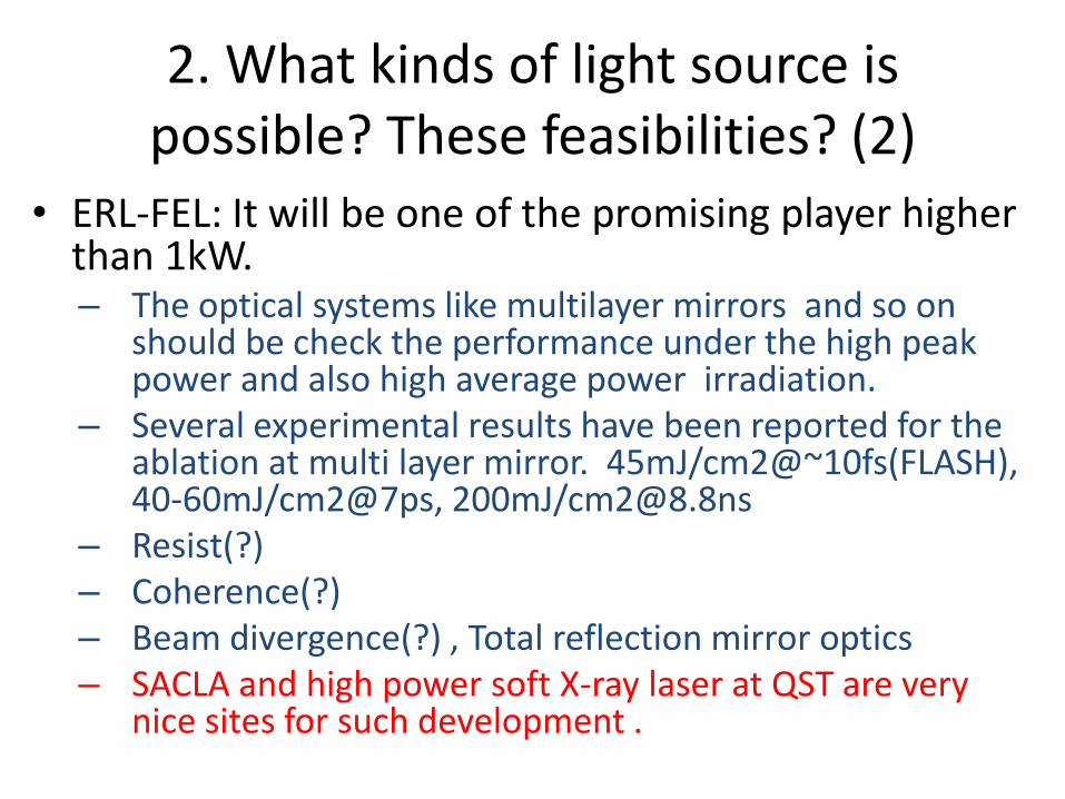
2. What kinds of light source is possible? These feasibilities? (2)
• ERL-FEL: It will be one of the promising player higher than 1kW.– The optical systems like multilayer mirrors and so on
should be check the performance under the high peak power and also high average power irradiation.
– Several experimental results have been reported for the ablation at multi layer mirror. 45mJ/cm2@~10fs(FLASH), 40-60mJ/cm2@7ps, 200mJ/[email protected]
– Resist(?)– Coherence(?)– Beam divergence(?) , Total reflection mirror optics– SACLA and high power soft X-ray laser at QST are very
nice sites for such development .

3. What kinds of R&D items for industrialization?
• It is necessary to develop the total system to realize the good quality of the beam at high current operation up to 10mA.– Brash up the accelerator components: super-
conduction cavity, electron gun, control systems and so on.
• Down size of the HVM ERL-FEL accelerator
• The optical systems like multilayer mirrors and so on should be checked the performance under the high peak power and also high average power irradiation.

4. What is necessary to realize the high power light source?
• Fundamental development should be done quickly and continuously.
• In order to push forward the progress, the coherent support messages from the related companies and communities are very important!
• The development should be done with the collaborative works between the related companies.

Challenge to upgrade the accelerator technologies

Availability Issues
• Electron gun
– Remote control of photocathode exchange
• SC Cavity
– Reduction of trip rate
– Pulse aging time for suppression of field emission increase
• Undulator
– Demagnetization of permanent magnets
• Cryoplant
– High pressure gas safety law reguration
– Safety inspection per year (in Japan)
Required availability for industrialization: ≥ 98 %( non operation time ≤ ~ 1 week per year)
Courtesy of N. Nakamura

VacuumSuitcase(Option)
Cathode Preparation System
Cathode Storage
Atomic H
Cathode Cleaning
NEA Activation
Cathode-container Loading
Cs
& O
2
Gun chamber
Cleaningchamber
Activationchamber
Storagechamber
Heating
Activate & storage 6~9 cathodes per day.
Short dead time for exchange cathode during gun operation.
Gatevalve
Courtesy of M. Yamamoto
22
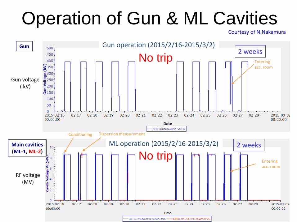
Operation of Gun & ML Cavities
Enteringacc. room
Gun voltage( kV)
Gun2 weeks
Main cavities(ML-1, ML-2)
RF voltage(MV)
2 weeks
Dispersion measurement
Enteringacc. room
in 2015
in 2015
Conditioning
Gun operation (2015/2/16-2015/3/2)
ML operation (2015/2/16-2015/3/2)
No trip
No trip
Courtesy of N.Nakamura
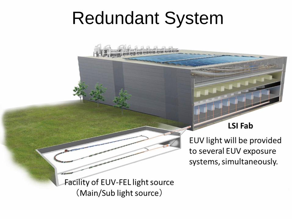
Redundant System
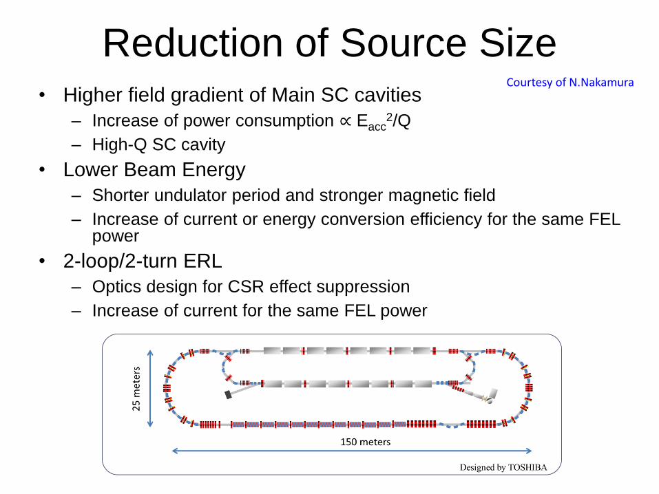
Reduction of Source Size• Higher field gradient of Main SC cavities
– Increase of power consumption ∝ Eacc2/Q
– High-Q SC cavity
• Lower Beam Energy
– Shorter undulator period and stronger magnetic field
– Increase of current or energy conversion efficiency for the same FEL power
• 2-loop/2-turn ERL
– Optics design for CSR effect suppression
– Increase of current for the same FEL power
Courtesy of N.Nakamura

SRF challenge: High-Q
State-of-the-art: LCLS-II CW cryomodule
KEK also tried N-doping using J-PARC furnace and obtained good results for single-cell cavity.
LCLS-II cryomodule pushing CW high-Q operation Nitrogen doped SRF cavity optimal Nb material and treatment magnetic shielding, magnetic hygiene,
demagnetize optimized cooling procedure
TTC meeting@MSU G. Wu
TTC meeting@MSU S.ChandrasekaranTTC meeting@KEKA. Melnychuk
Courtesy of K.Umemori

Staging to realize the EUV-FEL light source for Lithography
1. General understanding about EUV-FEL for Lithography– EUV-FEL Light source will be needed from the stage of 3nm Node (~2025).
– It is important to develop the feasible technologies on ERL-FEL and also handling of the high peak power FEL light source for EUV optical components ( multi-layer(ML) mirrors, photo resist materials, masks and so on)
2. Staging development processes
• 1st stage: Development of the feasible technologies– ERL-FEL: kW-class infrared FEL light will be demonstrated by using cERL
– Handling of high peak power EUV FEL light : Material developments on ML mirrors and so on by using low repetition FEL sources like SACLA and so on.
• 2nd stage: Development center of EUV-FEL system and lithography Phase 1: Establishment of the EUV-FEL system
– ERL-FEL: 10kW-class EUV FEL light will be produced by prototype ERL-FEL
– Handling of 10kW-class EUV FEL light: Interface optical systems to scanner and related materials will be established.
Phase 2: International Development Center of the EUV-FEL lithography
– Collaborative development of EUV-FEL lithography and related process between equipment venders and end users
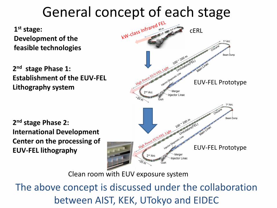
General concept of each stage
EUV-FEL Prototype
Clean room with EUV exposure system
1st stage: Development of the feasible technologies
2nd stage Phase 1: Establishment of the EUV-FEL Lithography system
2nd stage Phase 2: International Development Center on the processing of EUV-FEL lithography
cERL
The above concept is discussed under the collaboration between AIST, KEK, UTokyo and EIDEC
EUV-FEL Prototype

Summary
• Update of the EUV-FEL accelerator design is progressing from view points of end user demands.
• We organized EUV-FEL Workshop at last year and the R&D directions for accelerator technologies has been clarified; availability, size reduction, low operation cost, and so on.
• Staging procedure to the EUV-FEL light source for Lithography has been discussed with AIST, KEK, UTokyo, and EIDEC
EUV-FEL Design Group
(KEK) S. Chen, T. Furuya, K. Haga, I. Hanyu, K. Harada,
T. Honda, Y. Honda, E. Kako, Y. Kamiya, R. Kato,
H. Kawata, Y. Kobayashi, T. Konomi, T. Kubo,
S. Michizono, T. Miyajima, H. Nakai, N. Nakamura,
T. Obina, K. Oide, H. Sakai, M. Shimada, K. Tsuchiya,
K. Umemori, S. Yamaguchi, M. Yamamoto
(QST) R. Hajima
(Tohoku Unv.) N. Nishimori
The design study has been done under collaboration with a Japanese company.
Thank you for your attention!