stratix iii device handbook, volume 1. chapter 8. external...
TRANSCRIPT
© May 2009 Altera Corporation
SIII51008-1.8
8. External Memory Interfaces inStratix III Devices
IntroductionThe Stratix® III I/O structure has been completely redesigned to provide flexible, high-performance support for existing and emerging external memory standards. These include high-performance double data rate (DDR) memory standards such as DDR3, DDR2, DDR SDRAM, QDRII+, QDRII SRAM, and RLDRAM II.
Packed with features such as dynamic on-chip termination (OCT), trace mismatch compensation, read and write leveling, half data rate (HDR) blocks, and 4- to 36- bit programmable DQ group widths, Stratix III I/O elements provide easy-to-use built-in functionality required for a rapid and robust implementation.
Double data rate external memory support is found on all sides of the Stratix III FPGA. Stratix III devices provide an efficient architecture to quickly and easily fit wide external–memory interfaces with the new small modular I/O bank structure.
A self-calibrating megafunction (ALTMEMPHY) is optimized to take advantage of the Stratix III I/O structure, along with the new Quartus® II timing analysis tool, TimeQuest Timing Analyzer, which provides the total solution for the highest reliable frequency of operation across process, voltage, and temperature (PVT) variations.
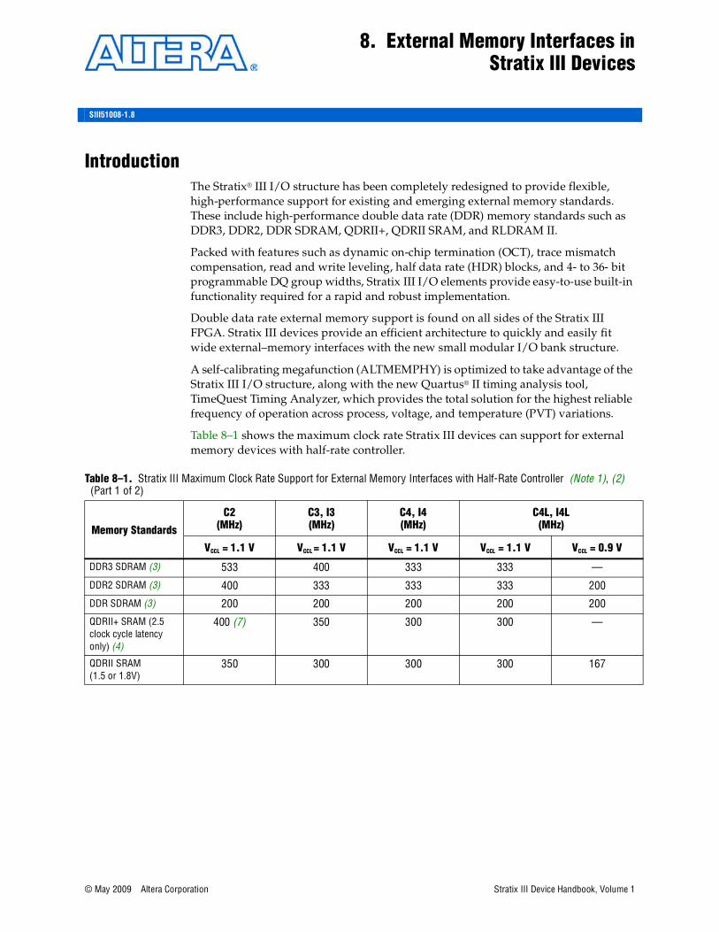
Table 8–1 shows the maximum clock rate Stratix III devices can support for external memory devices with half-rate controller.
Table 8–1. Stratix III Maximum Clock Rate Support for External Memory Interfaces with Half-Rate Controller (Note 1), (2) (Part 1 of 2)
Memory Standards
C2 (MHz)
C3, I3 (MHz)
C4, I4(MHz)
C4L, I4L(MHz)
VCCL = 1.1 V VCCL = 1.1 V VCCL = 1.1 V VCCL = 1.1 V VCCL = 0.9 V
DDR3 SDRAM (3) 533 400 333 333 —
DDR2 SDRAM (3) 400 333 333 333 200
DDR SDRAM (3) 200 200 200 200 200
QDRII+ SRAM (2.5 clock cycle latency only) (4)
400 (7) 350 300 300 —
QDRII SRAM (1.5 or 1.8V)
350 300 300 300 167
Stratix III Device Handbook, Volume 1

8–2 Chapter 8: External Memory Interfaces in Stratix III DevicesIntroduction
QDRII+ SRAM (×36 emulated mode) (2.5 clock cycle latency only) (4), (5), (6)
300 250 250 250 —
QDRII SRAM (×36 emulated mode)(1.5 V or 1.8 V) (5), (6)
300 250 250 250 —
RLDRAM II(1.5 or 1.8V)
400 333 300 300 —
Notes to Table 8–1:
(1) The supported operating frequencies listed here are memory interface maximums for the FPGA device family. Your design’s actual achievable performance is based on design- and system-specific factors, as well as static timing analysis of the completed design.
(2) With the exception for ×36 emulated mode, the values apply to column I/Os, row I/Os, and wraparound interface. Column I/Os refer to top and bottom I/Os, row I/Os refer to the left and right I/Os. Wraparound interface refers to interfaces with DQ/DQS groups wrapping over column I/Os and row I/Os of the device. The ×36 emulated mode values are for column I/Os and row I/Os.
(3) This performance specification applies for interfaces with single chip-select discrete components and single-rank unregistered modules. Refer to External Memory PHY Interface (ALTMEMPHY) Megafunction User Guide for a list of other supported configurations and corresponding performance specifications.
(4) The QDRII+SRAM devices with 2.0 clock cycle latency are not supported due to hardware limitations.(5) For more × 36 QDRII+/QDRII SRAM emulation mode information, refer to the “Combining ×16/×18 DQS/DQ groups for ×36 QDRII+/QDRII SRAM
Interface” on page 8–19.(6) The performance for ×36 emulated mode is lower than the performance for non ×36 emulated mode due to the double-loading of the CQ/CQn
pins. Double loading causes degradation in the signal slew rate which affects FPGA delay. Furthermore, due to the difference in slew rate, there is a shift in the setup and hold time window. You can perform an IBIS simulation to illustrate the shift in the clock signals.
(7) To achieve this data rate, Altera requires the QDRII+ SRAM device to have an echo clock tCQHCQ#H specification of 0.9ns or higher. QDRII+ devices with this specification are targeted for release later in 2009. In the interim, you can safely prototype with existing QDRII+ SRAM devices up to 375MHz.
Table 8–1. Stratix III Maximum Clock Rate Support for External Memory Interfaces with Half-Rate Controller (Note 1), (2) (Part 2 of 2)
Memory Standards
C2 (MHz)
C3, I3 (MHz)
C4, I4(MHz)
C4L, I4L(MHz)
VCCL = 1.1 V VCCL = 1.1 V VCCL = 1.1 V VCCL = 1.1 V VCCL = 0.9 V
Stratix III Device Handbook, Volume 1 © May 2009 Altera Corporation

Chapter 8: External Memory Interfaces in Stratix III Devices 8–3Introduction
Table 8–2 shows the maximum clock rate Stratix III devices can support for external memory devices with Full-Rate controller.
Table 8–2. Stratix III Maximum Clock Rate Support for External Memory Interfaces with Full-Rate Controller (Note 1), (2), (3), (4)
Memory Standards
C2(MHz)
C3, I3(MHz)
C4, I4(MHz)
C4L, I4L(MHz)
VCCL = 1.1 V VCCL = 1.1 V VCCL = 1.1 V VCCL = 1.1 V VCCL = 0.9 V
DDR2 SDRAM (5) 300 267 233 233 167
DDR SDRAM 200 200 200 200 167
Notes to Table 8–2:
(1) The supported operating frequencies listed here are memory interface maximums for the FPGA device family. Your design’s actual achievable performance is based on design and system-specific factors, as well as static timing analysis of the completed design.
(2) This performance specification applies for interfaces with single rank unregistered DIMMs and single chip-select discrete components. Refer to the External Memory PHY Interface (ALTMEMPHY) Megafunction User Guide for a list of other supported configurations and corresponding performance specifications.
(3) The values apply to column I/Os, rows I/Os and wraparound interface. Column I/Os refers to top and bottom I/Os. Row I/Os refers to left and right I/Os. Wrapwround interface refers to DQ/DQS groups wrapping over column I/Os and row I/Os of the device.
(4) It may be possible to close timing at up to 33MHz higher than stated above, depending on your design and the Quartus settings used. Refer to the section on advanced settings in the External Memory PHY Interface (ALTMEMPHY) Megafunction User Guide.
(5) We recommend the use of ALTMEMPHY AFI mode to achieve these quoted maximum clock rate due to lower performance of Non-AFI mode.
© May 2009 Altera Corporation Stratix III Device Handbook, Volume 1

8–4 Chapter 8: External Memory Interfaces in Stratix III DevicesIntroduction
Figure 8–1 shows a package bottom view for Stratix III external memory support, showing the phase-locked loop (PLL), delay-locked loop (DLL), and I/O banks. The number of available I/O banks and PLLs depend on the device density.
Figure 8–1. Stratix III Package Bottom View (Note 1), (2)
Notes to Figure 8–1:
(1) The number of I/O banks and PLLs available depends on the device density.(2) There is only one PLL in the center of each side of the device in EP3SL50, EP3SL70, and EP3SE50 devices.
DLL18A 8B 8C 7C 7B 7A
1A
1B
1C
2C
2B
2A
3A 3B 3C 4C 4B 4A
5A
5B
5C
6C
6B
6A
PLL_T1 PLL_T2
PLL_L2
PLL_L3
PLL_R2
PLL_R3
PLL_B2PLL_B1
PLL_L1
DLL4
PLL_R1
PLL_R4
DLL3
PLL_L4
DLL2
Stratix III Device
Stratix III Device Handbook, Volume 1 © May 2009 Altera Corporation

Chapter 8: External Memory Interfaces in Stratix III Devices 8–5Memory Interfaces Pin Support
Figure 8–2 shows an overview of the memory interface data path that uses all the Stratix III IOE features.
This chapter describes the hardware features in Stratix III devices that facilitate high-speed memory interfacing for each DDR memory standard. Stratix III devices feature DLLs, PLLs, dynamic OCT, read and write leveling, and deskew ciruitry.
Memory Interfaces Pin SupportA typical memory interface requires data (D, Q, or DQ), data strobe (DQS/CQ and DQSn/CQn), address, command, and clock pins. Some memory interfaces use data mask (DM) pins to enable write masking and QVLD pins to indicate that the read data is ready to be captured. This section describes how Stratix III devices support all these different pins.
f For more information on memory interfaces, refer to Stratix III Pin Connection Guidelines.
Figure 8–2. External Memory Interface Data Path Overview (Note 1), (2), (3)
Notes to Figure 8–2:(1) Each register block can be bypassed.(2) The blocks for each memory interface may differ slightly.(3) These signals may be bi-directional or uni-directional, depending on the memory standard. When bi-directional, the signal is active during both
read and write operations.
DDR OutputRegisters
MemoryStratix III FPGA
DLL
DDR Input Registers
Alignment & Synchronization
Registers
Half Data Rate Output Registers
Clock Management & Reset
4n 2nn
n
2n4n
FIFO(2)
DQ (Read)
DQ (Write)
DQS (Read)
Half Data Rate Input Registers
2n
DDR OutputRegisters
Half Data Rate Output Registers
4 2 DQS (Write)
Resynchronization Clock
Alignment Clock
DQS Write Clock
Half-RateResynchronization
Clock
Half-Rate Clock
AlignmentRegisters
AlignmentRegisters
2n
2
DQ Write Clock
PostambleControlCircuit
Postamble Enable
Postamble Clock
DQS EnableCircuit
DQS Logic Block
© May 2009 Altera Corporation Stratix III Device Handbook, Volume 1

8–6 Chapter 8: External Memory Interfaces in Stratix III DevicesMemory Interfaces Pin Support
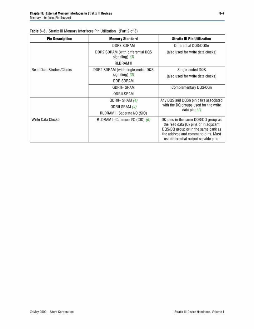
Data and Data-Strobe/Clock Pins Read data-strobes or clocks are called DQS pins. Depending on the memory specifications, DQS pins can be bi-directional single-ended signals (in DDR2 and DDR SDRAM), uni-directional differential signals (in RLDRAM II), bi-directional differential signals (DDR3 and DDR2 SDRAM), or uni-directional complementary signals (QDRII+ and QDRII SRAM). Connect the uni-directional read and write data-strobes or clocks to Stratix III DQS pins.
Stratix III devices offer differential input buffers for differential read data-strobe/clock operations and provide an independent DQS logic block for each CQn pin for complementary read data-strobe/clock operations. In the Stratix III pin tables (Table 8–3), the differential DQS pin-pairs are denoted as DQS and DQSn pins, while the complementary DQS signals are denoted as CQ and CQn pins. DQSn and CQn pins are marked separately in the pin table. Each CQn pin connects to a DQS logic block and the shifted CQn signals go to the negative-edge input registers in the IOE registers.
1 Use differential DQS signaling for DDR2 SDRAM interfaces running higher than 333 MHz.
1 For DDR3 and DDR2 SDRAM application, pseudo-differential DQS signaling is used for write operation.
Stratix III DDR memory interface data pins are called DQ pins. DQ pins can be bi-directional signals (in DDR3, DDR2, and DDR SDRAM, and RLDRAM II common I/O (CIO) interfaces), or uni-directional signals (in QDRII+, QDRII SRAM, and RLDRAM II separate I/O (SIO) devices). Connect the uni-directional read data signals to Stratix III DQ pins and the uni-directional write data signals to a different DQS/DQ group other than the read DQS/DQ group. The write clocks need to be assigned to the DQS/DQSn pins associated to this write DQS/DQ group. Do not use the CQ/CQn pin-pair for write clocks.
1 Using a DQS/DQ group for write data signals minimizes output skew, allows access to the write leveling circuitry (for DDR3 SDRAM interfaces), and allows for vertical migration. These pins also have access to deskewing circuitry that can compensate for delay mismatch between signals on the bus.
Table 8–3 summarizes the pin connections between a Stratix III device and an external memory device.
Table 8–3. Stratix III Memory Interfaces Pin Utilization (Part 1 of 3)
Pin Description Memory Standard Stratix III Pin Utilization
Read Data All DQ
Write Data All DQ (1)
Parity, DM, BWSn, NWSn, QVLD, ECC
All DQ (1), (2)
Stratix III Device Handbook, Volume 1 © May 2009 Altera Corporation
Chapter 8: External Memory Interfaces in Stratix III Devices 8–7Memory Interfaces Pin Support
Read Data Strobes/Clocks
DDR3 SDRAM
DDR2 SDRAM (with differential DQS signaling) (3)
RLDRAM II
Differential DQS/DQSn
(also used for write data clocks)
DDR2 SDRAM (with single-ended DQS signaling) (3)
DDR SDRAM
Single-ended DQS
(also used for write data clocks)
QDRII+ SRAM
QDRII SRAM
Complementary DQS/CQn
Write Data Clocks
QDRII+ SRAM (4)
QDRII SRAM (4)
RLDRAM II Seperate I/O (SIO)
Any DQS and DQSn pin pairs associated with the DQ groups used for the write
data pins(1)
RLDRAM II Common I/O (CIO) (6) DQ pins in the same DQS/DQ group as the read data (Q) pins or in adjacent
DQS/DQ group or in the same bank as the address and command pins. Must use differential output capable pins.
Table 8–3. Stratix III Memory Interfaces Pin Utilization (Part 2 of 3)
Pin Description Memory Standard Stratix III Pin Utilization
© May 2009 Altera Corporation Stratix III Device Handbook, Volume 1

8–8 Chapter 8: External Memory Interfaces in Stratix III DevicesMemory Interfaces Pin Support
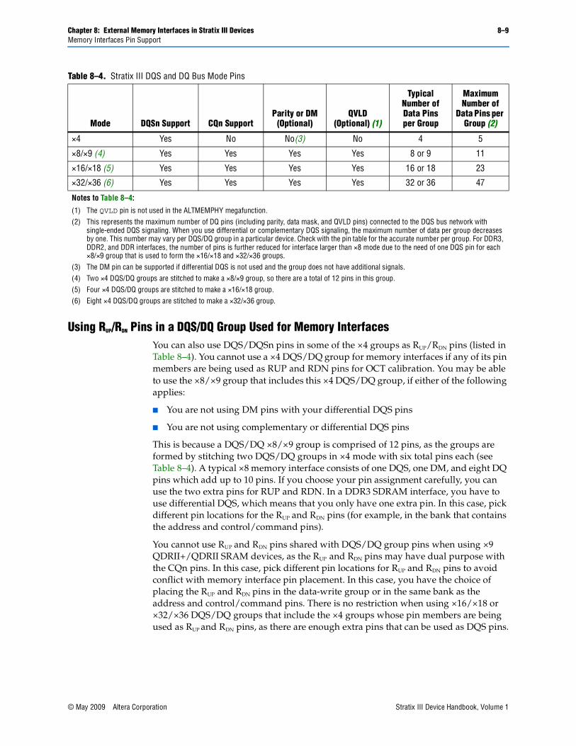
The DQS and DQ pin locations are fixed in the pin table. Memory interface circuitry is available in every Stratix III I/O bank. All memory interface pins support the I/O standards required to support DDR3, DDR2, DDR SDRAM, QDRII+, QDRII SRAM, and RLDRAM II devices.
The Stratix III device supports DQS and DQ signals with DQ bus modes of ×4, ×8/×9, ×16/×18, or ×32/×36, although not all devices support DQS bus mode ×32/×36. When any of these pins are not used for memory interfacing, you can use them as user I/Os. In addition, you can use any DQSn or CQn pins not used for clocking as DQ (data) pins. Table 8–4 lists pin support per DQS/DQ bus mode, including the DQS/CQ and DQSn/CQn pin pair.
Memory Clocks
(for addresses and commands) (5)
DDR3 SDRAM without levelingDDR2 SDRAM (with differential DQS
signaling)(3)
Any pins with DIFFIO_RX capability for the mem_clk[0] and mem_clk_n[0] signals
Any pins with DIFFOUT capability for the mem_clk[n:1] and
mem_clk_n[n:1] signals (where n is greater than or equal to 1)
DDR3 SDRAM with leveling Any unused DQ or DQS pins with DIFFIO_RX capability for the
mem_clk[0] and mem_clk_n[0] signals
Any unused DQ or DQS pins with DIFFOUT capability for the mem_clk[n:1] and
mem_clk_n[n:1] signals (where n is greater than or equal to 1)
DDR2 SDRAM (with single-ended DQS signaling) (3)
DDR SDRAM RLDRAM II
Any DIFFOUT pins
Notes to Table 8–3:
(1) If the write data signals are uni-directional, connect them, including the data mask pins, to a separate DQS/DQ group other than the read DQS/DQ group. Connect the write clock to the DQS and DQSn pin-pair associated with that DQS/DQ group. Do not use the CQ and CQn pin-pair as write clocks.
(2) The BWSn, NWSn, and DM pins need to be part of the write DQS/DQ group, while parity, QVLD, and ECC pins need to be part of the read DQS/DQ group.
(3) DDR2 SDRAM supports either single-ended or differential DQS signaling.(4) QDRII+/QDRII SRAM devices use K/K# clock pin-pairs to latch the write data, address, and control/command signals. The clocks must be part
of the DQS/DQ group and follow the write data clock rules in this case.(5) An ALTMEMPHY megafunction implementation for a DDR3, DDR2, or DDR SDRAM interface requires that you to place all memory clock
pin-pairs in a single DQ group of adequate width to minimize skew. For example, DIMMs requiring three memory clock pin-pairs need to use a ×4 DQS/DQ group.
(6) When interfacing with RLDRAM II 36 CIO devices, use two DQ pins in the 16/18 DQS/DQ groups that are DQS/DQSn pins in the 4 or 8/9 DQS/DQ groups for the write data clock.
Table 8–3. Stratix III Memory Interfaces Pin Utilization (Part 3 of 3)
Pin Description Memory Standard Stratix III Pin Utilization
Stratix III Device Handbook, Volume 1 © May 2009 Altera Corporation
Chapter 8: External Memory Interfaces in Stratix III Devices 8–9Memory Interfaces Pin Support
Using RUP/RDN Pins in a DQS/DQ Group Used for Memory InterfacesYou can also use DQS/DQSn pins in some of the ×4 groups as RUP/RDN pins (listed in Table 8–4). You cannot use a ×4 DQS/DQ group for memory interfaces if any of its pin members are being used as RUP and RDN pins for OCT calibration. You may be able to use the ×8/×9 group that includes this ×4 DQS/DQ group, if either of the following applies:
■ You are not using DM pins with your differential DQS pins
■ You are not using complementary or differential DQS pins
This is because a DQS/DQ ×8/×9 group is comprised of 12 pins, as the groups are formed by stitching two DQS/DQ groups in ×4 mode with six total pins each (see Table 8–4). A typical ×8 memory interface consists of one DQS, one DM, and eight DQ pins which add up to 10 pins. If you choose your pin assignment carefully, you can use the two extra pins for RUP and RDN. In a DDR3 SDRAM interface, you have to use differential DQS, which means that you only have one extra pin. In this case, pick different pin locations for the RUP and RDN pins (for example, in the bank that contains the address and control/command pins).
You cannot use RUP and RDN pins shared with DQS/DQ group pins when using ×9 QDRII+/QDRII SRAM devices, as the RUP and RDN pins may have dual purpose with the CQn pins. In this case, pick different pin locations for RUP and RDN pins to avoid conflict with memory interface pin placement. In this case, you have the choice of placing the RUP and RDN pins in the data-write group or in the same bank as the address and control/command pins. There is no restriction when using ×16/×18 or ×32/×36 DQS/DQ groups that include the ×4 groups whose pin members are being used as RUP and RDN pins, as there are enough extra pins that can be used as DQS pins.
Table 8–4. Stratix III DQS and DQ Bus Mode Pins
Mode DQSn Support CQn SupportParity or DM
(Optional)QVLD
(Optional) (1)
Typical Number ofData Pins per Group
Maximum Number of
Data Pins per Group (2)
×4 Yes No No(3) No 4 5
×8/×9 (4) Yes Yes Yes Yes 8 or 9 11
×16/×18 (5) Yes Yes Yes Yes 16 or 18 23
×32/×36 (6) Yes Yes Yes Yes 32 or 36 47
Notes to Table 8–4:
(1) The QVLD pin is not used in the ALTMEMPHY megafunction.(2) This represents the maximum number of DQ pins (including parity, data mask, and QVLD pins) connected to the DQS bus network with
single-ended DQS signaling. When you use differential or complementary DQS signaling, the maximum number of data per group decreases by one. This number may vary per DQS/DQ group in a particular device. Check with the pin table for the accurate number per group. For DDR3, DDR2, and DDR interfaces, the number of pins is further reduced for interface larger than ×8 mode due to the need of one DQS pin for each ×8/×9 group that is used to form the ×16/×18 and ×32/×36 groups.
(3) The DM pin can be supported if differential DQS is not used and the group does not have additional signals.(4) Two ×4 DQS/DQ groups are stitched to make a ×8/×9 group, so there are a total of 12 pins in this group. (5) Four ×4 DQS/DQ groups are stitched to make a ×16/×18 group. (6) Eight ×4 DQS/DQ groups are stitched to make a ×32/×36 group.
© May 2009 Altera Corporation Stratix III Device Handbook, Volume 1

8–10 Chapter 8: External Memory Interfaces in Stratix III DevicesMemory Interfaces Pin Support
You must pick your DQS and DQ pins manually for the ×8, ×16/×18, or ×32/×36 DQS/DQ group whose members are being used for RUP and RDN because the Quartus II software might not be able to place this correctly when there are no specific pin assignments and might give you a “no-fit” instead.
Table 8–5 shows the maximum number of DQS/DQ groups per side of the Stratix III device. For a more detailed listing of the number of DQS/DQ groups available per bank in each Stratix III device, see Figure 8–3 through Figure 8–7. These figures represent the package bottom view of the Stratix III device.
Table 8–5. Number of DQS/DQ Groups in Stratix III Devices per Side (Part 1 of 2)
Device Package Side ×4 (1) ×8/×9 ×16/×18 ×32/×36 (2)
EP3SE50EP3SL50EP3SL70
484-pin FineLine BGALeft/ Right 12 4 0 0
Top/ Bottom
5 2 0 0
780-pin FineLine BGALeft/ Right 14 6 2 0
Top/ Bottom
17 8 2 0
EP3SE80EP3SE110EP3SL110EP3SL150
780-pin FineLine BGALeft/ Right 14 6 2 0
Top/ Bottom
17 8 2 0
1152-pin FineLine BGALeft/ Right 26 12 4 0
Top/ Bottom
26 12 4 0
EP3SL200
780-pin Hybrid FineLine BGALeft/ Right 14 6 2 0
Top/ Bottom
17 8 2 0
1152-pin FineLine BGALeft/ Right 26 12 4 0
Top/ Bottom
26 12 4 0
1517-pin FineLine BGALeft/ Right 34 16 6 0
Top/ Bottom
38 18 8 4
EP3SE260
780-pin Hybrid FineLine BGALeft/ Right 14 6 2 0
Top/ Bottom
17 8 2 0
1152-pin FineLine BGALeft/ Right 26 12 4 0
Top/ Bottom
26 12 4 0
1517-pin FineLine BGALeft/ Right 34 16 6 0
Top/ Bottom
38 18 8 4
Stratix III Device Handbook, Volume 1 © May 2009 Altera Corporation

Chapter 8: External Memory Interfaces in Stratix III Devices 8–11Memory Interfaces Pin Support
EP3SL340
1152-pin Hybrid FineLine BGALeft/ Right 26 12 4 0
Top/ Bottom
26 12 4 0
1517-pin FineLine BGALeft/ Right 34 16 6 0
Top/ Bottom
38 18 8 4
1760-pin FineLine BGALeft/ Right 40 18 6 0
Top/ Bottom
44 22 10 4
Notes to Table 8–5:
(1) Some of the ×4 groups may use configuration or RUP/RDN pins. You cannot use these x4 groups if the pins are used for configuration or as RUP
and RDN pins for OCT calibration.(2) To interface with a ×36 QDRII+/QDRII SRAM device in a Stratix III FPGA that does not support the ×32/×36 DQS/DQ group, refer to the External
Memory PHY Interface (ALTMEMPHY) Megafunction User Guide.
Table 8–5. Number of DQS/DQ Groups in Stratix III Devices per Side (Part 2 of 2)
Device Package Side ×4 (1) ×8/×9 ×16/×18 ×32/×36 (2)
© May 2009 Altera Corporation Stratix III Device Handbook, Volume 1

8–12 Chapter 8: External Memory Interfaces in Stratix III DevicesMemory Interfaces Pin Support
Figure 8–3. Number of DQS/DQ Groups per Bank in EP3SE50, EP3SL50, and EP3SL70 Devices in the 484-pin FineLine BGA Package (Note 1)
Notes to Figure 8–3:
(1) This device does not support ×32/×36 mode.(2) You can also use DQS/DQSn pins in some of the ×4 groups as RUP/RDN pins. You cannot use a ×4 group for memory interfaces if two pins of the
group are being used as RUP and RDN pins for OCT calibration. You can still use the ×16/×18 or ×32/×36 groups that includes these ×4 groups. However, there are restrictions on using ×8/×9 groups that include these ×4 groups as described on page 8–9.
(3) Some of the DQS/DQ pins in this bank can also be used as configuration pins. Choose the DQS/DQ pins that are not going to be used by your configuration scheme.
(4) All I/O pin counts include eight dedicated clock inputs (CLK1p, CLK1n, CLK3p, CLK3n, CLK8p, CLK8n, CLK10p, and CLK10n)
DLL 1 DLL 4
I/O Bank 8C
24 User I/Osx4=2
x8/x9=1x16/x18=0
I/O Bank 7C
24 User I/Osx4=3
x8/x9=1x16/x18=0
I/O Bank 1A (2)
24 User I/Osx4=3
x8/x9=1x16/x18=0
I/O Bank 1C (3)
26 User I/Os (4)x4=3
x8/x9=1x16/x18=0
I/O Bank 2C
26 User I/Os (4)4=3
x8/x9=1x16/x18=0
I/O Bank 2A (2)
24 User I/Osx4=3
x8/x9=1x16/x18=0
DLL 2
I/O Bank 3C
24 User I/Osx4=2
x8/x9=1x16/x18=0
I/O Bank 4C
24 User I/Osx4=3
x8/x9=1x16/x18=0
DLL 3
I/O Bank 6A (2)
24 User I/Osx4=3
x8/x9=1x16/x18=0
I/O Bank 6C
26 User I/Os (4)x4=3
x8/x9=1x16/x18=0
I/O Bank 5C
26 User I/Os (4)x4=3
x8/x9=1x16/x18=0
I/O Bank 5A (2)
24 User I/Osx4=3
x8/x9=1x16/x18=0
EP3SE50, EP3SL50, and EP3SL70 Devices484-pin FineLine BGA
Stratix III Device Handbook, Volume 1 © May 2009 Altera Corporation

Chapter 8: External Memory Interfaces in Stratix III Devices 8–13Memory Interfaces Pin Support
Figure 8–4. Number of DQS/DQ Groups per Bank in EP3SE50, EP3SL50, EP3SL70, EP3SE80, EP3SE110, EP3SL110, EP3SL150, EP3SL200, and EP3SE260 Devices in the 780-pin FineLine BGA Package (Note 1)
Notes to Figure 8–4:(1) This device does not support ×32/×36 mode.(2) You can also use DQS/DQSn pins in some of the ×4 groups as RUP/RDN pins. You cannot use a ×4 group for memory interfaces if two pins of the
group are being used as RUP and RDN pins for OCT calibration. You can still use the ×16/×18 or ×32/×36 groups that includes these ×4 groups. However, there are restrictions on using ×8/×9 groups that include these ×4 groups as described on page 8–9.
(3) Some of the DQS/DQ pins in this bank can also be used as configuration pins. Choose the DQS/DQ pins that are not going to be used by your configuration scheme.
(4) All I/O pin counts include eight dedicated clock inputs (CLK1p, CLK1n, CLK3p, CLK3n, CLK8p, CLK8n, CLK10p, and CLK10n).
DLL 1 DLL 4
I/O Bank 8A (2)
40 User I/Osx4=6
x8/x9=3x16/x18=1
I/O Bank 8C
24 User I/Osx4=2
x8/x9=1x16/x18=0
I/O Bank 7C
24 User I/Osx4=3
x8/x9=1x16/x18=0
I/O Bank 7A (2)
40 User I/Osx4=6
x8/x9=3x16/x18=1
I/O Bank 1A (2)
32 User I/Osx4=4
x8/x9=2x16/x18=1
I/O Bank 1C (3)
26 User I/Os (4)x4=3
x8/x9=1x16/x18=0
I/O Bank 2C
26 User I/Os (4)x4=3
x8/x9=1x16x18=0
I/O Bank 2A (2)
32 User I/Osx4=4
x8/x9=2x16/x18=1
DLL 2
I/O Bank 3A (2)
40 User I/Osx4=6
x8/x9=3x16x18=1
I/O Bank 3C
24 User I/Osx4=2
x8/x9=1x16/x18=0
I/O Bank 4C
24 User I/Osx4=3
x8/x9=1x16x18=0
I/O Bank 4A (2)
40 User I/Osx4=6
x8x9=3x16x18=1
DLL 3
I/O Bank 6A (2)
32 User I/Osx4=4
x8/x9=2x16/x18=1
I/O Bank 6C
26 User I/Os (4)x4=3
x8/x9=1x16/x18=0
I/O Bank 5C
26 User I/Os (4)x4=3
x8x9=1x16x18=0
I/O Bank 5A
32 User I/Osx4=4
x8x9=2x16/x18=1
EP3SE50, EP3SL50, EP3SL70, EP3SE80, EP3SE110, EP3SL110, EP3SL150,EP3SL200, and EP3SE260 Devices
780-pin FineLine BGA
(2)
(2)
(2)
© May 2009 Altera Corporation Stratix III Device Handbook, Volume 1

8–14 Chapter 8: External Memory Interfaces in Stratix III DevicesMemory Interfaces Pin Support
Figure 8–5. Number of DQS/DQ Groups in EP3SE80, EP3SE110, EP3SL110, EP3SL150, EP3SL200, EP3SE260, and EP3SL340 Devices in the 1152-pin FineLine BGA Package (Note 1)
Notes to Figure 8–5:
(1) This device does not support ×32/×36 mode.(2) You can also use DQS/DQSn pins in some of the ×4 groups as RUP/RDN pins. You cannot use a ×4 group for memory interfaces if two pins of the
group are being used as RUP and RDN pins for OCT calibration. You can still use the ×16/×18 or ×32/×36 groups that includes these ×4 groups. However, there are restrictions on using ×8/×9 groups that include these ×4 groups as described on page 8–9.
(3) Some of the DQS/DQ pins in this bank can also be used as configuration pins. Choose the DQS/DQ pins that are not going to be used by your configuration scheme.
(4) All I/O pin counts include eight dedicated clock inputs (CLK1p, CLK1n, CLK3p, CLK3n, CLK8p, CLK8n, CLK10p, and CLK10n).
DLL1 DLL4
DLL2 DLL3
I/O Bank 8A (2)
40 User I/Osx4=6
x8/x9=3x16/x18=1
I/O Bank 8B
24 User I/Osx4=4
x8/x9=2x16/x18=1
I/O Bank 8C
32 User I/Osx4=3
x8/x9=1x16/x18=0
I/O Bank 7C
32 User I/Osx4=3
x8/x9=1x16/x18=0
I/O Bank 7B
24 User I/Osx4=4
x8/x9=2x16/x18=1
I/O Bank 7A (2)
40 User I/Osx4=6
x8/x9=3x16/x18=1
I/O Bank 6A (2)
48 User I/Osx4=7
x8/x9=3x16/x18=1
I/O Bank 6C
42 User I/Os (4)x4=6
x8/x9=3x16/x18=1
I/O Bank 5C
42 User I/Os (4)x4=6
x8/x9=3x16/x18=1
I/O Bank 5A (2)
48 User I/Osx4=7
x8/x9=3x16/x18=1
I/O Bank 4A (2)
40 User I/Osx4=6
x8/x9=3x16/x18=1
I/O Bank 4B24 User I/Os
x4=4x8/x9=2
x16/x18=1
I/O Bank 4C
32 User I/Osx4=3
x8/x9=1x16/x18=0
I/O Bank 3C
32 User I/Osx4=3
x8/x9=1x16/x18=0
I/O Bank 3B24 User I/Os
x4=4x8/x9=2
x16/x18=1
I/O Bank 3A (2)
40 User I/Osx4=6
x8/x9=3x16/x18=1
I/O Bank 2A (2)48 User I/Os
x4=7x8/x9=3
x16/x18=1
I/O Bank 2C42 User I/Os (4)
x4=6x8/x9=3
x16/x18=1
I/O Bank 1C (3)42 User I/Os (4)
x4=6x8/x9=3
x16/x18=1
I/O Bank 1A (2)
48 User I/Osx4=7
x8/x9=3x16/x18=1
EP3SE80, EP3SE110, EP3SL110, EP3SL150, EP3SL200, EP3SE260, and EP3SL340 Devices
1152-pin FineLine BGA
(2)
(2)
Stratix III Device Handbook, Volume 1 © May 2009 Altera Corporation

Chapter 8: External Memory Interfaces in Stratix III Devices 8–15Memory Interfaces Pin Support
Figure 8–6. Number of DQS/DQ Groups per Bank in EP3SL200, EP3SE260 and EP3SL340 Devices in the 1517-pin FineLine BGA Package
Notes to Figure 8–6:
(1) You can also use DQS/DQSn pins in some of the ×4 groups as RUP/RDN pins. You cannot use a ×4 group for memory interfaces if two pins of the group are being used as RUP and RDN pins for OCT calibration. You can still use the ×16/×18 or ×32/×36 groups that includes these ×4 groups. However, there are restrictions on using ×8/×9 groups that include these ×4 groups as described on page 8–9.
(2) Some of the DQS/DQ pins in this bank can also be used as configuration pins. Choose the DQS/DQ pins that are not going to be used by your configuration scheme.
(3) All I/O pin counts include eight dedicated clock inputs (CLK1p, CLK1n, CLK3p, CLK3n, CLK8p, CLK8n, CLK10p, and CLK10n) and eight dedicated corner PLL clock inputs (PLL_L1_CLKp, PLL_L1_CLKn, PLL_L4_CLKp, PLL_L4_CLKn, PLL_R4_CLKp, PLL_R4_CLKn, PLL_R1_CLKp, and PLL_R1_CLKn) that can be used for data inputs.
DLL1 DLL4
DLL2 DLL3
I/O Bank 8A (1)48 User I/Os
x4=8x8/x9=4
x16/x18=2x32/x36=1
I/O Bank 8B I/O Bank 8C I/O Bank 7C I/O Bank 7B I/O Bank 7A (1)
I/O Bank 6A (1)
I/O Bank 6B
I/O Bank 6C
I/O Bank 5C
I/O Bank 4A (1)I/O Bank 4BI/O Bank 4CI/O Bank 3CI/O Bank 3BI/O Bank 3A (1)
I/O Bank 2C
I/O Bank 1C (2)
I/O Bank 1B
I/O Bank 1A (1)
48 User I/Osx4=8
x8/x9=4x16/x18=2x32/x36=1
32 User I/Osx4=3
x8/x9=1x16/x18=0x32/x36=0
32 User I/Osx4=3
x8/x9=1x16/x18=0x32/x36=0
48 User I/Osx4=8
x8/x9=4x16/x18=2x32/x36=1
48 User I/Osx4=8
x8/x9=4x16/x18=2x32/x36=1
50 User I/Os (3)x4=7
x8/x9=3x16/x18=1x32/x36=0
24 User I/Osx4=4
x8/x9=2x16/x18=1x32/x36=0
42 User I/Os (3)x4=6
x8/x9=3x16/x18=1x32/x36=0
42 User I/Os (3)x4=6
x8/x9=3x16/x18=1x32/x36=0
48 User I/Osx4=8
x8/x9=4x16/x18=2x32/x36=1
48 User I/Osx4=8
x8/x9=4x16/x18=2x32/x36=1
32 User I/Osx4=3
x8/x9=1x16/x18=0x32/x36=0
32 User I/Osx4=3
x8/x9=1x16/x18=0x32/x36=0
48 User I/Osx4=8
x8/x9=4x16/x18=2x32/x36=1
48 User I/Osx4=8
x8/x9=4x16/x18=2x32/x36=1
50 User I/Os (3)x4=7
x8/x9=3x16/x18=1x32/x36=0
24 User I/Osx4=4
x8/x9=2x16/x18=1x32/x36=0
42 User I/Os (3)x4=6
x8/x9=3x16/x18=1x32/x36=0
42 User I/Os (3)x4=6
x8/x9=3x16/x18=1x32/x36=0
I/O Bank 5B
24 User I/Osx4=4
x8/x9=2x16/x18=1x32/x36=0
I/O Bank 5A (1)
50 User I/Os (3)x4=7
x8/x9=3x16/x18=1x32/x36=0
I/O Bank 2B
24 User I/Osx4=4
x8/x9=2x16/x18=1x32/x36=0
I/O Bank 2A (1)
50 User I/Os (3)x4=7
x8/x9=3x16/x18=1x32/x36=0
EP3SL200, EP3SE260, and EP3SL340 Devices1517-Pin FineLine BGA
(1)
(1)
© May 2009 Altera Corporation Stratix III Device Handbook, Volume 1
8–16 Chapter 8: External Memory Interfaces in Stratix III DevicesMemory Interfaces Pin Support
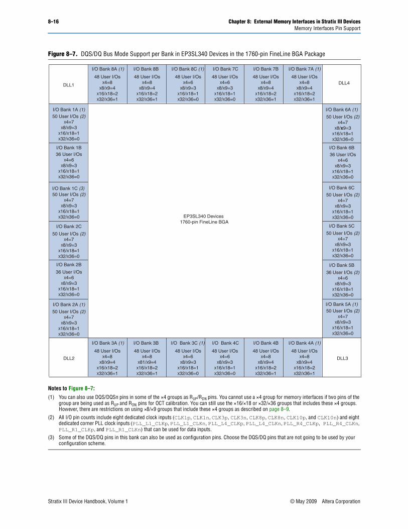
Figure 8–7. DQS/DQ Bus Mode Support per Bank in EP3SL340 Devices in the 1760-pin FineLine BGA Package
Notes to Figure 8–7:(1) You can also use DQS/DQSn pins in some of the ×4 groups as RUP/RDN pins. You cannot use a ×4 group for memory interfaces if two pins of the
group are being used as RUP and RDN pins for OCT calibration. You can still use the ×16/×18 or ×32/×36 groups that includes these ×4 groups. However, there are restrictions on using ×8/×9 groups that include these ×4 groups as described on page 8–9.
(2) All I/O pin counts include eight dedicated clock inputs (CLK1p, CLK1n, CLK3p, CLK3n, CLK8p, CLK8n, CLK10p, and CLK10n) and eight dedicated corner PLL clock inputs (PLL_L1_CLKp, PLL_L1_CLKn, PLL_L4_CLKp, PLL_L4_CLKn, PLL_R4_CLKp, PLL_R4_CLKn, PLL_R1_CLKp, and PLL_R1_CLKn) that can be used for data inputs.
(3) Some of the DQS/DQ pins in this bank can also be used as configuration pins. Choose the DQS/DQ pins that are not going to be used by your configuration scheme.
EP3SL340 Devices1760-pin FineLine BGA
DLL1 DLL4
DLL2 DLL3
I/O Bank 8A (1)
48 User I/Osx4=8
x8/x9=4x16/x18=2x32/x36=1
I/O Bank 8B I/O Bank 8C (1) I/O Bank 7C I/O Bank 7B I/O Bank 7A (1)
I/O Bank 6A (1)
I/O Bank 6B
I/O Bank 6C
I/O Bank 5C
I/O Bank 4A (1)I/O Bank 4BI/O Bank 4CI/O Bank 3C (1)I/O Bank 3BI/O Bank 3A (1)
I/O Bank 2C
I/O Bank 1C (3)
I/O Bank 1B
I/O Bank 1A (1)
I/O Bank 5B
I/O Bank 5A (1)
I/O Bank 2B
I/O Bank 2A (1)
48 User I/Osx4=8
x8/x9=4x16/x18=2x32/x36=1
48 User I/Osx4=6
x8/x9=3x16/x18=1x32/x36=0
48 User I/Osx4=6
x8/x9=3x16/x18=1x32/x36=0
48 User I/Osx4=8
x8/x9=4x16/x18=2x32/x36=1
48 User I/Osx4=8
x8/x9=4x16/x18=2x32/x36=1
50 User I/Os (2)x4=7
x8/x9=3x16/x18=1x32/x36=0
36 User I/Osx4=6
x8/x9=3x16/x18=1x32/x36=0
50 User I/Os (2)x4=7
x8/x9=3x16/x18=1x32/x36=0
50 User I/Os (2)x4=7
x8/x9=3x16/x18=1x32/x36=0
36 User I/Os (2)x4=6
x8/x9=3x16/x18=1x32/x36=0
50 User I/Os (2)x4=7
x8/x9=3x16/x18=1x32/x36=0
48 User I/Osx4=8
x8/x9=4x16/x18=2x32/x36=1
48 User I/Osx4=8
x8/x9=4x16/x18=2x32/x36=1
48 User I/Osx4=6
x8/x9=3x16/x18=1x32/x36=0
48 User I/Osx4=6
x8/x9=3x16/x18=1x32/x36=0
48 User I/Osx4=8
x81/x9=4x16/x18=2x32/x36=1
48 User I/Osx4=8
x8/x9=4x16/x18=2x32/x36=1
50 User I/Os (2)x4=7
x8/x9=3x16/x18=1x32/x36=0
36 User I/Osx4=6
x8/x9=3x16/x18=1x32/x36=0
50 User I/Os (2)x4=7
x8/x9=3x16/x18=1x32/x36=0
50 User I/Os (2)x4=7
x8/x9=3x16/x18=1x32/x36=0
36 User I/Osx4=6
x8/x9=3x16/x18=1x32/x36=0
50 User I/Os (2)x4=7
x8/x9=3x16/x18=1x32/x36=0
Stratix III Device Handbook, Volume 1 © May 2009 Altera Corporation

Chapter 8: External Memory Interfaces in Stratix III Devices 8–17Memory Interfaces Pin Support
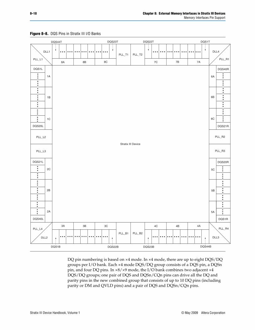
The DQS and DQSn pins are listed in the Stratix III pin tables asDQSXY and DQSnXY, respectively, where X denotes the DQS/DQ grouping number, and Y denotes whether the group is located on the top (T), bottom (B), left (L), or right (R) side of the device.
The corresponding DQ pins are marked as DQXY, where X indicates which DQS group the pins belong to and Y indicates whether the group is located on the top (T), bottom (B), left (L), or right (R) side of the device. For example, DQS1L indicates a DQS pin, located on the left side of the device. See Figure 8–8 for illustrations. The DQ pins belonging to that group are shown as DQ1L in the pin table.
The numbering scheme starts from the top-left side of the device going counter-clockwise. Figure 8–8 shows how the DQS/DQ groups are numbered in a package bottom view of the device. The top and bottom sides of the device can contain up to 44 ×4 DQS/DQ groups. The left and right sides of the device can contain up to 40 ×4 DQS/DQ groups.
The parity, DM, BWSn, NWSn, ECC, and QVLD pins are shown as DQ pins in the pin table. When not used as memory interface pins, these pins are available as regular I/O pins.
© May 2009 Altera Corporation Stratix III Device Handbook, Volume 1
8–18 Chapter 8: External Memory Interfaces in Stratix III DevicesMemory Interfaces Pin Support
DQ pin numbering is based on ×4 mode. In ×4 mode, there are up to eight DQS/DQ groups per I/O bank. Each ×4 mode DQS/DQ group consists of a DQS pin, a DQSn pin, and four DQ pins. In ×8/×9 mode, the I/O bank combines two adjacent ×4 DQS/DQ groups; one pair of DQS and DQSn/CQn pins can drive all the DQ and parity pins in the new combined group that consists of up to 10 DQ pins (including parity or DM and QVLD pins) and a pair of DQS and DQSn/CQn pins.
Figure 8–8. DQS Pins in Stratix III I/O Banks
DLL1
8A 8B 8C 7C 7B 7A
DQS44T
DQS1L
1A
1B
1C
2C
2B
2A
DQS40L
3A 3B 3C 4C 4B 4A
5A
5B
5C
6C
6B
6A
PLL_T1 PLL_T2
PLL_L2
PLL_L3
PLL_R2
PLL_R3
PLL_B2PLL_B1
DQS20L
PLL_L1
DQS23T DQS22T DQS1T
DQS40R
DQS21R
DQS1R
DQS1B DQS22B DQS23B DQS44B
DQS20RDQS21L
DLL4
PLL_R1
PLL_R4
DLL3
PLL_L4
DLL2
Stratix III Device
Stratix III Device Handbook, Volume 1 © May 2009 Altera Corporation

Chapter 8: External Memory Interfaces in Stratix III Devices 8–19Memory Interfaces Pin Support
Similarly, in ×16/×18 mode, the I/O bank combines four adjacent ×4 DQS/DQ groups to create a group with a maximum of 19 DQ pins (including parity or DM and QVLD pins) and a pair of DQS/CQ and DQSn/CQn pins. In ×32/×36 mode, the I/O bank combines eight adjacent ×4 DQS DQ groups together to create a group with a maximum of 37 DQ pins (including parity or DM and QVLD pins) and a pair of DQS/CQ and DQSn/CQn pins.
Stratix III modular I/O banks allow easy formation of the DQS/DQ groups. If all the pins in the I/O banks are user I/O pins and are not used for programming, RUP/RDN used for OCT calibration, or PLL clock output pins, you can divide the number of I/O pins in the bank by six to get the maximum possible number of ×4 groups. You can then divide that number by two, four, or eight to get the maximum possible number of ×8/×9, ×16/×18, or ×32/×36, respectively (see Table 8–6). However, some of the pins in the I/O bank may be used for other functions.
Combining ×16/×18 DQS/DQ groups for ×36 QDRII+/QDRII SRAM InterfaceThis implementation combines two ×16/×18 DQS/DQ groups to interface with a ×36 QDRII+/QDRII SRAM device. The ×36 read data bus uses two ×16/×18 groups, while the ×36 write data uses another two ×16/×18 groups or four ×8/×9 groups. The CQ/CQn signal traces are split on the board trace to connect two pairs of DQS/CQn pins in the FPGA. This is the only connection on the board that you need to change for this implementation. Other QDRII+/QDRII SRAM interface rules for Stratix III devices also apply for this implementation.
1 Altera’s ALTMEMPHY megafunction does not use the QVLD signal, so you can leave the QVLD signal unconnected as in any QDRII+/QDRII SRAM interfaces in the Stratix III devices.
f For more information about the ALTMEMPHY megafunction, refer to the ALTMEMPHY Megafunction User Guide.
Rules to Combine GroupsIn 780- and 1152-pin package devices, there is at most one ×16/×18 group per I/O sub-bank. You can combine ×16/×18 groups from a single side of the device for a x36 interface. For devices that do not have four ×16/×18 groups in a single side of the device to form two ×36 groups for read and write data, you can form one ×36 group on one side of the device, and another ×36 group on the other side of the device. For
Table 8–6. DQ/DQS Group in Stratix III Modular I/O Banks
Modular I/O Bank Size
Maximum Possible Number of
×4 Groups (1)
Maximum Possible Number of ×8/×9
Groups
Maximum Possible Number of ×16/×18
Groups
Maximum Possible Number of ×32/×36
Groups
24 pins 4 2 1 0
32 pins 5 2 1 0
40 pins 6 3 1 0
48 pins 8 4 2 1
Note to Table 8–6:(1) Some of the ×4 groups may use RUP/RDN pins. You cannot use these groups if you use the Stratix III calibrated OCT feature, as described in
page 8–9.
© May 2009 Altera Corporation Stratix III Device Handbook, Volume 1
8–20 Chapter 8: External Memory Interfaces in Stratix III DevicesMemory Interfaces Pin Support
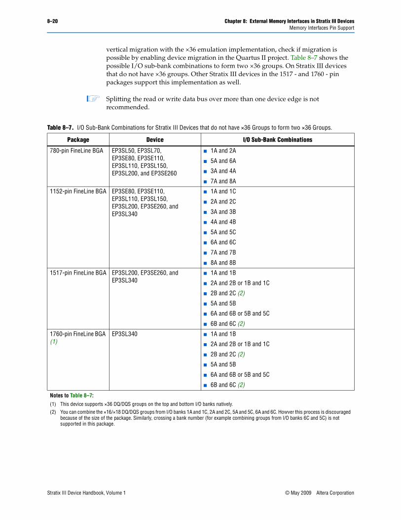
vertical migration with the ×36 emulation implementation, check if migration is possible by enabling device migration in the Quartus II project. Table 8–7 shows the possible I/O sub-bank combinations to form two ×36 groups. On Stratix III devices that do not have ×36 groups. Other Stratix III devices in the 1517 - and 1760 - pin packages support this implementation as well.
1 Splitting the read or write data bus over more than one device edge is not recommended.
Table 8–7. I/O Sub-Bank Combinations for Stratix III Devices that do not have ×36 Groups to form two ×36 Groups.
Package Device I/O Sub-Bank Combinations
780-pin FineLine BGA EP3SL50, EP3SL70,EP3SE80, EP3SE110,EP3SL110, EP3SL150,EP3SL200, and EP3SE260
■ 1A and 2A
■ 5A and 6A
■ 3A and 4A
■ 7A and 8A
1152-pin FineLine BGA EP3SE80, EP3SE110, EP3SL110, EP3SL150,EP3SL200, EP3SE260, andEP3SL340
■ 1A and 1C
■ 2A and 2C
■ 3A and 3B
■ 4A and 4B
■ 5A and 5C
■ 6A and 6C
■ 7A and 7B
■ 8A and 8B
1517-pin FineLine BGA EP3SL200, EP3SE260, and EP3SL340
■ 1A and 1B
■ 2A and 2B or 1B and 1C
■ 2B and 2C (2)
■ 5A and 5B
■ 6A and 6B or 5B and 5C
■ 6B and 6C (2)
1760-pin FineLine BGA (1)
EP3SL340 ■ 1A and 1B
■ 2A and 2B or 1B and 1C
■ 2B and 2C (2)
■ 5A and 5B
■ 6A and 6B or 5B and 5C
■ 6B and 6C (2)
Notes to Table 8–7:(1) This device supports ×36 DQ/DQS groups on the top and bottom I/O banks natively.(2) You can combine the ×16/×18 DQ/DQS groups from I/O banks 1A and 1C, 2A and 2C, 5A and 5C, 6A and 6C. Howver this process is discouraged
because of the size of the package. Similarly, crossing a bank number (for example combining groups from I/O banks 6C and 5C) is not supported in this package.
Stratix III Device Handbook, Volume 1 © May 2009 Altera Corporation

Chapter 8: External Memory Interfaces in Stratix III Devices 8–21Memory Interfaces Pin Support
Optional Parity, DM, BWSn, NWSn, ECC and QVLD PinsIn Stratix III devices, you can use any of the DQ pins from the same DQS/DQ group for data as parity pins. The Stratix III device family supports parity in ×8/×9, ×16/×18, and ×32/×36 modes. There is one parity bit available per eight bits of data pins. Use any of the DQ (or D) pins in the same DQS/DQ group as data for parity as they are treated, configured, and generated like a DQ pin.
DM pins are only required when writing to DDR3, DDR2, DDR SDRAM, and RLDRAM II devices. QDRII+ and QDRII SRAM devices use the BWSn (or NWSn in the ×8 QDRII SRAM devices) signal to select which byte to write into the memory. Each group of DQS and DQ signals in DDR3, DDR2, and DDR SDRAM devices require a DM pin. There is one DM pin per RLDRAM II device and one BWSn pin per 9 bits of data in ×9, ×18, and ×36 QDRII+/QDRII SRAM. The ×8 QDRII SRAM device has two BWSn pins per 8 data bits, which are referred to as NWSn pins.
A low signal on DM, NWSn, or BWSn indicates that the write is valid. If the DM/BWSn/NWSn signal is high, the memory masks the DQ signals. If the system does not require write data masking, connect the memory DM pins low to indicate every write data is valid. You can use any of the DQ pins in the same DQS/DQ group as write data for the DM/BWSn/NWSn signals. Generate the DM or BWSn signals using DQ pins and configure the signals similar to the DQ (or D) output signals. Stratix III devices do not support the DM signal in ×4 DDR3 SDRAM or in ×4 DDR2 SDRAM interfaces with differential DQS signaling.
Some DDR3, DDR2, and DDR SDRAM devices or modules support error correction coding (ECC), which is a method of detecting and automatically correcting errors in data transmission. In a 72-bit DDR3, DDR2, or DDR SDRAM interface, typically eight ECC pins are used in addition to the 64 data pins. Connect the DDR3, DDR2, and DDR SDRAM ECC pins to a Stratix III device DQS/DQ group. These signals are also generated similar to DQ pins. The memory controller needs encoding and decoding logic for ECC data. You can also use the extra byte of data for other error checking methods.
QVLD pins are used in RLDRAM II and QDRII+ SRAM interfaces to indicate read data availability. There is one QVLD pin per memory device. A high on QVLD indicates that the memory is outputting the data requested. Similar to DQ inputs, this signal is edge-aligned with the read clock signals (CQ/CQn in QDRII+/QDRII SRAM and QK/QK# in RLDRAM II) and is sent half a clock cycle before data starts coming out of the memory. The QVLD pin is not used in the ALTMEMPHY megafunction solution for QDRII+ SRAM.
For more information about the parity, ECC, and QVLD pins as these pins are treated as DQ pins refer to “Data and Data-Strobe/Clock Pins” on page 8–6.
Address and Control/Command Pins Address and control/command signals are typically sent at single data rate. The only exception is in QDRII SRAM burst-of-two devices, where the read address needs to be captured on the rising edge of the clock while the write address needs to be captured on the falling edge of the clock by the memory. There is no special circuitry required for the address and control/command pins. You can use any of the user I/O pins in the same I/O bank as the data pins.
© May 2009 Altera Corporation Stratix III Device Handbook, Volume 1

8–22 Chapter 8: External Memory Interfaces in Stratix III DevicesStratix III External Memory Interface Features
Memory Clock PinsIn addition to DQS (and CQn) signals to capture data, DDR3, DDR2, DDR SDRAM, and RLDRAM II use an extra pair of clocks, called CK and CK# signals, to capture the address and control/command signals. The CK/CK# signals need to be generated to mimic the write data-strobe using Stratix III DDR I/O registers (DDIOs) to ensure that timing relationships between the CK/CK# and DQS signals (tDQSS in DDR3, DDR2, and DDR SDRAM or tCKDK in RLDRAM II) are met. QDRII+ and QDRII SRAM devices use the same clock (K/K#) to capture data, address, and control/command signals.
Memory clock pins in Stratix III devices are generated using a DDIO register going to differential output pins, marked in the pin table with DIFFOUT, DIFFIO_TX, and DIFFIO_RX prefixes. For more information about which pins to use for memory clock pins, refer to Table 8–3 on page 8–6.
Figure 8–9 shows the memory clock generation block diagram for Stratix III devices.
Stratix III External Memory Interface FeaturesStratix III devices are rich with features that allow robust high-performance external memory interfacing. The ALTMEMPHY megafunction allows you to set these external memory interface features and helps set up the physical interface (PHY) best suited for your system. This section describes each Stratix III device feature that is used in external memory interfaces from the DQS phase-shift circuitry, DQS logic block, leveling multiplexers, dynamic OCT control block, IOE registers, IOE features, and PLL.
Figure 8–9. Memory Clock Generation Block Diagram (Note 1), (2)
Notes to Figure 8–9:
(1) Refer to Table 8–3 for pin location requirements for these pins.(2) The mem_clk[0] and mem_clk_n[0] pins for DDR3, DDR2, and DDR SDRAM interfaces uses the I/O input buffer for feedback, therefore,
bi-directional I/O buffers are used for these pins. For memory interfaces using a differential DQS input, the input feedback buffer is configured as differential input; for memory interfaces using a single-ended DQS input, the input buffer is configured as a single-ended input. Using a single-ended input feedback buffer requires that I/O standard’s VREF voltage is provided to that I/O bank’s VREF pins.
CK or DK or K (2)
QD
QD
System Clock
FPGA LEs I/O Elements
VCC
CK# or DK# or K# (2)
Stratix III Device Handbook, Volume 1 © May 2009 Altera Corporation

Chapter 8: External Memory Interfaces in Stratix III Devices 8–23Stratix III External Memory Interface Features
1 When using the Altera memory controller MegaCore® functions, the PHY is instantiated for you.
1 The ALTMEMPHY megafunction and the Altera memory controller MegaCore functions can run at half the frequency of the I/O interface of the memory devices to allow better timing management in high-speed memory interfaces. Stratix III devices have built-in registers to convert data from full-rate(I/O frequency) to half-rate (controller frequency) and vice versa. You can bypass these registers if your memory controller is not running at half the rate of the I/O frequency.
DQS Phase-Shift CircuitryStratix III phase-shift circuitry provides phase shift to the DQS and CQn pins on read transactions, when the DQS/CQ and CQn pins are acting as input clocks or strobes to the FPGA. DQS phase-shift circuitry consists of DLLs that are shared between multiple DQS pins and the phase-offset module to further fine-tune the DQS phase shift for different sides of the device. Figure 8–10 shows how the DQS phase-shift circuitry is connected to the DQS/CQ and CQn pins in the device.
© May 2009 Altera Corporation Stratix III Device Handbook, Volume 1

8–24 Chapter 8: External Memory Interfaces in Stratix III DevicesStratix III External Memory Interface Features
DQS phase-shift circuitry is connected to the DQS logic blocks that control each DQS/CQ or CQn pin. The DQS logic blocks allow the DQS delay settings to be updated concurrently at every DQS/CQ or CQn pin.
Figure 8–10. DQS and CQn Pins and DQS Phase-Shift Circuitry (Note 1)
Notes to Figure 8–10:
(1) Refer to“DLL” on page 8–25 for possible reference input clock pins for each DLL.(2) You can configure each DQS/CQn signal pair with a phase shift based on one of two possible DLL output settings.
DLLReferenceClock (2)
DQSPhase-Shift
Circuitry
DQS/CQPin
CQnPin
CQnPin
DQS/CQPin
to IOE
%t
%t
%t
%t
DQSPhase-Shift
Circuitry
DLLReferenceClock (2)
DLLReferenceClock (2)
DQS/CQPin
CQnPin
DQS/CQPin
CQnPin
to IOE to IOE to IOE
%t%t %t
to IOE
%t
DQS LogicBlocks
DQS/CQPin
CQnPin
CQnPin
DQS/CQPin
to IOE to IOEto IOEto IOE
%t%t%t%t
DQS/CQPin
CQnPin
DQS/CQPin
CQnPin
%t
%t
%t
%t
DQS LogicBlocks
DLLReferenceClock (2)
DQSPhase-Shift
Circuitry
to IOE
to IOE
to IOE
DQSPhase-Shift
Circuitry
to IOE
to IOE
to IOE
to IOE
Stratix III Device Handbook, Volume 1 © May 2009 Altera Corporation

Chapter 8: External Memory Interfaces in Stratix III Devices 8–25Stratix III External Memory Interface Features
DLLDQS phase-shift circuitry uses a DLL to dynamically measure the clock period needed by the DQS/CQ and CQn pin. The DLL, in turn, uses a frequency reference to dynamically generate control signals for the delay chains in each of the DQS and CQn pins, allowing it to compensate for PVT variations. The DQS delay settings are Gray-coded to reduce jitter when the DLL updates the settings. Phase-shift circuitry needs a maximum of 1280 clock cycles to calculate the correct input clock period. Do not send data during these clock cycles since there is no guarantee it will be properly captured. As the settings from the DLL may not be stable until this lock period has elapsed, you should be aware that anything using these settings (including the leveling delay system) may be unstable during this period.
1 Use the DQS phase-shift circuitry for any memory interfaces that are less than 100 MHz. The DQS signal is shifted by 2.5 ns. Even if the DQS signal is not shifted exactly to the middle of the DQ valid window, the I/O element should still be able to capture the data in low frequency applications where a large amount of timing margin is available.
There are four DLLs in a Stratix III device, located in each corner of the device. These DLLs support a maximum of four unique frequencies, with each DLL running at one frequency. Each DLL can have two outputs with different phase offsets, which allow one Stratix III device to have eight different DLL phase shift settings. Figure 8–11 shows the DLL and I/O bank locations in Stratix III devices from a package bottom view.
© May 2009 Altera Corporation Stratix III Device Handbook, Volume 1

8–26 Chapter 8: External Memory Interfaces in Stratix III DevicesStratix III External Memory Interface Features
The DLL can access the two adjacent sides from its location within the device. For example, DLL 1 on the top left of the device can access the top side (I/O banks 7A, 7B, 7C, 8A, 8B, and 8C) and the left side of the device (I/O banks 1A, 1B, 1C, 2A, 2B, and 2C). This means that each I/O bank is accessible by two DLLs, giving more flexibility to create multiple frequencies and multiple-type interfaces. For example, you can design an interface spanning one side of the device or within two sides adjacent to the DLL. The DLL outputs the same DQS delay settings for both sides of the device adjacent to the DLL.
Each bank can use settings from either or both DLLs that the bank is adjacent to. For example, DQS1L can get its phase-shift settings from DLL1, while DQS2L can get its phase-shift settings from DLL2. Table 8–8 lists the DLL location and supported I/O banks for Stratix III devices.
Figure 8–11. Stratix III DLL and I/O Bank Locations (Package Bottom View)
PLL_T1 PLL_T2
PLL_B1 PLL_B2
Stratix III FPGA
8A 8B 8C 7C 7B 7A
3A 3B 3C 4C 4B 4A
2A
2B
2C
PLL_L3
PLL_L2
1C
1B
1A
PLL_R3
PLL_R2
5A
5B
5C
6C
6B
6A
66
6
6
6
6
6
6
DLL1
PLL_L1
DLL4
PLL_R1
DLL3
PLL_R4
DLL2
PLL_L4
Stratix III Device Handbook, Volume 1 © May 2009 Altera Corporation
Chapter 8: External Memory Interfaces in Stratix III Devices 8–27Stratix III External Memory Interface Features
1 You can only have one memory interface in each I/O sub-bank (such as I/O sub-banks 1A, 1B, and 1C) when you use leveling delay chains. This is because there is only one leveling delay chain per I/O sub-bank.
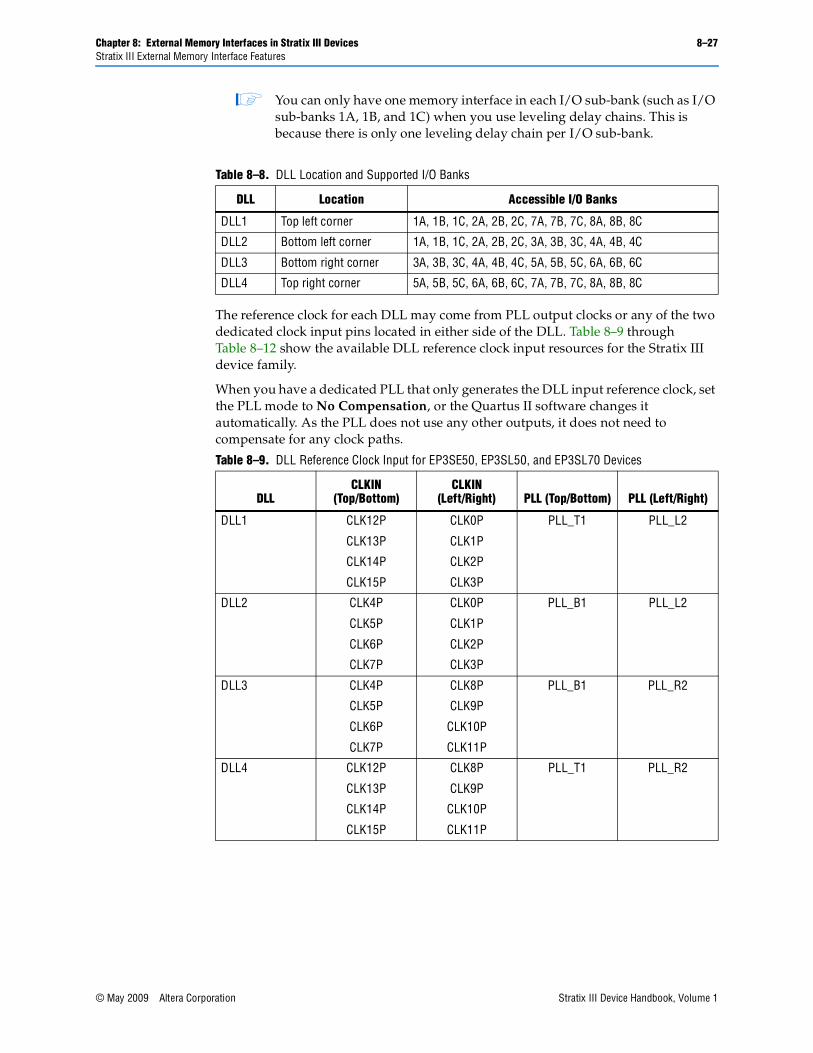
The reference clock for each DLL may come from PLL output clocks or any of the two dedicated clock input pins located in either side of the DLL. Table 8–9 through Table 8–12 show the available DLL reference clock input resources for the Stratix III device family.
When you have a dedicated PLL that only generates the DLL input reference clock, set the PLL mode to No Compensation, or the Quartus II software changes it automatically. As the PLL does not use any other outputs, it does not need to compensate for any clock paths.
Table 8–8. DLL Location and Supported I/O Banks
DLL Location Accessible I/O Banks
DLL1 Top left corner 1A, 1B, 1C, 2A, 2B, 2C, 7A, 7B, 7C, 8A, 8B, 8C
DLL2 Bottom left corner 1A, 1B, 1C, 2A, 2B, 2C, 3A, 3B, 3C, 4A, 4B, 4C
DLL3 Bottom right corner 3A, 3B, 3C, 4A, 4B, 4C, 5A, 5B, 5C, 6A, 6B, 6C
DLL4 Top right corner 5A, 5B, 5C, 6A, 6B, 6C, 7A, 7B, 7C, 8A, 8B, 8C
Table 8–9. DLL Reference Clock Input for EP3SE50, EP3SL50, and EP3SL70 Devices
DLL CLKIN
(Top/Bottom)CLKIN
(Left/Right) PLL (Top/Bottom) PLL (Left/Right)
DLL1 CLK12P
CLK13P
CLK14P
CLK15P
CLK0P
CLK1P
CLK2P
CLK3P
PLL_T1 PLL_L2
DLL2 CLK4P
CLK5P
CLK6P
CLK7P
CLK0P
CLK1P
CLK2P
CLK3P
PLL_B1 PLL_L2
DLL3 CLK4P
CLK5P
CLK6P
CLK7P
CLK8P
CLK9P
CLK10P
CLK11P
PLL_B1 PLL_R2
DLL4 CLK12P
CLK13P
CLK14P
CLK15P
CLK8P
CLK9P
CLK10P
CLK11P
PLL_T1 PLL_R2
© May 2009 Altera Corporation Stratix III Device Handbook, Volume 1

8–28 Chapter 8: External Memory Interfaces in Stratix III DevicesStratix III External Memory Interface Features
Table 8–10. DLL Reference Clock Input for EP3SE80, EP3SE110, and EP3SL150 Devices in the 780-pin Package
DLLCLKIN
(Top/Bottom)CLKIN
(Left/Right)PLL
(Top/Bottom)PLL
(Left/Right)
DLL1 CLK12P,
CLK13P,
CLK14P,
CLK15P
CLK0P,
CLK1P,
CLK2P,
CLK3P
PLL_T1 PLL_L2
DLL2 CLK4P,
CLK5P,
CLK6P,
CLK7P
CLK0P,
CLK1P,
CLK2P,
CLK3P
PLL_B1 PLL_L2
DLL3 CLK4P,
CLK5P,
CLK6P,
CLK7P
CLK8P,
CLK9P,
CLK10P,
CLK11P
PLL_B1 PLL_R2
DLL4 CLK12P,
CLK13P,
CLK14P,
CLK15P
CLK8P,
CLK9P,
CLK10P,
CLK11P
PLL_T1 PLL_R2
Table 8–11. DLL Reference Clock Input for EP3SE80, EP3SE110, EP3SL110, and EP3SL150 Devices in the 1152-pin Package
DLL CLKIN
(Top/Bottom)CLKIN
(Left/Right) PLL (Top/Bottom) PLL (Left/Right)
DLL1 CLK12P,
CLK13P,
CLK14P,
CLK15P
CLK0P,
CLK1P,
CLK2P,
CLK3P
PLL_T1 PLL_L2
DLL2 CLK4P,
CLK5P,
CLK6P,
CLK7P
CLK0P,
CLK1P,
CLK2P,
CLK3P
PLL_B1 PLL_L3
DLL3 CLK4P,
CLK5P,
CLK6P,
CLK7P
CLK8P,
CLK9P,
CLK10P,
CLK11P
PLL_B2 PLL_R3
DLL4 CLK12P,
CLK13P,
CLK14P,
CLK15P
CLK8P,
CLK9P,
CLK10P,
CLK11P
PLL_T2 PLL_R2
Stratix III Device Handbook, Volume 1 © May 2009 Altera Corporation
Chapter 8: External Memory Interfaces in Stratix III Devices 8–29Stratix III External Memory Interface Features
Figure 8–12 shows a simple block diagram of the DLL. The input reference clock goes into the DLL to a chain of up to 16 delay elements. The phase comparator compares the signal coming out of the end of the delay chain block to the input reference clock. The phase comparator then issues the upndn signal to the Gray-code counter. This signal increments or decrements a 6-bit delay setting (DQS delay settings) that increases or decreases the delay through the delay element chain to bring the input reference clock and the signals coming out of the delay element chain in phase.
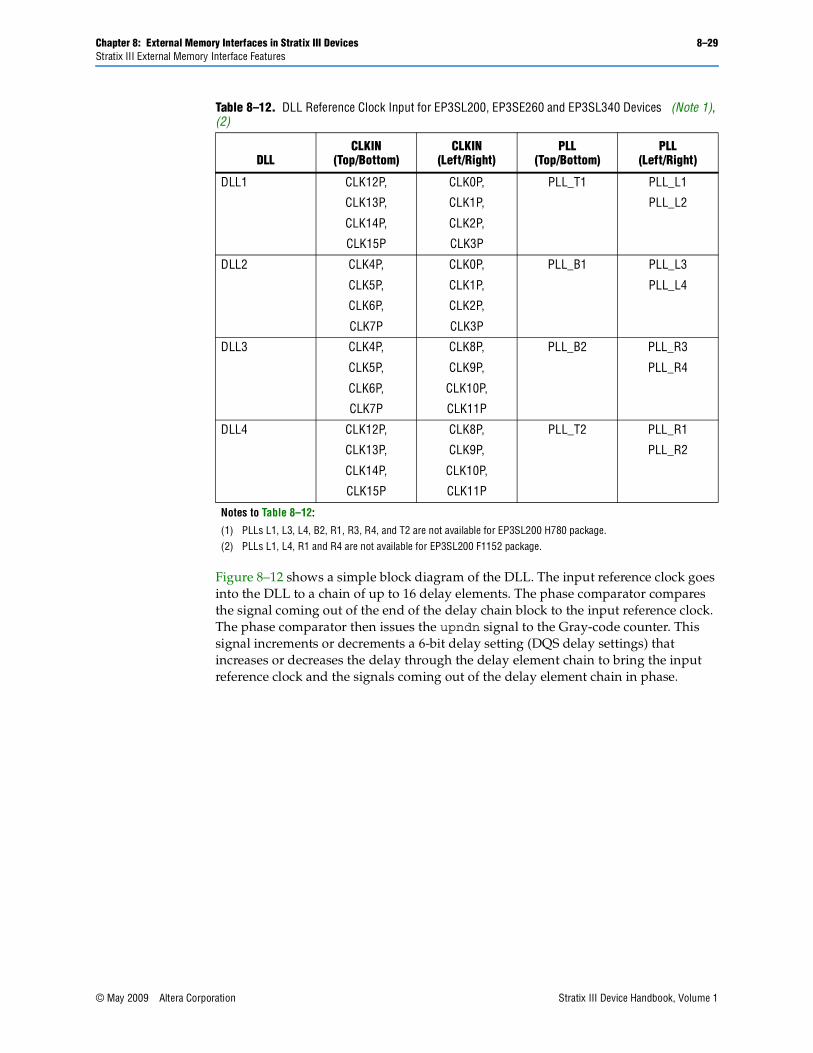
Table 8–12. DLL Reference Clock Input for EP3SL200, EP3SE260 and EP3SL340 Devices (Note 1), (2)
DLL CLKIN
(Top/Bottom)CLKIN
(Left/Right)PLL
(Top/Bottom)PLL
(Left/Right)
DLL1 CLK12P,
CLK13P,
CLK14P,
CLK15P
CLK0P,
CLK1P,
CLK2P,
CLK3P
PLL_T1 PLL_L1
PLL_L2
DLL2 CLK4P,
CLK5P,
CLK6P,
CLK7P
CLK0P,
CLK1P,
CLK2P,
CLK3P
PLL_B1 PLL_L3
PLL_L4
DLL3 CLK4P,
CLK5P,
CLK6P,
CLK7P
CLK8P,
CLK9P,
CLK10P,
CLK11P
PLL_B2 PLL_R3
PLL_R4
DLL4 CLK12P,
CLK13P,
CLK14P,
CLK15P
CLK8P,
CLK9P,
CLK10P,
CLK11P
PLL_T2 PLL_R1
PLL_R2
Notes to Table 8–12:
(1) PLLs L1, L3, L4, B2, R1, R3, R4, and T2 are not available for EP3SL200 H780 package.(2) PLLs L1, L4, R1 and R4 are not available for EP3SL200 F1152 package.
© May 2009 Altera Corporation Stratix III Device Handbook, Volume 1

8–30 Chapter 8: External Memory Interfaces in Stratix III DevicesStratix III External Memory Interface Features
The DLL can be reset from either the logic array or a user I/O pin. Each time the DLL is reset, you must wait for 1280 clock cycles before you can capture the data properly.
The DLL can shift the incoming DQS signals by 0°, 22.5°, 30°, 36°, 45°, 60°, 67.5°, 72°, 90°, 108°, 120°, 135°, 144°, or 180°, depending on the DLL frequency mode. The shifted DQS signal is then used as the clock for the DQ IOE input registers.
All DQS and CQn pins referenced to the same DLL can have their input signal phase shifted by a different degree amount but all must be referenced at one particular frequency. For example, you can have a 90° phase shift on DQS1T and a 60° phase shift on DQS2T referenced from a 200-MHz clock. Not all phase-shift combinations are supported, however. The phase shifts on the DQS pins referenced by the same DLL must all be a multiple of 22.5° (up to 90°), a multiple of 30° (up to 120°), a multiple of 36° (up to 144°), or a multiple of 45° (up to 180°).
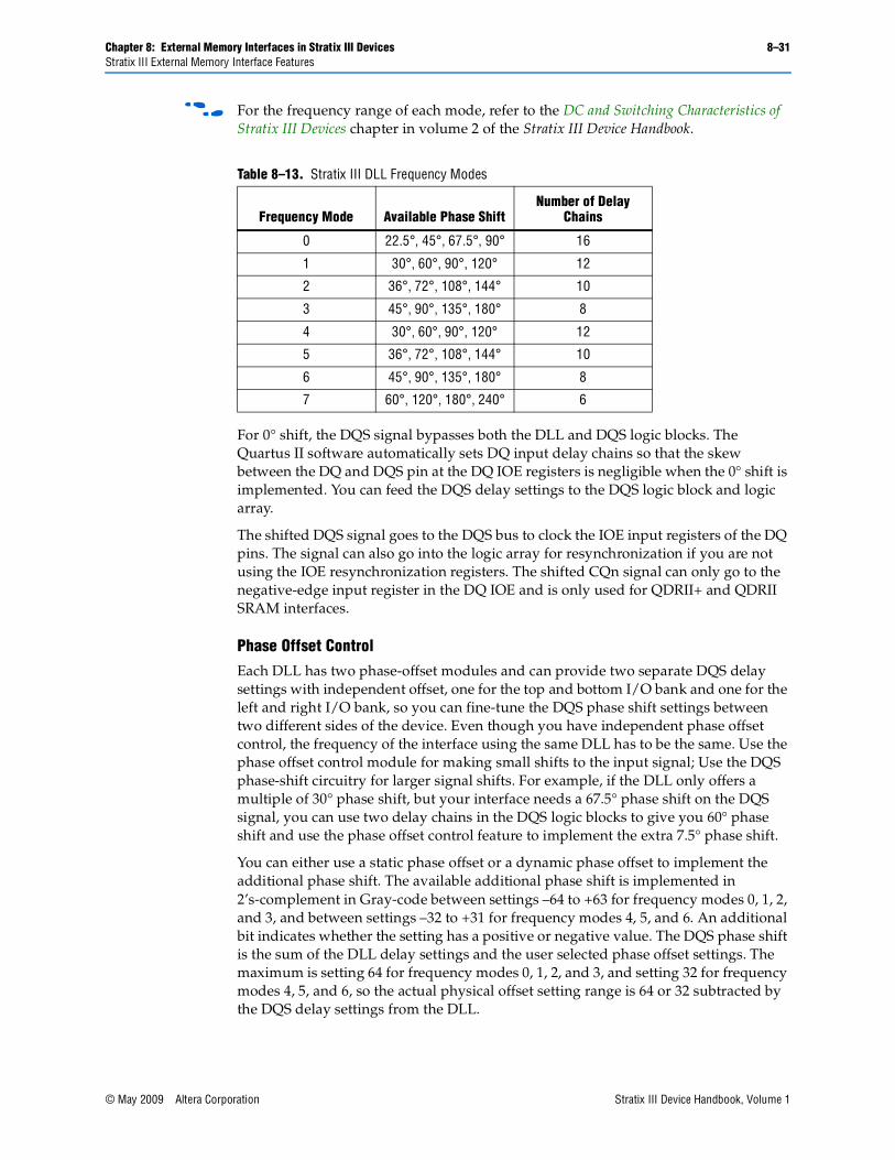
There are seven different frequency modes for the Stratix III DLL, as shown in Table 8–13. Each frequency mode provides different phase shift selections. In frequency modes 0, 1, 2, and 3, the 6-bit DQS delay settings vary with PVT to implement the phase-shift delay. In frequency modes 4, 5, and 6, only 5 bits of the DQS delay settings vary with PVT to implement phase-shift delay; the most significant bit of the DQS delay setting is set to 0.
Figure 8–12. Simplified Diagram of the DQS Phase Shift Circuitry (Note 1)
Notes to Figure 8–12:
(1) All features of the DQS phase-shift circuitry are accessible from the ALTMEMPHY megafunction in the Quartus II software. (2) The input reference clock for the DQS phase-shift circuitry can come from a PLL output clock or an input clock pin. Refer to Table 8–9 through
Table 8–12 for exact PLL and input clock pin location.(3) Phase offset settings can only go to the DQS logic blocks.(4) DQS delay settings can go to the logic array, the DQS logic block, and the leveling circuitry.
6
6
6
PhaseOffsetControl
6
Phase offset settingsfrom the logic array
Phase offsetsettings to DQS pinson top or bottom edge (3)
DQS DelaySettings (4)
Input ReferenceClock (2) upndn
clock enable
DLL
6
addnsub_a
PhaseComparator
Delay Chains
Up/DownCounter
6
PhaseOffsetControl
Phase offset settingsfrom the logic array
Phase offsetsettings to DQS pin on left or right edge (3)
6
addnsub_b
Stratix III Device Handbook, Volume 1 © May 2009 Altera Corporation
Chapter 8: External Memory Interfaces in Stratix III Devices 8–31Stratix III External Memory Interface Features
f For the frequency range of each mode, refer to the DC and Switching Characteristics of Stratix III Devices chapter in volume 2 of the Stratix III Device Handbook.
For 0° shift, the DQS signal bypasses both the DLL and DQS logic blocks. The Quartus II software automatically sets DQ input delay chains so that the skew between the DQ and DQS pin at the DQ IOE registers is negligible when the 0° shift is implemented. You can feed the DQS delay settings to the DQS logic block and logic array.
The shifted DQS signal goes to the DQS bus to clock the IOE input registers of the DQ pins. The signal can also go into the logic array for resynchronization if you are not using the IOE resynchronization registers. The shifted CQn signal can only go to the negative-edge input register in the DQ IOE and is only used for QDRII+ and QDRII SRAM interfaces.
Phase Offset ControlEach DLL has two phase-offset modules and can provide two separate DQS delay settings with independent offset, one for the top and bottom I/O bank and one for the left and right I/O bank, so you can fine-tune the DQS phase shift settings between two different sides of the device. Even though you have independent phase offset control, the frequency of the interface using the same DLL has to be the same. Use the phase offset control module for making small shifts to the input signal; Use the DQS phase-shift circuitry for larger signal shifts. For example, if the DLL only offers a multiple of 30° phase shift, but your interface needs a 67.5° phase shift on the DQS signal, you can use two delay chains in the DQS logic blocks to give you 60° phase shift and use the phase offset control feature to implement the extra 7.5° phase shift.
You can either use a static phase offset or a dynamic phase offset to implement the additional phase shift. The available additional phase shift is implemented in 2’s-complement in Gray-code between settings –64 to +63 for frequency modes 0, 1, 2, and 3, and between settings –32 to +31 for frequency modes 4, 5, and 6. An additional bit indicates whether the setting has a positive or negative value. The DQS phase shift is the sum of the DLL delay settings and the user selected phase offset settings. The maximum is setting 64 for frequency modes 0, 1, 2, and 3, and setting 32 for frequency modes 4, 5, and 6, so the actual physical offset setting range is 64 or 32 subtracted by the DQS delay settings from the DLL.
Table 8–13. Stratix III DLL Frequency Modes
Frequency Mode Available Phase ShiftNumber of Delay
Chains
0 22.5°, 45°, 67.5°, 90° 16
1 30°, 60°, 90°, 120° 12
2 36°, 72°, 108°, 144° 10
3 45°, 90°, 135°, 180° 8
4 30°, 60°, 90°, 120° 12
5 36°, 72°, 108°, 144° 10
6 45°, 90°, 135°, 180° 8
7 60°, 120°, 180°, 240° 6
© May 2009 Altera Corporation Stratix III Device Handbook, Volume 1

8–32 Chapter 8: External Memory Interfaces in Stratix III DevicesStratix III External Memory Interface Features
1 When using this feature, you need to monitor the DQS delay settings to know how many offsets you can add and subtract in the system. Note that the DQS delay settings output by the DLL are also Gray-coded.
For example, if the DLL determines that DQS delay settings of 28 is needed to achieve a 30° phase shift in DLL frequency mode 1, you can subtract up to 28 phase offset settings and you can add up to 35 phase offset settings to achieve the optimal delay that you need. However, if the same DQS delay settings of 28 is needed to achieve 30° phase shift in DLL frequency mode 4, you can still subtract up to 28 phase offset settings, but you can only add up to 3 phase offset settings before the DQS delay settings reach their maximum settings because DLL frequency mode 4 only uses 5-bit DLL delay settings.
f For more information about the value for each step, refer to the DC and Switching Characteristics of Stratix III Devices chapter in volume 2 of the Stratix III Device Handbook.
When using static phase offset, you can specify the phase offset amount in the ALTMEMPHY megafunction as a positive number for addition or a negative number for subtraction. You can also have a dynamic phase offset that is always added to, subtracted from, or both added to and subtracted from the DLL phase shift. When you always add or subtract, you can dynamically input the phase offset amount into the dll_offset[5..0] port. When you want to both add and subtract dynamically, you control the addnsub signal in addition to the dll_offset[5..0] signals.
Stratix III Device Handbook, Volume 1 © May 2009 Altera Corporation

Chapter 8: External Memory Interfaces in Stratix III Devices 8–33Stratix III External Memory Interface Features
DQS Logic BlockEach DQS and CQn pin is connected to a separate DQS logic block, which consists of the DQS delay chains, update enable circuitry, and DQS postamble circuitry, as shown in Figure 8–13.
DQS Delay ChainThe DQS delay chains consist of a set of variable delay elements to allow the input DQS/CQ and CQn signals to be shifted by the amount specified by the DQS phase-shift circuitry or the logic array. There are four delay elements in the DQS delay chain; the first delay chain closest to the DQS/CQ pin can either be shifted by the DQS delay settings or by the sum of the DQS delay setting and the phase-offset setting. The number of delay chains required is transparent because the ALTMEMPHY megafunction automatically sets it when you choose the operating frequency. The DQS delay settings can come from the DQS phase-shift circuitry on either end of the I/O banks or from the logic array.
Figure 8–13. Stratix III DQS Logic Block
Notes to Figure 8–13:
(1) The input reference clock for the DQS phase-shift circuitry can come from a PLL output clock or an input clock pin. Refer to Table 8–9 through Table 8–12 for the exact PLL and input clock pin location.
(2) The dqsenable signal can also come from the Stratix III FPGA fabric.
D QD QUpdate Enable Circuitry
66
66
6 6
DQS delaysettings from the
DQS phase-shift circuitry
DQS orCQn Pin
Input ReferenceClock (1)
DQS Delay Chain
Bypass
Phase offsetsettings from
DQS phase shift circuitry
6
6
DQS Enable
gated_dqs control
DQS bus
PRN
CLR
Q
DFF
reset
AB VCC
DQS'
D
PostambleEnable
ResynchronizationClock
PostambleClock
dqsenable (2)
D
D D
Q
Q Q
© May 2009 Altera Corporation Stratix III Device Handbook, Volume 1

8–34 Chapter 8: External Memory Interfaces in Stratix III DevicesStratix III External Memory Interface Features
Delay elements in the DQS logic block have the same characteristics as the delay elements in the DLL. When the DLL is not used to control the DQS delay chains, you can input your own Gray-coded 6-bit or 5-bit settings using the dqs_delayctrlin[5..0]signals available in the ALTMEMPHY megafunction. These settings control 1, 2, 3, or all 4 delay elements in the DQS delay chains. The ALTMEMPHY megafunction can also dynamically choose the number of DQS delay chains needed for the system. The amount of delay is equal to the sum of the delay element’s intrinsic delay and the product of the number of delay steps and the value of the delay steps.
You can also bypass the DQS delay chain to achieve 0° phase shift.
Update Enable CircuitryBoth the DQS delay settings and phase-offset settings pass through a register before going into the DQS delay chains. The registers are controlled by the update enable circuitry to allow enough time for any changes in the DQS delay setting bits to arrive at all the delay elements. This allows them to be adjusted at the same time. The update enable circuitry enables the registers to allow enough time for the DQS delay settings to travel from the DQS phase-shift circuitry or core logic to all the DQS logic blocks before the next change. It uses the input reference clock or a user clock from the core to generate the update enable output. The ALTMEMPHY megafunction uses this circuit by default. See Figure 8–14 for an example waveform of the update enable circuitry output.
DQS Postamble CircuitryFor external memory interfaces that use a bi-directional read strobe like DDR3, DDR2, and DDR SDRAM, the DQS signal is low before going to or coming from a high-impedance state. The state where DQS is low, just after a high-impedance state, is called the preamble; The state where DQS is low, just before it returns to a high-impedance state, is called the postamble. There are preamble and postamble specifications for both read and write operations in DDR3, DDR2, and DDR SDRAM.
The DQS postamble circuitry, shown in Figure 8–15, ensures that data is not lost when there is noise on the DQS line at the end of a read postamble time. Stratix III devices have a dedicated postamble register that can be controlled to ground the shifted DQS signal used to clock the DQ input registers at the end of a read operation. This ensures that any glitches on the DQS input signals at the end of the read postamble time do not affect the DQ IOE registers.
Figure 8–14. Example of a DQS Update Enable Waveform
Update Enable Circuitry Output
System Clock
DQS Delay Settings(Updated every 8 cycles)
DLL Counter Update(Every 8 cycles)
6 bit
DLL Counter Update(Every 8 cycles)
Stratix III Device Handbook, Volume 1 © May 2009 Altera Corporation

Chapter 8: External Memory Interfaces in Stratix III Devices 8–35Stratix III External Memory Interface Features
In addition to the dedicated postamble register, Stratix III devices also have an HDR block inside the postamble enable circuitry. These registers are used if the controller is running at half the frequency of the I/Os.
Using the HDR block as the first stage capture register in the postamble enable circuitry block in Figure 8–15 is optional. The HDR block is clocked by the half-rate resynchronization clock, which is the output of the I/O clock divider circuit (shown in Figure 8–21 on page 8–39). There is an AND gate after the postamble register outputs that is used to avoid postamble glitches from a previous read burst on a non-consecutive read burst. This scheme allows a half-a-clock cycle latency for dqsenable assertion and zero latency for dqsenable deassertion, as shown in Figure 8–16.
Figure 8–15. Stratix III DQS Postamble Circuitry (Note 1)
Notes to Figure 8–15:
(1) The postamble clock can come from any of the delayed resynchronization clock taps although it is not necessarily of the same phase as the resynchronization clock.
(2) The dqsenable signal can also come from the Stratix III FPGA fabric.
DQS Enable
gated_dqs control
DQS Bus
PRN
CLR
Q
DFF
reset
AB VCC
DQS'
D
PostambleEnable
ResynchronizationClock
PostambleClock
D
D D
Q
Q Qdqsenable (2)
© May 2009 Altera Corporation Stratix III Device Handbook, Volume 1
8–36 Chapter 8: External Memory Interfaces in Stratix III DevicesStratix III External Memory Interface Features
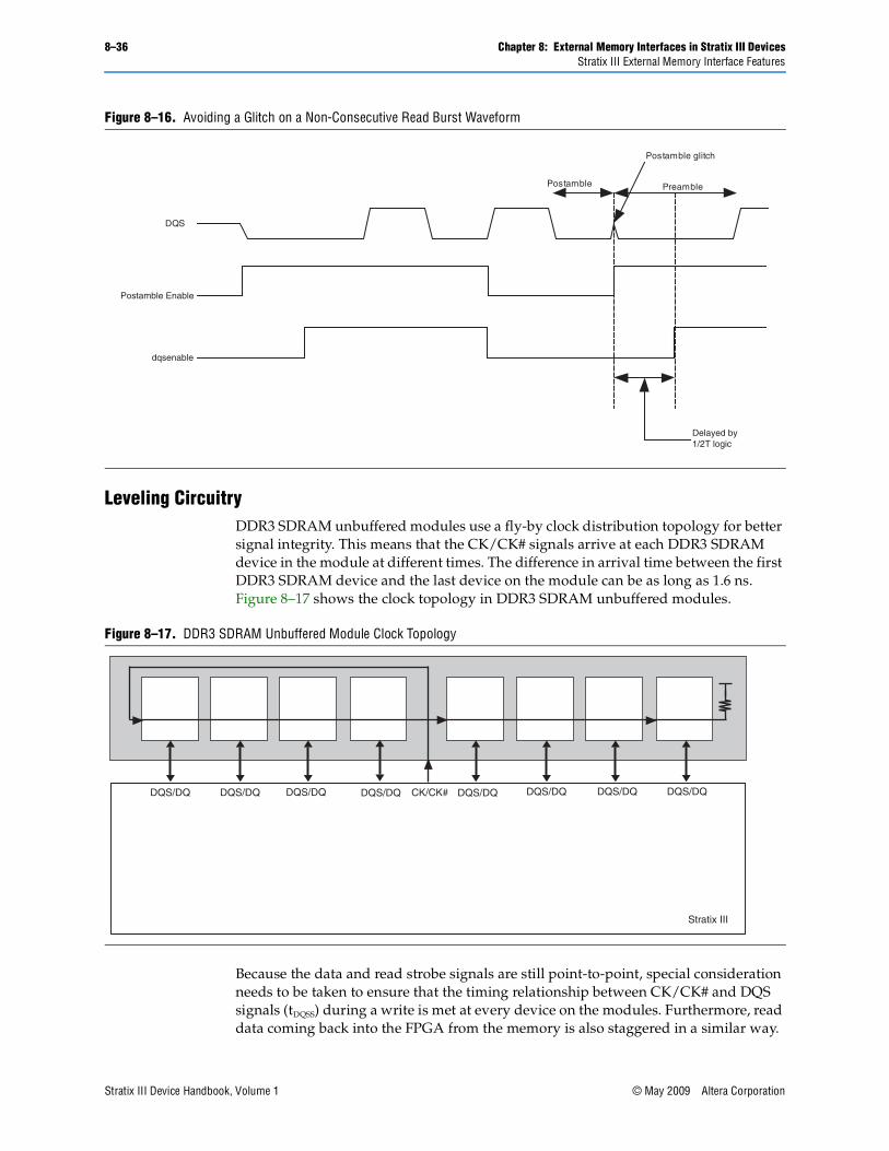
Leveling CircuitryDDR3 SDRAM unbuffered modules use a fly-by clock distribution topology for better signal integrity. This means that the CK/CK# signals arrive at each DDR3 SDRAM device in the module at different times. The difference in arrival time between the first DDR3 SDRAM device and the last device on the module can be as long as 1.6 ns. Figure 8–17 shows the clock topology in DDR3 SDRAM unbuffered modules.
Because the data and read strobe signals are still point-to-point, special consideration needs to be taken to ensure that the timing relationship between CK/CK# and DQS signals (tDQSS) during a write is met at every device on the modules. Furthermore, read data coming back into the FPGA from the memory is also staggered in a similar way.
Figure 8–16. Avoiding a Glitch on a Non-Consecutive Read Burst Waveform
Delayed by 1/2T logic
PreamblePostamble
Postamble glitch
DQS
Postamble Enable
dqsenable
Figure 8–17. DDR3 SDRAM Unbuffered Module Clock Topology
DQS/DQ DQS/DQDQS/DQDQS/DQDQS/DQ DQS/DQ CK/CK#
Stratix III
DQS/DQ DQS/DQ
Stratix III Device Handbook, Volume 1 © May 2009 Altera Corporation

Chapter 8: External Memory Interfaces in Stratix III Devices 8–37Stratix III External Memory Interface Features
Stratix III FPGAs have leveling circuitry to take care of these two needs. There is one group of leveling circuitry per I/O bank, with the same I/O number (for example, there is one leveling circuitry shared between I/O bank 1A, 1B, and 1C) located in the middle of the I/O bank. These delay chains are PVT-compensated by the same DQS delay settings as the DLL and DQS delay chains. For frequencies equal to and above 400 MHz, the DLL uses eight delay chains such that each delay chain generates a 45° delay.
The generated clock phases are distributed to every DQS logic block that is available in the I/O bank. The delay chain taps, then feeds a multiplexer controlled by the ALTMEMPHY megafunction to select which clock phases are to be used for that ×4 or ×8 DQS group. Each group can use a different tap output from the read-leveling and write-leveling delay chains to compensate for the different CK/CK# delay going into each device on the module.
Figure 8–18 illustrates the Stratix III write leveling circuitry.
Figure 8–19 illustrates the Stratix III read leveling circuitry.
The –90° write clock of the ALTMEMPHY megafunction feeds the write-leveling circuitry to produce the clock that generates the DQS and DQ signals. During initialization, the ALTMEMPHY megafunction picks the correct write-leveled clock for the DQS and DQ clocks for each DQS/DQ group after sweeping all the available clocks in the write calibration process. The DQ clock output is –90° phase-shifted compared to the DQS clock output.
Figure 8–18. Stratix III Write Leveling Delay Chains and Multiplexers (Note 1)
Note to Figure 8–18:
(1) There is only one leveling delay chain per I/O bank with the same I/O number (for example, I/O banks 1A, 1B, and 1C). You can only have one memory controller in these I/O banks when you use leveling delay chains.
Write clk(-900) Write-Leveled DQS Clock
Write-Leveled DQ Clock
Figure 8–19. Stratix III Read Leveling Delay Chains and Multiplexers (Note 1)
Note to Figure 8–19:
(1) There is only one leveling delay chain per I/O bank with the same I/O number (for example, I/O banks 1A, 1B, and 1C). You can only have one memory controller in these I/O banks when you use leveling delay chains.
DQS
Resynchronization clock
Half-Rate Resynchronization Clock
Read-Leveled Resynchronization Clock
I/O Clock Divider
Half-Rate Source Synchronous Clock
© May 2009 Altera Corporation Stratix III Device Handbook, Volume 1

8–38 Chapter 8: External Memory Interfaces in Stratix III DevicesStratix III External Memory Interface Features
Similarly, the resynchronization clock feeds the read-leveling circuitry to produce the optimal resynchronization and postamble clock for each DQS/DQ group in the calibration process. Resynchronization and the postamble clocks can use different clock outputs from the leveling circuitry. Output from the read-leveling circuitry can also generate the half-rate resynchronization clock that goes to the FPGA fabric.
1 The ALTMEMPHY megafunction calibrates the alignment for read and write leveling dynamically during the initialization process.
Dynamic On-Chip Termination ControlFigure 8–20 shows the dynamic OCT control block. The block includes all the registers needed to dynamically turn on OCT during a read and turn OCT off during a write.
f For more information, refer to “OCT” on page 8–42 or to the Stratix III Device I/O Features chapter in volume 1 of the Stratix III Device Handbook.
I/O Element (IOE) RegistersThe IOE registers have been expanded to allow source-synchronous systems to have faster register-to-register transfers and resynchronization. Both top/bottom and left/right IOEs have the same capability with left/right IOEs having extra features to support LVDS data transfer.
Figure 8–21 shows the registers available in the Stratix III input path. The input path consists of the DDR input registers, resynchronization registers, and HDR block. Each block of the input path can be bypassed.
Figure 8–20. Stratix III Dynamic OCT Control Block
Note to Figure 8–20:
(1) The write clock comes from either the PLL or the write leveling delay chain.
OCT Control
WriteClock (1)
OCT Enable
Resynchronization Registers
OCT Half-Rate Clock
OCT Control Path
DFFDFF
2
HDRBlock
Stratix III Device Handbook, Volume 1 © May 2009 Altera Corporation

Chapter 8:External M
emory Interfaces in Stratix
III Devices8–39
StratixIII External M
emory Interface Features
© M
ay 2009Altera Corporation
Stratix III Device Handbook, Volum
e 1
fed by the DQS bus or CQn bus.
DFF
DFF
D Q
D Q
DFF
D Q
DFF
DFF
D Q
D Q
DFF
D Q
Rate Registers
To Core (rdata0) (7)
To Core (rdata1)
(7)
To Core (rdata2)(7)
To Core (rdata3)
(7)
to core (7)
chronization Clock (resync_clk_1x)
0
1
dataoutbypass(8)
0
1
Figure 8–21. Stratix III IOE Input Registers (Note 1)
Notes to Figure 8–21:
(1) You can bypass each register block in this path.(2) This is the 0-phase resynchronization clock (from the read-leveling delay chain).(3) The input clock can be from the DQS logic block (whether the postamble circuitry is bypassed or not) or from a global clock line.(4) This input clock comes from the CQn logic block.(5) This resynchronization clock can come either from the PLL or from the read-leveling delay chain.(6) The I/O clock divider resides adjacent to the DQS logic block. In addition to the PLL and read-leveled resync clock, the I/O clock divider can also be (7) The half-rate data and clock signals feed into a dual-port RAM in the FPGA core.(8) You can dynamically change the dataoutbypass signal after configuration.
DFF
I
DFF
Input Reg A
Input Reg B
neg_reg_out
I
D Q
D Q
0
1
DQS (3)
CQn (4)
DQ
Input Reg CI
DFF
D Q
ResynchronizationClock(resync_clk_2x)(5)
Alignment & Synchronization Registers
Double Data Rate Input Registers
Half Data
Half-Rate Resyn
I/O Clock Divider (6)
(2)
DFF
D Q
DFF
D Q
DFF
D Q
DFF
D Q
DFF
D Q
DFF
D Q
DFF
D Q
DFF
D Q
DQSn
DifferentialInputBuffer
0..7
8–40 Chapter 8: External Memory Interfaces in Stratix III DevicesStratix III External Memory Interface Features
There are three registers in the DDR input registers block. Two registers capture data on the positive and negative edges of the clock, while the third register aligns the captured data. You can choose to have the same clock for the positive edge and negative edge registers, or two different clocks (DQS for positive edge register, and CQn for negative edge register). The third register that aligns the captured data uses the same clock as the positive edge registers.
Resynchronization registers consist of up to three levels of registers to resynchronize the data to the system clock domain. These registers are clocked by the resynchronization clock that is either generated by the PLL or the read-leveling delay chain. The outputs of the resynchronization registers can go straight to the core or to the HDR blocks, which are clocked by the divided-down resynchronization clock.
For more information about the read-leveling delay chain, refer to “Leveling Circuitry” on page 8–36.
Figure 8–22 shows the registers available in the Stratix III output and output-enable paths. The path is divided into the HDR block, resynchronization registers, and output/output-enable registers. The device can bypass each block of the output and output-enable path.
Stratix III Device Handbook, Volume 1 © May 2009 Altera Corporation
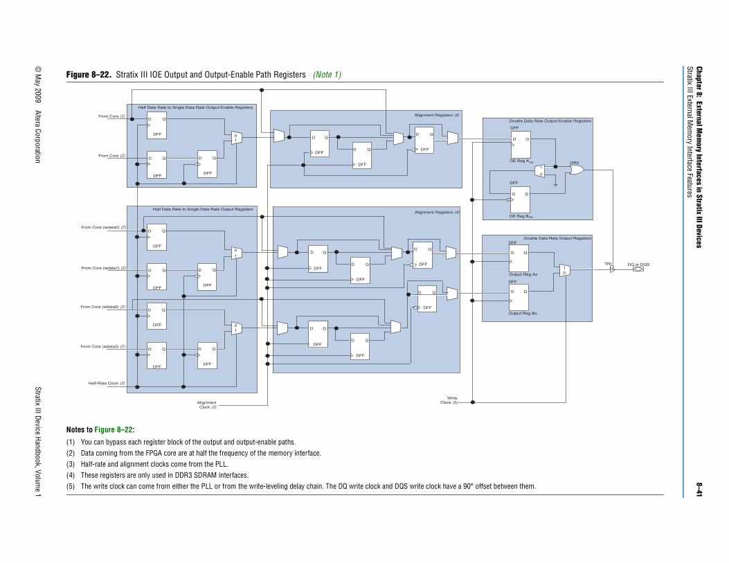
Chapter 8:External M
emory Interfaces in Stratix
III Devices8–41
StratixIII External M
emory Interface Features
© M
ay 2009Altera Corporation
Stratix III Device Handbook, Volum
e 1
een them.
D Q
DFF
D Q
DFF
01
Output Reg Ao
Output Reg Bo
D Q
DFF
D Q
DFF
OR2
TRI
OE Reg BOE
OE Reg AOE
0
1
Double Data Rate Output-Enable Registers
Double Data Rate Output Registers
DQ or DQS
Figure 8–22. Stratix III IOE Output and Output-Enable Path Registers (Note 1)
Notes to Figure 8–22:
(1) You can bypass each register block of the output and output-enable paths.(2) Data coming from the FPGA core are at half the frequency of the memory interface.(3) Half-rate and alignment clocks come from the PLL.(4) These registers are only used in DDR3 SDRAM interfaces.(5) The write clock can come from either the PLL or from the write-leveling delay chain. The DQ write clock and DQS write clock have a 90° offset betw
DFF
DFF
D Q
D Q
DFF
D Q
DFF
DFF
D Q
D Q
DFF
D Q
Half Data Rate to Single Data Rate Output Registers
DFF
DFF
D Q
D Q
DFF
D Q
Half Data Rate to Single Data Rate Output-Enable Registers
Alignment Registers (4)
AlignmentClock (3)
01
0
1
01
From Core (2)
From Core (2)
From Core (wdata0) (2)
From Core (wdata1) (2)
From Core (wdata2) (2)
From Core (wdata3) (2)
WriteClock (5)
Half-Rate Clock (3)
DFF
D Q
DFF
D Q DFF
D Q
Alignment Registers (4)
DFF
D Q
DFF
D Q DFF
D Q
DFF
D Q
DFF
D Q
DFF
D Q

8–42 Chapter 8: External Memory Interfaces in Stratix III DevicesStratix III External Memory Interface Features
The output path is designed to route combinatorial or registered SDR outputs and full-rate or half-rate DDR outputs from the FPGA core. Half-rate data is converted to full-rate using the HDR block and is clocked by the half-rate clock from the PLL. Resynchronization registers are also clocked by the same 0° system clock, except in the DDR3 SDRAM interface where the leveling registers are clocked by the write-leveling clock.
For more information about the write leveling delay chain, refer to “Leveling Circuitry” on page 8–36.
The output-enable path has structure similar to the output path. You can have a combinatorial or registered output in SDR applications and you can use half-rate or full-rate operation in DDR applications. You also have the resynchronization registers similar to the output path registers structure, ensuring that the output-enable path goes through the same delay and latency as the output path.
IOE FeaturesThis section briefly describes how OCT, programmable delay chains, programmable output delay, slew rate adjustment, and programmable drive strength are useful in memory interfaces.
f For more information about the features listed below, refer to the Stratix III Device I/O Features chapter in volume 1 of the Stratix III Device Handbook.
OCTStratix III devices feature dynamic calibrated OCT, in which series termination (OCT RS) is turned on when driving signals and turned off when receiving signals, while the parallel termination (OCT RT) is turned off when driving signals and turned on when receiving signals. This feature complements the DDR3/DDR2 SDRAM on-die termination (ODT), whereby memory termination is turned off when the memory is sending data and turned on when receiving data. You can also use OCT for other memory interfaces to improve signal integrity.
1 You cannot use the programmable drive strength and programmable slew rate features when using OCT RS.
To use dynamic calibrated OCT, you must use the RUP and RDN pins to calibrate the OCT calibration block. You can use one OCT calibration block to calibrate one type of termination with the same VCCIO on the entire device. There are up to ten OCT calibration blocks to allow for different types of terminations throughout the device. For more information, refer to “Dynamic On-Chip Termination Control” on page 8–38.
1 You have the option to use the OCT RS feature with or without calibration. However, the OCT RT feature is only available with calibration.
You can also use the RUP and RDN pins as DQ pins. However, you cannot use the ×4 DQS/DQ groups where the RUP and RDN pins are located if you are planning to use dynamic calibrated OCT. The RUP and RDN pins are located in the first and last ×4 DQS/DQ group on each side of the device.
Stratix III Device Handbook, Volume 1 © May 2009 Altera Corporation

Chapter 8: External Memory Interfaces in Stratix III Devices 8–43Stratix III External Memory Interface Features
Use the OCT RT/RS setting for uni-directional read and write data; use a dynamic OCT setting for bi-directional data signals.
Programmable IOE Delay ChainsYou can use programmable delay chains in the Stratix III I/O registers as deskewing circuitry. Each pin can have a different input delay from the pin to input register or a delay from the output register to the output pin to ensure that the bus has the same delay going into or out of the FPGA. This feature helps read and write time margins as it minimizes the uncertainties between signals in the bus.
1 Deskewing circuitry and programmable IOE delay chains are the same circuit.
Programmable Output Buffer DelayIn addition to allowing output buffer duty cycle adjustment, the programmable output buffer delay chain allows you to adjust the delays between data bits in your output bus to introduce or compensate channel-to-channel skew. Incorporating skew to the output bus helps to minimize simultaneous switching events by enabling smaller parts of the bus to switch simultaneously, instead of the whole bus. This feature is particularly useful in DDR3 SDRAM interfaces where the memory system clock delay can be much larger than the data and data clock/strobe delay. Use this delay chain to add delay to the data and data clock/strobe to better match the memory system clock delay.
Programmable Slew Rate ControlStratix III devices provide four levels of static output slew rate control: 0, 1, 2, and 3, where 0 is the slowest slew rate setting and 3 is the fastest slew rate setting. The default setting for the HSTL and SSTL I/O standards is 3. A fast slew rate setting allows you to achieve higher I/O performance; a slow slew-rate setting reduces system noise and signal overshoot. This feature is disabled if you are using the OCT RS features.
Programmable Drive StrengthYou can choose the optimal drive strength needed for your interface after performing a board simulation. Higher drive strength helps provide a larger voltage swing, which in turn provides bigger eye diagrams with greater timing margin. However, higher drive strengths typically require more power, faster slew rates, and add to simultaneous switching noise. You can use programmable slew rate control along with this feature to minimize simultaneous switching noise with higher drive strengths.
This feature is disabled if you are using the OCT RS feature, which is the default drive strength in Stratix III devices. Use the OCT RT/RS setting for uni-directional read/write data; use the dynamic OCT setting for bi-directional data signals. You need to simulate the system to determine the drive strength needed for command, address, and clock signals.
© May 2009 Altera Corporation Stratix III Device Handbook, Volume 1

8–44 Chapter 8: External Memory Interfaces in Stratix III DevicesConclusion
PLLPLLs are used to generate the memory interface controller clocks, similar to the 0° system clock, the –90° or 270° phase-shifted write clock, the half-rate PHY clock, and the resynchronization clock. You can use the PLL reconfiguration feature to calibrate resynchronization phase shift to balance the setup and hold margin.
The VCO and counter setting combinations may be limited for high-performance memory interfaces.
f For more information about the Stratix III PLL, refer to the Clock Networks and PLLs in Stratix III Devices chapter in volume 1 of the Stratix III Device Handbook.
ConclusionStratix III devices have many features available to support existing and emerging external memory interfaces. The ALTMEMPHY megafunction, built to support the Stratix III memory interface features, allows you to easily implement your data path for use with either your own controller or Altera’s IP controller.
In Stratix III devices, most of the critical data transfers are taken care of for you in the IOE, alleviating the burden of having to close timing in the FPGA fabric. Furthermore, because most of the registers are in the IOE, data delays between registers are short, allowing the circuitry to work at a higher frequency. Dynamically calibrated OCT, slew rate adjustment, and programmable drive strength improve signal integrity, especially at higher frequencies of operation.
In addition, programmable delay chain and de-skew circuits allow Stratix III devices to achieve a better margin for high-performance memory interfaces. Dynamic calibration of resynchronization and postamble clocks guarantee high performance over PVT variations. Leveling circuitry enables Stratix III devices to support DDR3 modules, offering you the choice of highest-performance memory technologies. Stratix III devices also offer memory interface support in any of 24 modular I/O banks with up to four different frequencies of operations.
Stratix III Device Handbook, Volume 1 © May 2009 Altera Corporation

Chapter 8: External Memory Interfaces in Stratix III Devices 8–45Chapter Revision History
Chapter Revision HistoryTable 8–14 shows the revision history for this document.
Table 8–14. Chapter Revision History
Date and Revision Changes Made Summary of Changes
May 2009, version 1.8
■ Updated Table 8–1, Table 8–2, Table 8–3, Table 8–5, Table 8–7, and Table 8–13.
■ Updated Figure 8–3, Figure 8–4, Figure 8–5, Figure 8–6, and Figure 8–7.
■ Updated “DLL”, “Memory Interfaces Pin Support”, and “Rules to Combine Groups”sections.
—
February 2009,version 1.7
■ Updated Table 8–1,Table 8–2, and Table 8–6.
■ Updated “Data and Data-Strobe/Clock Pins” section.
■ Removed “Referenced Document” section.
—
October 2008, version 1.6
■ Updated Table 8–1, Table 8–2, Table 8–3, Table 8–4, Table 8–5, Table 8–7, and Table 8–8.
■ Updated the “Rules to Combine Groups”, “Phase Offset Control”, “OCT”, “Introduction”, “Memory Interfaces Pin Support”, “Combining ×16/×18 DQS/DQ groups for ×36 QDRII+/QDRII SRAM Interface”, “Rules to Combine Groups”, “DQS Phase-Shift Circuitry”, “DLL”, and “DQS Delay Chain” sections.
■ Updated Figure 8–2, Figure 8–4, Figure 8–10, Figure 8–21, and Figure 8–22.
■ Updated New Document Format.
■ Added (Note 3) to Table 8–5.
—
July 2008, version 1.5 Updated Table 8–1 and Table 8–2. —
May 2008, version 1.4
■ Updated Figure 8–2, Figure 8–9, Figure 8–18, Figure 8–21, and Figure 8–22.
■ Updated Table 8–1, Table 8–2, Table 8–3, Table 8–4, Table 8–7, and Table 8–10.
■ Added Table 8–7 and Table 8–8.
■ Added Figure 8–19.
■ Added new “Supporting ×36 QDRII+/QDRII SRAM Interfaces in the F780 and F1152-Pin Packages” section.
■ Updated “Data and Data Clock/Strobe Pins”.
■ Updated “Referenced Documents”.
Text, Table, and Figure updates.
November 2007, version 1.3
■ Updated Table 8–5.
■ Updated Figure 8–6.Minor updates to content.
© May 2009 Altera Corporation Stratix III Device Handbook, Volume 1
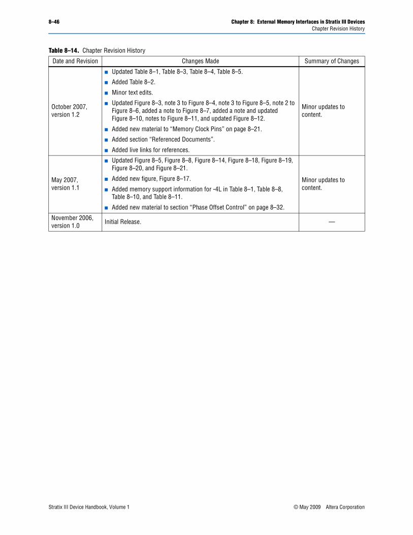
8–46 Chapter 8: External Memory Interfaces in Stratix III DevicesChapter Revision History
October 2007, version 1.2
■ Updated Table 8–1, Table 8–3, Table 8–4, Table 8–5.
■ Added Table 8–2.
■ Minor text edits.
■ Updated Figure 8–3, note 3 to Figure 8–4, note 3 to Figure 8–5, note 2 to Figure 8–6, added a note to Figure 8–7, added a note and updated Figure 8–10, notes to Figure 8–11, and updated Figure 8–12.
■ Added new material to “Memory Clock Pins” on page 8–21.
■ Added section “Referenced Documents”.
■ Added live links for references.
Minor updates to content.
May 2007,version 1.1
■ Updated Figure 8–5, Figure 8–8, Figure 8–14, Figure 8–18, Figure 8–19, Figure 8–20, and Figure 8–21.
■ Added new figure, Figure 8–17.
■ Added memory support information for -4L in Table 8–1, Table 8–8, Table 8–10, and Table 8–11.
■ Added new material to section “Phase Offset Control” on page 8–32.
Minor updates to content.
November 2006, version 1.0 Initial Release. —
Table 8–14. Chapter Revision History
Date and Revision Changes Made Summary of Changes
Stratix III Device Handbook, Volume 1 © May 2009 Altera Corporation