straw3 internal design reviewidlab/project_files/salt/... · 2003-09-13 · gary s. varner, straw3...
TRANSCRIPT

STRAW3Internal Design Review
Gary S. VarnerOn the whipping post
ID Lab12 SEP 2003

1Gary S. Varner, STRAW3 Internal Design Review, September 2003
Topics (1 hour + 1 hour)
• Review briefly where we are– Design parameters (da Specs)– What in STRAW2 & how well it works
• STRAW3– STRAW2 Problem Resolution– Design philosophy– R&D Plans
• Review Items (critical)– Triggering
• Threshold setting (DACs)• Performance expectations
– Trigger monitoring– On-chip ADC

2Gary S. Varner, STRAW3 Internal Design Review, September 2003
Original Proposed Signal Flow
LNA Gain
Digitize
Trigger
[GHz]1.2.3
[GHz].3 1.2

3Gary S. Varner, STRAW3 Internal Design Review, September 2003
RF Transient Recorder Specs
• >= 1GHz analog input bandwidth (200-1200MHz)
• multi-GSa/s sampling rate (Nyquist limit min.)
• minimum phase distortion for clean polarization
• dynamic range (>= 10 bits)
• internal Analog to Digital Conversion (ADC)
• short record length (100-200ns if optimally matched)
• self-triggering with fine threshold adjustment
• bi-polar triggering
• deadtimeless conclude multi-hit buffering needed
• LOW POWER!!

4Gary S. Varner, STRAW3 Internal Design Review, September 2003
STRAW2 Specifications
> 1GHz ind. Adj.256 ind. Adj.32 OR of 1616 multiplicity
1-2 GHz high+low12 32 bits/ch.
<=16 ms cascadeADC (SAR) bits
Digitize deadtime
High level thresholdLow level threshold
High level logicLow level logic
Comparator typeMonitor scalers
Trigger type
# SCA/channel# of channels# of RF inputsSampling rate
Analog Triggering
STRAW2 Design Parameters
Input bandwidth
• Unique in this design is the triggering requirements – High freq and bipolar
• Large latency strategy:– Multiple buffering

5Gary S. Varner, STRAW3 Internal Design Review, September 2003
Domino Ring Sampler (DRS)
input• If can keep the sampling jitter small enough (or can measure), no need for a TDC!
• Switched Capacitor Array (SCA)
• Free running domino wave, stopped with trigger
• Sampling speed 2 GHz (500ps/bin), trigger gate sampling gives 50ps timing resolution
• 1024 bins → 150ns waveform + 350ns delay
• Free running domino wave, stopped with trigger
• Sampling speed 2 GHz (500ps/bin), trigger gate sampling gives 50ps timing resolution
• 1024 bins → 150ns waveform + 350ns delay
Information courtesy of Stefan Ritt (PSI):For further info.: http://meg.web.psi.ch/doc/talks/s_ritt/may02_triumf/meg.ppt
6Gary S. Varner, STRAW3 Internal Design Review, September 2003
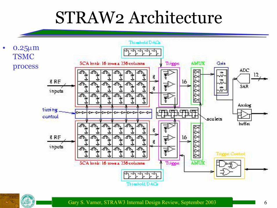
STRAW2 Architecture
• 0.25µm TSMC process

7Gary S. Varner, STRAW3 Internal Design Review, September 2003
STRAW2 Chip Self-Triggered Recorder Analog Waveform (STRAW)
32x256 SCA bank
DACs ADC
Trigger
scalers
16 Channels of256 deep SCA buckets
Optimized for RF inputMicrostrip 50Ω
Record length:128-256ns
Target input Bandwidth:>700MHz
-LL and HL (adj.) for each channel
Sampling Rate:1-2GSa/s (adj.)
-Multiplicity triggerfor LL hits
On-chip ADC:12-bit, >2MSPS
External option:MUXed Analog out
Sampling Rates>~8GSa/s possiblew/ 0.25µm process
8192 analog storage cells
Die:~2.5mm2
Self-Triggering:
Submitted for Fab.: 4 Nov., 2002

8Gary S. Varner, STRAW3 Internal Design Review, September 2003
STRAW2 Evaluation
• RF signal input
• Adjustable: 0.6 –3.4 GSa/s
• 256 samples (70 –300ns)

9Gary S. Varner, STRAW3 Internal Design Review, September 2003
Better than expected
STRAW2 Sampling Freq.
0
0.5
1
1.5
2
2.5
3
3.5
1 1.5 2 2.5 3
Freq. Adj. Voltage (ROVDD) [V]
Sam
plin
g Fr
eq. [
GH
z]
Avg.-cycle+cycleSPICE

10Gary S. Varner, STRAW3 Internal Design Review, September 2003
RF Response (1)
• Sub-ns transient ping: <= 100ps leading edge
Scope ET sampling:100 Gsa/s equiv.

11Gary S. Varner, STRAW3 Internal Design Review, September 2003
RF Response (2)
• Very nice tool: FFT analysis of RF transient pulse
• Have ideas how to improve –roll-off matches SPICE simulations of storage cells
1/8 ampl

12Gary S. Varner, STRAW3 Internal Design Review, September 2003
Analog Input Bandwidth –EST.
• Many examples of high sampling rate, but:– PMT readout– Wireless (2.5GHz)
– Very narrow BW
– Naïve calculation • phase• inductance
– 3-D Simulation• PCB, Package, bond wires• BGA necessary?• What is fundamental limit
Component Length/area Unit Factor FunitTotal [fF]
Input traces 5 cm 0.2 pF/cm 1000 w.a.g.bonding wire 150 mil 0.3 pF/wire 300 w.a.g.
input pad 60 um^2 187 fF/pad 187 Tannerinput protection 594 λ 1.1 pF/ckt 1100 SPICE
stripline area 2500 um^2 43aF/um^
2 107.5 MOSISstripline fringe 5 mm 60 aF/um 300 MOSISSwitch Drains 256 switches 5.6 fF/drain 1433.6 SPICE
Open Switches 6 open 87 fF/gate 522 SPICETOTAL 4.9501 pF
.2.32
13 GHz
RCf dB ==
πBonding wire, series R limit
.59.12
13 GHz
ZCf dB ==
πLumped element

13Gary S. Varner, STRAW3 Internal Design Review, September 2003
Analog B W Obtained
Cstore only 78fF !!
However, Ron ~ 3.2kΩ (SPICE)
.6372
13 MHz
RCf dB ==
πmVCkTvstore
rms 23.0==
DC SPICE sim shows can make Rstatic ~ 920Ω, but there is a dynamic component which is difficult to simulate accurately, conservatively assign 1kΩ
Use Ron = 1.9kΩ, adjust Cstore to 56fF
.48.12
13 GHz
RCf dB ==
π

14Gary S. Varner, STRAW3 Internal Design Review, September 2003
Good News: DC Power
<20mW/channel
DAC dominated

15Gary S. Varner, STRAW3 Internal Design Review, September 2003
STRAW2 Issues
• Extremely subtle error in on-chip ADC– Exact design worked in 5 previous designs
– “fixed” a symbol problem elsewhere
• Triggering– Problem with DAC load
– Focus of today’s review
• Input impedance– Target 50Ω, 130Ω actual (used wrong extracted parameter),
but makes the routing awkward, AND very low impedance
– Classical engineering trade-off • won’t discuss here unless time at the end
• Current BW OK for triggering, only tweak

16Gary S. Varner, STRAW3 Internal Design Review, September 2003
STRAW3 Design Philosophy
• Very conservative changes– Modest change to SCA array
– Implement fixes, no major rebuilding
• Key issue to be addressed is Triggering:– DAC setting ability (12-bit + 8-bit fine adjust)
– Sensitivity (overdrive, pulse width)
– Stability (choice of discrim. Op mode)
– Rate monitoring (scalers)
– On-chip multiplicity logic
– NEW: direct 16 of bits out for forming complex external trigger in firmware

17Gary S. Varner, STRAW3 Internal Design Review, September 2003
On-Chip ADC
• 12-bit SAR (Successive Approximation)– >= 5MSa/s rate– Performance limited by:
• Quality of R/2R match (DAC linearity/continuity)• DAC settling speed• Settling time of comparator
• Reasoning– Used successfully on 5 previous chip designs– All issues known
• What went wrong?– Like a plane crash, never a single failure:
• Subtle error in redefinition of 2 input digital MUX• SPICE simulation of WRONG extraction file

18Gary S. Varner, STRAW3 Internal Design Review, September 2003
ADC

19Gary S. Varner, STRAW3 Internal Design Review, September 2003
ADC SIMS

20Gary S. Varner, STRAW3 Internal Design Review, September 2003
Self-Triggering

21Gary S. Varner, STRAW3 Internal Design Review, September 2003
Digital-to-Analog Convert
Main DAC
Fine-adjust DAC
DAC Code

22Gary S. Varner, STRAW3 Internal Design Review, September 2003
Fine Adjust
R
“2R”

23Gary S. Varner, STRAW3 Internal Design Review, September 2003
Triggering Detail

24Gary S. Varner, STRAW3 Internal Design Review, September 2003
Discriminator Layout
Fast Comparator Control Logic Capacitor

25Gary S. Varner, STRAW3 Internal Design Review, September 2003
Simulation Results
• Use simulated high freq. Response from beamtest data:– works

26Gary S. Varner, STRAW3 Internal Design Review, September 2003
Simulation
27Gary S. Varner, STRAW3 Internal Design Review, September 2003
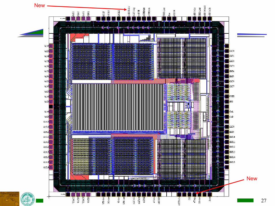
OverviewNew
New

28Gary S. Varner, STRAW3 Internal Design Review, September 2003
Summary
• If no show-stoppers– Submit STRAW3 before Monday– Full DRC done & preliminary MOSIS check– Only hang-up was M3 coverage (28.9% vs. 30% min.)
• Plans:– LABRADOR submission deferred (target 9/15-> 11/17)– Will continue to poke away at, probably ready for review
when I return from Japan– If this beneficial, do a similar
• Testing/firmware/software

29Gary S. Varner, STRAW3 Internal Design Review, September 2003
Back-up slides

30Gary S. Varner, STRAW3 Internal Design Review, September 2003
Askaryan Signature
0 2 4 6 8
Time (ns)
• Significant signal power at large frequencies
• Strong linear polarization (near 100%)

31Gary S. Varner, STRAW3 Internal Design Review, September 2003
RF Response

32Gary S. Varner, STRAW3 Internal Design Review, September 2003
High-speed Digitizers
• Kleinfelder speed but not high
analog BW
High Speed Digitizer Comparison
10
100
1000
10000
10 100 1000 10000
Analog Bandwidth [MHz]
Sam
plin
g R
ate
[MS
a/s]
ZEUS[12]RD2[13]Kleinfelder[14]Haller[15]ADeLine1[11]DSC/DRS[16]AD9410[17]CLC5957[18]TLV5580[19]ADS5102[20]MAX1449[21]
Desired Max.Operating Region
STRAW2• Analog BW tough
• Comm. ADC very high P

33Gary S. Varner, STRAW3 Internal Design Review, September 2003
Straw Man
Trigger/Digitizers

34Gary S. Varner, STRAW3 Internal Design Review, September 2003
Design Issues for Discussion
• RF amps/filter mounting– Directly onto back of antennas? (modular)
• Better performance, but power, cooling, cabling issues
– Miteq LNAs adequate?– Sufficient sensitivity (w/ power limit, multi-notch filters) ??
• Trigger architecture:– Global, local, cluster (half-array) ??– Logic on ARF boards ??– Multi-leveled ?? Multi-band ??– VETO ?? RCP & LCP generation ??
• Signal digitizing:– Random interleaving (longer record length) ??– Alternatives to current plan ??– Multi-buffering (ping-pong) depth ??

35Gary S. Varner, STRAW3 Internal Design Review, September 2003
RF Coupling Simulation
.4.62
13 GHz
RCf dB ==
π.4.6
21
3 GHzRC
f dB ==π
.4.62
13 GHz
RCf dB ==
π.4.6
21
3 GHzRC
f dB ==π
die
on-chip 50Ω stripline
Bonding wires
• Utilizes the LC program (FTDT algorithm)– Cray developed, available for free under Linux

36Gary S. Varner, STRAW3 Internal Design Review, September 2003
S-Parameters
STRAW2 Packaging S-Parameters
0
0.2
0.4
0.6
0.8
1
1.2
0 0.5 1 1.5 2 2.5 3
Frequency [GHz]
S11S21
VSWR:
1.8 [1GHz]
1.9 [2GHz]