structural and charge transport characteristics of graphene layers obtained from cvd thin film and...
TRANSCRIPT
C A R B O N 5 2 ( 2 0 1 3 ) 4 9 – 5 5
.sc ienced i rec t .com
Avai lab le a t wwwjournal homepage: www.elsevier .com/ locate /carbon
Structural and charge transport characteristics of graphenelayers obtained from CVD thin film and bulk graphitematerials
Anastasia V. Tyurnina a,*, Kazuhito Tsukagoshi b, Hidefumi Hiura b,c
Alexander N. Obraztsov a,d
a Department of Physics, M.V. Lomonosov Moscow State University, Moscow 119991, Russiab International Center for Materials Nanoarchitectonics, National Institute for Materials Science, Tsukuba 305-0044, Japanc Green Innovation Research Laboratories, NEC Corporation, Tsukuba 305-8501, Japand Department of Physics and Mathematics, University of Eastern Finland, Joensuu 80101, Finland
A R T I C L E I N F O
Article history:
Received 16 May 2012
Accepted 2 September 2012
Available online 8 September 2012
0008-6223/$ - see front matter � 2012 Elsevihttp://dx.doi.org/10.1016/j.carbon.2012.09.003
* Corresponding author: Fax: +33 438785117.E-mail address: [email protected]
A B S T R A C T
We report an experimental comparative study of graphene layers produced by microme-
chanical cleavage of bulk graphite materials of different origins and graphite films obtained
by plasma enhanced chemical vapor deposition (PECVD). Structural characteristics of these
materials were evaluated using Raman spectroscopy and electron microscopy. Field effect
transistors (FETs) based on the PECVD graphene were produced using electron beam lithog-
raphy. Conductivity, carrier mobility and other characteristics of the PECVD graphene
obtained from Raman and FET tests were similar to the properties of graphene flakes
obtained from bulk graphite materials. Taking into account the scalability of the CVD fab-
rication, these results confirm the possible industrial use of graphene films obtained by this
method.
� 2012 Elsevier Ltd. All rights reserved.
1. Introduction
Since the demonstration of the potential possibility to obtain
micrometer scale graphene [1], a lot of efforts have been de-
voted to develop fabrication of single (SLG) and few layer graph-
ene (FLG) films with scale and dimensions appropriate for
industrial application [2]. Because of high optical transparency
in a wide spectral range [3–5] and prominent electronic proper-
ties [6–10] graphene applications are expected in optical ele-
ments, optoelectronic and electronic devices with the typical
lateral dimensions up to dozens of centimeters (see, e.g.
[4,5,11]). However, the experimental investigations were per-
formed mainly for graphene samples produced by the tradi-
tional scotch tape method from highly oriented pyrolitic
graphite (HOPG), Kish graphite or natural graphite [1,6–10,
er Ltd. All rights reservedu (A.V. Tyurnina).
12–15]. The method of micromechanical cleavage requires a
high purity condition and allows obtaining only a limited size
flakes randomly located on the substrate. Thus, it is obvious,
that the scotch tape method is not suitable for industry produc-
tion due to its low reproducibility.
Various kinds of methods for graphene production were
proposed with use of silicon carbide surface graphitization
in an ultra-high vacuum [8,16], dissociation of gaseous hydro-
carbons on Ni(111) [17] or copper foils [11], etc. Among the
different approaches chemical vapor deposition (CVD) has
proven to be a promising technique due to its low cost and
ability to provide a high quality FLG films on the large area
substrates [2]. In our previous works a plasma enhanced
chemical vapor deposition (PECVD) has been developed as
the method for production of large area (up to few square
.

50 C A R B O N 5 2 ( 2 0 1 3 ) 4 9 – 5 5
centimeters with potentially large scalability) FLG, or graphite
of nanometer thickness [18]. Crystal ordering and specific
topology characteristics of the PECVD nanographite films
have been evaluated with use of Raman spectroscopy, scan-
ning (SEM), high resolution transmission electron microscopy
(HR TEM), and atomic force microscopy (AFM) [18,19]. In this
work, we study the structural properties of the PECVD graph-
ene in comparison with the SLG flakes produced from HOPG,
Kish graphite or natural graphite which are usually utilized in
the experimental investigations of graphene for field effect
transistor (FET), and we analyze electronic characteristics of
the FET produced using the PECVD graphene flakes.
Fig. 1 – Typical SEM image of the PECVD graphite film of few
nanometer thickness. The film consists of the atomically
flat domains separated from each other by the wrinkles
(bright lines).
2. Samples preparation and characterization
The samples of graphite films of nanometer thickness were
produced by the PECVD technique from a hydrogen and
methane gas mixture activated by a DC discharge. The de-
tailed description of this method is presented elsewhere
[18]. The graphite films were grown on square (10 · 10 mm)
substrates made of nickel sheets of about 0.5 mm thickness.
Those nickel sheets were produced by rolling of polycrystal-
line nickel. A gas mixture of hydrogen and methane (in pro-
portion of H2:CH4 = 100:5) was used in the PECVD procedure
with total pressure of about 10 Pa and with total gas flow of
about 500 sccm. To remove oxide layer and possible impuri-
ties from the nickel surface the substrates were exposed
initially in pure hydrogen plasma at the same pressure with
substrate temperature of about 900 �C during 15 min. After
that methane with proportion mentioned above was
introduced into the gas. The carbon deposition starts with
introduction of methane at the same substrate temperature
(of about 900 �C determined by an optical pyrometer) and con-
tinues for 5–10 min depending on desirable thickness of the
graphite film of nanometer thickness.
The micromechanical cleavage method similar to that de-
scribed in Ref. [1] was used to prepare graphene flakes from
different bulk graphite materials including HOPG (Furuuchi
Kagaku, Japan), Kish graphite (SPI West Chester, PA 19381,
USA), natural graphite (Madagascar graphite) and the PECVD
graphite films of nanometer thickness. The PECVD graphite
films were used as-grown without any special treatments
and without separation from the nickel substrate. The micro-
mechanically pilled out graphene flakes were transferred
onto the clean silicon substrate surface to perform a compar-
ative study of their structural and electrical properties. A low-
resistivity silicon wafer was used to prepare the substrates of
5 · 5 · 0.5 mm covered by 300 nm of silicon oxide layer. Usage
of this type of substrate allows determination the number of
graphene layer in transferred flakes through the analysis of
optical microscopy images [20,21].
Raman spectroscopy is a powerful tool to evaluate struc-
tural characteristics, defect presence and thickness of the
graphene samples. In order to compare the structural quality
of as-prepared graphene flakes, Raman investigation was per-
formed using T64000 Jobin Yvon instrument with the laser
excitation at wavelength of 514.5 nm. The optical microscopy
(OLYMPUS BX51) attached to the Raman spectrometer allows
the laser beam focusing to a spot size of 1–2 lm.
Electronic properties of the graphene layers prepared from
the PECVD graphene were evaluated by measuring the FET
characteristics. The FETs with the top and bottom gates elec-
trodes were produced using electron beam lithography (EBL)
facility ELIONIX ELS-7500RS similar to that described else-
where [22]. The samples were mounted on chip carriers and
sealed in a vacuum sample tube. During the measurements,
the sample tube was immersed in liquid nitrogen, and thus
the sample temperature was about 77 K.
The routine characterizations of as-grown PECVD graphite
film of nanometer thickness were performed using SEM (LEO
Supra 50 PV). The overall observation shows that the PECVD
film is more or less homogeneous on whole nickel substrate
surface with dimensions up to 20 · 20 mm. At micrometer
resolution (Fig. 1) the main topology features of the film are
the atomically flat domains with characteristic size of about
1 lm and the wrinkles between the domains. The typical
height of the wrinkles is about 30 nm. Previously we have
reported that the most probable reason for the origin of the
wrinkles is post-grown deformation of the PECVD films be-
cause of difference in the thermal expansion coefficients of
graphite and nickel [17,19]. At the same time in according to
Raman and AFM measurements the flat area domains have
atomically smooth surfaces approximately parallel to the
nickel substrate. These surfaces consist of highly ordered
FLG films with thickness varying between one to tens graph-
ene layers [17,19].
3. Results and discussion
Four graphene fragments for each type of graphite sources
were selected using an optical microscopy [20,21] to carry
out subsequent comparative study of their properties. The
typical optical images of the handpicked objects are shown
in Fig. 2. The microphotos were analyzed by the image pro-
cessing program ‘‘ImageJ 1.37v’’ to determine the number
and the size of graphene layers in these samples. We were
able to prepare uniform graphene monolayers peeled off from
the PECVD graphite film of nanometer thickness and from
Kish graphite (see examples in Fig. 2a and c, correspondingly).
The FLG fragments with different number of graphene mono-
layers of 1–5 were produced from HOPG and from natural

Fig. 2 – Typical optical micrograph images of graphene flakes obtained from PECVD and different graphite sources by the
micromechanical cleavage with the use of the scotch tape and transferred onto the oxidized silicon wafer: (a) PECVD graphite
film of nanometer thickness, (b) HOPG, (c) Kish graphite and (d) natural graphite.
C A R B O N 5 2 ( 2 0 1 3 ) 4 9 – 5 5 51
graphite (see examples in Fig. 2b and d, correspondingly). Pre-
sented in Fig. 2 FLG flakes contain the monolayer thickness
area with dimensions large enough to focus inside it the laser
beam during Raman spectroscopy measurements (i.e. more
than 2 lm).
Raman spectra of graphene samples produced from differ-
ent graphite materials are presented in Fig. 3. The spectra re-
corded in a range of 1000–3000 cm�1 are typical for a SLG with
the G peak position at around 1580 cm�1 and the 2D band of
second-order scattering located at around 2700 cm�1 [18,23].
1350 1425 1500 1575 2600 2650 2700 2750
43
21
Inte
nsity
, a. u
.
D G
2D
Raman Shift, cm-1
1 Kish - graphite2 PECVD3 HOPG4 Natural graphite
Fig. 3 – Raman spectra obtained for the graphene samples
produced from different graphite materials and deposited
into on Si:SiO2 (300 nm) substrates. The spectra were
normalized to the intensity of the G peak and shifted for
visibility along the Y axis (intensity).
There is no signal detected above the noise level at the Raman
shift frequency corresponding to, so called, ‘disordered graph-
ite line D’ at about 1350 cm�1. These peculiarities indicate
rather perfect graphene material crystallinity at least in the
area size comparable with the dimensions of excitation laser
beam spot (about 1–2 lm). All spectra presented in Fig. 3 were
normalized to the intensity of the G peak. For clear visibility
baselines of the Raman spectra 2, 3, and 4 are shifted (down)
along the Y axis (intensity). The profiles of the Raman bands
were fitted by the Lorentzian shapes and obtained fitting
parameters are shown in Table 1: position – m, full width at
half maximum (FWHM) – Dm and ratio of intensities for the
lines G and 2D – IG/I2D. The values of these fitting parameters
were determined with accuracy better than 0.1%. The shape
analysis of the 2D line confirms that all selected graphene
fragments (or investigated area of those) consist of a mono-
layer of graphene. Their crystallography perfection is con-
firmed additionally by the value of the 2D peaks intensity
which is much higher than that of the G-lines (see data of
IG/I2D in Table 1). Raman spectra analysis shows that the prop-
erties of the graphene samples produced from the PECVD
graphite films possesses crystallographic perfection compa-
rable with that of graphene flakes peeled off from graphite
materials of other types.
At the same time the presence of some minor difference in
Raman spectra should be noted. These differences are the
most evident in the form and position of the G line of Raman
spectrum for the graphene flake produced from natural
graphite (spectrum 4 in Fig. 3). FWHM value of the G line for
this type of graphene samples is about 6.2 cm�1 which is
much smaller than FWHM values of the G lines of Raman
spectra of other types of the graphene sample. In addition,
the G line for the natural graphite samples is shifted towards
higher frequencies and the intensity ratio IG/I2D is relatively
higher (see Table 1) in comparison with those of the other

Table 1 – Raman spectra parameters obtained from fitting of experimental data presented in Fig. 3 for SLG on Si:SiO2 (300 nm)substrates.
Source of graphene Raman spectrum parameters
mG, cm�1 DmG, cm�1 m2D, cm�1 Dm2D, cm�1 IG/I2D
Kish graphite 1579 14.8 2671 29.5 0.143PECVD 1581 9.9 2669 25.1 0.14HOPG 1581 10.0 2672 26.4 0.144Natural graphite 1588 6.2 2674 24.9 0.18
52 C A R B O N 5 2 ( 2 0 1 3 ) 4 9 – 5 5
samples. Taking into account that the Raman measurements
were carried out under the same conditions for all samples,
one can be sure that relative variations in the Raman peaks
positions of the samples of graphene produced from natural
graphite could not originate from their heating by the laser
radiation. Simultaneously detected frequency shift, decrease
of the line width and increase of the IG/I2D ratio may be ex-
plained as a result of the presence of impurities in the graph-
ene samples. Such impurities are well known to provide
changes of electrical conductivity via doping [24]. Also, such
kind of impurities in SLG or FLG might lead to the significant
reduction of charge carrier mobility [24]. We further empha-
size that all these relatively minor deviations in the Raman
spectrum were only detected for the graphene sample ob-
tained from natural graphite. All other investigated graph-
enes were produced from the artificially synthesized
graphite samples. The artificial production suggests forma-
tion of graphite under controlled (clean) conditions. Thus,
the observed differences in Raman spectrum of graphene
flakes peeled off from natural graphite can be assigned to
the impurities presented in the natural material formed
without any special control.
Another distinctive feature is observed for Raman spec-
trum of graphene prepared from Kish graphite (curve 1 in
Fig. 3). The G band has FWHM is about 15 cm�1, that is wider
in comparison with those of other types of the graphene sam-
ples, where this value did not exceed 10 cm�1 (see Table 1).
This Raman line width increase corresponds to relatively
Fig. 4 – (a) Optical micrograph images of (a) few PECVD graphene
wafer and (b) FET device prepared from the SLG flake. The locati
the flake shown in image (a) is marked with black dotted line. So
by thermal deposition of Ti/Au layers of 5 and 50 nm thickness, r
e-beam deposition of Al layer of 30 nm thickness; 5 nm Al2O3 top
Schematic view of the dual gate configuration of fabricated FET
and channel length of 9 lm. (For interpretation of the references
version of this article.)
poorer structural ordering that can also influence the carrier
mobility. Despite of the noted differences, obtained Raman
spectra indicate that all the samples have quite similar struc-
tural characteristics which are specific for rather high ordered
single graphene layer.
In order to examine the electronic properties of the PECVD
graphene layers, we manufactured and characterized SLG
based field effect transistor device. The parameters of the
fabricated FET device were compared with those reported in
previous publications for similar devices produced from other
types of graphite materials [25,26]. Fig. 4a shows the optical
image of initial PECVD SLG flake. SLG based FET devices were
fabricated with EBL technique and one of the optical micro-
photos is presented in Fig. 4b The double gate electrode con-
figuration, schematically shown in Fig. 4c, was used for the
FET fabrication similar to that described elsewhere [22]. The
electrode configuration of the FET, presented in Fig. 4b, was
realized using EBL. Four contacts (numbered 8, 19, 4 and 3
in Fig. 4b) made of titanium and gold layers of 5 and 50 nm
thicknesses correspondingly, were evaporated onto the sur-
face of the PECVD graphene fragment from Fig. 4a Four con-
tacts configuration of FET allows elimination of the contact
resistance influence on the charge transport characteristic
measurements. The top electrode and gate (numbered 2 in
Fig. 4b) were formed by exposing on air of 30 nm alumina
layer. The top gate Al layer produced by e-beam sputtering
is oxidized for several hours under air exposure to form a thin
(�5 nm) top gate dielectric layer of Al2O3 [22].
flakes on top of an oxidized (300 nm of SiO2) highly doped Si
on of area from (a) is denoted by dashed line; the contour of
urce and drain contacts, marked as 3, 4, 8 and 19 are formed
espectively. The top gate electrode, marked as 2, is formed by
gate dielectric was formed by exposing the sample to air. (c)
device. As-prepared FET device has channel width of 2 lm
to color in this figure legend, the reader is referred to the web
-0.5 0.0 0.5 1.0 1.5
0.2
0.4
0.6
I sd.µ
A
Vtg. V-0.5 0.0 0.5 1.0 1.5
1x10⁵
2x10⁵
3x10⁵
4x10⁵
5x10⁵
Vtg. V
R. Ohm(a) (b)
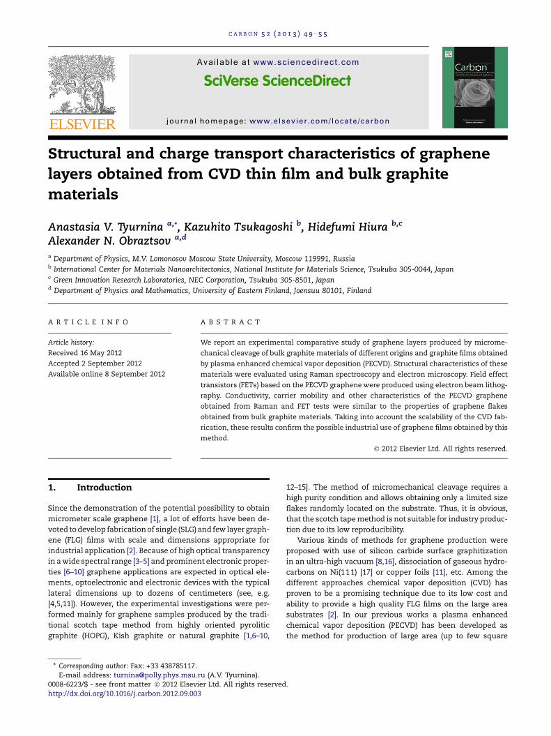
Fig. 5 – (a) Dual-gate transfer curve of the PECVD graphene FET formed on the Si substrate covered by 300 nm SiO2. The
current was measured for both positive and negative top-gate voltages. (b) Typical ambipolar dependence of SLG resistance R
on the top gate voltage Vtg. The measurements were performed at constant bottom gate voltage Vbg value of 30 V.
Table 2 – Charge carrier mobilities, obtained from charac-teristics of FET made of graphenes deposited onto Sisubstrates covered by 300 nm SiO2 (except the FET fabri-cated from suspended graphene).
References Characteristics of FET device
Size of FET devices,(channel width ·
channel length) lm2
Charge carriermobility,
cm2/V s; (on/offresistance ratio)
Current work 9 · 2 5 · 103; (�50)[12] (Suspendedgraphene)
N/A 106; (N/A)
[25] (APCVD) 1 · 3 3.8 · 103; (N/A)[29] (APCVD) 4 · 6 4 · 103; (�1,5)[11] (LPCVD) 3 · 2 7 · 103; (�14)[30] (LPCVD) 5 · 2 2.7 · 103; (�6)
C A R B O N 5 2 ( 2 0 1 3 ) 4 9 – 5 5 53
The charge carriers transport characteristics of as-pre-
pared FET fabricated using the PECVD graphene (Fig. 4) were
investigated using a 6-probe station under liquid nitrogen
temperature of 77 K. Fig.5 shows the resulting (a) dual-gate
transfer curve and (b) RV dependence. The current was mea-
sured for both positive and negative top-gate voltages. The
gate leak current was typically 10 nA which was much smaller
than the current between the source and drain (�1 lA). A
charge carrier inversion peak at the top gate voltage of about
0.5 V has been observed. This voltage value corresponds to
the Dirac point position which can be shifted from 0 V due
to several factors explained elsewhere [27]. In Fig. 5b, depen-
dence of the PECVD graphene resistance, R, on the voltage ap-
plied to the top gate, Vtg is represented. The characteristic of
PECVD graphene based FET is typical for a strong ambipolar
electric field effect, which is as well commonly observed for
the FET prepared using graphene flakes peeled off from HOPG
or natural graphite [1,28]. By analyzing presented transport
characteristics we can conclude that the electrical properties
of charge carriers in the PECVD graphene are similar to that
observed in graphene layers produced from other types of
graphite (HOPG, Kish graphite, natural graphite) [1,28,30].
Based on the data of the IV dependence, Fig. 5a, the electron
and hole carrier mobility estimations were performed using
the formula: (dIsd/dVgate)|Vsd = W * l * C0 * Vsd/L [31]. Here
(dIsd/dVgate) is taken from linear parts of IV curve, W and L
are width and length of the channel, l – mobility, C0 – capac-
itance. The mobility values in our experiments were 2700 and
5000 cm2/V s for electrons and holes, respectively. These val-
ues are lower than the record one shown for suspended
graphene flake exfoliated from natural graphite [12] (see
Table 2), yet still quite high in comparison to state of the art
Si based FETs. Thus, one can conclude that PECVD single-
and multi-graphene flakes are very attractive for practical
application in FET based circuits. Also it should be mentioned
that investigated FET device demonstrated on/off resistance
ratio around �50, which is typical for recent graphene based
FET devices (Table 2). It is well known that the poor on/off ra-
tio of graphene resulting from its zero band gap and the per-
spective to improve that value is another challenge topic,
described in [32,33].
Similar results for on/off ratio and mobility values have
been demonstrated recently for FET devices manufactured
using graphene synthesized by low pressure thermal CVD
(LPCVD) and atmospheric pressure thermal CVD (APCVD) on
copper foils (Table 2). These types of CVD techniques are con-
sidered nowadays to be a possible solution for the large-scale
single graphene or FLG production [11,25,29,30]. However, as
shown in Table 2, transport measurements for the graphene
grown by that way were performed for FET of micrometer
size. This is, in fact, because the large-scale CVD graphene
or FLG films consists of small single crystal domains with a
number of defects on their boundaries [28,30]. These defects
impede the charge carrier transport in the film. Other disad-
vantage of the thermal CVD in comparison with the PECVD
consists in higher substrate temperature (1000–1050 �C)
which may be critical for industrial applications [34]. It is also
worth to note, that among different state of the art CVD set-
ups for large-scale graphene production PECVD has proven
to be a possible way for even further lowering of the growth
process temperature [34]. However, reported mobility values
for FET made from such low temperature PECVD graphene
were either much lower (than typical values presented in
Table 2) or were not reported at all.
54 C A R B O N 5 2 ( 2 0 1 3 ) 4 9 – 5 5
4. Conclusions
We performed comparative study of structural and electronic
characteristics of graphene samples produced by microme-
chanical cleavage from PECVD graphite films, HOPG, Kish
graphite, and natural graphite. The analysis of Raman spectra
shows high crystalline order and similarity of structural prop-
erties of PECVD samples and the reference samples produced
from other types of graphene material. The FET devices man-
ufactured from the PECVD graphene demonstrate strong
ambipolar field effect, and the charge carrier transport prop-
erties similar to that for FETs produced with the use of graph-
ene sheets peeled off from HOPG, Kish graphite, and natural
graphite. The charge transport characteristics obtained for
the manufactured FET device have the highest values in com-
parison with other reported for PECVD graphenes. PECVD
technique used in this work essentially enables highly con-
trollable and reproducible large scale graphene fabrication
for mass production of FET based integrated circuits.
Acknowledgements
This work was performed in frame of collaboration agree-
ment between NIMS and MSU and was partially supported
by the Grants of the Russian Foundation for Basic Research
(10-02-01194-a), Ministry of Education and Science of the Rus-
sian Federation (Contract Nos. 16.740.11.0071 and
6.740.11.0763), by the Grant of the President of the Russian
Federation (contract MK-16.120.11.3035), by the Grants-in-
Aid for Scientific Research (No. 21241038) from the Ministry
of Education, Culture, Sports, Science and Technology of Ja-
pan (MEXT) and by the Funding Program for World-Leading
Innovative R&D on Science and Technology (FIRST Program)
from the Japan Society for the Promotion of Science (JSPS).
R E F E R E N C E S
[1] Novoselov KS, Geim AK, Morozov SV, Jiang D, Zhang Y,Dubonos SV, et al. Electric field effect in atomically thincarbon films. Science 2004;306:666–9.
[2] Obraztsov AN. Chemical vapour deposition : makinggraphene on a large scale. Nat Nanotechnol 2009;4:212–3.
[3] Nair RR, Blake P, Grigorenko AN, Novoselov KS, Booth TJ,Stauber T, et al. Fine structure constant defines visualtransparency of graphene. Science 2008;320:1308.
[4] Wang X, Zhi L, Mullen K. Transparent, conductive grapheneelectrodes for dye-sensitized solar cells. Nano Lett2008;8(1):323–7.
[5] Weber CM, Eisele DM, Rabe JP, Liang Y, Feng X, Zhi L, et al.Graphene-based optically transparent electrodes forspectroelectrochemistry in the UV–vis region. Small2009;6(2):184–9.
[6] Castro Neto AH, Guinea F, Peres NMR, Novoselov KS, GeimAK. The electronic properties of graphene. Rev Mod Phys2009;81(1):109–62.
[7] Novoselov KS, McCann E, Morozov SV, Falko VI, KatsnelsonMI, Zeitler U, et al. Unconventional quantum Hall effect andBerry’s phase of 2p in bilayer graphene. Nat Phys2006;2:177–80.
[8] Ohta T, Bostwick A, Seyller T, Horn K, Rotenberg E.Controlling the electronic structure of bilayer graphene.Science 2006;313:951–4.
[9] Novoselov KS, Geim AK, Morozov SV, Jiang D, Katsnelson MI,Grigorieva IV, et al. Two-dimensional gas of massless Diracfermions in graphene. Nature 2005;438:197–200.
[10] Zhang Y, Tan YW, Stormer HL, Kim P. Experimentalobservation of the quantum Hall effect and Berry’s phase ingraphene. Nature 2005;438:201–4.
[11] Bae S, Kim H, Lee Y, Xu X. Roll-to-roll production of 30-inchgraphene films for transparent electrodes. Nat Nanotechnol2010;5:574–8.
[12] Neugebauer P, Orlita M, Faugeras C, Barra AL, Potemski M.How perfect can graphene be? Phys Rev Lett 2009;103.136403–1-4.
[13] Lemme MC, Echtermeyer TJ, Baus M, Kurz H. A graphenefield-effect device. IEEE Electron Device Lett 2007;28(4):282–4.
[14] Geim, A. Graphene update. Portland, Oregon, Bull APS55(2),2010.
[15] Forbeaux I, Themlon JM, Debever JM. Heteroepitaxialgraphite on 6H–SiC(0001): interface formation throughconduction-band electronic structure. Phys Rev B1998;58(24):16396–406.
[16] Gamo Y, Nagoshima A, Wakabayashi M, Terai M, Oshima C.Atomic structure of monolayer graphite formed on Ni(111).Surf Sci 1997;374(1):61–4.
[17] Obraztsov AN, Obraztsova EA, Tyurnina AV, Zolotukhin AA.Chemical vapor deposition of thin graphite films ofnanometer thickness. Carbon 2007;45(10):2017–21.
[18] Obraztsov AN, Tyurnina AV, Obraztsova EA, Zolotukhin AA,Liu B, Chin KS, et al. Raman scattering characterization ofCVD graphite films. Carbon 2007;46(6):963–8.
[19] Tyurnina AV, Ismagilov RR, Chuvilin AV, Obraztsov AN.Topology peculiarities of graphite films of nanometerthickness. Phys Status Solidi B 2010;247:3010–3.
[20] Blake P, Hill EW, Castro Neto AH, Novoselov KS, Jiang D, YangR, et al. Making graphene visible. Appl Phys Lett 2007;91.063124–1-2.
[21] Casiraghi C, Hartschuh A, Lidorikis E, Qian H, HarutyunyanH, Gokus T, et al. Rayleigh imaging of graphene andgraphene layers. Nano Lett 2007;7(9):2711–7.
[22] Miyazaki H, Odaka S, Sato T, Tanaka S, Goto H, Kanda A, et al.Inter-layer screening length to electric field in thin graphitefilm. Appl Phys Express 2008;1. 034007–1-3.
[23] Ferrari AC, Meyer JC, Scardaci V, Casiraghi C, Lazzeri M, MauriF, et al. Raman spectrum of graphene and graphene layers.Phys Rev Lett 2006;97. 187401–1-4.
[24] Casiraghi C, Pissana S, Novoselov KS, Ferrari AC, Geim A.Raman fingerprint of charged impurities in graphene. ApplPhys Lett 2007;91. 233108–1-3.
[25] Wei L, Hong L, Chuan X, Khatami Y, Banerjee K. Synthesis ofhigh-quality monolayer and bilayer graphene on copperusing CVD. Carbon 2011;49:4122–30.
[26] Mattevi C, Kim H, Chhowalla M. A review of chemical vapourdeposition of graphene on copper. J Mater Chem2011;21:3324–34.
[27] Schwierz F. Graphene transistors. Nat Nanotechnol2010;5:587–96.
[28] Novoselov KS, Morozov SV, Mohinddin TMG, PonomarenkoLA, Elias DC, Yang R, et al. Electronic properties of graphene.Phys Status Solidi (B) 2007;244(11):4106–11.
[29] Li XS, Cai WW, An JH, Kim S, Nah J, Yang DX, et al. Large-areasynthesis of high-quality and uniform graphene films on Cufoils. Science 2009;324:1312–4.
[30] Song HS, Li SL, Miyazaki H, Sato S, Hayashi K, Yamada A,et al. Origin of the relatively low transport mobility ofgraphene grown through chemical vapor deposition. Sci Rep2012;2(337):1–6.

C A R B O N 5 2 ( 2 0 1 3 ) 4 9 – 5 5 55
[31] Stassen AF, De Boer RWI, Iosad NN, Morpurgo AF. Influenceof the gate dielectric on the mobility of rubrene single-crystal field-effect transistors. Appl Phys Lett2004;85:3899–901.
[32] Fengnian X, Damon BF, Yu ML, Phaedon A. Graphene field-effect transistors with high on/off current ratio and largetransport band gap at room temperature. Nano Lett2010;10(2):715–8.
[33] Lin MW, Ling C, Zhang Y, Yoon HJ, Cheng MMC, Agapito LA,et al. Room-temperature high on/off ratio in suspendedgraphene nanoribbon field-effect transistors.Nanotechnology 2011;22. 265201–1-7.
[34] Kim J, Ishihara M, Koga Y, Tsugawa K, Hasegawa M, Iijima S.Low-temperature synthesis of large-area graphene-basedtransparent conductive films using surface wave plasmachemical vapor deposition. Appl Phys Lett 2011;98. 091502–1-3.