structural and magnetic properties of yig thin films and
TRANSCRIPT
Structural and magnetic properties of
YIG thin films and interfacial origin of
magnetisation suppression
Arpita Mitra
University of Leeds
School of Physics and Astronomy
Submitted in accordance with the requirements for the degree of
Doctor of Philosophy
August 2017

2

This thesis is dedicated to my parents and my sister.
i
Intellectual Property Statement
The candidate confirms that the work submitted is her own and that appro-
priate credit has been given where reference has been made to the work of
others.
This copy has been supplied on the understanding that it is copyright ma-
terial and that no quotation from the thesis may be published without
proper acknowledgement.
The right of Arpita Mitra to be identified as Author of this work has been
asserted by her in accordance with the Copyright, Designs and Patents Act
1988.
© 2017The University of Leeds and Arpita Mitra.
This research work has contributed to following three publications:
1. Interfacial Origin of the Magnetization Suppression of Thin film Yt-
trium Iron Garnet. A. Mitra, O. Cespedes, Q. Ramasse, M. Ali, S.Marmion,
M. Ward, R. M. D. Brydson, C. Kinane, J. F. K. Cooper, S. Langridge and
B. J. Hickey. Scientific Reports 7, Article number: 11774 (2017).
2. Thickness dependence study of current-driven ferromagnetic resonance
in Y3Fe5O12/heavy metal bilayers. Z. Fang, A. Mitra, A. L. Westerman,
M. Ali, C. Ciccarelli, O. Cespedes, B. J. Hickey and A. J. Ferguson. Appl.
Phys. Lett. 110, 092403 (2017).
3. Magnetic properties of spin waves in thin Yttrium iron garnet films. A.
Talalaevskij, M. Decker, J. Stigloher, A. Mitra, H. S Korner, O. Cespedes,
C.H. Back and B. J. Hickey. Phys. Rev. B 95, 064409 (2017).
ii
1. Work attributable to the candidate: Grew the samples and performed
the XRR, XRD, AFM, VSM, SQUID magnetometry and PNR experi-
ments, and data analysis leading to Table 1 and figures 1, 2, 4 and 5.
Work attributable to others: O.C. devised the PNR experiment and tech-
niques used for squid magnetometry, Q.R. performed the analytical STEM
experiments and data analysis. M.A. contributed to the finding of addi-
tional layer between YIG and GGG through x-ray reflectivity, S.M. grew
samples and with M.W. did the initial TEM sample preparation, R.B, B.H.
and S.M. wrote the case for SuperSTEM beamtime. Candidate did the
PNR with the aid of M.A., C.K. and S.L. J.C. and S.L. directed the PNR
data analysis. B.H. designed the original study and did the fitting of M(T)
data. All authors contributed in writing the manuscript.
2. Work attributable to the candidate: Candidate grew all the first batch of
samples of YIG/Pt and YIG/Ta; performed structural and magnetic charac-
terisations. Candidate performed CI-FMR experiments with Z. Fang and
contributed to data analysis. Candidate contributed to magnetic character-
isation to the second batch of samples.
3. Work attributable to the candidate: Sample growth and structural and
magnetic characterisations.
iii
Acknowledgements
Firstly, I would like to thank my supervisors, Prof B J Hickey and Dr Oscar
Cespedes for their support and guidance. I am especially thankful to Dr
Oscar Cespedes for his continuous advice and motivation. I am grateful
to EU FP7 for awarding me Marie Curie fellowship to pursue my doctoral
research work.
I would like to thank Prof Christian Back for giving me the opportunity
to perform FMR experiments in collaboration with Markus Hartienger in
University of Regensburg. I must thank Prof Eduardo Alves for giving me
training in RBS technique and for his help during my experiment in his
lab. I would like to thank Dr Satoshi Sugimoto, Craig Knox and Georgios
Stefanou for their help in cutting my substrates. I would like to express my
appreciation to the cryogenic technicians of our group: John Turton, the
late Philip Cale, Brian and Luck Bone. I am grateful to all the members
of the Condensed Matter Group for their help and cooperation during my
PhD.
Finally, I am eternally thankful to my parents and my sister Sunanda,
for their love, support and encouragement at every stages which has made
this work possible.
iv
Abstract
This work covers the complete study of the properties of high quality nm-
thick sputtered Yttrium iron garnet (Y3Fe5O12) films, with the discovery of
interfacial diffusion and its effect on the magnetisation suppression. Here
we report the structural and magnetic properties of YIG nano films de-
posited on Gadolinium gallium garnet (GGG) substrate by RF magnetron
sputtering. The structural characterisation and morphology of the films
were analysed using X-ray reflectivity (XRR), X-ray diffraction (XRD)
and atomic force microscopy (AFM). The magnetic properties were in-
vestigated using VSM and SQUID magnetometer. The films in the 10 -
60 nm thickness range have surface roughness of 1-3 A, and (111) crys-
talline orientation. The saturation magnetisation, coercive field and the
Curie temperature observed in our YIG films are 144 ± 6 emu/cc, 0.30
± 0.05 Oe and 559 K, respectively. The thickness dependence of the sat-
uration magnetic moment shows the existence of a 6 nm dead layer. The
temperature dependence of the magnetization M(T) in YIG reveals a re-
duction in magnetization at low temperature, below ∼ 100 K. Through an
extensive analysis using STEM, we discovered an interdiffusion zone of
4 - 6 nm at the YIG/GGG interface where Gd from the GGG and Y from
the YIG diffuse. Analysis of XRR data also confirms the presence of Gd-
rich diffused layer of 5 - 6 nm thick at the interface. This Gd-rich YIG
layer having compensation temperature at 100 K corresponds to 40% Gd-
diffusion, that aligns antiparallel to the net moment of YIG, resulting in
the magnetisation suppression in YIG at low temperature. Our polarised
neutron reflectivity results also revealed the magnetization downturn in 80
nm YIG film. FMR results showed narrow FMR linewidth and a small
Gilbert damping, for e.g. (2.6 ± 0.3) x 10−4 in 38 nm thick YIG. The
temperature dependence of the Gilbert damping factor in YIG and YIG/Pt
showed a linewidth broadening and increased damping below 50 K. Our
current induced FMR results demonstrate the dominating role of Oersted
v
field torque in driving the magnetization dynamics in YIG/Pt bilayer films.
Our investigation on the effect of C60 molecules on the damping of YIG in
YIG/C60 hybrid structures shows an increase in damping in thin YIG films,
but it decreases between 80 - 160 nm. Our findings widen the applications
of sputtered nm-thick epitaxial YIG films and YIG-based multilayers in
magnonics, spin caloritronics and insulator-based spintronics devices.
vi
CONTENTS
1 Introduction 1
2 Theoretical background 8
2.1 Introduction . . . . . . . . . . . . . . . . . . . . . . . . . . . . . . . 9
2.2 Crystal structure and magnetic properties of YIG . . . . . . . . . . . 9
2.3 Magnetization dynamics . . . . . . . . . . . . . . . . . . . . . . . . 12
2.3.1 Landau-Lifshitz-Gilbert (LLG) equation . . . . . . . . . . . . 12
2.3.2 Ferromagnetic resonance . . . . . . . . . . . . . . . . . . . . 14
2.3.2.1 Susceptibility without damping . . . . . . . . . . . 15
2.3.2.2 Susceptibility with damping . . . . . . . . . . . . . 17
2.4 Spin pumping . . . . . . . . . . . . . . . . . . . . . . . . . . . . . . 18
2.5 Current induced FMR . . . . . . . . . . . . . . . . . . . . . . . . . . 21
2.6 Spin current and Spin diffusion . . . . . . . . . . . . . . . . . . . . . 23
2.7 Spin Hall effect and inverse spin Hall effect . . . . . . . . . . . . . . 26
3 Experimental Methods 31
3.1 Introduction . . . . . . . . . . . . . . . . . . . . . . . . . . . . . . . 32
3.2 Deposition: DC and RF sputtering . . . . . . . . . . . . . . . . . . . 32
3.3 Annealing . . . . . . . . . . . . . . . . . . . . . . . . . . . . . . . . 36
3.4 Structural Characterisation . . . . . . . . . . . . . . . . . . . . . . . 37
3.4.1 X-ray reflectivity (XRR) . . . . . . . . . . . . . . . . . . . . 37
vii

CONTENTS
3.4.2 X-ray diffraction (XRD) . . . . . . . . . . . . . . . . . . . . 38
3.5 Magnetometry . . . . . . . . . . . . . . . . . . . . . . . . . . . . . . 40
3.5.1 Vibrating sample magnetometer . . . . . . . . . . . . . . . . 40
3.5.2 Superconducting quantum interference device . . . . . . . . . 42
3.6 Atomic force microscopy . . . . . . . . . . . . . . . . . . . . . . . . 45
3.7 Polarised neutron reflectivity . . . . . . . . . . . . . . . . . . . . . . 48
3.8 Ferromagnetic resonance technique . . . . . . . . . . . . . . . . . . 52
4 Structural and morphological properties of nm-thick YIG films 57
4.1 Introduction . . . . . . . . . . . . . . . . . . . . . . . . . . . . . . . 58
4.2 Structural properties . . . . . . . . . . . . . . . . . . . . . . . . . . . 59
4.2.1 X-ray reflectivity . . . . . . . . . . . . . . . . . . . . . . . . 59
4.2.2 Crystallinity : X-ray diffraction . . . . . . . . . . . . . . . . 61
4.3 Morphology . . . . . . . . . . . . . . . . . . . . . . . . . . . . . . . 68
4.4 Effect of Piranha etching . . . . . . . . . . . . . . . . . . . . . . . . 70
4.5 Compositional analysis . . . . . . . . . . . . . . . . . . . . . . . . . 73
4.5.1 Atomic scale investigation using scanning transmission elec-
tron microscopy (STEM) . . . . . . . . . . . . . . . . . . . . 73
4.5.2 Rutherford back scattering (RBS) study . . . . . . . . . . . . 76
4.6 Conclusion . . . . . . . . . . . . . . . . . . . . . . . . . . . . . . . 79
5 Magnetic properties of nm-thick YIG films 81
5.1 Introduction . . . . . . . . . . . . . . . . . . . . . . . . . . . . . . . 82
5.2 Magnetometry . . . . . . . . . . . . . . . . . . . . . . . . . . . . . . 83
5.2.1 Thickness dependent magnetic properties . . . . . . . . . . . 83
5.2.2 Temperature dependence of magnetisation . . . . . . . . . . . 87
5.2.2.1 YIG/Pt hybrid structures . . . . . . . . . . . . . . . 94
5.2.3 Effect of Piranha etching on magnetization . . . . . . . . . . 95
5.3 Polarised neutron reflectivity measurements . . . . . . . . . . . . . . 97
5.4 Temperature dependence of magnetisation for YIG on YAG . . . . . . 105
viii

CONTENTS
5.5 Conclusion . . . . . . . . . . . . . . . . . . . . . . . . . . . . . . . 108
6 Ferromagnetic resonance properties of nm-thick YIG films 110
6.1 Introduction . . . . . . . . . . . . . . . . . . . . . . . . . . . . . . . 111
6.2 Thickness dependent FMR properties . . . . . . . . . . . . . . . . . 112
6.3 Temperature dependence of Gilbert damping in YIG and YIG/Pt . . . 116
6.4 Current induced FMR in YIG/Pt bilayer . . . . . . . . . . . . . . . . 122
6.5 PNR-FMR experiment in YIG/Pt . . . . . . . . . . . . . . . . . . . . 126
6.6 Effect of C60 on Gilbert damping in YIG/C60 bilayer . . . . . . . . . 128
6.7 Conclusion . . . . . . . . . . . . . . . . . . . . . . . . . . . . . . . 132
7 Conclusion 134
7.1 Summary . . . . . . . . . . . . . . . . . . . . . . . . . . . . . . . . 135
7.2 Future work . . . . . . . . . . . . . . . . . . . . . . . . . . . . . . . 137
References 140
ix

Abbreviations
YIG Yttrium Iron Garnet GGG Gadolinium Gallium Garnet
YAG Yttrium Aluminium Garnet NM Normal Metal
AC Alternating Current CI-FMR Current Induced Ferromagnetic
Resonance
AFM Atomic Force Microscopy STT Spin Transfer Torque
DC Direct Current FET Field Effect Transistor
FWHM Full Width Half Maximum UHV Ultra High Vacuum
SHE Spin Hall Effect ISHE Inverse Spin Hall Effect
FM Ferromagnet RF Radio Frequency
PNR Polarised Neutron Reflectivity STEM Scanning Transmission Electron
Microscopy
XRR X-ray Reflectivity XRD X-ray Diffraction
RF Radio Frequency SLD Scattering Length Density
VSM Vibrating Sample Magnetometer SQUID Superconducting Quantum In-
terference Device
CPW Coplanar Waveguide HM Heavy Metal
VNA Vector Network Analyser FMR Ferromagnetic Resonance
SA Spin Asymmetry RMS Root-mean-square
DUT Device Under Test RBS Rutherford Backscattering
EELS Electron Energy Loss Spectro-
scopy
HAADF High Angle Annular Dark Field
x

CHAPTER 1
Introduction
1
Spintronics, or spin-electronics, aims for the generation and manipulation of spin cur-
rents for spintronics applications. The main goal of spintronics is to study the in-
teraction between electron spin and solid state environments, and to incorporate this
knowledge for developing next generation memory devices. It has led to incredible ad-
vances in data storage, non-volatility, low power dissipation, increased data processing
rate and high performance. This experimental research work will contribute to the
contemporary research interest in the field of spintronics.
In a pioneering work, Mott provided a foundation for the understanding of spin po-
larised transport and sought an explanation of the unusual behaviour of the electrical
resistance in ferromagnetic metals, which forms the basis of magnetoresistive effects
[1, 2]. A new physical phenomenon called giant magnetoresistance (GMR) was dis-
covered in the late 1980s, by Albert Fert [3] and Peter Grunberg [4] in epitaxial Fe|Cr
multilayers, and later this effect was realised in other multilayer structures, that can
be used for non-volatile memory applications [5, 6]. In 1994, the first magnetic sensor
using GMR was released [7] and later IBM produced the first GMR read heads in mag-
netic hard disks [8]. In 21st century, GMR was replaced by tunnel magnetoresistance
(TMR) [9, 10] and then, Magnetic tunnel junctions (MTJ) formed the base element of
many magnetic random-access memory (MRAM) devices. To get high TMR (200%),
epitaxial MTJs consist of crystalline MgO tunnel barrier. In 1996, Slonczewski and
Berger independently proposed an effect called spin transfer torque, in which a spin-
polarized current can transfer angular momentum to a ferromagnet and manipulate
its magnetization direction, without any applied magnetic field [11, 12]. Develop-
ment of non-volatile MRAM for magnetic hard risks made a revolution in spintronics
[13, 14]. Other promising developments for further scaling of MRAM are the spin
transfer torque based magnetization switching [11, 12, 15] and the magnetic domain
wall racetrack memory [16]. In 1990, Datta and Das [17] proposed an electron spin
based field effect transistor (spin-FET) where the electric field at the gate electrode
controls the precession of spins. In this Datta-Das SFET, the source and drain are the
ferromagnets which act as the injector and detector of electron spins. The spin-FET
2
has been realized experimentally [18, 19]; but its operation at ambient conditions has
yet to be demonstrated. This field offers promising advantages such as, it can be used
for fast programmable logic devices and can eliminate the time delay for the data pro-
cessing. It has the potential to replace electron charge based conventional electronics
devices in future.
Despite the numerous advantages with conventional spintronics, it relies on the
transfer of electrons for the information transfer and processing. The recent emerging
field of magnon spintronics provides us another route, as it is based on the information
transfer and processing by spin waves [20–24]. Magnons are the quanta of spin waves,
defined as the collective excitations of magnetic moments in magnetically ordered ma-
terials. Magnons can propagate over centimeters distances [21]. As spin current carries
information in the form of spin angular momentum, this results in information trans-
port without the flow of charge current, and thus free from Joule heating dissipation.
The classical method of magnon excitation is microwave technique which has still
retained its importance for controlling the frequency, wavelength and phase of the in-
jected magnons. Other methods of excitation are: femtosecond laser techniques where
an ultra-short laser pulse can excite the magnetic system [25]; parametric amplifica-
tion of spin waves from thermal fluctuations [26] and spin-transfer-torque (STT)-based
magnon injection [27–29]. The use of magnons gives us the scope to develop unique
wave-based computing technologies. Further, magnon properties can be engineered on
a wide scale by proper selection of magnetic material and the geometry of magnetic
structures. It allows us to utilize magnetic insulator for making low energy consump-
tion devices. For the realization of insulator-based devices, it is necessary to create
efficient converters which can transform pure spin currents into charge currents and
vice versa. In ferromagnetic insulator/metal bilayers, the spin current transfer can be
realized due to exchange interaction between insulator electrons and conduction elec-
trons spins at the interface. The spin pumping effect describes the generation and
transfer of spin-polarized current from the ferromagnetic layer to the attached normal
metal layer [30, 31]. This spin current can be converted into a charge current in the
3
normal metal by the inverse spin Hall effect (ISHE) [32, 33]. In these heterostructures,
a direct current in the paramagnetic layer can be converted into spin current by the
spin Hall effect (SHE) [32, 34], which in turn can excite the magnetization dynamics
in the ferromagnetic layer by the spin transfer torque (STT) and hence generates spin
waves. In 2010, Kajiwara et al. first demonstrated this full cycle of conversion pro-
cess, i.e, from a charge current in the normal metal into a pure spin current and back
to a charge current, in the magnetic insulator/normal metal (YIG/Pt) bilayer structure
[35]. In 2010, Slonczewski proposed an idea of generating spin transfer torque by
thermal transport of magnons [36]. Since then, there was a rapidly increasing interests
in the investigation of various aspects of magnetization dynamics in YIG/Pt bilayer
structures by spin pumping and spin transfer torque.
In recent years, the discovery of the spin Seebeck effect (SSE) establishes another
field of research known as Spin caloritronics, which focus on the investigation of the
interplay between heat and spin currents. In 2008, the SSE was first discovered by
Uchida et al. in a ferromagnetic metal Ni81Fe19 film [37] by means of the spin-
detection technique inverse spin Hall Effect (ISHE) in a Pt film. The spin Seebeck
effect is the generation of spin voltage due to the movement of electron spins as a res-
ult of temperature gradient in magnetic materials. This lead to the first interpretation
that the SSE is caused by the movement of conduction electrons based on the chemical
potential of differently orientated spins. Later in 2010, the same group observed SSE
in magnetic insulators such as Y3Fe5O12 and LaY2Fe5O12 (La: YIG) [38]. This field
is of great interest for its applications in thermoelectric generation which can lead to
energy saving technologies in future.
Recent research in spintronics has focused on ferrimagnetic insulators Yttrium iron
garnet (YIG) to develop efficient insulator-based magnetic devices using pure spin
currents. The attractive properties of YIG are ultra low damping (α ≈ 3 x 10⁻⁵) [39],
high Curie temperature, high chemical stability [40], electrically insulating behaviour
[41] (band gap = 2.85 eV) and easy synthesis of single crystalline material. As YIG is
an insulator, it is free from parasitic heating effects due to conduction electrons. In the
4

past for several decades, YIG is one of the most thoroughly studied magnetic materials
due to its wide applications in microwave devices such as microwave filters, delay
lines and magneto-optical devices such as optical insulators, displays and deflectors. In
recent years, YIG has played a central role in the emerging fields of spin pumping, spin
transfer torque, spin hall magnetoresistance and thermally driven spin caloritronics
[42–49]. In reference [50], the operation of a spin torque transistor consisting of two
lateral thin-film spin valves coupled by a magnetic insulator (YIG) via the spin transfer
torque have been studied theoretically.
The recent development of magnonics and oxide spintronics creates a demand for
nanometre thick YIG films with high crystalline quality that continue to exhibit ex-
tremely low Gilbert damping. Traditionally, YIG has been grown by several techniques
with Liquid Phase Epitaxy (LPE) [51–53] being the most successful at obtaining the
highest quality, but in rather thick films (∼ microns). There are several reports on the
deposition of nm-thick YIG films by pulsed laser deposition (PLD) [54–59] and its ad-
vanced version of laser molecular beam epitaxy [60, 61]. However, the best results for
PLD samples seems to be from Hauser et al. where the damping as low as 7 x 10⁻⁵ for
a 20 nm film has been reported [62]. RF sputtering followed by either in situ annealing
[49, 63] or post-growth annealing [64–66] has attracted considerable interest. On the
other hand, off-axis sputtering [47, 65] has been reported to produce highly crystalline
material with reasonable magnetic properties measured at room temperature.
Within the framework of this thesis work, we carried out the detailed investigation
of the structural, magnetic and FMR properties of nanometer thick RF sputtered YIG
films for a better understanding of its characteristics and future optimisation. We par-
ticularly discovered the effect of interfacial diffusion on the magnetization suppression
in ultra low damping YIG films.
In Chapter 2 we present the relevant theoretical background to understand the ex-
perimental work and the results presented. At first we describe the crystal structure of
the YIG with the arrangement of atoms in the unit cell and its ferrimagnetic order. The
fundamental equation of the magnetization dynamics and the derivation of Landau-
5

Lifshitz-Gilbert equation are discussed. Subsequently, we present the basic principles
of the spin pumping phenomenon and current induced torque in ferromagnetic/non-
magnetic heterostructures. Finally, the mechanism of the spin Hall effect and the in-
verse spin Hall effect is discussed.
Chapter 3 is devoted to the experimental techniques and the experimental set up
used within the framework of this work, which includes sample deposition, struc-
tural and magnetic characterisation and the ferromagnetic resonance techniques. In
the first part of this chapter, the deposition of YIG samples by RF magnetron sputter-
ing is discussed, followed by annealing conditions to obtain a (111) single crystal YIG
with surface roughness of 1-3 A. The process of deposition of Pt by DC sputtering
and thermal sublimation of C60 are presented. X-ray reflectivity and x-ray diffrac-
tion are used to investigate the structural properties and crystallinity of YIG samples.
Morphology of the films are analysed using atomic force microsopy (AFM). We per-
formed atomic scale investigation of YIG/GGG interface using scanning transmission
electron microscopy (STEM). We used Rutherford backscattering (RBS) technique to
study the compositional analysis of YIG films. The magnetic properties are studied us-
ing vibrating sample magnetometer (VSM) and superconducting quantum interference
device (SQUID) VSM. Synchrotron radiation techniques, polarised neutron reflectiv-
ity (PNR) contributed significantly to extract the magnetic information at the sample
substrate interface. At the end, we discussed the FMR technique through which we
investigated the ferromagnetic resonance properties of YIG and its bilayer structures.
In the result sections, we present a systematic study of high quality nm-thick YIG
films grown by on-axis sputtering using structural and magnetic characterisation. We
investigated the interfacial origin of magnetisation reduction in YIG films. These res-
ults are outlined in two chapters: chapter 4 presents the structural properties of YIG,
which reveals an interdiffusion at the YIG/GGG interface, and chapter 5 is focused on
the magnetic properties, that includes deep insight of magnetic information at the in-
terface which has been lacking despite of its extensive use. An unexpected decrease in
magnetization in thin YIG films below ∼ 100 K was first discovered from our SQUID
6
magnetometry results.
The potential of our RF sputtered YIG films for spin pumping and STT has been
investigated using FMR technique and is presented in chapter 6. Our nm-thick YIG
films exhibit a very low Gilbert damping. The damping parameter α reveals thickness
dependence (α∝ 1/Thickness). The temperature dependence of Gilbert damping para-
meter has been detected in YIG and YIG/Pt bilayer structures. Current induced FMR
measurement in collaboration with University of Cambridge, confirms the dominating
role of Oersted field torque in driving the magnetization dynamics in YIG/Pt bilayers.
Finally, we investigated the influence of C60 molecules on the magnetization dynam-
ics of YIG/C60 hybrid structures. This work shows promising research area for future
investigation.
In Chapter 7 the experimental results of this research work are summarized and a
perspective on future investigations and applications is given.
7

CHAPTER 2
Theoretical background
8

2.1 Introduction
2.1 Introduction
This chapter is devoted to the theoretical background of the magnetization dynam-
ics and interface effects that are the foundation of this thesis. In the first part of
this chapter, the crystal structure and magnetic properties of Yittrium iron garnet are
described. Then the fundamental principles of the magnetization dynamics and the
Landau-Lifshitz-Gilbert equation governing the precessional motion of the magnetiz-
ation in the presence of a magnetic field are introduced. The basic principles of the
ferromagnetic resonance, spin-pumping effect and current induced spin transfer torque
is discussed in the following section. Last section of this chapter is dedicated to the
detection technique of spin currents, spin Hall effect and inverse spin Hall effects.
2.2 Crystal structure and magnetic properties of YIG
Yttrium iron garnet YIG (Y3Fe5O12) is a ferrimagnetic insulator, discovered by Bertaut
and Forrat in 1956 [67, 68] and was referred to as the fruitfly of magnetism by Kittel
about 50 years ago [69]. Yttrium iron garnet has a complex crystal structure with
nearly cubic symmetry and definite composition. The density of YIG is 5.17 g/cm3
[70]. It has an extremely small magnetization damping, α ≈ 3 × 10⁻⁵ [71]. It has a
large band gap of 2.85 eV [70] and high Curie temperature of about 560 K.
The unit cell of YIG has a lattice constant of 12.376± 0.004 A. The most probable
space group for yttrium iron garnet is Oh10-Ia3d [68]. The unit cell of YIG has cubic
structure containing eight chemical formula units of Y3Fe5O12 with 160 ions in total
(Figure 2.1). In each formula unit of YIG, there are three dodecahedral (c site), two
octahedral (a site) and three tetrahedral sites (d site) containing 24 Y3+, 40 Fe3+ ions
and 96 O2− ions. The Y3+ ions occupy the dodecahedral sites (c sites), each site being
surrounded by eight O2− ions that form an eight-cornered twelve-sided polyhedron.
24 Fe3+ occupy tetrahedral sites (d sites) and are surrounded by four O2− ions form-
ing tetrahedral symmetry. The 16 Fe3+ occupy the octahedral sites (a sites) and are
9

2.2 Crystal structure and magnetic properties of YIG
surrounded by six O2− ions forming octahedral symmetry. The O2− ions sit on h sites,
each being at a point where the corners of one octahedron, one tetrahedron, and two
polyhedrons meet. Thus, each O2− ion is surrounded by one d site Fe3+ ion, one a site
Fe3+ ion and two c site Y3+ ions.
Figure 2.1: Crystal structure of Yttrium iron garnet (Y3Fe5O12) [72]. The unit cell of YIG
has cubic structure containing eight chemical formula units of Y3Fe5O12 with 160 ions in total.
The Y3+ ions occupy dodecahedral sites (c sites), Fe3+ occupy tetrahedral sites (d sites) and
16 Fe3+ occupy the octahedral sites (a sites). The magnetisation in YIG originates from the
super-exchange interactions between 16 Fe3+ ions on a sites and 24 Fe3+ ions on d sites.
The Y3+ ions have a closed shell electronic configuration ( [Kr]4d05s0 ) and hence
are diamagnetic. The magnetisation in YIG originates from the super-exchange inter-
actions between 16 Fe3+ ions on a sites and 24 Fe3+ ions on d sites. The distances
from the octahedral and tetrahedral sites to the common oxygen ion are 2 A and 1.88
A respectively, and the a - O2−- d angle is 126.6. Due to this ionic arrangement the
super-exchange interactions is large. This interaction results in antiparallel alignment
between the magnetic moments of the a site Fe3+ions and those of the d site Fe3+ ions.
The spontaneous magnetization of YIG arises only from Fe3+ions having moment of
10

2.2 Crystal structure and magnetic properties of YIG
five Bohr magneton (5µB) each. Since there are three Fe3+ ions on d sites for every
two Fe3+ ions on a sites, the magnetic moment expected at T = 0 K per formula unit
is 5 x 3 (d site)−5 x 2 (a site) = 5µB per formula unit. This is an excellent agreement
with the value of 4.96 µB found experimentally [73]. Yttrium iron garnet has cubic
magneto-crystalline anisotropy with an easy axis along (111) direction. The first and
second-order cubic anisotropy constants at room temperature are K1= −6000 erg/cc
and K2= −260 erg/cc, respectively [70]. The room-temperature saturation magnetiza-
tion Ms= 140 emu/cc (298 K) and the value of Ms at T = 0 K is 196 emu/cc [70]. A
(111) YIG film has an out-of-plane effective anisotropy field (2K1/Ms) of about 85 Oe
and a threefold in-plane effective anisotropy field of less than 85 Oe. These fields are
smaller in magnitude than the external magnetic fields used in typical experiments.
In YIG, the only magnetic ions are the ferric ions, and these are in an L = 0 state
with spherical charge distribution. So their interaction with lattice deformation and
phonons is weak. Due to this, YIG is characterised by very narrow linewidths in ferro-
magnetic resonance (FMR) experiments. The FMR linewidth originated from intrinsic
damping in YIG crystals is about 0.2 Oe at 10 GHz [71]. This linewidth corresponds
to an intrinsic Gilbert damping constant α of about 3×10⁻⁵, which is about two or-
ders of magnitude smaller than that in ferromagnetic metals [74]. It has the narrowest
known FMR linewidth which results in larger magnon lifetime of a few hundred of
nanoseconds as compared to the magnon lifetime in permalloy which is of the order
of nanoseconds. Due to low damping in YIG, spin currents can propogate over centi-
metre distances [21]. This makes YIG the material of choice for studies of spin waves
as well as magnetic insulator-based spintronics.
Yttrium iron garnet thin films are usually grown on (111) gadolinium gallium gar-
net (GGG) substrates. GGG has a cubic crystalline structure with 8 formula units per
unit cell with lattice constant of 12.383 A. Also their thermal expansion coefficient is
very similar 1.04×10⁻⁵/C. This allows the epitaxial growth of nm-thick YIG films on
GGG substrate.
11

2.3 Magnetization dynamics
2.3 Magnetization dynamics
2.3.1 Landau-Lifshitz-Gilbert (LLG) equation
The fundamental principle of magnetization dynamics is the precessional motion of
magnetic moments under the influence of an effective magnetic field. This precessional
motion is described phenomenologically by a torque equation called Landau-Lifshitz
equation (LL equation) which was first proposed in 1935 by Lev Landau and Evgeny
Lifshitz [75]. This equation was formulated by introducing a dissipation term to take
into account the damping in the system. Later on Gilbert modified it by introducing a
magnetic damping term [76].
The magnetic moment µ is associated with total angular momentum J as
µ = γJ (2.1)
where γ = gµB/~ is the gyromagnetic ratio, g is the g-factor of the electron which
is roughly equal to 2.002319, µB is the Bohr magneton and ~ = h/(2π) is the Planck
constant.
A magnetic moment placed in an effective magnetic field Beff experiences a torque:
τ = µ× Beff (2.2)
As τ = dJdt
, so the equation of motion for J can be written as
dJdt
= µ× Beff (2.3)
where Beff = µ0Heff . Here, the effective magnetic field Heff is the sum of external
and internal magnetic fields as shown in equation 2.4. It includes the externally applied
static field H0, the dynamic component of externally applied magnetic field HM (t), the
field generated due to the exchange interactions Hex, the demagnetizing field Hd and
the fields due to the shape and crystalline anisotropies Hani.
Heff = H0 + HM(t) + Hex + Hd + Hani + ..... (2.4)
12
2.3 Magnetization dynamics
Now the atomic magnetic moment can be replaced by the macroscopic magnetiza-
tion M in the continuum limit. The effective field exerts a torque on the magnetisation,
corresponding to rate change of angular momentum due to which the magnetization
starts to precess at Larmor frequency, ω = γµ0Heff . This precession of magnetization
is described by the equation of motion called Landau-Lifshitz equation (LL equation):
dMdt
= −γµ0M×Heff (2.5)
According to equation 2.5, the system is non-dissipative and the magnetization would
precess around the static field indefinitely without reaching the equilibrium position
with lower energy configuration with M parallel to H, and this contradicts reality.
So, in 1935 Landau and Lifshitz formulated the equation of motion by introducing
damping term [75]:
dMdt
= −γµ0M×Heff −λ
Ms
[M× (M× µ0Heff )] (2.6)
where λ is the damping constant. λ = 1/τ corresponds to the inverse relaxation time τ .
But this approach causes fast precession in case of large damping. In 1955, Gil-
bert [76] phenomenologically introduced a viscous damping term to circumvent this
problem leading to the formulation of Landau-Lifshitz-Gilbert (LLG) equation:
dMdt
= −γµ0M×Heff︸ ︷︷ ︸precessional term
+ α
Ms
(M× dM
dt
)︸ ︷︷ ︸
damping term
(2.7)
where α is the dimensionless Gilbert damping parameter. This Gilbert damping para-
meter is viscous in nature, so with increase in the rotation of magnetisation dMdt
, the
damping of the system increases. Equation (2.7) consists of two terms: precessional
and damping term. The magnetisation precesses along the applied field due to the
torque proportional to (M x Heff ) and the damping term is responsible for the relax-
ation of magnetisation towards the equilibrium state. Due to this damping term, the
magnetisation follows a helical trajectory as shown in figure 2.2. It shows a realistic
and damped precessional motion of the magnetisation around the effective magnetic
13

2.3 Magnetization dynamics
field. So we can say that the damping torque provides a dissipative mechanism through
which energy and the spin angular momentum (magnon system) is transferred to the
phonons in the lattice via spin-orbit interaction [77].
Figure 2.2: Schematic illustration of the Landau-Lifshitz-Gilbert equation. The magnetisa-
tion M precesses along the applied field due to the torque (M x Beff ). The Gilbert damping is
responsible for the relaxation of magnetisation towards the equilibrium state, due to which the
magnetisation follows a helical trajectory around Beff [78].
The origin of damping in magnetic materials is still not completely understood. In
general, the damping can be understood through relaxation mechanisms which are di-
vided into intrinsic and extrinsic categories. Direct coupling of magnons to the phon-
ons in the lattice via spin orbit interaction are intrinsic contributions to the damping
whereas scattering processes from electrons leading to magnon-magnon scattering are
extrinsic processes.
2.3.2 Ferromagnetic resonance
Microwave absorption by ferromagnetic films at a resonance frequency different from
the Larmor frequency of the electron spin was first observed by Griffiths in 1946 [79].
Later on, this phenomenon was theoretically explained as ferromagnetic resonance
in magnetic material by Kittel [80, 81]. At ferromagnetic resonance, the magnetic
14
2.3 Magnetization dynamics
moments precess coherently with the same frequency and phase. The magnetisation
dynamics of uniform precessional motion is described by the Landau-Lifshitz-Gilbert
equation. The frequency of this uniform precession motion is called ferromagnetic res-
onance (FMR) frequency. The FMR mode describes the spin waves of infinite length.
So, all the magnetic moments are parallel to each other and precess in phase in res-
onance condition. In this approach, the LLG equation is solved for small dynamic
magnetic fields so as to calculate the resonance frequency. Now we will discuss the
magnetic response of a ferrimagnet to small time-varying magnetic fields and obtain a
small-signal susceptibility associated with magnetic resonance. This part is discussed
based on the reference [70].
2.3.2.1 Susceptibility without damping
In this approach, let us assume that a small time dependent perturbation is added to
a static equilibrium configuration. The equation of motion described by LL equation
(2.5) can be linearised for small perturbations and the damping can be neglected. The
fields can be divided into static and time-varying part as:
M = M0 + m(t) (2.8)
H = H0 + h(t) (2.9)
Here, we have assumed the magnetic field and magnetization have a harmonic time-
dependence and the amplitudes of the dynamic components are small compared to the
static components:
m(t) = me−iwt, |m| |M0| (2.10)
h(t) = he−iwt, |h| |H0| (2.11)
Again let us assume that both the static magnetic field and magnetization lie along
the z direction which corresponds to saturated single-domain configuration without
anisotropy.
15

2.3 Magnetization dynamics
H0 = H0z (2.12)
M0 = M0z (2.13)
For small deviations from equilibrium, the z component of the magnetization remains
unchanged, M0 ≈Ms. Substituting equations (2.10) and (2.11) in equation (2.5) gives
the equation of motion as:
dmdt
= γµ0[M0 ×H0 + M0 × h + m×H0 + m× h] (2.14)
Since M0 is parallel to H0, the first term on RHS of equation (2.14) is zero. Also m
and h are assumed to be small in magnitude, so the last term can be neglected. Finally,
h and m have components only in the x- and y-directions. So using equations (2.10)
and (2.11), the linearised equation of motion can be written as
− iωm = z× (−ωMh + ω0m) (2.15)
where ωM and ω0 are defined as
ωM = −γµ0Ms, ω0 = −γµ0H0 (2.16)
Re-writing the linearised equation (2.15) in matrix form for h
hx
hy
0
= 1ωM
ω0 iω 0−iω ω0 0
0 0 0
mx
my
0
Transforming this equation into the form
m = χ.h (2.17)
where χ is defined as the Polder susceptibility tensor given by
χ =
χ −iκ 0iκ χ 00 0 0
(2.18)
16
2.3 Magnetization dynamics
with
χ = ω0ωMω2
0 − ω2 (2.19)
κ = ωωMω2
0 − ω2 (2.20)
Here, ω0 is referred to as the ferromagnetic resonance frequency. It is observed that
as ω → ω0, the elements χ and κ of χ become infinite. This is the case of an ideal-
ised lossless system. To avoid this singularity, the damping term is introduced and
susceptibility with damping at resonance is derived [70].
2.3.2.2 Susceptibility with damping
The effect of damping can be introduced into the susceptibility equation by substituting
ω0 → (ω0 − iαω) (2.21)
in the Polder susceptibility tensor. Then the linearised equation (2.15) can be written
as
iωm = z× [ωMh− (ω0 − iαω)m] (2.22)
And the resonant susceptibility with loss is given by
χ+ = 1Z − iΩα− Ω = χ
′
+ + iχ′′
+ (2.23)
where Z and the dimensionless frequency Ω are defined as
Z = H0
Ms
, Ω = ω
ωM(2.24)
From equation (2.23) χ′+ and χ′′
+ are given by [70]:
χ′
+ = Re(χ+) = Z − Ω(Z − Ω)2 + Ω2α2 (2.25)
χ′′
+ = Im(χ+) = Ωα(Z − Ω)2 + Ω2α2 (2.26)
17
2.4 Spin pumping
So, the magnetic response consists of a Lorentzian profile (χ′′+) and a first derivative
of Lorentzian (χ′+). The imaginary part χ′′
+ is responsible for damping. The maximum
value of χ′′+ is 1/(Ωα) and it occurs when Z-Ω = 0. The full width at half maximum
∆Z can be derived as follows:
Ωα(∆Z/2)2 + α2Ω2 = 1
2Ωα (2.27)
This gives
∆Z = 2Ωα (2.28)
∆B = 2ωαγ
(2.29)
or
∆H = 2ωαγµ0
(2.30)
∆Z, ∆B and ∆H correspond to the full resonance linewidth at half maximum. Equa-
tion 2.30 is used to find the damping of the magnetic materials.
2.4 Spin pumping
In a ferromagnet when a magnetisation motion is excited, a spin current can be pumped
out from the ferromagnet into the paramagnet. This transfer of spin angular momentum
from the ferromagnet to the conduction-electron spins in a paramagnet is called the
spin pumping effect. The fundamental principle of the magnetisation dynamics in a
ferromagnet can be described by the Landau-Lifshitz-Gilbert (LLG) equation (2.7). It
was observed in 1999 that the Gilbert damping parameter of Cobalt was found to be in-
creased when a non-magnetic metal is attached [15, 82]. Tserkovnyak et al. developed
the spin pumping theory which explains the injection of a spin current from the ferro-
magnet into the non-magnetic metal due to the scattering at the time-dependent spin
potential at the interface [30] .
18
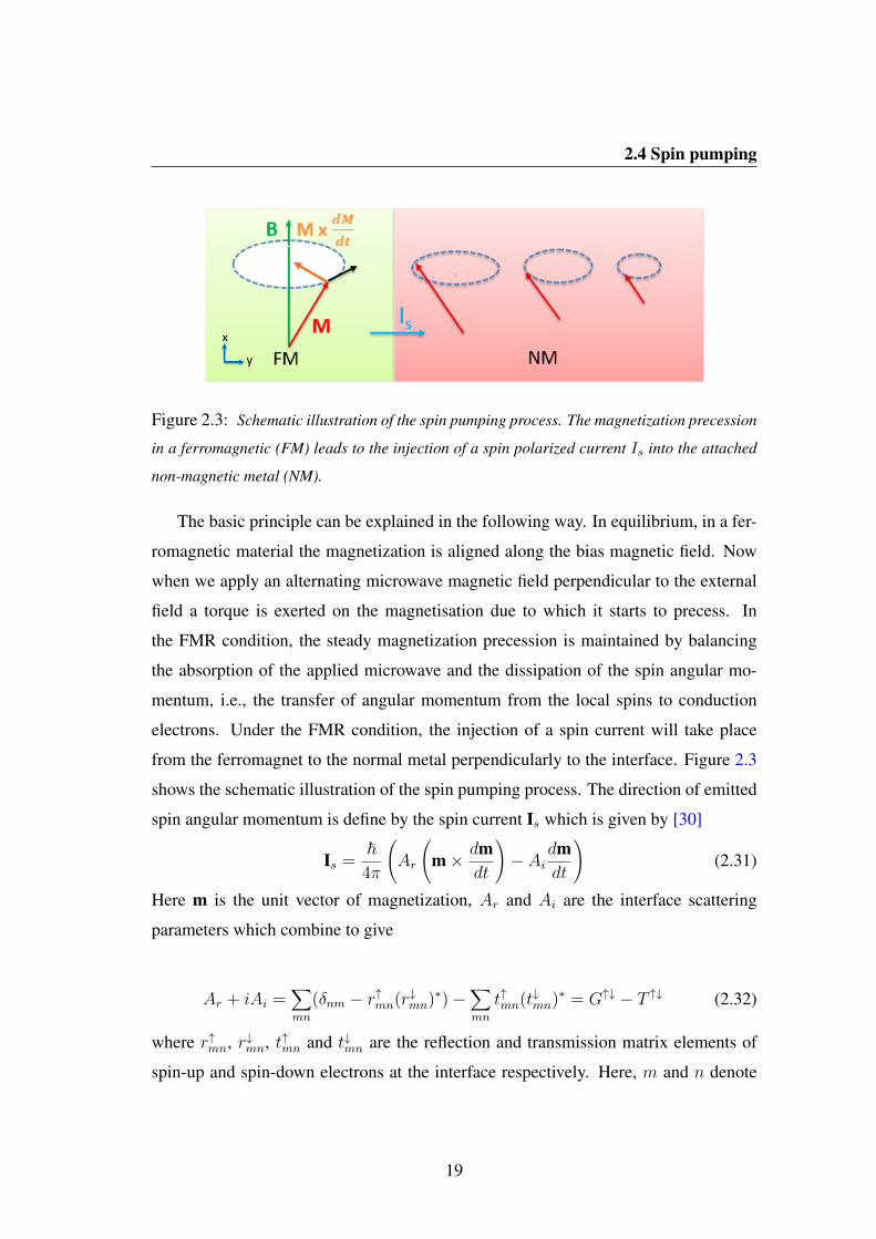
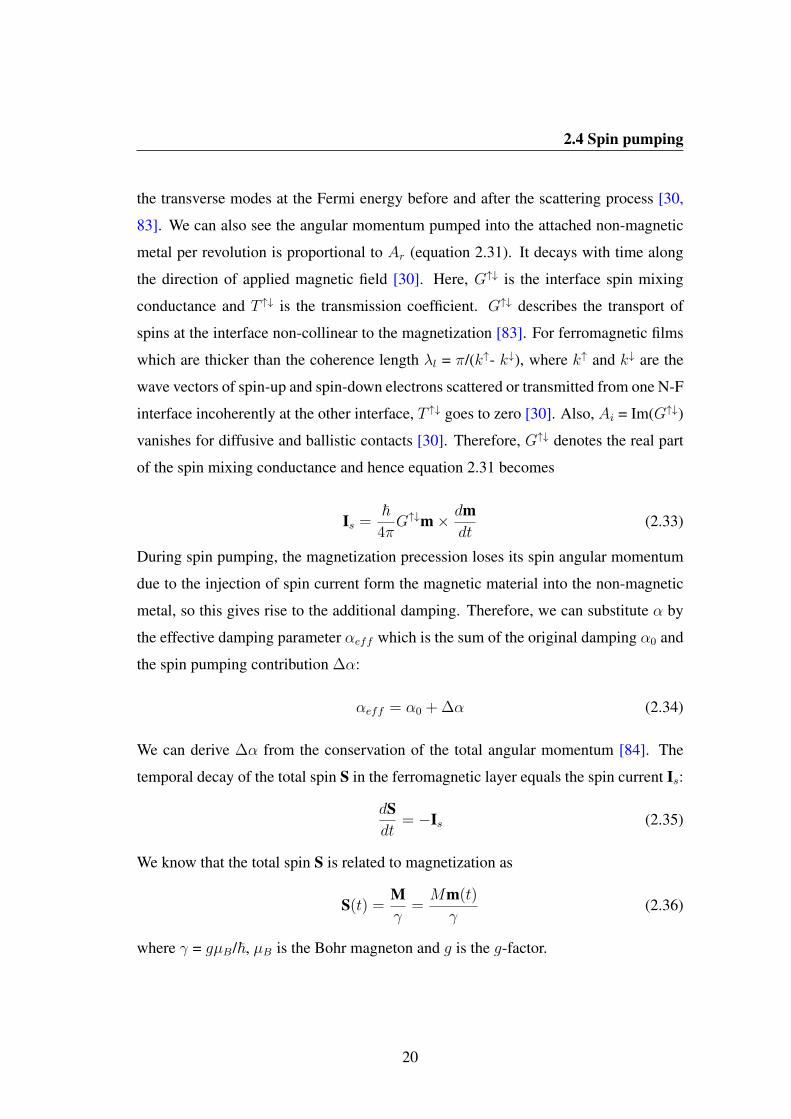
2.4 Spin pumping
Figure 2.3: Schematic illustration of the spin pumping process. The magnetization precession
in a ferromagnetic (FM) leads to the injection of a spin polarized current Is into the attached
non-magnetic metal (NM).
The basic principle can be explained in the following way. In equilibrium, in a fer-
romagnetic material the magnetization is aligned along the bias magnetic field. Now
when we apply an alternating microwave magnetic field perpendicular to the external
field a torque is exerted on the magnetisation due to which it starts to precess. In
the FMR condition, the steady magnetization precession is maintained by balancing
the absorption of the applied microwave and the dissipation of the spin angular mo-
mentum, i.e., the transfer of angular momentum from the local spins to conduction
electrons. Under the FMR condition, the injection of a spin current will take place
from the ferromagnet to the normal metal perpendicularly to the interface. Figure 2.3
shows the schematic illustration of the spin pumping process. The direction of emitted
spin angular momentum is define by the spin current Is which is given by [30]
Is = ~4π
(Ar
(m× dm
dt
)− Ai
dmdt
)(2.31)
Here m is the unit vector of magnetization, Ar and Ai are the interface scattering
parameters which combine to give
Ar + iAi =∑mn
(δnm − r↑mn(r↓mn)∗)−∑mn
t↑mn(t↓mn)∗ = G↑↓ − T ↑↓ (2.32)
where r↑mn, r↓mn, t↑mn and t↓mn are the reflection and transmission matrix elements of
spin-up and spin-down electrons at the interface respectively. Here, m and n denote
19
2.4 Spin pumping
the transverse modes at the Fermi energy before and after the scattering process [30,
83]. We can also see the angular momentum pumped into the attached non-magnetic
metal per revolution is proportional to Ar (equation 2.31). It decays with time along
the direction of applied magnetic field [30]. Here, G↑↓ is the interface spin mixing
conductance and T ↑↓ is the transmission coefficient. G↑↓ describes the transport of
spins at the interface non-collinear to the magnetization [83]. For ferromagnetic films
which are thicker than the coherence length λl = π/(k↑- k↓), where k↑ and k↓ are the
wave vectors of spin-up and spin-down electrons scattered or transmitted from one N-F
interface incoherently at the other interface, T ↑↓ goes to zero [30]. Also, Ai = Im(G↑↓)
vanishes for diffusive and ballistic contacts [30]. Therefore, G↑↓ denotes the real part
of the spin mixing conductance and hence equation 2.31 becomes
Is = ~4πG
↑↓m× dmdt
(2.33)
During spin pumping, the magnetization precession loses its spin angular momentum
due to the injection of spin current form the magnetic material into the non-magnetic
metal, so this gives rise to the additional damping. Therefore, we can substitute α by
the effective damping parameter αeff which is the sum of the original damping α0 and
the spin pumping contribution ∆α:
αeff = α0 + ∆α (2.34)
We can derive ∆α from the conservation of the total angular momentum [84]. The
temporal decay of the total spin S in the ferromagnetic layer equals the spin current Is:
dSdt
= −Is (2.35)
We know that the total spin S is related to magnetization as
S(t) = Mγ
= Mm(t)γ
(2.36)
where γ = gµB/~, µB is the Bohr magneton and g is the g-factor.
20

2.5 Current induced FMR
Thus it followsdmdt
= −gµB~M
dSdt
(2.37)
Equations (2.33) and (2.37) gives
dmdt
= ∆α(
m× dmdt
)(2.38)
with
∆α = gµBG↑↓
4πM (2.39)
Let us introduce g↑↓ = G↑↓/ A, where A is the interface area, then ∆α can be expressed
as
∆α = gµB4πMs
g↑↓
d(2.40)
where d is the thickness of magnetic layer and Ms is the saturation magnetisation per
unit volume. Hence, the effective Gilbert damping parameter is inversely proportional
to the thickness of the magnetic layer. In reference [85], dependence of spin pumping
effect on the thickness of YIG in YIG/Pt system has been reported. Also it has been
shown that with decrease in film thickness the linewidth and the effective damping
increases due to the magnetization relaxation through spin pumping in Pt.
2.5 Current induced FMR
Current induced FMR (CI-FMR) is a useful method to drive the magnetization dynam-
ics by the current induced spin transfer torque. It allows us to quantify the contribution
from the Oersted field and spin transfer torque in driving the magnetization dynam-
ics in YIG/Pt bilayer structure. An oscillating charge current at microwave frequency
flowing in a metal is accompanied by a transverse spin current Js due to the spin or-
bit interaction. This spin current also oscillates at the same frequency and can exert a
spin transfer torque (STT) on the magnetization M. This resonantly oscillating STT
can drive the magnetization precession at ferromagnetic resonance condition. The cur-
rent in the metal layer generates the Oersted field, can also drive the magnetization
21

2.5 Current induced FMR
precession. So, both the Oersted field and the spin current excites the magnetization
dynamics inside the magnetic layer and thus it is difficult to distinguish. The magnet-
ization dynamics are described by the Landau-Lifshitz-Gilbert equation, including the
spin transfer and Oersted field torques:
dMdt
= −γµ0M×Heff + α
Ms
(M× dM
dt
)+ γ~
2eMsdFJs (2.41)
where Heff is the effective magnetic field and α is the Gilbert damping parameter. Ms
and dF are the saturation magnetization per unit volume and thickness of the YIG film.
The magnetization dynamics can be detected electrically as a DC voltage generated
via spin pumping and the rectification mechanism of the spin Hall magnetoresistance
(SMR). From the lineshape and symmetry of the DC voltage we can understand the
nature of the torque acting on the system. Spin pumping is described as the symmetric
contribution to the Lorentzian lineshape whereas spin rectification consists of both
symmetric and anti-symmetric components in a Lorentzian curve. At the resonance
condition, the oscillating magnetization results in a time-dependent SMR in the metal
layer at the same frequency: R =R0 + ∆Rcos2θ(t), which rectifies the AC current and
generates a DC voltage along the bar. The spin rectification DC voltage is given by
[86]:
VDC = Vsym−SR∆H2
(Hext −Hres)2 + ∆H2 + Vasy−SR∆H(Hext −Hres)
(Hext −Hres)2 + ∆H2 (2.42)
where symmetric Vsym−SR and anti-symmetric Vasy−SR are Lorentzian components:
Vsym−SR = I0∆R2
√Hres(Hres +Meff )
∆H(2Hres +Meff )hST sin 2θ (2.43)
Vasy−SR = I0∆R2
(Hres +Meff )∆H(2Hres +Meff )
hOe sin 2θ cos θ (2.44)
where ∆H , Hext and Hres are the linewidth, external applied magnetic field and the
resonant field, respectively; θ is the angle between the applied field and the microwave
current I0ejwt andMeff is the effective magnetization. Thus, Oersted field hOe induces
anti-symmetric components Vasy−SR and the Vsym−SR is induced by the out-of-plane
22

2.6 Spin current and Spin diffusion
field hST which is responsible for an anti-damping like spin transfer torque. Figure
2.4 shows the schematic of CI-FMR in YIG/Pt bilayer sample with its measurement
circuit.
a
Figure 2.4: Schematic of a YIG/Pt bilayer thin film illustrating the spin transfer torque τST
and the Oersted field torque τOe driving the magnetization precession about the external field
Hext. It is also showing the circuit for CI-FMR measurement where a bias-Tee is used for
the transmission of a microwave signal and dc voltage detection simultaneously, via lock-in
technique across the Pt bar [86].
Schreier et al. reported the experiment on in-plane CI-FMR in YIG/Pt, in which
they found the magnetization dynamics in thinnest YIG sample (4 nm) is driven by
the spin transfer torque [87]. Researchers also reported the direct imaging of electric-
ally driven spin-torque FMR (ST-FMR) in YIG by spatially-resolved Brillouin light
scattering (BLS) spectroscopy [88]. In our work, we used CI-FMR to drive the mag-
netization dynamics in YIG/Pt layer with YIG of varying thickness and to investigate
the contribution from the Oersted field and spin-transfer torque.
2.6 Spin current and Spin diffusion
An electron has an internal angular momentum. This angular momentum is due to the
spin of the electron. The flow of spin is called a spin current. This plays the similar role
as the flow of charge in an electrical current. A charge current is defined in terms of the
23
2.6 Spin current and Spin diffusion
charge conservation law. The continuity equation of charge, which is a representation
of the charge conservation law, defines a charge current density jc [89]:
ρ = −∇ · jc (2.45)
However, spin is not conserved completely due to the spin relaxation and it obeys the
continuity equation [90]:dMdt
= −∇ · js + T (2.46)
The term T represents the nonconservation of spin angular momentum due to the relax-
ation and generation of spin angular momentum. Here M denotes the magnetisation
and js is the spin current density. The basic phenomenological model for the spin
relaxation can be defined as [90]:
T = −(M−M0)/τ (2.47)
wher τ is a decay time constant and (M −M0) is the nonequilibrium magnetization
measured from equilibrium value M0.
In a ferromagnet/normal metal bilayer structure, a spin current can be injected from
a ferromagnet (FM) into a normal metal (NM). Figure 2.5 shows a spin current in a
FM/NM junction with a charge current passing through the interface. For a diffusion or
drift spin current the driving force is a gradient of the difference in the spin dependent
electrochemical potential for spin up (µ↑) and spin down (µ↓). With this the charge
current density jc and spin current density js can be written as [90]:
jc = j↑ + j↓ = 1e
∇(σ↑µ↑ + σ↓µ↓) (2.48)
js = j↑ − j↓ = 1e
∇(σ↑µ↑ − σ↓µ↓) (2.49)
where σ↑ and σ↓ represents the spin up and spin down conductivity respectively.
The continuity equations for charge and spin in the steady state are
∇.(j↑ + j↓) = 0 (2.50)
24

2.6 Spin current and Spin diffusion
∇.(j↑ − j↓) = −eδn↑τ↑↓
+ eδn↓τ↓↑
(2.51)
where δn↑(↓) is the deviation from equilibrium carrier density for spin up (spin down),
and τ↑↓ is the scattering time of an electron from spin state ↑ to ↓ or vice-versa. Using
the continuity equations and balance principle N↑τ↑↓
= N↓τ↓↑
, which means that in equilib-
rium there is no net spin scattering, we obtain the basic equations that describe the
charge and spin transport as [90]:
∇2(σ↑µ↑ + σ↓µ↓) = 0 (2.52)
∇2(µ↑ − µ↓) = 1λ2sd
(µ↑ − µ↓) (2.53)
Equation 2.53 is known as the spin diffusion equation. Here, λsd =√Dτsf is the spin
diffusion length, D is the spin-averaged diffusion constant and τsf is the spin relaxation
time.
Figure 2.5: Spatial variation of the spin dependent electrochemical potentials across a cur-
rent carrying interface at an ferromagnet/normal metal (FM/NM) junction. The decay of spin
accumulation away from the interface is characterised by the spin diffusion lengths LsF and
LsN in the FM and NM regions, respectively [91].
In a FM/NM junctions, when a spin polarised current passes into the normal metal
the chemical potentials for the spin up and spin down diverge over a short range, over
which spin accumulation occurs in the NM. In nonmagnetic metals, the electrical con-
ductivity is spin-independent, and the charge current has no spin polarisation. So the
25

2.7 Spin Hall effect and inverse spin Hall effect
non-conservation of spin current takes place over a spatial axis defined by the spin dif-
fusion length. As the conduction electrons move into the NM the chemical potentials
have to be continuous but due to the interface contact resistance there can be a small
difference. The gap between the dashed lines ∆µ is called the spin accumulation. The
spin accumulation (µ↑ - µ↓) decay away from the interface into the FM and NM re-
gions. In the NM, this spin accumulation decays over a spin diffusion length LsN . In
the FM near the interface there is a back flow of spin polarised electrons over a distance
LsF , induced by the accumulation in the NM.
2.7 Spin Hall effect and inverse spin Hall effect
The spin Hall effect (SHE) is the generation of transverse spin current by an electric
charge current with spins oriented perpendicular to the two currents [92]. Electrons
with spin up will be scattered in one direction perpendicular to the flow of the electric
charge current and electrons with spin down in the opposite direction (figure 2.6a).
It does not require any magnetic field. This effect was first predicted theoretically in
1971 by D′yakonov and Perel [93, 94]. But this theoretical work received the attention
of the spintronics community when it was rediscovered by Hirsch [32] and Zhang [34]
in 1999. The reverse effect is the inverse spin Hall effect (ISHE) which describes the
generation of a transverse electric charge current in a normal metal by the injection of
a spin polarised current (figure 2.6b). Experimentalists have been able to measure and
quantitatively study the spin Hall effect and its inverse in a variety of systems, such as
in semiconductors like ZnSe [95] and GaAs [96–98], and metals, for example, Al [99]
and Pt [100, 101].
SHE is a consequence of spin orbit interactions [102]. The expression for the spin-
orbit interaction in vacuum is [103]:
HSO = −λ20
4~ [p×∇V (r)].σ (2.54)
where λ0 = ~/mc ' 3.9 x 10⁻³A is the Compton wavelength of the electron divided
26
2.7 Spin Hall effect and inverse spin Hall effect
by 2π, p is the momentum, V (r) is the potential acting on the electron and σ is the
vector of the Pauli matrices. Traditionally this form is explained as the relativistic
transformation of the electric field∇V to the rest frame of the electron [103]. In solids,
the impurity potential gives rise to an additional electric field due to which an electron
passing through this field feels an effective magnetic field. This leads to spin-orbit
coupling
HSO(k) = −12σ.B(k) (2.55)
where B(k) is an effective k-dependent magnetic field for the electron band considered.
This results in a spin dependent perturbation on the conduction electron momentum.
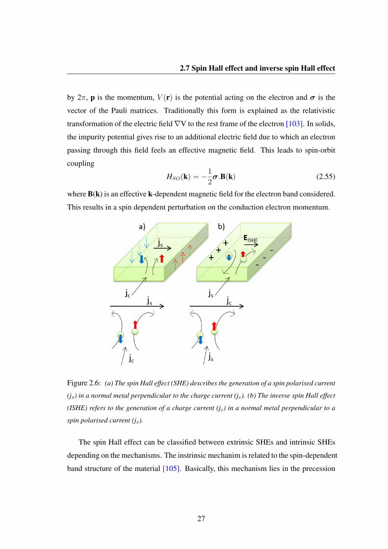
Figure 2.6: (a) The spin Hall effect (SHE) describes the generation of a spin polarised current
(js) in a normal metal perpendicular to the charge current (jc). (b) The inverse spin Hall effect
(ISHE) refers to the generation of a charge current (jc) in a normal metal perpendicular to a
spin polarised current (js).
The spin Hall effect can be classified between extrinsic SHEs and intrinsic SHEs
depending on the mechanisms. The instrinsic mechanim is related to the spin-dependent
band structure of the material [105]. Basically, this mechanism lies in the precession
27
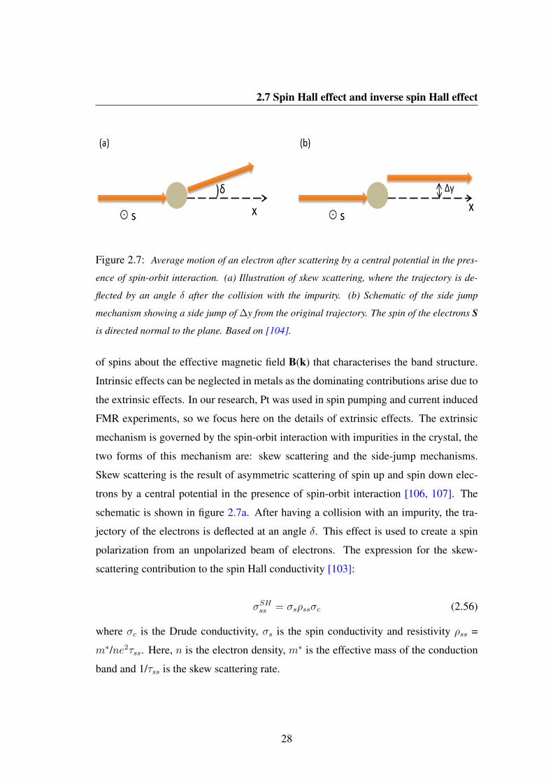
2.7 Spin Hall effect and inverse spin Hall effect
Figure 2.7: Average motion of an electron after scattering by a central potential in the pres-
ence of spin-orbit interaction. (a) Illustration of skew scattering, where the trajectory is de-
flected by an angle δ after the collision with the impurity. (b) Schematic of the side jump
mechanism showing a side jump of ∆y from the original trajectory. The spin of the electrons S
is directed normal to the plane. Based on [104].
of spins about the effective magnetic field B(k) that characterises the band structure.
Intrinsic effects can be neglected in metals as the dominating contributions arise due to
the extrinsic effects. In our research, Pt was used in spin pumping and current induced
FMR experiments, so we focus here on the details of extrinsic effects. The extrinsic
mechanism is governed by the spin-orbit interaction with impurities in the crystal, the
two forms of this mechanism are: skew scattering and the side-jump mechanisms.
Skew scattering is the result of asymmetric scattering of spin up and spin down elec-
trons by a central potential in the presence of spin-orbit interaction [106, 107]. The
schematic is shown in figure 2.7a. After having a collision with an impurity, the tra-
jectory of the electrons is deflected at an angle δ. This effect is used to create a spin
polarization from an unpolarized beam of electrons. The expression for the skew-
scattering contribution to the spin Hall conductivity [103]:
σSHss = σsρssσc (2.56)
where σc is the Drude conductivity, σs is the spin conductivity and resistivity ρss =
m∗/ne2τss. Here, n is the electron density, m∗ is the effective mass of the conduction
band and 1/τss is the skew scattering rate.
28

2.7 Spin Hall effect and inverse spin Hall effect
The side-jump mechanism originates from the anomalous form of the velocity op-
erator in spin-orbit coupled systems [104, 108]. It is regarded as a discontinuous finite
displacement of an electron (represented by a wave packet) transverse to the original
direction. This effect arises due to random collisions of electrons with impurities. The
jump is not necessarily transverse to the incident wave direction as it can happen in all
possible directions. Since the displacement is the same for spin up and spin down elec-
trons but in opposite directions, a spin current perpendicular to the initially unpolarised
charge current is generated. The side-jump contribution to the spin Hall conductivity
is given by [103]:
σSHsj = −2e2
~nλ2
c (2.57)
where λc is the coupling constant of the conduction band and n is the electron density.
Thus, the spin Hall conductivity is expressed as the sum of two contributions: σSH =
σSHss + σSHsj .
The spin Hall resistivity ρH has a linear and a quadratic term in the electric res-
istivity ρ [109]:
ρH = askewρ+ bsideρ2 (2.58)
where askew and bside are temperature dependent parameters which describes the skew
scattering and side jump contribution, respectively.
The spin current density js and charge current density jc are coupled by the follow-
ing equations [109]:
jc = j0c + θSHE
2e~
(js × σ) (2.59)
js = j0s + θSHE
2e~
(jc × σ) (2.60)
where j0c and j0
s are the original current densities, θSHE is the spin Hall angle and σ is
the spin polarization vector. The spin Hall angle θSHE is a material parameter and it is
the sum of the contribution from skew scattering and side jump scattering mechanisms.
The measure of spin Hall effect is given by the spin Hall angle θSHE , which is defined
as the ratio of the spin conductivity and the electrical conductivity. From equation 2.59
29
2.7 Spin Hall effect and inverse spin Hall effect
and 2.60, it appears that a spin current induces a transverse charge current, while a
charge current generates a transverse spin current.
The spin current injected into the non-magnetic metal layer decays along the y-axis
(fig.2.3) due to spin relaxation as [110]:
js(y) =sinhdN−y
λsd
sinh dN
λsd
j0s (2.61)
where dN is the normal metal thickness, λsd is the spin-diffusion length and j0s is
the spin-current density at the interface. The spin pumping induced spin current is
transformed into charge current by ISHE. Here j0c is zero, so eq. 2.59 becomes
jc = θSHE2e~
(js × σ) (2.62)
Substituting js using equation 2.61 in eq. 2.62 and averaging over the Pt thickness
yields the average current density which is given by [110]:
jc = 1dPt
∫ dP t
0jc(y)dy = θSHE
2e~λsddPt
tanh(dpt
2λsd
)j0s (2.63)
where dPt is the thickness of the Pt and λsd is the spin diffusion length. With A as the
cross-sectional area of the Pt layer, the ISHE charge current is given by IISHE = A jc.
Hence, the ISHE voltage is EISHE = IISHER, where R is the electrical resistance of
the Pt layer.
30
CHAPTER 3
Experimental Methods
31
3.1 Introduction
3.1 Introduction
This chapter starts with the introduction of deposition technique of nanometre thick
Yttrium iron garnet films and various experimental techniques employed for the char-
acterisation of thin films of YIG. The first section will address the deposition of YIG
by RF magnetron sputtering and the process of growing YIG/Pt and YIG/C60 bilayer
structures. The structural characterisation of thin YIG films involves x-ray reflectivity
(XRR) and x-ray diffraction (XRD) in order to determine the thickness, crystallin-
ity and the film quality. The surface roughness of the films was determined using
atomic force microscopy (AFM). The magnetic properties of the films are analysed
using vibrating sample magnetometer (VSM) and superconducting quantum interfer-
ence devices (SQUID) VSM. For detailed investigation of the magnetization behaviour
at low temperature, we further carried out a temperature dependent polarised neutron
reflectometry (PNR) experiment. We also used Ferromagnetic resonance (FMR) tech-
niques to investigate the magnetization dynamics of our films and hence to estimate
the value of damping parameter in our nm-thick sputtered YIG films.
3.2 Deposition: DC and RF sputtering
Sputtering is a physical vapour deposition of thin films on the substrates. This tech-
nique belongs to the category of plasma deposition. In this process, sputtered gas is
ionized electrically to form a plasma, followed by removal of the target material by
ion bombardment and ejection of material from the target to the substrate. The main
advantages of sputtering are: (a) High deposition rate for DC sputtering. (b) Film
uniformity over large areas. (c) Surface smoothness and thickness control. (d) It is a
versatile process as it is based on the momentum transfer and not on thermal or chem-
ical reaction, so any kind of material can be sputtered.
The sputtering deposition chamber consists of two electrodes in a vacuum with an
external high voltage power supply. The material to be deposited, is called the target
32
3.2 Deposition: DC and RF sputtering
and acts as the cathode, the substrates are placed on the sample wheel which is earthed.
A schematic diagram of a sputtering system is shown in 3.1. The sputtering gas is
introduced into the vacuum chamber. To sputter an atom from the target, momentum
transfer from the ion-induced collision must overcome the surface barrier, given by the
surface binding energy. When a voltage is applied between the cathode and anode,
an electric discharge is produced. This leads to the partial ionization of the gas and
these ions when strike the target with sufficient energy cause ejection of surface atoms
from the target and deposition onto the substrate. During this the ionized gas and the
free electrons are accelerated by the voltage and continue to collide, causing further
ionization of the gas. Finally, a breakdown condition is reached and the plasma is
stabilized. The principal source of electrons to sustain the plasma is the secondary
electron emission. Sputter Yield gives a measure of ejected surface atoms, and is
defined as the ratio between the mean number of ejected atoms from the surface and
the number of incident ions bombarding the target. The sputter yield is influenced by
the following factors [111]: (a) energy of incident particles (b) the atomic weights of
the ion and the target atom (c) incident angles of particles (d) crystal structure of the
target surface. The sputter yield shows maximum value in a high-energy region of 10
to 100 keV. The high yield is observed at incident angles between 60 - 80 [111].
Sputtering methods can be classified as DC and RF sputtering depending on the
material to be deposited. DC sputtering is used for the metal deposition whereas RF
sputtering for the deposition of thin films of insulator. In DC sputtering, a DC voltage
(∼ 400 V) is applied to create plasma between the electrodes. In RF sputtering, a
voltage oscillating at radio frequency (RF), typically around 13.56 MHz, is applied
to bias the electrode and to sustain the glow discharge. As the current is alternating,
this will prevent build up of a surface charge of positive ions on the front side of
the insulator. On the positive cycle, electrons are attracted to the cathode, creating a
negative bias and on the negative cycle, ion bombardment of the target to be sputtered
continues. The sputtered atoms are ejected, which are then deposited on the substrate.
For magnetron sputtering, permanent magnets are placed beneath the target so as to
33
3.2 Deposition: DC and RF sputtering
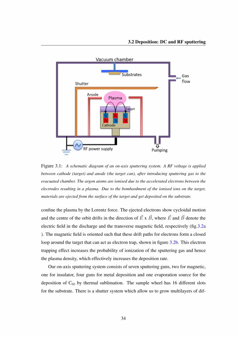
Figure 3.1: A schematic diagram of an on-axis sputtering system. A RF voltage is applied
between cathode (target) and anode (the target can), after introducing sputtering gas to the
evacuated chamber. The argon atoms are ionised due to the accelerated electrons between the
electrodes resulting in a plasma. Due to the bombardment of the ionised ions on the target,
materials are ejected from the surface of the target and get deposited on the substrate.
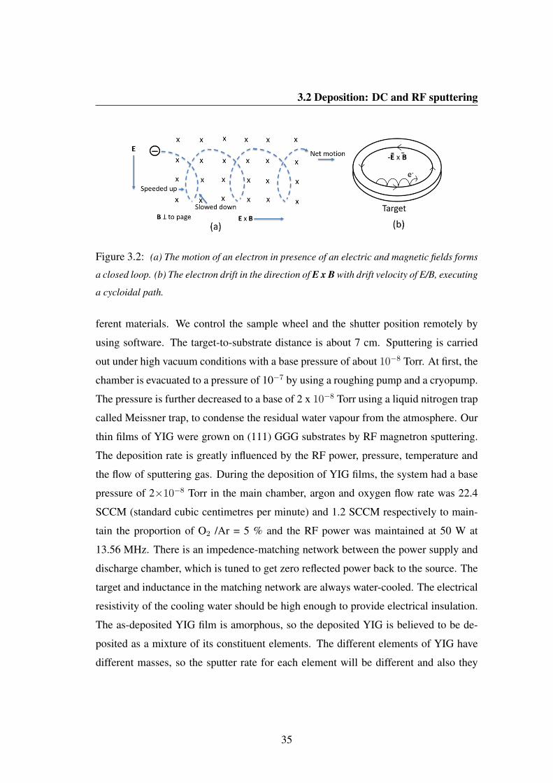
confine the plasma by the Lorentz force. The ejected electrons show cycloidal motion
and the centre of the orbit drifts in the direction of ~E x ~B, where ~E and ~B denote the
electric field in the discharge and the transverse magnetic field, respectively (fig.3.2a
). The magnetic field is oriented such that these drift paths for electrons form a closed
loop around the target that can act as electron trap, shown in figure 3.2b. This electron
trapping effect increases the probability of ionization of the sputtering gas and hence
the plasma density, which effectively increases the deposition rate.
Our on-axis sputtering system consists of seven sputtering guns, two for magnetic,
one for insulator, four guns for metal deposition and one evaporation source for the
deposition of C60 by thermal sublimation. The sample wheel has 16 different slots
for the substrate. There is a shutter system which allow us to grow multilayers of dif-
34
3.2 Deposition: DC and RF sputtering
Figure 3.2: (a) The motion of an electron in presence of an electric and magnetic fields forms
a closed loop. (b) The electron drift in the direction of E x B with drift velocity of E/B, executing
a cycloidal path.
ferent materials. We control the sample wheel and the shutter position remotely by
using software. The target-to-substrate distance is about 7 cm. Sputtering is carried
out under high vacuum conditions with a base pressure of about 10−8 Torr. At first, the
chamber is evacuated to a pressure of 10−7 by using a roughing pump and a cryopump.
The pressure is further decreased to a base of 2 x 10⁻⁸ Torr using a liquid nitrogen trap
called Meissner trap, to condense the residual water vapour from the atmosphere. Our
thin films of YIG were grown on (111) GGG substrates by RF magnetron sputtering.
The deposition rate is greatly influenced by the RF power, pressure, temperature and
the flow of sputtering gas. During the deposition of YIG films, the system had a base
pressure of 2×10⁻⁸ Torr in the main chamber, argon and oxygen flow rate was 22.4
SCCM (standard cubic centimetres per minute) and 1.2 SCCM respectively to main-
tain the proportion of O2 /Ar = 5 % and the RF power was maintained at 50 W at
13.56 MHz. There is an impedence-matching network between the power supply and
discharge chamber, which is tuned to get zero reflected power back to the source. The
target and inductance in the matching network are always water-cooled. The electrical
resistivity of the cooling water should be high enough to provide electrical insulation.
The as-deposited YIG film is amorphous, so the deposited YIG is believed to be de-
posited as a mixture of its constituent elements. The different elements of YIG have
different masses, so the sputter rate for each element will be different and also they
35
3.3 Annealing
will have different mean free path. By adding oxygen to the argon atmosphere, we
slow down the growth rate and allow the yttrium and iron to be deposited as the correct
stoichiometry for YIG. The deposition rate used was 0.29 A/s (Old Target: Target-A).
The rate was determined from the thickness of each sample obtained after fitting the
x-ray reflectivity curve. Under this deposition condition thin films of YIG of vary-
ing thicknesses were deposited on GGG. Later, with the change to a new YIG target
(Target-B), the rate was around 0.16 A/s under the same deposition conditions.
For YIG/C60 bilayer structures, C60 molecules were deposited on annealed YIG by
thermal sublimation. The C60 molecules are placed in a crucible in powder form and
the crucible is connected to a tungsten filament. When a high current about 20.8 A
is applied to the copper rods attached to the tungsten filament, the temperature of the
crucible rises and due to this high temperature the molecules are thermally sublimated
and deposited on the YIG surface. A water cooling system is arranged with the evap-
oration source to avoid excessive radiative heating. During the growth of C60, a quartz
crystal monitor is used to determine the thickness of the C60 layer. After each growth,
thickness is measured and the tooling factor of the monitor is calibrated accordingly
so as to get the accurate thickness of C60 layer.
Our YIG/Pt bilayer samples are made by deposition of Pt by DC magnetron sput-
tering on annealed YIG samples. Before deposition of Pt the samples are cleaned in
ultrasonic bath using acetone and isopropanol. The deposition rate of Pt was 1.65 A/s
at 25 mA with power of 9 W.
3.3 Annealing
The as-deposited YIG films are amorphous and non-magnetic, so it is required to an-
neal them to get crystalline YIG along the GGG crystalline plane. For annealing, the
samples are first cleaned using acetone and isopropanol. Then the samples are imme-
diately placed in a tube furnace to anneal them at 850 C for two hours under open air
conditions. Care was taken to keep the samples within a 15 cm region in the centre
36
3.4 Structural Characterisation
of the furnace where the temperature was approximately uniform. The heating and
cooling cycles are run at a rate of 7C per minute to avoid strain on the films. For the
deposition of Pt and C60 on YIG, the samples need to be reloaded into the sputtering
chamber after annealing.
3.4 Structural Characterisation
3.4.1 X-ray reflectivity (XRR)
X-ray reflectivity is a useful and non-destructive technique for the structural charac-
terisation of thin films. This technique is used to determine the thin film parameters:
thickness, density and surface or interface roughness. When x-rays are incident on the
sample, the refractive index of the material n is slightly less than one, given by
n = 1− δ (3.1)
where δ = 2πρr0k2 . Here, ρ, r0 and k are the electron density, Bohr radius and wave
vector of the radiation, respectively. δ is the order of 10−5. When x-rays are incident
on a sample at a grazing angle lower than the critical angle of incidence θc, they un-
dergo total reflection and do not enter the sample. When the angle of incidence θ>θc ,
refraction occurs and x-rays penetrate in the material.
Snell’s law of refraction gives the relationship between the angle of incidence θ
and angle of refraction θ′ which is given by
cos θ = n cos θ′(3.2)
The critical angle can be derived from the Snell’s law by putting θ′= θc and expanding
the cosine in Snell’s law to give the expression for critical angle. The critical angle of
incidence θc is given by the formula:
θc =√
2δ =√
4πρr0
k2 (3.3)
37

3.4 Structural Characterisation
Thus, the critical angle provides the information about electron density of the reflecting
material [112, 113].
The reflectivity is measured at grazing incidence including the straight-through
beam such that the region below ∼ 0.4 is due to the instrument function i.e. the
beam optics. This is immediately followed by a sharp decrease in the intensity at the
critical angle: the point where the beam just penetrates the top surface. The reflected
profile shows oscillations caused by the interference of x-rays reflected from the sur-
face of the film and the interface between the film and the substrate. These oscillations
are known as Kiessig fringes [114]. By analysing the reflectivity intensity curves we
can determine the thickness, density, surface and interface roughness of the thin films.
The quality of the fit gives us confidence that the top layer is stoichiometrically correct
(section 4.2.1). The amplitude of oscillations depends on the difference in the densities
of the film and the substrate. The higher the amplitude of oscillations larger the differ-
ence. So the amplitude of oscillations and the critical angle provide information about
the density of film. From the decay rate of reflectivity, we can determine the roughness
of the film. For a larger surface roughness reflectivity decreases rapidly, so larger the
surface roughness, the faster the decay of oscillations. The angular positions of oscil-
lation give information about the thickness of the film. The thickness of the film, t,
can be determined by analysing the angular distributions of the resulting interference
pattern using the Kiessig equation:
λ = 2t√
sin2 θn − sin2 θc (3.4)
where n is an integer, λ is the wavelength and θn is the angular position of constructive
peaks [113, 115].
3.4.2 X-ray diffraction (XRD)
X-ray diffraction is a technique used for the determination of the crystal structure of
the material. This technique is based on the coherent interference of scattered waves
38
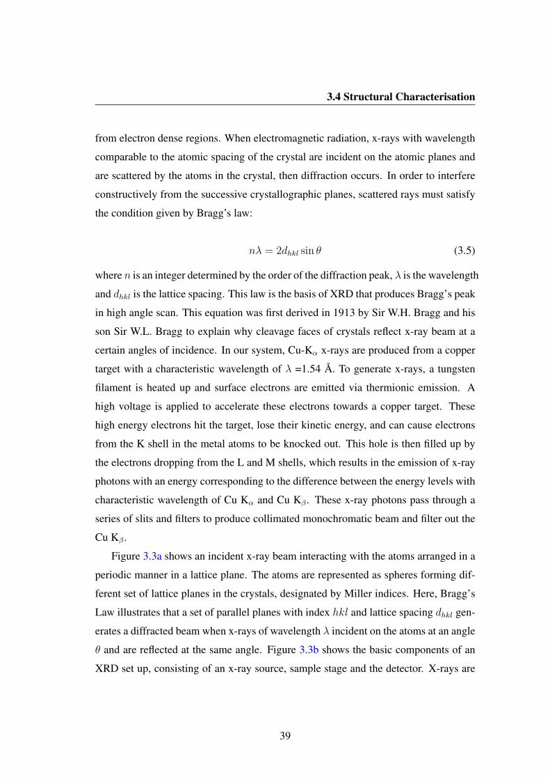
3.4 Structural Characterisation
from electron dense regions. When electromagnetic radiation, x-rays with wavelength
comparable to the atomic spacing of the crystal are incident on the atomic planes and
are scattered by the atoms in the crystal, then diffraction occurs. In order to interfere
constructively from the successive crystallographic planes, scattered rays must satisfy
the condition given by Bragg’s law:
nλ = 2dhkl sin θ (3.5)
where n is an integer determined by the order of the diffraction peak, λ is the wavelength
and dhkl is the lattice spacing. This law is the basis of XRD that produces Bragg’s peak
in high angle scan. This equation was first derived in 1913 by Sir W.H. Bragg and his
son Sir W.L. Bragg to explain why cleavage faces of crystals reflect x-ray beam at a
certain angles of incidence. In our system, Cu-Kα x-rays are produced from a copper
target with a characteristic wavelength of λ =1.54 A. To generate x-rays, a tungsten
filament is heated up and surface electrons are emitted via thermionic emission. A
high voltage is applied to accelerate these electrons towards a copper target. These
high energy electrons hit the target, lose their kinetic energy, and can cause electrons
from the K shell in the metal atoms to be knocked out. This hole is then filled up by
the electrons dropping from the L and M shells, which results in the emission of x-ray
photons with an energy corresponding to the difference between the energy levels with
characteristic wavelength of Cu Kα and Cu Kβ . These x-ray photons pass through a
series of slits and filters to produce collimated monochromatic beam and filter out the
Cu Kβ .
Figure 3.3a shows an incident x-ray beam interacting with the atoms arranged in a
periodic manner in a lattice plane. The atoms are represented as spheres forming dif-
ferent set of lattice planes in the crystals, designated by Miller indices. Here, Bragg’s
Law illustrates that a set of parallel planes with index hkl and lattice spacing dhkl gen-
erates a diffracted beam when x-rays of wavelength λ incident on the atoms at an angle
θ and are reflected at the same angle. Figure 3.3b shows the basic components of an
XRD set up, consisting of an x-ray source, sample stage and the detector. X-rays are
39
3.5 Magnetometry
Figure 3.3: (a) Bragg conditions for X-ray diffraction from atomic planes in the crystal. The
incident waves are reflected by the crystal planes. The diffracted waves will be in phase when
the Bragg’s Law, nλ = 2d sin θ is satisfied. (b) Schematic of x-ray diffraction (XRD) set up. Its
basic components are x-ray source, a sample stage and a detector.
incident on the sample at an angle θ and reflected x-rays are detected by a movable
detector at angle 2θ. To measure at specular condition, the detector moves double the
angle the sample moves. Measurements were carried out by varying the angle of in-
cidence and the corresponding intensities of the diffracted peaks produce a diffraction
pattern.
3.5 Magnetometry
3.5.1 Vibrating sample magnetometer
A vibrating sample magnetometer (VSM) is a device used to measure the magnetic
moment of magnetic thin films. It operates on Faraday’s Law of Induction, which tells
us that a change in magnetic flux will produce an induced electromotive force (EMF)
in a coil and this electric field gives the information about the changing magnetic mo-
ment. The sample to be studied is kept in a magnetic field. If the sample is magnetic,
40

3.5 Magnetometry
this magnetic field will magnetize the sample by aligning the magnetic domains, or
the individual spins, with the field. The magnetic dipole moment of the sample will
then create a magnetic field around the sample, called the magnetic stray field. As
the sample is vibrated at a known frequency, this magnetic stray field changes as a
function of time. This alternating magnetic field will then produce an electric current
in the pick-up coils according to Faraday’s Law of Induction. This current will be
proportional to the moment of the sample.
Figure 3.4: Schematic of a vibrating sample magnetometer. Samples are vibrated in presence
of an applied magnetic field. Induced voltage in the two coils is measured which are wound in
opposite directions to reduce any background interference [116].
Our Oxford Instruments Maglab VSM provides temperature control over a range of
1.5 K to 305 K. Figure 3.4 shows the schematic of a vibrating sample magnetometer.
The sample is mounted on a Polyether etherketone (PEEK) paddle. This paddle is
then attached to a carbon-fibre rod and inserted into a helium flow cryostat where the
sample is held between two pick-up coils. This rod is placed in a variable temperature
insert (VTI) surrounded by a liquid helium bath. The liquid helium is surrounded
by a nitrogen reservoir and separated by a vacuum jacket. Temperature control is
41
3.5 Magnetometry
maintained by the flow of liquid helium, fed into the VTI by a small helium inlet
(needle valve) and a DC resistance heater located at the base of the VTI. The pressure
inside the VTI is constantly maintained by a roughing pump. The sample is then
vibrated in presence of an applied magnetic field which will magnetise the sample.
Through the superconducting magnet surrounding the sample chamber we can apply a
magnetic field up to 9 T parallel to the rod. The sample vibrates at 55 Hz as determined
by the lock-in connected to a vibrator at the top of the VTI. As the sample vibrates,
this results in a change in magnetic flux through the coils that induces an EMF. Current
generated in the pick-up coils due to the change in flux at the driving frequency was
amplified and interpreted by the lock-in amplifier.
Care must be taken for any background signal from substrates and the probe that
can interfere with the small useful signal from thin magnetic films. We should pre-
pare our samples in a clean environment to avoid surface contamination by magnetic
impurities.
3.5.2 Superconducting quantum interference device
The superconducting quantum interference device (SQUID) is the most attractive mag-
netic sensor to measure very small magnetic moments with high sensitivity. It is based
on quantum effects in superconducting loops. A Josephson junction is the heart of
squid technology in which current flows between two superconductors separated by
a thin insulator through quantum tunnelling. A Josephson junction is a small gap
between two superconductors through which Cooper pairs can tunnel. A squid con-
sists of a single (rf squid) or double (dc squid) Josephson junctions in a superconduct-
ing loop. Figure 3.5 shows the schematic of a Josephson junction.
In the Josephson equation, the supercurrent Is passing through the junction is re-
lated to the relative phase difference δ across the junction and the critical current of the
junction, I0 as
Is = I0 sin δ, δ = θ1 − θ2 (3.6)
42
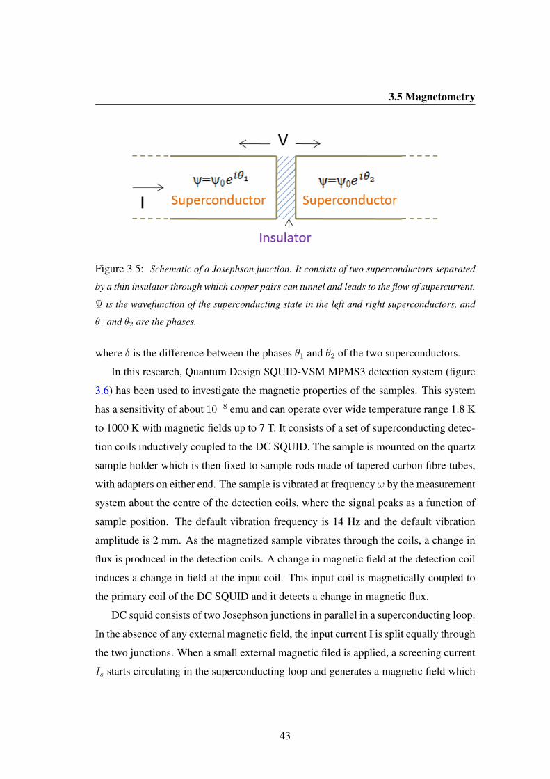
3.5 Magnetometry
Figure 3.5: Schematic of a Josephson junction. It consists of two superconductors separated
by a thin insulator through which cooper pairs can tunnel and leads to the flow of supercurrent.
Ψ is the wavefunction of the superconducting state in the left and right superconductors, and
θ1 and θ2 are the phases.
where δ is the difference between the phases θ1 and θ2 of the two superconductors.
In this research, Quantum Design SQUID-VSM MPMS3 detection system (figure
3.6) has been used to investigate the magnetic properties of the samples. This system
has a sensitivity of about 10−8 emu and can operate over wide temperature range 1.8 K
to 1000 K with magnetic fields up to 7 T. It consists of a set of superconducting detec-
tion coils inductively coupled to the DC SQUID. The sample is mounted on the quartz
sample holder which is then fixed to sample rods made of tapered carbon fibre tubes,
with adapters on either end. The sample is vibrated at frequency ω by the measurement
system about the centre of the detection coils, where the signal peaks as a function of
sample position. The default vibration frequency is 14 Hz and the default vibration
amplitude is 2 mm. As the magnetized sample vibrates through the coils, a change in
flux is produced in the detection coils. A change in magnetic field at the detection coil
induces a change in field at the input coil. This input coil is magnetically coupled to
the primary coil of the DC SQUID and it detects a change in magnetic flux.
DC squid consists of two Josephson junctions in parallel in a superconducting loop.
In the absence of any external magnetic field, the input current I is split equally through
the two junctions. When a small external magnetic filed is applied, a screening current
Is starts circulating in the superconducting loop and generates a magnetic field which
43
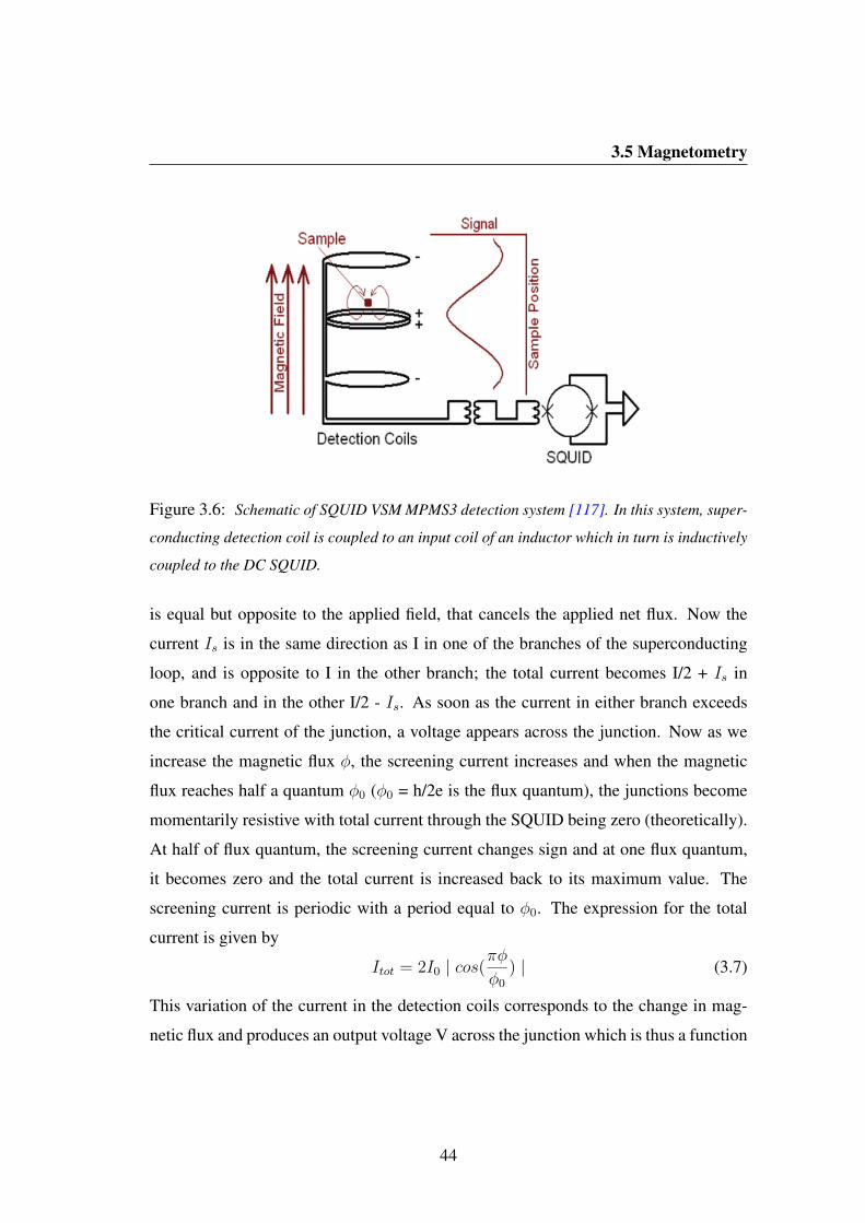
3.5 Magnetometry
Figure 3.6: Schematic of SQUID VSM MPMS3 detection system [117]. In this system, super-
conducting detection coil is coupled to an input coil of an inductor which in turn is inductively
coupled to the DC SQUID.
is equal but opposite to the applied field, that cancels the applied net flux. Now the
current Is is in the same direction as I in one of the branches of the superconducting
loop, and is opposite to I in the other branch; the total current becomes I/2 + Is in
one branch and in the other I/2 - Is. As soon as the current in either branch exceeds
the critical current of the junction, a voltage appears across the junction. Now as we
increase the magnetic flux φ, the screening current increases and when the magnetic
flux reaches half a quantum φ0 (φ0 = h/2e is the flux quantum), the junctions become
momentarily resistive with total current through the SQUID being zero (theoretically).
At half of flux quantum, the screening current changes sign and at one flux quantum,
it becomes zero and the total current is increased back to its maximum value. The
screening current is periodic with a period equal to φ0. The expression for the total
current is given by
Itot = 2I0 | cos(πφ
φ0) | (3.7)
This variation of the current in the detection coils corresponds to the change in mag-
netic flux and produces an output voltage V across the junction which is thus a function
44
3.6 Atomic force microscopy
of the applied magnetic flux and the period equal to φ0. SQUID feedback circuit can-
cels the current in the detection coils except the induced current due to a change in
flux in them [118, 119]. The SQUID voltage is then amplified and digitized by the
instrument electronics. To obtain high sensitivity it is necessary to have high magnetic
coupling efficiency between the input coil and the primary coil of the SQUID.
3.6 Atomic force microscopy
Atomic force microscopy (AFM) gives the scientific community the ability to image
with lateral resolution of the order of tens of nanometre and vertical resolution up to
0.1 nm. AFM was invented by Gerd Binnig and the first experimental investigation
was made in 1986 [120]. The key part of atomic force microscopy is the measurement
of interaction (force) between the end of tip of an AFM cantilever and the sample
surface. During oscillation, the forces are of two main types: van der Waals and short
range repulsive (contact) forces [121–123]. In some cases, there are other forces such
as adhesion and capillary forces. In our case, AFM was operated in tapping mode, so
it prevents the surface damage of the sample. In tapping mode, the cantilever tip is
forced to oscillate at or near its resonance frequency ω0 by a driving force of amplitude
F0 as the tip scans the surface of the sample. This is done by placing the cantilever
in contact with a piezoelectric crystal to which an oscillating voltage is applied. The
motion of the cantilever tip can be described by the non-linear second order differential
equation given by
md2z
dt2+ kz + mω0
Q
dz
dt= Fts + F0 cos (ωt) (3.8)
Q, ω and k are the quality factor, angular frequency of the driving force and force con-
stant of the free cantilever, respectively. Here, z represents the transverse displacement
of the cantilever. Fts represents the tip-surface interaction forces. In absence of these
forces, this equation (3.8) describes the motion of a forced harmonic oscillator with
damping. The solution of this equation consists of a transient term and a steady solu-
45
3.6 Atomic force microscopy
tion. Intially, both motions are dominant but after a certain time (2Q/ω0), the transient
term will reduce by a factor of 1/e and from then the motion is dominated only by
the steady solution. The steady state solution of this equation is a sinusoidal function
given by
z(zc, t) = z0(zc) + A(z0) cos (ωt− φ(zc)) (3.9)
where z0, A and φ are the mean deflection, amplitude and phase shift of the oscillation,
and zc is the distance between the tip and sample surface [121, 122].
As the tip scans the sample surface, the vibration amplitude as well as the phase
difference between the cantilever response and the excitation changes. The oscillating
signal is measured by the photodetector. In general, in order to optimise the sensitivity
of the amplitude measurement, we choose to work at a slightly lower frequency than
the resonance. In order to produce an image of the sample surface, the tip must be
scanned over the area of interest, and, point by point, the interaction of the tip with
the surface is measured. For this, three piezoelectric crystals are used to move the tip
in a controlled manner above the surface; two control the (x, y) movement of the tip
over the sample and the third (z) precisely controls the tip-sample distance. Tapping
mode tips have high spring constants (∼50 N/m), short cantilevers (125 µm) and high
resonance frequencies (∼300 kHz).
During tapping mode operation, a feedback loop is necessary to maintain a con-
stant cantilever oscillation amplitude. Figure 3.7a shows the schematic of atomic force
microscopy set up with AFM electronics. A laser beam is reflected by the backside of
the cantilever and the reflected intensity is measured by a four quadrant photodetector
(figure 3.7b). As the tip approaches or retracts from the surface, the signal changes
because the interaction between tip and surface changes the resonance frequency of
the tip of the cantilever. In the tapping mode, the high frequency voltage applied to
the excitation piezo is also the reference signal for the lock-in amplifier which is used
to obtain the amplitude signal from the photodetector data. The measured signal is
then compared via the feedback loop with the Setpoint value (a voltage) chosen by the
46
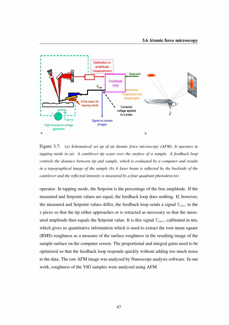
3.6 Atomic force microscopy
Figure 3.7: (a) Schematical set up of an Atomic force microscopy (AFM). It operates in
tapping mode in air. A cantilever tip scans over the surface of a sample. A feedback loop
controls the distance between tip and sample, which is evaluated by a computer and results
in a topographical image of the sample (b) A laser beam is reflected by the backside of the
cantilever and the reflected intensity is measured by a four quadrant photodetector.
operator. In tapping mode, the Setpoint is the percentage of the free amplitude. If the
measured and Setpoint values are equal, the feedback loop does nothing. If, however,
the measured and Setpoint values differ, the feedback loop sends a signal Vcorr to the
z piezo so that the tip either approaches or is retracted as necessary so that the meas-
ured amplitude then equals the Setpoint value. It is this signal Vcorr, calibrated in nm,
which gives us quantitative information which is used to extract the root mean square
(RMS) roughness as a measure of the surface roughness in the resulting image of the
sample surface on the computer screen. The proportional and integral gains need to be
optimized so that the feedback loop responds quickly without adding too much noise
to the data. The raw AFM image was analysed by Nanoscope analysis software. In our
work, roughness of the YIG samples were analysed using AFM.
47
3.7 Polarised neutron reflectivity
3.7 Polarised neutron reflectivity
Polarised neutron reflectivity (PNR) is a layer selective technique based on the mag-
netic interactions between the neutron magnetic moment and the magnetisation of the
medium. This gives us the magnetisation profile of the film and structural information
such as film thickness and interface roughness. It is a unique technique which gives
quantitative information about the magnetic moment of the sample in the monolayer
range. In a polarised neutron reflectivity experiment, the magnetisation of the film is
saturated along the direction of the neutron spin and we measure the reflectivity for
the two neutron spin states. The neutron reflection amplitude is sensitive to the surface
roughness, from this we can estimate the interface roughness of the film, within the
range 0-50 A [124]. Also, from the fringe spectra obtained due to the multiple inter-
ference of the neutron beam within the sample layers, we can obtain the thickness of
each layer of the film.
A neutron can be represented as a plane wave of wave vector k in three dimensions
as
ψ(k, r) = eik.r (3.10)
where r is the position vector of neutron in space.
In matter the neutron interacts through a neutron potential and a magnetic potential
which affect the magnitude of k. The strength of these potentials are characterised by
scalar coherent scattering lengths. The propagation of single neutron plane wave can
be represented by a time-independent Schrodinger equation:[−~2
2m 52 +V (r)
]ψ = Eψ (3.11)
where V (r) accounts for the potential energy of the neutron, m is the neutron mass and
E represents the total energy of the neutron.
Now, in a continuous medium with density N , consisting of a single isotope of a
48
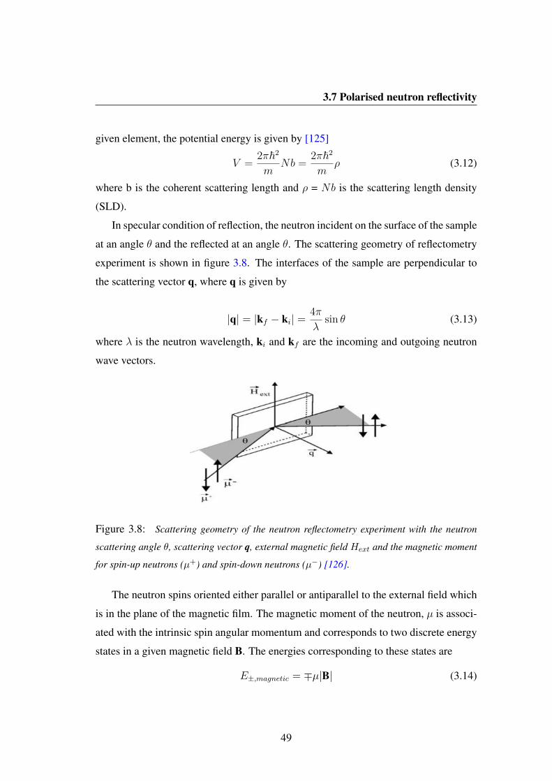
3.7 Polarised neutron reflectivity
given element, the potential energy is given by [125]
V = 2π~2
mNb = 2π~2
mρ (3.12)
where b is the coherent scattering length and ρ = Nb is the scattering length density
(SLD).
In specular condition of reflection, the neutron incident on the surface of the sample
at an angle θ and the reflected at an angle θ. The scattering geometry of reflectometry
experiment is shown in figure 3.8. The interfaces of the sample are perpendicular to
the scattering vector q, where q is given by
|q| = |kf − ki| =4πλ
sin θ (3.13)
where λ is the neutron wavelength, ki and kf are the incoming and outgoing neutron
wave vectors.
Figure 3.8: Scattering geometry of the neutron reflectometry experiment with the neutron
scattering angle θ, scattering vector q, external magnetic field Hext and the magnetic moment
for spin-up neutrons (µ+) and spin-down neutrons (µ−) [126].
The neutron spins oriented either parallel or antiparallel to the external field which
is in the plane of the magnetic film. The magnetic moment of the neutron, µ is associ-
ated with the intrinsic spin angular momentum and corresponds to two discrete energy
states in a given magnetic field B. The energies corresponding to these states are
E±,magnetic = ∓µ|B| (3.14)
49
3.7 Polarised neutron reflectivity
where the plus (minus) sign denotes the direction of spin parallel (anti-parallel) to
the magnetic induction. For a grazing incidence the interaction with the film can be
described with an effective potential given by the sum of a nuclear and a magnetic
component, Zeeman interaction. This potential is given by
V = 2π~2
mNbnuc − ~µ.B = 2π~2
m(ρn ± ρm) (3.15)
where N and bnuc denote the atomic density and coherent nuclear scattering length.
The quantity, ρn = Nbnuc is the nuclear scattering length density whereas the magnetic
contribution to the potential is expressed in terms of magnetic SLD, ρm = Nbmag. The
first term represents the interaction of the neutron with the nucleus and the second term
signifies the interaction of neutron with the magnetic field. So, the potential V + and
V − for spin up and spin down neutrons can be expressed as follows [126]:
V ± = 2π~2
m(Nbnuc ±Nbmag) (3.16)
As the nuclear and magnetic SLD are of same order of magnitude, PNR is very sens-
itive to magnetic structures. The reflectivity of the sample can be derived by solving
the Schrodinger equation (3.11) using the potential mentioned above. The spin-up and
spin-down reflectivities R+ and R− can be expressed as
R± =q −
√q2 − 16π(ρn ± ρm)
q +√q2 − 16π(ρn ± ρm)
(3.17)
The reflectivity R = 1 upto a critical edge qc =√
16π(ρn ± ρm), which is of the order of
0.01 A−1 for most of the materials. Beyond this point, the reflectivity decays rapidly
with a mean asymptotic q−4z dependence [127].
For polarised neutron reflectivity, we define spin asymmetry SA as
SA = (R+ −R−)(R+ +R−) (3.18)
where R+ and R− are the spin up and spin down reflectivities. SA gives a measure of
the difference in the reflectivity due to the spin dependent magnetic interaction.
50
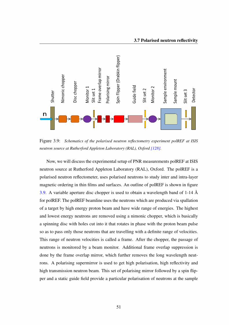
3.7 Polarised neutron reflectivity
Figure 3.9: Schematics of the polarised neutron reflectometry experiment polREF at ISIS
neutron source at Rutherford Appleton Laboratory (RAL), Oxford [128].
Now, we will discuss the experimental setup of PNR measurements polREF at ISIS
neutron source at Rutherford Appleton Laboratory (RAL), Oxford. The polREF is a
polarised neutron reflectometer, uses polarised neutrons to study inter and intra-layer
magnetic ordering in thin films and surfaces. An outline of polREF is shown in figure
3.9. A variable aperture disc chopper is used to obtain a wavelength band of 1-14 A
for polREF. The polREF beamline uses the neutrons which are produced via spallation
of a target by high energy proton beam and have wide range of energies. The highest
and lowest energy neutrons are removed using a nimonic chopper, which is basically
a spinning disc with holes cut into it that rotates in phase with the proton beam pulse
so as to pass only those neutrons that are travelling with a definite range of velocities.
This range of neutron velocities is called a frame. After the chopper, the passage of
neutrons is monitored by a beam monitor. Additional frame overlap suppression is
done by the frame overlap mirror, which further removes the long wavelength neut-
rons. A polarising supermirror is used to get high polarisation, high reflectivity and
high transmission neutron beam. This set of polarising mirror followed by a spin flip-
per and a static guide field provide a particular polarisation of neutrons at the sample
51

3.8 Ferromagnetic resonance technique
position. The flipping elements are characterised by high flipping efficiency over the
entire wavelength range and the beam size. The detected neutron beam is then norm-
alised by a second monitor placed before the sample. The beam is collimated by a slit
and directed towards the sample, that sits between the coils of an electromagnet. The
sample is mounted in a high precision sample stage. The reflected neutrons are passed
through a second set of slits and finally detected by a 3He single detector. Require-
ments for magnetic field are achieved through bipolar electromagnet (for small fields
upto 1.5 T) and superconducting magnet (for high fields upto 10 T). Temperature down
to 2 K is achieved with the use of continuous flow cryostat. The average size of the
sample used is roughly 20 x 20 mm2 to get a decent count rate within reasonable q
range.
3.8 Ferromagnetic resonance technique
The magnetization dynamics of YIG thin films are investigated by the microwave tech-
nique, called ferromagnetic resonance (FMR). The FMR technique has been widely
used for the high frequency characterisation of magnetic thin films. We can use the
FMR to study the magneto static properties, for example, anisotropies [129, 130], ex-
change coupling [131–133], and also the spin dynamics; damping constant [134, 135],
g factor [135, 136], etc. The precession frequency of a ferromagnet lies at the mi-
crowave region, ranged from 0.1 to 100 GHz. Main principle of the FMR technique
is to apply a torque on the magnetic moment by applying a rf transverse magnetic
field pulse hrf which results in the precessional motion of magnetisation M about the
direction of an external magnetic field. The magnetisation follows a helical trajectory
due to energy dissipation and this behaviour can be described by the LLG equation
2.7, in section 2.3.1 . In VNA-FMR technique, using a Vector network analyser an
electromagnetic wave can be sent to the sample. The incident wave will be reflec-
ted and/or transmitted after interacting with the sample (Fig.3.10a). By analysing the
reflectance/transmittance,which is the ratio of reflected, transmitted power to that of
52
3.8 Ferromagnetic resonance technique
incident, we can find the scattering parameters (S11, S22, S12, S21), from which we
can extract the properties of the sample. Figure 3.10b shows a two-port device under
Figure 3.10: (a) The incident wave will be reflected and/or transmitted after entering the
device under test (DUT) (b) Two-port device S-parameters model [137].
test (DUT) along with the corresponding four S-parameters. For a two port device the
S-parameters equations can be written as
b1 = S11a1 + S12a2 (3.19)
b2 = S21a1 + S22a2 (3.20)
where S11 and S22 are the reflection coefficients at the port 1 and port 2 respectively,
whereas S12 and S21 represent the transmission coefficients. So, a microwave leaving
the device under test (DUT) (b1 or b2) is a linear combination of the waves incident on
the DUT (a1 or a2). Terminating the DUT with the characteristic impedance Z0 = 50 Ωallows the extraction of the individual S-parameters. At port 2, if a 50 Ω termination is
present, a2 becomes zero, resulting in S11 and S21. We can apply the same principle in
the reverse direction to get S22 and S12 by setting a1 to zero, as shown in equation 3.21
and 3.22.
S11 = b1
a1
∣∣∣∣∣a2=0
S12 = b1
a2
∣∣∣∣∣a1=0
(3.21)
S21 = b2
a1
∣∣∣∣∣a2=0
S22 = b2
a2
∣∣∣∣∣a1=0
(3.22)
For the FMR measurements, we can sweep the microwave excitation frequency at
a fixed bias field or at fixed excitation frequency the static external field can be swept
53

3.8 Ferromagnetic resonance technique
to achieve the resonance condition. The experimental setup is shown in figure 3.11,
where vector network analyser serves as the source and detector of the signal which is
guided by the probes. It compares the incoming to the outgoing signals with respect to
their amplitude and phase so as to measure the absorption of the sample as a function
of frequency. The magnetic sample is mounted on the top of the signal lines of a
coplanar waveguide (CPW) and the microwave is conducted into coplanar waveguide.
The sample is swept through the resonance condition by means of an external field.
The measured FMR signal is proportional to the field derivative of the imaginary part
of the ac susceptibility.
Figure 3.11: Schematic of FMR technique using Vector network analyser. A 50 Ω impedance
matched waveguide is placed at the centre of DC magnetic field Hext and a microwave field
hrf is applied transverse to the DC field. The sample is placed with film-side down on top of
the waveguide.
We can also use a lock-in amplifier detection technique for our FMR measure-
ments. Figure 3.12 shows the block diagram of experimental set up of FMR using
lock-in amplifier. Here the thin sample is mounted with film-side down onto the top
of the CPW, placed in the centre of the electromagnet that provides the dc bias field.
The electromagnet has a gap of about 5 cm and a maximum field of 300 mT at 10 A
54

3.8 Ferromagnetic resonance technique
current can be applied, controlled by KEPCO power supply. The rf microwave source
is a broadband microwave generator with maximum power 25 dBm. Large power ex-
citation will drive the magnetization precession in non-linear region. Also the signal
will be reduced and broadened. So, in order to determine the lineshapes and width pre-
cisely, it is better to use low power to avoid the non-linear region. The signal intensity
is proportional to the squre root of power, Vs ∝√P [138]. In our measurements, the
microwave frequency is kept constant and the static external magnetic field is swept to
obtain the resonance field. The coplanar waveguide system operates in pulse modula-
tion mode. For this, reference pulse signal port of the microwave generator is connec-
ted to the low frequency output port of the lock in amplifier so as to keep the reference
signal frequency at 73 Hz. At this frequency, we obtained a good signal to noise ratio.
The signal generator sends the microwave current to the sample mounted on a wave-
guide and the transmitted rf FMR signals from the magnetic sample are detected by
means of a schottky diode, the output of which is sent to the lock in amplifier. The
schottky diode acts as a microwave transducer, i.e. a microwave power is transduced
into the voltage. The lock in amplifier then multiplies the diode voltage with the ref-
erence signal pulse modulated at 73 Hz and integrates the result over a certain time to
give the output voltage. This lock-in technique is useful to enhance the signal to noise
ratio.
55
3.8 Ferromagnetic resonance technique
Figure 3.12: Schematic of lock-in amplifier detection technique for FMR measurements.
The sample is mounted on the CPW which is placed at the centre of the electromagnet. The
microwave generator sends the microwave current to the magnetic sample and the transmitted
signals from the sample are detected using a schottky diode and the output is finally sent to the
lock-in amplifier.
56

CHAPTER 4
Structural and morphological properties
of nm-thick YIG films
57

4.1 Introduction
4.1 Introduction
Yttrium Iron Garnet (YIG) films were a subject of intensive research since the past
ten years. Previously in 1970s, bulk YIG crystals and micrometer thick films grown
by liquid phase epitaxy (LPE) have been widely used for the implementation of mi-
crowave devices [139]. In recent years, YIG proved to be an excellent material in
the emerging field of magnonics [21, 140–142] and spin caloritronics [[37, 38, 143].
However, integration of YIG based spintronic devices requires thin films with high
structural quality to ensure good magnetic and dynamic properties, and in particular to
develop efficient YIG-based magnetic heterostructures for information transfer. All of
the growth techniques for YIG involve the use of high temperatures (>700 C) either
during the growth, in-situ annealing or in post-growth annealing which can cause sig-
nificant changes in the structural characteristics. To our knowledge, up to now no de-
tailed studies have been carried out on the effect of high temperature annealing on the
YIG/GGG interface despite the fact that YIG-GGG combination has been used widely
in the spintronics community [38, 144–147]. In this chapter, we are interested in the
structural properties of YIG where small changes at the interface can have significant
effects on the fundamental properties of YIG. Our nm-thick single crystal YIG films
were deposited on (111) oriented 0.5 mm thick GGG substrates by RF magnetron sput-
tering followed by high temperature annealing at 850C in air. Annealed YIG samples
are transparent with a pale yellow colour. The as-deposited films on the substrates are
amorphous and non magnetic. The crystallinity of the film and the smooth surface are
achieved after their annealing.
The structural quality, lattice parameter, thickness, and surface roughness of the
YIG films were analyzed using x-ray diffraction (XRD), x-ray reflectivity (XRR) and
atomic force microscopy (AFM). For this study, a series of thin YIG films with differ-
ent thicknesses ranging from 8 nm to 250 nm were deposited under the same deposition
condition on the GGG substrate. The film-substrate interface is strongly influenced by
the annealing conditions which can affect the structural and compositional behaviour
of the films. To understand the influence of annealing at the film-substrate interface we
58
4.2 Structural properties
carried out an atomic-scale investigation of the YIG/GGG interface using aberration-
corrected scanning transmission electron microscopy (STEM).
4.2 Structural properties
4.2.1 X-ray reflectivity
In this section, the structural properties of thin YIG films were studied by x-ray re-
flectivity. This allows us to find the thickness of the film, growth rate of the material,
surface and interface roughness and the density.
Figure 4.1: X-ray reflectivity (Cu Kα, λ = 1.54 A radiation) of a typical YIG film before
annealing (a) and after annealing (b). The points are the measured data and the line is a best
fit whose parameters are cited in the Table 4.1. A very good fit is obtained for the unnealed
sample with a single layer of YIG. However, for the annealed sample a good fit could only be
obtained by incorporating an interface region instead of a sharp GGG/YIG interface.
Figure 4.1 (a) shows the low angle x-ray reflectivity (Cu Kα, λ = 1.54 A radiation)
of an unnealed 42 nm YIG film, whose thickness was determined from the angular
positions of the Kiessig fringes (inset of figure 4.1a) by using equation 3.4 (section
3.4.1). The reflectivity is measured at grazing incidence including the straight-through
beam such that the region below ∼ 0.4 is due to the beam footprint. This is followed
59
4.2 Structural properties
by a sharp decrease in the intensity at the critical angle. We measured the thickness of
the films before (42 nm) and after annealing (40 nm). After annealing the thickness
of the films decreases by a very small amount. The slow exponential decay of the
reflectivity curve indicates a smooth surface of the annealed film.
The reflectivity curves are fitted using the software Bede to get further information
about the chemical nature of the YIG/GGG interface and also the density. An example
of the X-ray reflectivity (XRR) curve with its fitting is shown in figure 4.1 (a) and (b)
for a typical YIG sample before (42 nm) and after annealing (40 nm), respectively. The
points are the measured data and the red solid line is a best fit to the reflectivity curve.
The parameters obtained from the fitting in each case are cited in the table 4.1. For the
unnealed sample, the densities of the YIG and substrate are about 96 % of the bulk.
For the annealed sample, the total thickness of the film is reduced but the interesting
point is that in order to obtain the best fit for the x-ray data, we have to include an
additional layer at the interface (figure 5.14). This gives us an indication that there
may be diffusion at the interface. Although, we obtained a good fit using only a YIG
layer with the goodness of fit (GOF = 0.05), but the density obtained from the fit for
the GGG was only 91% that of bulk GGG. A much better fit is obtained by using a
trilayer system of GGG/∼ 50-60 A of Gd-rich layer/YIG where the interface layer has
a density that is reduced by about 13%.
With the help of additional structural information from the TEM results (section
4.5.1), we model this interfacial region as a mixed layer of YIG and Gd (YIG1 and
Gd in Table 4.1). This shows that we are not relying on a specific crystal structure
of the compound GdIG to explain the results. Because this diffused layer will not
be stoichiometrically perfect. So, the interface layer is modelled by allowing its total
thickness to reach that of the dead layer (6 nm) and by incorporating significant rough-
ness and grading in the layer. In this fit, the roughness is modelled as a Gaussian
with the full width at half maximum representing the standard deviation of an effect-
ive roughness. Here, the grading is representing the interdiffusion and the roughness
is produced by terraces or steps, for example. However, it is difficult to distinguish
60
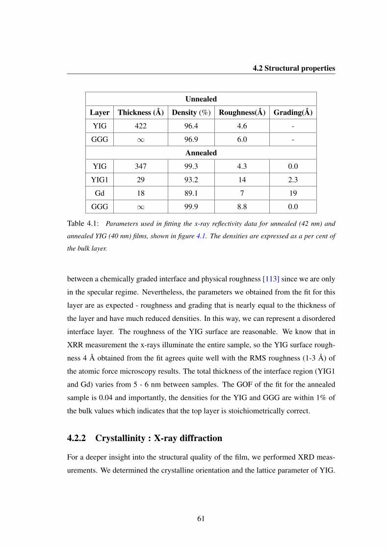
4.2 Structural properties
Unnealed
Layer Thickness (A) Density (%) Roughness(A) Grading(A)
YIG 422 96.4 4.6 -
GGG ∞ 96.9 6.0 -
Annealed
YIG 347 99.3 4.3 0.0
YIG1 29 93.2 14 2.3
Gd 18 89.1 7 19
GGG ∞ 99.9 8.8 0.0
Table 4.1: Parameters used in fitting the x-ray reflectivity data for unnealed (42 nm) and
annealed YIG (40 nm) films, shown in figure 4.1. The densities are expressed as a per cent of
the bulk layer.
between a chemically graded interface and physical roughness [113] since we are only
in the specular regime. Nevertheless, the parameters we obtained from the fit for this
layer are as expected - roughness and grading that is nearly equal to the thickness of
the layer and have much reduced densities. In this way, we can represent a disordered
interface layer. The roughness of the YIG surface are reasonable. We know that in
XRR measurement the x-rays illuminate the entire sample, so the YIG surface rough-
ness 4 A obtained from the fit agrees quite well with the RMS roughness (1-3 A) of
the atomic force microscopy results. The total thickness of the interface region (YIG1
and Gd) varies from 5 - 6 nm between samples. The GOF of the fit for the annealed
sample is 0.04 and importantly, the densities for the YIG and GGG are within 1% of
the bulk values which indicates that the top layer is stoichiometrically correct.
4.2.2 Crystallinity : X-ray diffraction
For a deeper insight into the structural quality of the film, we performed XRD meas-
urements. We determined the crystalline orientation and the lattice parameter of YIG.
61

4.2 Structural properties
We first started with the results of 2θ-ω scan of a (111) - oriented GGG substrate
with and without the monochromator, as shown in figure 4.2 (a) and (b) respectively.
Without the monochromator we can see two peaks of GGG corresponding to Cu Kα1
and Cu Kα2 radiation. With the use of monochromator, a single crystalline (444) peak
is observed at 2θ = 51.03 which corresponds to the lattice constant of 12.383 A.
Figure 4.2: (a) X-ray diffraction for a GGG substrate without the monochromator showing
two peaks of GGG. (b) XRD spectra with monochromator showing a single crystalline (444)
peak of the substrate with a lattice constant of 12.383 A.
Figure 4.3 shows the XRD scan of a YIG sample without the monochromator,
where the YIG (444) peak has two clearly resolved Kα1 and Kα2 lines. The use of
monochromator allows easier identification of peaks with Cu Kα1 wavelength only. A
monochromator was installed to filter out the Cu kα2 and to only observe the Cu kα1.
For all our XRD measurements, the monochromator was used for better investigation
of the YIG peaks. For the unnealed YIG sample, only the substrate peak is visible
because the as-deposited YIG samples are amorphous.
Figure 4.4 presents the X-ray diffraction (XRD) spectra for four samples of YIG
with thicknesses 30, 50, 78 and 250 nm. For all these samples, the YIG (444) peak
are observed at lower angle than the substrate peak. These data show the evolution of
a peak with the sample thickness. With increase in sample thickness the intensity of
62

4.2 Structural properties
Figure 4.3: X-ray diffraction for a 250 nm thick YIG film without the monochromator which
shows the YIG (444) peaks corresponding to both Cu Kα1 and Cu Kα2 radiation.
YIG (444) peak increases. This is because as the thickness increases we are adding
more atomic planes and we will have more constructive interference. The XRD peak
with the highest intensity is observed at 2θ = 50.57 for the thicker film of 250 nm.
Figure 4.5 shows the XRD rocking curve of 250 nm YIG film which exhibit a FWHM
of 0.0072 ± 0.0001 degrees confirming the high crystalline quality. For thinner films
below 30 nm, it was difficult to distinguish between the YIG peak and substrate peak.
The lattice constant is calculated from the Gaussian fit of the YIG peak for each sample.
The lattice constant as a function of thickness is plotted in figure 4.6. Inset shows the
gaussian fit of YIG peak for 250 nm thick film, giving lattice constant of 12.491 ±0.002 A. The lattice parameter of bulk YIG is 12.376 A. This slight increase in lattice
parameter might be due to the rhombohedral distortion in the YIG crystalline lattice
[148]. This variation of the XRD spectra with respect to the film thickness tends to
give an indication towards a critical thickness for strain relaxation. The variation of
lattice constant with thickness is also reported in ref. [149] where the lattice constant
of sputtered YIG varies from 12.427 A to 12.390 A for the thickness range 16 nm to
164 nm, respectively.
63

4.2 Structural properties
Figure 4.4: The YIG has a (111) crystalline orientation and films develop a diffraction peak.
Intensity of the peak varies as a function of thickness that corresponds to a lattice constant of
12.4905 ± 0.002 A for 250 nm film compared to 12.376 A for bulk YIG. For the thinnest films,
the YIG peak is masked by the substrate peak. The peak at 51.03 corresponds to the GGG
substrate with the out of plane lattice constant of 12.383 A.
Figure 4.5: XRD rocking curve of a 250 nm YIG film exhibiting FWHM of 0.0072 ± 0.0001
degrees showing the excellent crystalline quality of our YIG films.
64
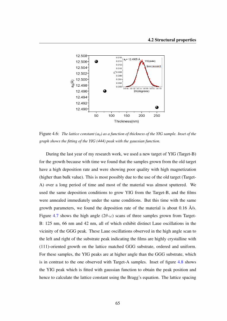
4.2 Structural properties
Figure 4.6: The lattice constant (a0) as a function of thickness of the YIG sample. Inset of the
graph shows the fitting of the YIG (444) peak with the gaussian function.
During the last year of my research work, we used a new target of YIG (Target-B)
for the growth because with time we found that the samples grown from the old target
have a high deposition rate and were showing poor quality with high magnetization
(higher than bulk value). This is most possibly due to the use of the old target (Target-
A) over a long period of time and most of the material was almost sputtered. We
used the same deposition conditions to grow YIG from the Target-B, and the films
were annealed immediately under the same conditions. But this time with the same
growth parameters, we found the deposition rate of the material is about 0.16 A/s.
Figure 4.7 shows the high angle (2θ-ω) scans of three samples grown from Target-
B: 125 nm, 66 nm and 42 nm, all of which exhibit distinct Laue oscillations in the
vicinity of the GGG peak. These Laue oscillations observed in the high angle scan to
the left and right of the substrate peak indicating the films are highly crystalline with
(111)-oriented growth on the lattice matched GGG substrate, ordered and uniform.
For these samples, the YIG peaks are at higher angle than the GGG substrate, which
is in contrast to the one observed with Target-A samples. Inset of figure 4.8 shows
the YIG peak which is fitted with gaussian function to obtain the peak position and
hence to calculate the lattice constant using the Bragg’s equation. The lattice spacing
65

4.2 Structural properties
Figure 4.7: High angle XRD scans of YIG films of thickness 125, 66 and 42 nm grown on the
GGG substrate showing single crystalline YIG (444) peak, from which the lattice spacing of the
YIG (444) planes is determined. All of the samples exhibit distinct Laue oscillations on either
side of the substrate peak indicating the films are highly crystalline, ordered and uniform.
66

4.2 Structural properties
between the adjacent YIG (444) planes is 7.132 A, 7.133 A, and 7.137 A corresponds
to YIG cubic lattice constants of 12.353 A, 12.355 A and 12.3617 A for the 125, 66
and 42 nm films, respectively. In ref. [65], the YIG peaks have also appeared on the
right side of the GGG peak. For our 42 nm thick YIG, the intenisty of YIG peak is
very low and hence it was hard to distinguish from those of the substrate. Figure 4.8
shows the variation of lattice constant as a function of thickness. With decrease in film
thickness, the lattice constant shows a slight increase. This thickness dependence of
lattice constant was also observed for off-axis sputtered YIG films with thicknesses 10,
20, 50 and 80 nm [65]. From the comparison of our XRD spectra, we found that films
grown at much slower rate from the Target-B shows Laue oscillation. Also, the lattice
constant is more close to the bulk value of YIG which indicates minimal distortion or
strain as compared to the films grown from the Target-A.
Figure 4.8: The lattice constant (a0) as a function of thickness of the YIG sample. Inset
of the graph shows the fitting of the YIG (444) peak with the gaussian function used for the
determination of the lattice constant of YIG.
Altogether, we believe that we have found a set of growth parameters that allow
the growth of high quality single crystalline YIG films on the GGG substrate from a
polycrystalline target.
67
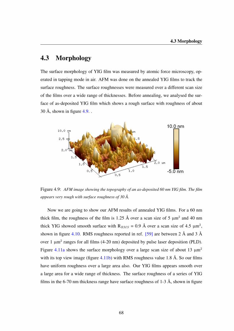
4.3 Morphology
4.3 Morphology
The surface morphology of YIG film was measured by atomic force microscopy, op-
erated in tapping mode in air. AFM was done on the annealed YIG films to track the
surface roughness. The surface roughnesses were measured over a different scan size
of the films over a wide range of thicknesses. Before annealing, we analysed the sur-
face of as-deposited YIG film which shows a rough surface with roughness of about
30 A, shown in figure 4.9. .
Figure 4.9: AFM image showing the topography of an as-deposited 60 nm YIG film. The film
appears very rough with surface roughness of 30 A.
Now we are going to show our AFM results of annealed YIG films. For a 60 nm
thick film, the roughness of the film is 1.25 A over a scan size of 5 µm2 and 40 nm
thick YIG showed smooth surface with RRMS = 0.9 A over a scan size of 4.5 µm2,
shown in figure 4.10. RMS roughness reported in ref. [59] are between 2 A and 3 A
over 1 µm2 ranges for all films (4-20 nm) deposited by pulse laser deposition (PLD).
Figure 4.11a shows the surface morphology over a large scan size of about 13 µm2
with its top view image (figure 4.11b) with RMS roughness value 1.8 A. So our films
have uniform roughness over a large area also. Our YIG films appears smooth over
a large area for a wide range of thickness. The surface roughness of a series of YIG
films in the 6-70 nm thickness range have surface roughness of 1-3 A, shown in figure
68
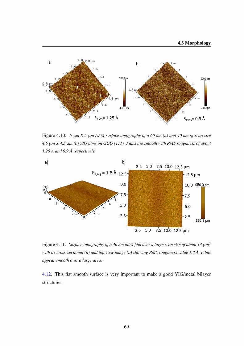
4.3 Morphology
Figure 4.10: 5 µm X 5 µm AFM surface topography of a 60 nm (a) and 40 nm of scan size
4.5 µm X 4.5 µm (b) YIG films on GGG (111). Films are smooth with RMS roughness of about
1.25 A and 0.9 A respectively.
Figure 4.11: Surface topography of a 40 nm thick film over a large scan size of about 13 µm2
with its cross-sectional (a) and top view image (b) showing RMS roughness value 1.8 A. Films
appear smooth over a large area.
4.12. This flat smooth surface is very important to make a good YIG/metal bilayer
structures.
69
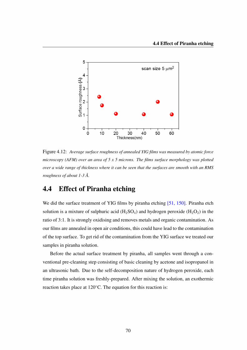
4.4 Effect of Piranha etching
Figure 4.12: Average surface roughness of annealed YIG films was measured by atomic force
microscopy (AFM) over an area of 5 x 5 microns. The films surface morphology was plotted
over a wide range of thickness where it can be seen that the surfaces are smooth with an RMS
roughness of about 1-3 A.
4.4 Effect of Piranha etching
We did the surface treatment of YIG films by piranha etching [51, 150]. Piranha etch
solution is a mixture of sulphuric acid (H2SO4) and hydrogen peroxide (H2O2) in the
ratio of 3:1. It is strongly oxidising and removes metals and organic contamination. As
our films are annealed in open air conditions, this could have lead to the contamination
of the top surface. To get rid of the contamination from the YIG surface we treated our
samples in piranha solution.
Before the actual surface treatment by piranha, all samples went through a con-
ventional pre-cleaning step consisting of basic cleaning by acetone and isopropanol in
an ultrasonic bath. Due to the self-decomposition nature of hydrogen peroxide, each
time piranha solution was freshly-prepared. After mixing the solution, an exothermic
reaction takes place at 120C. The equation for this reaction is:
70
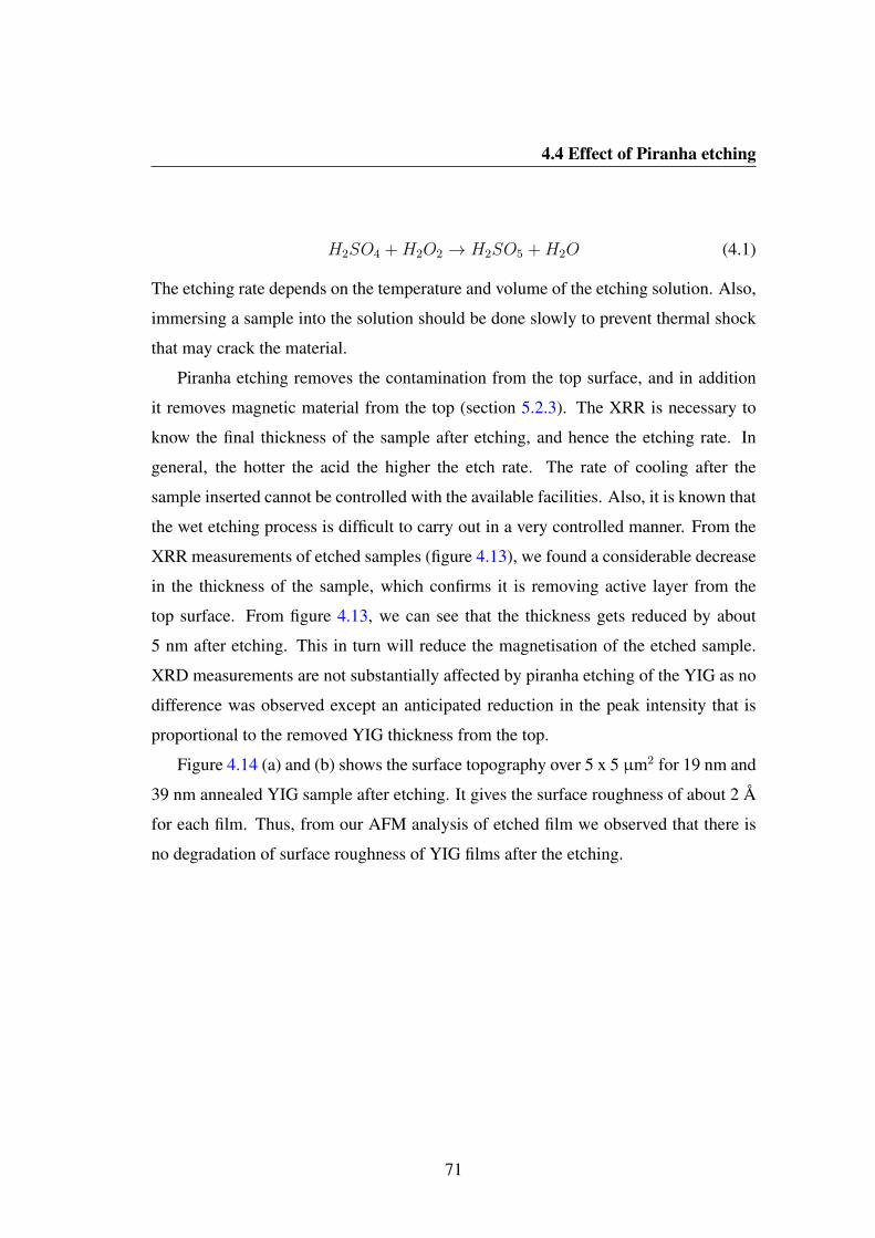
4.4 Effect of Piranha etching
H2SO4 +H2O2 → H2SO5 +H2O (4.1)
The etching rate depends on the temperature and volume of the etching solution. Also,
immersing a sample into the solution should be done slowly to prevent thermal shock
that may crack the material.
Piranha etching removes the contamination from the top surface, and in addition
it removes magnetic material from the top (section 5.2.3). The XRR is necessary to
know the final thickness of the sample after etching, and hence the etching rate. In
general, the hotter the acid the higher the etch rate. The rate of cooling after the
sample inserted cannot be controlled with the available facilities. Also, it is known that
the wet etching process is difficult to carry out in a very controlled manner. From the
XRR measurements of etched samples (figure 4.13), we found a considerable decrease
in the thickness of the sample, which confirms it is removing active layer from the
top surface. From figure 4.13, we can see that the thickness gets reduced by about
5 nm after etching. This in turn will reduce the magnetisation of the etched sample.
XRD measurements are not substantially affected by piranha etching of the YIG as no
difference was observed except an anticipated reduction in the peak intensity that is
proportional to the removed YIG thickness from the top.
Figure 4.14 (a) and (b) shows the surface topography over 5 x 5 µm2 for 19 nm and
39 nm annealed YIG sample after etching. It gives the surface roughness of about 2 A
for each film. Thus, from our AFM analysis of etched film we observed that there is
no degradation of surface roughness of YIG films after the etching.
71
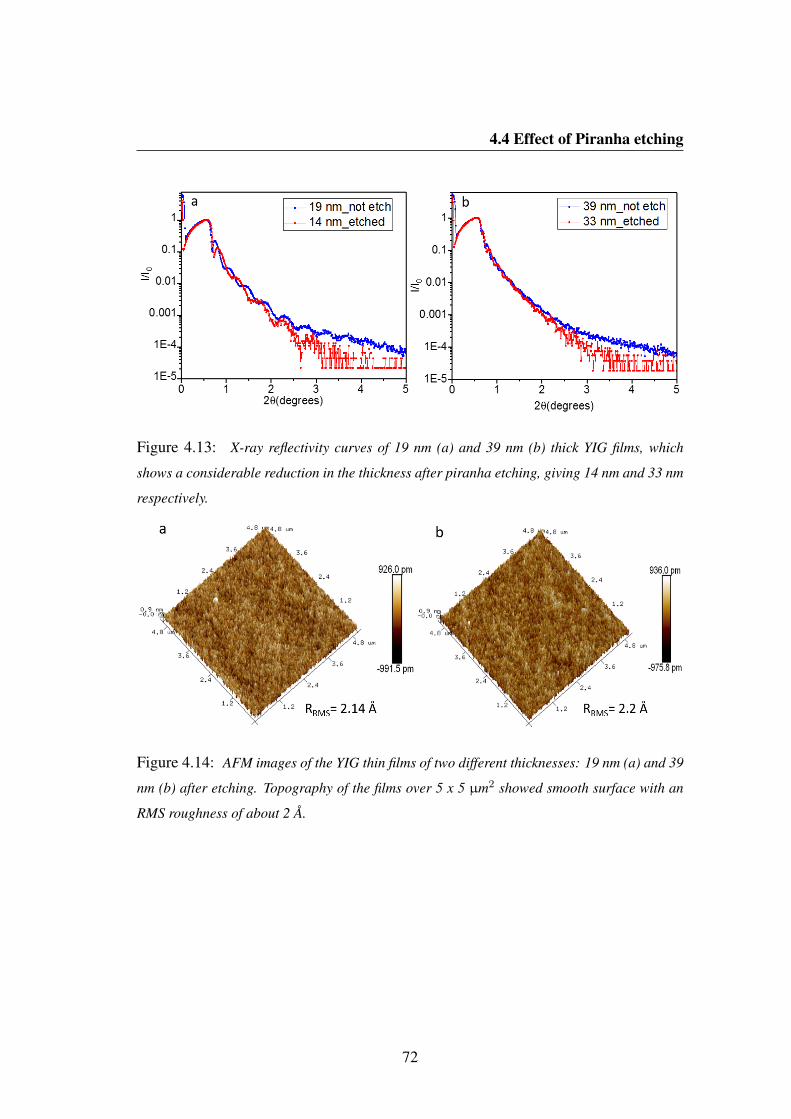
4.4 Effect of Piranha etching
Figure 4.13: X-ray reflectivity curves of 19 nm (a) and 39 nm (b) thick YIG films, which
shows a considerable reduction in the thickness after piranha etching, giving 14 nm and 33 nm
respectively.
Figure 4.14: AFM images of the YIG thin films of two different thicknesses: 19 nm (a) and 39
nm (b) after etching. Topography of the films over 5 x 5 µm2 showed smooth surface with an
RMS roughness of about 2 A.
72
4.5 Compositional analysis
4.5 Compositional analysis
4.5.1 Atomic scale investigation using scanning transmission elec-
tron microscopy (STEM)
We carried out an atomic-scale investigation of the YIG/GGG interface using aberration-
corrected scanning transmission electron microscopy (STEM) in order to get direct
confirmation of interdiffusion at the YIG/GGG interface. This work was done in col-
laboration with Q. Ramasse of SuperSTEM Laboratory in Daresbury. Scanning trans-
mission electron microscopy (STEM) and electron energy loss spectroscopy (EELS)
were carried out on a Nion UltraSTEM100 instrument operated at 100 kV acceleration
voltage. From the EELS maps, we estimated the composition profiles (and averaged
across the interface). These are known to be inaccurate for most of the edges in these
compounds. Therefore, the compositions should only be seen as indicative of trends
and the uncertainty on these numbers is of the order of 10 %.
From the High-angle annular-dark-field (HAADF) images of the interface along
the [110] zone axis, we observed a gradual transition of the intensity from the GGG
substrate to the YIG film: this is shown in figure 4.15a, with identical observations
along the entire interface. Given the sensitivity of this imaging mode to the average
atomic number, Z, of the material (the HAADF contrast is approximately proportional
to Z1.7) [151], this indicates a chemically-diffuse region at the interface, rather than
a sharp interface. This is in good agreement with our XRR fitting results. Electron
energy loss spectroscopy (EELS) provides further evidence of the interdiffusion of the
various cations across the interface. The chemical maps of Ga, Gd, O, Y and Fe were
recorded across the interface region, defined by the white rectangle in figure 4.15a.
We obtained the averaged composition profiles by integrating these maps across the
interface, which indicate a 6.5 nm wide region of mixed chemical composition. The
compositions on either side of this region correspond to the expected bulk values for
YIG and GGG, as shown in figure 4.15b.
This interdiffusion region is marked by dotted lines, for a guide to the eye in fig-
73

4.5 Compositional analysis
Figure 4.15: Analytical STEM characterisation of the YIG/GGG interface. (a) HAADF survey
image of the interface (YIG: left, GGG:right). A white box indicates the region over which
the EELS spectrum imaging was carried out, yielding compositional profiles (obtained using
tabulated Hartree-Slater cross-sections) averaged across the interface (YIG:right, GGG:left)
(c). The HAADF intensity recorded simultaneously with the EELS maps is shown in (b) with
white dotted lines indicating as a guide to the eye a ∼ 6 nm wide region over which some
interdiffusion of Gd, Y, Ga and Fe is observed (corresponding to the region marked with dotted
lines on the profiles in (c)). Panel (d) shows a higher magnification EELS analysis of the
interface (rotated 90 degrees to (a)) in the region indicated by a white box on the HAADF
survey image. Maps for Ga, Gd, O Y and Fe are presented, along with the simultaneously
acquired HAADF intensity, over which a ball model of YIG in [110] orientation is overlaid
(green balls represent Fe, blue balls represent Y, and oxygen is not represented for clarity).
Image courtesy: Q. Ramasse.
74
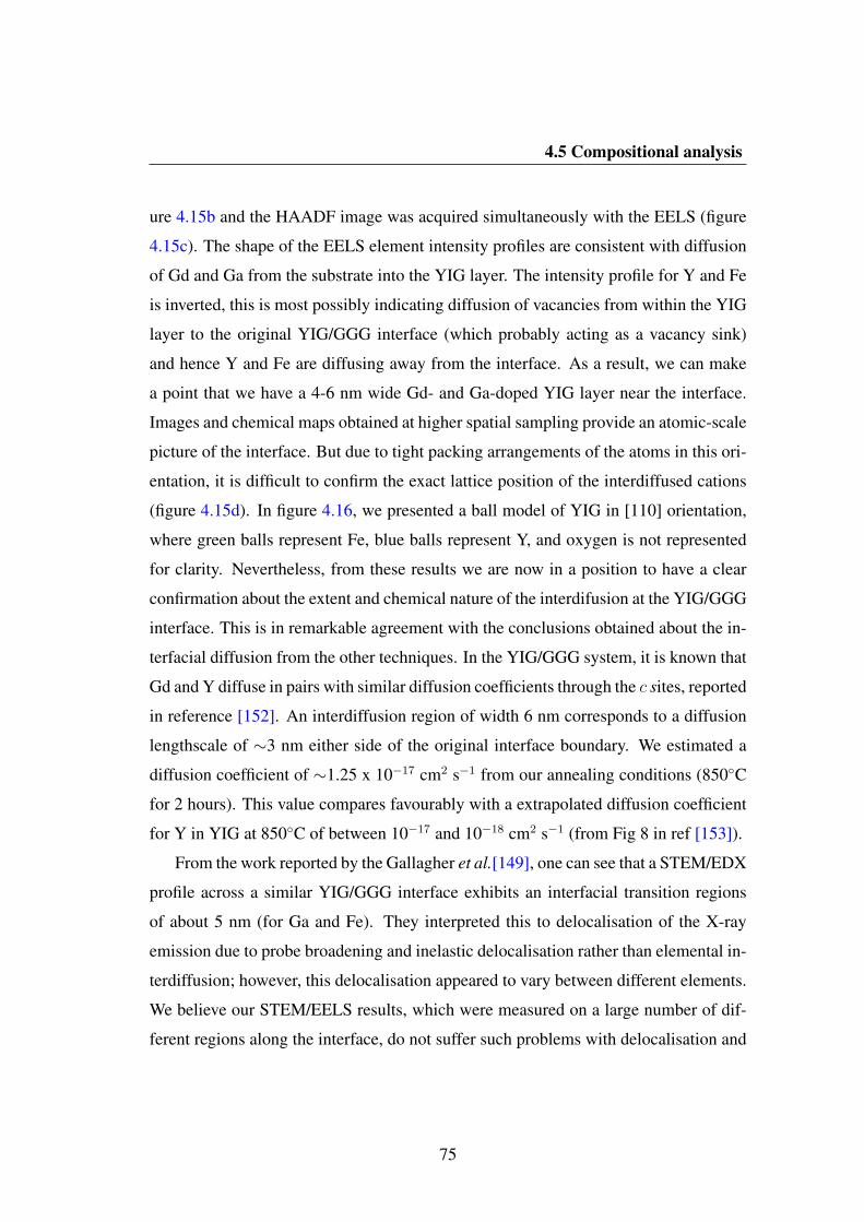
4.5 Compositional analysis
ure 4.15b and the HAADF image was acquired simultaneously with the EELS (figure
4.15c). The shape of the EELS element intensity profiles are consistent with diffusion
of Gd and Ga from the substrate into the YIG layer. The intensity profile for Y and Fe
is inverted, this is most possibly indicating diffusion of vacancies from within the YIG
layer to the original YIG/GGG interface (which probably acting as a vacancy sink)
and hence Y and Fe are diffusing away from the interface. As a result, we can make
a point that we have a 4-6 nm wide Gd- and Ga-doped YIG layer near the interface.
Images and chemical maps obtained at higher spatial sampling provide an atomic-scale
picture of the interface. But due to tight packing arrangements of the atoms in this ori-
entation, it is difficult to confirm the exact lattice position of the interdiffused cations
(figure 4.15d). In figure 4.16, we presented a ball model of YIG in [110] orientation,
where green balls represent Fe, blue balls represent Y, and oxygen is not represented
for clarity. Nevertheless, from these results we are now in a position to have a clear
confirmation about the extent and chemical nature of the interdifusion at the YIG/GGG
interface. This is in remarkable agreement with the conclusions obtained about the in-
terfacial diffusion from the other techniques. In the YIG/GGG system, it is known that
Gd and Y diffuse in pairs with similar diffusion coefficients through the c sites, reported
in reference [152]. An interdiffusion region of width 6 nm corresponds to a diffusion
lengthscale of ∼3 nm either side of the original interface boundary. We estimated a
diffusion coefficient of ∼1.25 x 10⁻¹⁷ cm2 s−1 from our annealing conditions (850C
for 2 hours). This value compares favourably with a extrapolated diffusion coefficient
for Y in YIG at 850C of between 10−17 and 10−18 cm2 s−1 (from Fig 8 in ref [153]).
From the work reported by the Gallagher et al.[149], one can see that a STEM/EDX
profile across a similar YIG/GGG interface exhibits an interfacial transition regions
of about 5 nm (for Ga and Fe). They interpreted this to delocalisation of the X-ray
emission due to probe broadening and inelastic delocalisation rather than elemental in-
terdiffusion; however, this delocalisation appeared to vary between different elements.
We believe our STEM/EELS results, which were measured on a large number of dif-
ferent regions along the interface, do not suffer such problems with delocalisation and
75
4.5 Compositional analysis
Figure 4.16: A ball model of YIG in [110] orientation is overlaid (green balls represent Fe,
blue balls represent Y, and oxygen is not represented for clarity).
hence can be attributed to chemical intermixing. This gives a good matching with our
results obtained from the XRR data fitting and room temperature magnetometry.
4.5.2 Rutherford back scattering (RBS) study
Rutherford back scattering (RBS) determines the elemental composition of a material
based on the energies of scattered alpha particles. Rutherford backscattering (RBS)
measurements were done at the CTN/IST Van de Graaff accelerator in the universal
chamber where one detector is installed at 160 scattering angle. Spectra were collec-
ted for 2 MeV 4He+. The angle of incidence was from 5 (near normal incidence) to
80 (grazing angle). This measurement is performed at Campus Tecnologico e Nuc-
lear, Instituto Superior Tecnico in Portugal. The RBS data were analysed with the IBA
DataFurnace NDF v9.6h [154] by N.P. Barradas.
For each sample, always more than one spectrum was acquired at different angles
of incidence θ. It was not possible to analyse all the spectra from one sample with the
same model (i.e. depth profile), which is an indication that the films are not homogen-
eous. A further indication of film inhomogeneity was that, the determined YIG film
76
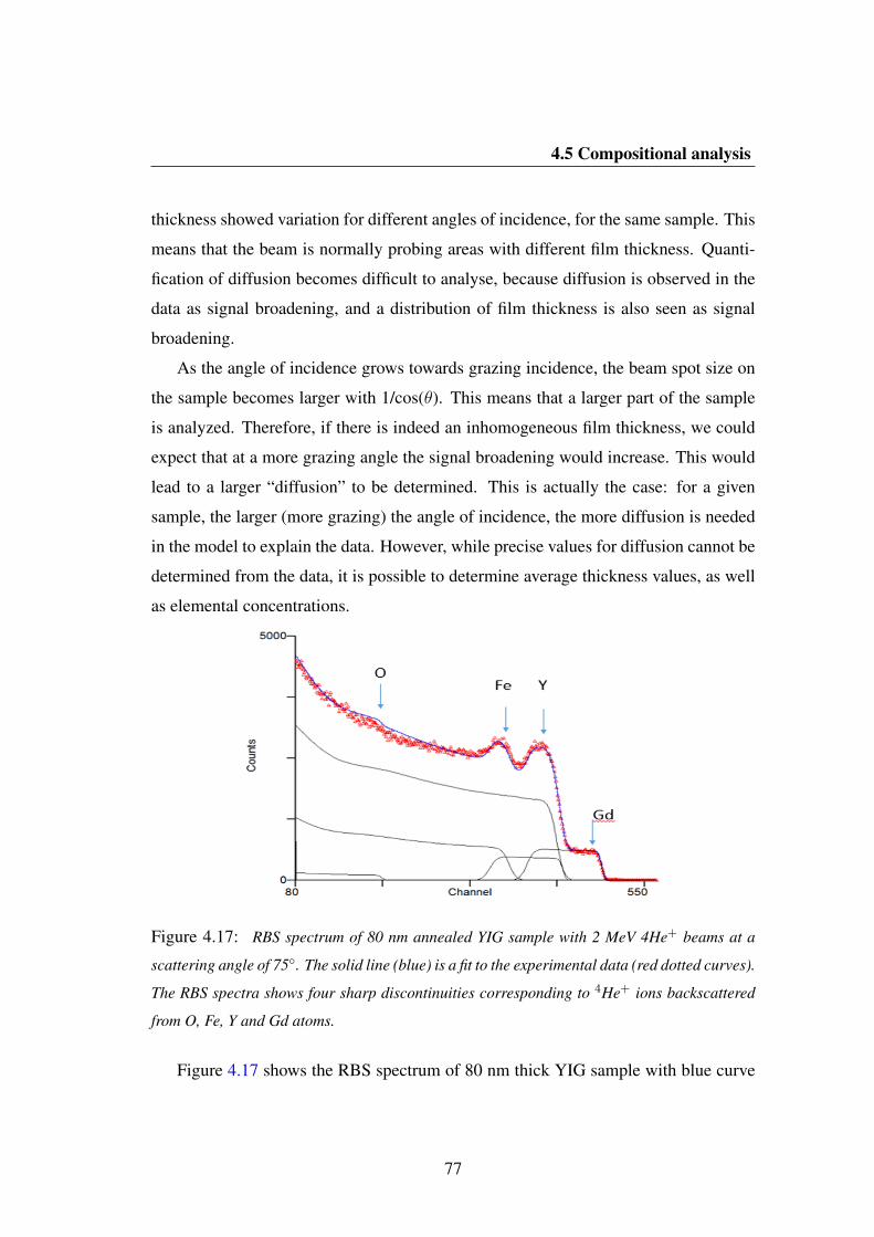
4.5 Compositional analysis
thickness showed variation for different angles of incidence, for the same sample. This
means that the beam is normally probing areas with different film thickness. Quanti-
fication of diffusion becomes difficult to analyse, because diffusion is observed in the
data as signal broadening, and a distribution of film thickness is also seen as signal
broadening.
As the angle of incidence grows towards grazing incidence, the beam spot size on
the sample becomes larger with 1/cos(θ). This means that a larger part of the sample
is analyzed. Therefore, if there is indeed an inhomogeneous film thickness, we could
expect that at a more grazing angle the signal broadening would increase. This would
lead to a larger “diffusion” to be determined. This is actually the case: for a given
sample, the larger (more grazing) the angle of incidence, the more diffusion is needed
in the model to explain the data. However, while precise values for diffusion cannot be
determined from the data, it is possible to determine average thickness values, as well
as elemental concentrations.
Figure 4.17: RBS spectrum of 80 nm annealed YIG sample with 2 MeV 4He+ beams at a
scattering angle of 75. The solid line (blue) is a fit to the experimental data (red dotted curves).
The RBS spectra shows four sharp discontinuities corresponding to 4He+ ions backscattered
from O, Fe, Y and Gd atoms.
Figure 4.17 shows the RBS spectrum of 80 nm thick YIG sample with blue curve
77
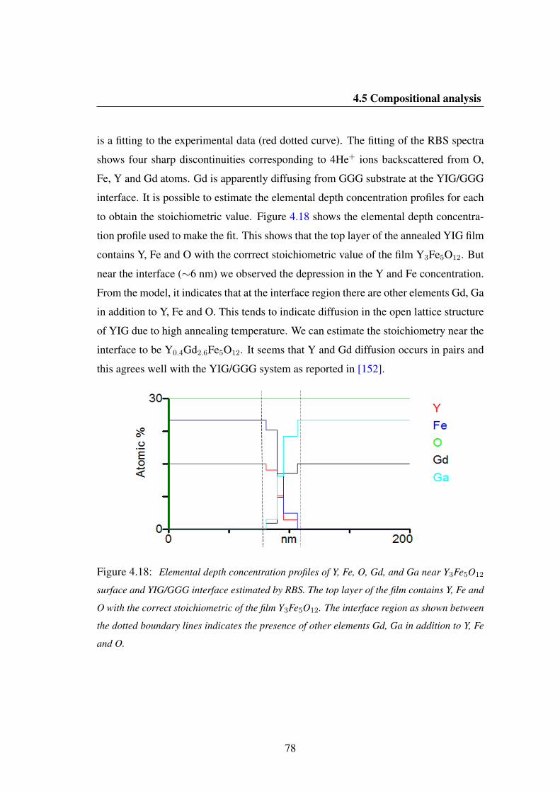
4.5 Compositional analysis
is a fitting to the experimental data (red dotted curve). The fitting of the RBS spectra
shows four sharp discontinuities corresponding to 4He+ ions backscattered from O,
Fe, Y and Gd atoms. Gd is apparently diffusing from GGG substrate at the YIG/GGG
interface. It is possible to estimate the elemental depth concentration profiles for each
to obtain the stoichiometric value. Figure 4.18 shows the elemental depth concentra-
tion profile used to make the fit. This shows that the top layer of the annealed YIG film
contains Y, Fe and O with the corrrect stoichiometric value of the film Y3Fe5O12. But
near the interface (∼6 nm) we observed the depression in the Y and Fe concentration.
From the model, it indicates that at the interface region there are other elements Gd, Ga
in addition to Y, Fe and O. This tends to indicate diffusion in the open lattice structure
of YIG due to high annealing temperature. We can estimate the stoichiometry near the
interface to be Y0.4Gd2.6Fe5O12. It seems that Y and Gd diffusion occurs in pairs and
this agrees well with the YIG/GGG system as reported in [152].
Figure 4.18: Elemental depth concentration profiles of Y, Fe, O, Gd, and Ga near Y3Fe5O12
surface and YIG/GGG interface estimated by RBS. The top layer of the film contains Y, Fe and
O with the correct stoichiometric of the film Y3Fe5O12. The interface region as shown between
the dotted boundary lines indicates the presence of other elements Gd, Ga in addition to Y, Fe
and O.
78
4.6 Conclusion
4.6 Conclusion
In this chapter, we performed a comprehensive study of the crystallinity and morpho-
logy of the RF sputtered YIG films and also the chemical nature of the YIG/GGG
interface after annealing. The influence of the deposition and annealing conditions on
the structural quality of the samples was studied by x-ray reflectivity and x-ray dif-
fraction analysis. The single crystalline (111)-oriented YIG films are grown from the
polycrystalline YIG target. From XRR results of annealed YIG sample, we identified
an interdiffusion region of about 6 nm thick at the YIG/GGG interface.
The low deposition rate and optimum target-substrate distance enabled the growth
of smooth YIG films. Our AFM results for a series of YIG films of varying thickness
confirmed that our films are smooth with roughness about 1-3 A. From x-ray reflectiv-
ity measurements we found that piranha etching removes the active layer of YIG from
the top surface while removing the contamination. The surface of the YIG films remain
smooth after etching.
The results obtained using atomic resolution STEM emphasize the impact of high
temperature annealing at the interface of YIG and GGG. This also confirms the dif-
fusion of Gd and Ga at the interface forming Gd and Ga-mixed YIG region, which
can affect the stoichiometry of YIG near the interface. Our YIG/GGG system can be
approximately represented by a two-layer model: YIG and another layer of YIG doped
with Gd. The Gd-rich YIG layer with a highly disordered structure is located near the
interface and the upper layer can be estimated as an almost perfectly formed YIG. In
addition to STEM results, RBS measurements tend to indicate that Y and Gd diffusion
in pairs. The formation of diffusion region due to high annealing temperature can lead
to structural modifications and anamolous magnetic properties of YIG as compared to
bulk YIG.
The most important result is the 4-6 nm Gd-rich diffused layer at the YIG/GGG
interface. So, there is a further scope to optimise the growth methods and annealing
conditions to minimize the diffusion. We could possibly use low temperature annealing
to avoid this interlayer mixing. We can also try to introduce a buffer layer between the
79

4.6 Conclusion
YIG and substrate interface. In summary, we suceeded to grow good quality ultrathin
YIG films by sputtering which are useful in the investigation of the origin of novel
magnetic phenomena in insulator metal hybrid structures.
80
CHAPTER 5
Magnetic properties of nm-thick YIG
films
81
5.1 Introduction
5.1 Introduction
In this chapter, we report the magnetic properties of nanometre thick RF sputtered
YIG films. For the growth of high quality thin films the lattice mismatch between
the film and the substrate is an important parameter. The lattice constant of cubic
GGG is 12.383 A which leads to negligible lattice misfit (0.03%) and makes GGG an
excellent choice as substrate. The nm-thick single crystal YIG films were deposited
on (111) oriented 0.5 mm thick GGG substrates. YIG exhibits a ferrimagnetic order
with the transition temperature of 560 K. Below the Curie temperature, the Fe3+ spins
of the a sites align antiparallel to those present at the d sites due to the superexchange
interaction and along the magnetic easy axes (111) directions (section 2.2).
Fabrication of spintronic and magnonic devices requires thin films of YIG with
high magnetic quality, even though a detail characterisation of the magnetization is
lacking. Here, we investigated the magnetic properties of single crystal YIG films by
using VSM and SQUID-VSM. The thickness dependence measurement is performed
to find the saturation magnetisation, coercivity and the thickness of the dead-layer re-
gion. Results from SQUID-VSM magnetometry have made a major contribution to
this work by measuring the magnetic moment of the samples with very high sensit-
ivity in the wide temperature range 1.8 K to 300 K. The temperature dependence of
the magnetisation M(T) shows an unexpected downturn in magnetisation in the low
temperature region which has not been reported before. These M(T) measurements
were done for different thicknesses of YIG ranging from 10 nm to 250 nm. The Curie
temperature (TC) of bulk YIG is 560 K, so we measured at high temperature to find
the value of TC for nm-thick YIG films. We carried out the surface treatment of YIG
by piranha etching to study its effect on the magnetisation of YIG. We also measured
the temperature dependence of magnetisation of YIG deposited on YAG (Y3Al5O12)
substrates and compared the M(T) results with that obtained from the YIG on GGG
substrate.
Polarised neutron reflectivity (PNR) is an excellent tool to provide magnetic in-
formation of the sample. To our knowledge so far we are the first to perform the PNR
82
5.2 Magnetometry
experiments in YIG samples to extract the magnetic information, particularly at the
YIG/GGG interface. Then, we compared our magnetometry and PNR results to get
an idea about the orientation of the magnetic moment of Gd-diffused region at the
YIG/GGG interface. Finally, we used a simple two-layer model (YIG and Gd-diffused
YIG layer) for our film to fit the M(T) curves for each YIG thickness. The correlation
between the results obtained from the magnetometry, polarised neutron reflectivity and
our fitting is very high.
5.2 Magnetometry
5.2.1 Thickness dependent magnetic properties
We have studied the thickness dependent magnetic properties of YIG on (111) GGG
substrate by using Vibrating sample magnetometer (VSM). In the following, we com-
pared our results with the values obtained for bulk YIG. At first, we measured the hys-
teresis loops as a function of applied field at 295 K to find the net magnetic moment
m and the coercivity Hc. For this, a magnetic field of 5 mT was applied in plane along
the easy axis of the sample. We set the direction of easy axis of our samples during
the growth with the help of an array of magnets attached to the shutter wheel. During
the deposition, the substrate sits at the centre of these magnets. Measurements were
carried out at constant temperature for each sample. Figure 5.1 shows a typical depend-
ence of the magnetic moment versus in plane magnetic field (m-H) of a 40 nm thick
YIG film at 295 K (blue curve). We observed that in magnetometry measurements the
signal from the thin film of YIG is dominated by the paramagnetism induced by the
Gd3+ ions in the GGG substrate generating a large background signal (black curve).
To substantiate the paramagnetism in GGG, we measured a m(T) curve at 10 mT on
cooling the GGG substrate from 300 K to 3 K as shown in figure 5.2. The temperature
dependence of the magnetization curve in GGG obeys the Curie law (∝ 1/T). The
paramagnetic background signal increases with decreasing temperature. Inset shows
83
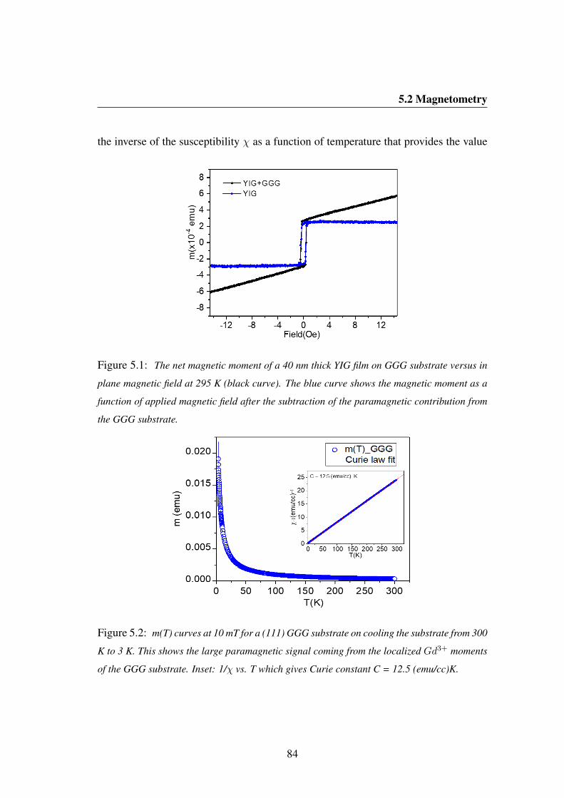
5.2 Magnetometry
the inverse of the susceptibility χ as a function of temperature that provides the value
Figure 5.1: The net magnetic moment of a 40 nm thick YIG film on GGG substrate versus in
plane magnetic field at 295 K (black curve). The blue curve shows the magnetic moment as a
function of applied magnetic field after the subtraction of the paramagnetic contribution from
the GGG substrate.
Figure 5.2: m(T) curves at 10 mT for a (111) GGG substrate on cooling the substrate from 300
K to 3 K. This shows the large paramagnetic signal coming from the localized Gd3+ moments
of the GGG substrate. Inset: 1/χ vs. T which gives Curie constant C = 12.5 (emu/cc)K.
84
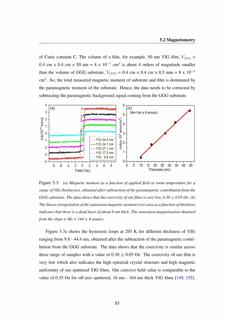
5.2 Magnetometry
of Curie constant C. The volume of a film, for example, 50 nm YIG film, Vfilm =
0.4 cm x 0.4 cm x 50 nm = 8 x 10⁻⁷ cm3 is about 4 orders of magnitude smaller
than the volume of GGG substrate, VGGG = 0.4 cm x 0.4 cm x 0.5 mm = 8 x 10⁻³
cm3. So, the total measured magnetic moment of substrate and film is dominated by
the paramagnetic moment of the substrate. Hence, the data needs to be corrected by
subtracting the paramagnetic background signal coming from the GGG substrate.
Figure 5.3: (a) Magnetic moment as a function of applied field at room temperature for a
range of YIG thicknesses, obtained after subtraction of the paramagnetic contribution from the
GGG substrate. The data shows that the coercivity of our films is very low, 0.30± 0.05 Oe. (b)
The linear extrapolation of the saturation magnetic moment over area as a function of thickness
indicates that there is a dead layer of about 6 nm thick. The saturation magnetisation obtained
from the slope is Ms = 144 ± 6 emu/cc.
Figure 5.3a shows the hysteresis loops at 295 K for different thickness of YIG
ranging from 9.8 - 44.4 nm, obtained after the subtraction of the paramagnetic contri-
bution from the GGG substrate. The data shows that the coercivity is similar across
these range of samples with a value of 0.30 ± 0.05 Oe. The coercivity of our film is
very low which also indicates the high epitaxial crystal structure and high magnetic
uniformity of our sputtered YIG films. Our coercive field value is comparable to the
value of 0.35 Oe for off-axis sputtered, 16 nm - 164 nm thick YIG films [149, 155].
85

5.2 Magnetometry
Our Hc value is about 10 times smaller than reported in ref. [156] for PLD-grown YIG
film (2 Oe) and about 100 times smaller than reported in ref.[157], which is 15-30 Oe
for different YIG thicknesses. The saturation magnetic moment m, depends linearly
on the thickness of the film (figure 5.3b). The magnetization can be obtained from the
measured magnetic moment by determining the thickness of each sample and using
the volume of the material. The linear extrapolation of the magnetic moment over area
versus thickness indicates the presence of a magnetically-inactive layer, sometimes
called a dead layer, of ∼ 6 nm. In magnetic thin films, it is common that the dead lay-
ers are usually found at the sample/substrate interface and in this YIG/GGG system,
the dead layer thickness corresponds remarkably well to the diffusion region indicated
by the x-ray reflectivity (section 4.2.1) and the STEM analysis (section 4.5.1). The
interpretation thus far is that Gd and Y have interdiffused at the interface region during
annealing, but at room temperature this interface is paramagnetic because 295 K is
well above the ordering temperature of Gd3+(which is between 65 K - 85 K) in Gd-
doped YIG [158]. The slope of this curve indicates a saturation magnetisation value
of 144 ± 6 emu/cc, which agrees well with the bulk magnetisation value Ms = 140
emu/cc at 295 K [159]. This also indicates that at room temperature the magnetization
is independent of thickness.
The Curie temperature of a ferrimagnet is given by
TC = µ√CACB (5.1)
where CA and CB are the Curie constants of Fe3+ ions on the a and d sites respectively,
and µ is the mean field constant [160].
Figure 5.4 shows the Curie temperature of a 72 nm thick YIG film. The experi-
mental data is fitted using Bloch’s T3/2 law, which describes the temperature depend-
ence of magnetisation of magnetic materials [160]. The magnetisation as a function of
temperature is given by
M(T ) = M0[1− (T/TC)3/2]β (5.2)
where M0 is the spontaneous magnetisation at absolute zero, TC is the Curie temper-
86

5.2 Magnetometry
Figure 5.4: Susceptibility versus temperature for 72 nm thick YIG film. The solid line is a fit
using the Bloch T3/2 law and this gives the value of Curie temprature 559± 4 K which is close
to the bulk value 560 K. Here β = 0.47.
ature and β is a critical exponent. This equation is an empirically modified version
of Bloch’s law to take into account the anisotropy and behaviour close to TC . The
fitting to the Bloch law illustrating that the value of TC = 559 ± 4 K, is close to the
bulk value of YIG which is 560 K [160]. This value is comparable to 551 K as re-
ported by K. P. Belov et al [161]. The observed Curie temperature in YIG is due to
the superexchange interaction between ferric ions in a and d sites mediated by the O2−
ions. Superexchange interaction is defined as an indirect exchange interaction between
two non-neighbouring magnetic ions mediated by a non-magnetic ion which is located
between the magnetic ions.
5.2.2 Temperature dependence of magnetisation
Magnetic characterisation was performed in the temperature range of 1.8 K to 350 K
in a vibrating sample superconducting quantum interference device (SQUID) magne-
tometer: MPMS3 by Quantum Design. The magnetic field was applied in plane to our
87
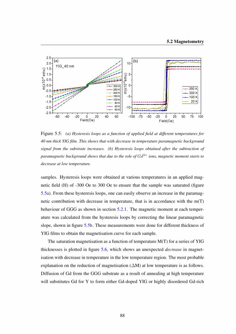
5.2 Magnetometry
Figure 5.5: (a) Hysteresis loops as a function of applied field at different temperatures for
40 nm thick YIG film. This shows that with decrease in temperature paramagnetic background
signal from the substrate increases. (b) Hysteresis loops obtained after the subtraction of
paramagnetic background shows that due to the role of Gd3+ ions, magnetic moment starts to
decrease at low temperature.
samples. Hysteresis loops were obtained at various temperatures in an applied mag-
netic field (H) of -300 Oe to 300 Oe to ensure that the sample was saturated (figure
5.5a). From these hysteresis loops, one can easily observe an increase in the paramag-
netic contribution with decrease in temperature, that is in accordance with the m(T)
behaviour of GGG as shown in section 5.2.1. The magnetic moment at each temper-
ature was calculated from the hysteresis loops by correcting the linear paramagnetic
slope, shown in figure 5.5b. These measurements were done for different thickness of
YIG films to obtain the magnetisation curve for each sample.
The saturation magnetisation as a function of temperature M(T) for a series of YIG
thicknesses is plotted in figure 5.6, which shows an unexpected decrease in magnet-
isation with decrease in temperature in the low temperature region. The most probable
explanation on the reduction of magnetisation (∆M) at low temperature is as follows.
Diffusion of Gd from the GGG substrate as a result of annealing at high temperature
will substitutes Gd for Y to form either Gd-doped YIG or highly disordered Gd-rich
88
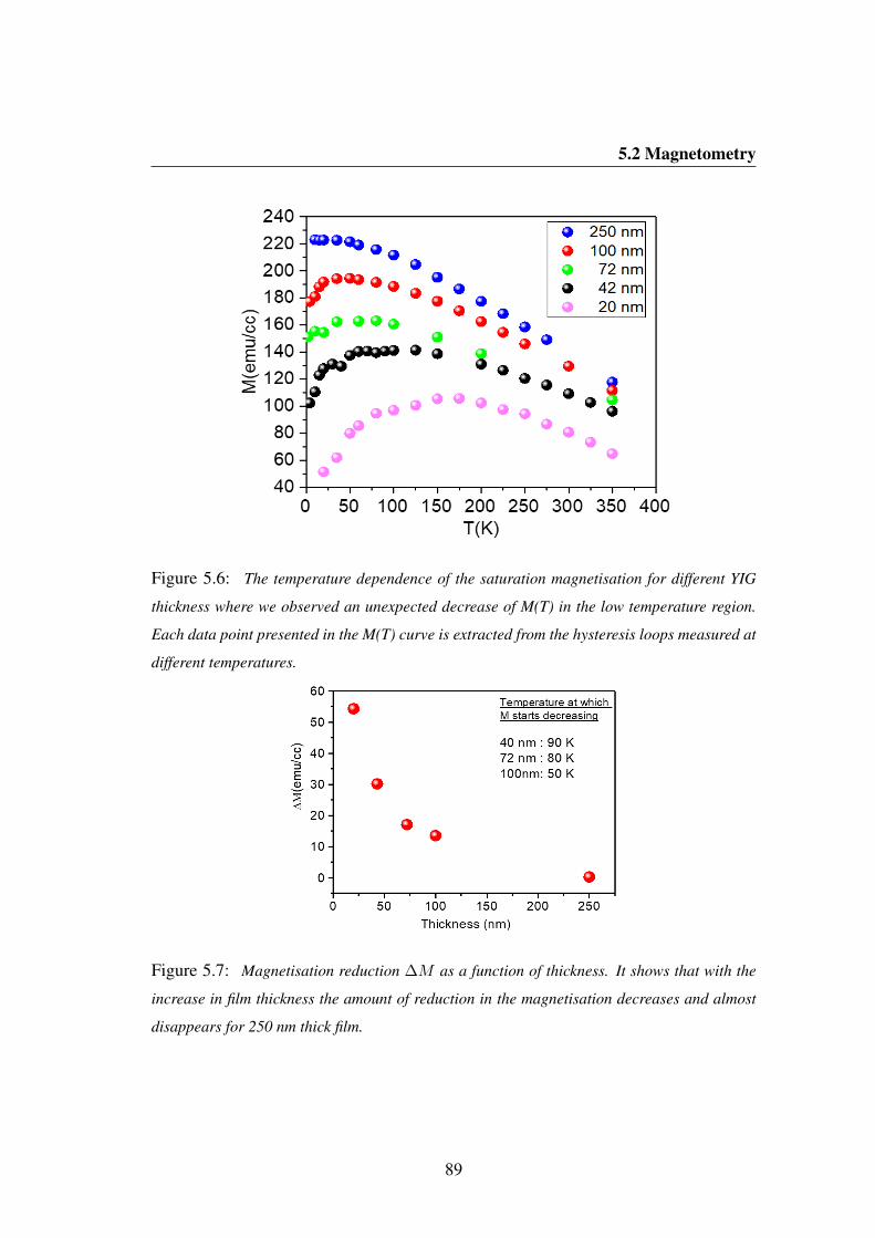
5.2 Magnetometry
Figure 5.6: The temperature dependence of the saturation magnetisation for different YIG
thickness where we observed an unexpected decrease of M(T) in the low temperature region.
Each data point presented in the M(T) curve is extracted from the hysteresis loops measured at
different temperatures.
Figure 5.7: Magnetisation reduction ∆M as a function of thickness. It shows that with the
increase in film thickness the amount of reduction in the magnetisation decreases and almost
disappears for 250 nm thick film.
89

5.2 Magnetometry
YIG layer at the interface between GGG and YIG. Our fit to the x-ray reflectivity
curve gives an estimate of Gd diffusion region thickness of about 6 nm at the inter-
face. Also from the magnetometry data at room temperature, we obtained the value of
dead layer thickness, which is 6 nm (fig.5.3b, section 5.2.1). The magnetic behaviour
of Gd sub-lattice has a strong temperature dependence. It is well known that Gd in
GdIG orders antiparallel at low temperature and dominates the magnetic behaviour.
The ordering temperature of Gd spins is 65-85 K in GdIG, due to which as the temper-
ature is reduced, the magnetization of the Gd sub-lattice strongly increases and aligns
antiparallel to the net magnetic moment of YIG.
So, our interpretation for the magnetisation suppression in YIG at lower temper-
ature is that the Gd-spins in the Gd-diffused region aligning antiparallel and plays
the dominating role to lower the net magnetization value in YIG near the interface.
As indicated in figure 5.7, one can also see that with the increase in film thickness,
the amount of reduction in the magnetisation (∆M) decreases. This is because the
thickness of Gd-diffused region forming at the bottom remains nearly the same but
the thickness of the YIG layer increases. So for the thicker film, the magnetization
of YIG starts dominating and the net cancellation by Gd spins gets reduced at lower
temperature. This reduction in magnetisation almost disappears for 250 nm thick YIG
film.
Next we deposited a very thin sample of 10 nm YIG on GGG, with the assump-
tion that we could measure mainly the effect of Gd-spins diffused into the YIG from
GGG after annealing. Figure 5.8a shows the temperature dependence magnetisation
data for a 10 nm thick YIG film. This is a very important result which highlights the
role of Gd spins at the YIG/GGG interface. This M(T) curve clearly shows a com-
pensation point around 100 K. This region is near to the ordering temperature of Gd
spins, indicating that the Gd magnetic sublattice dominates at lower temperatures. In
GdIG (Gd3Fe5O12), there are three magnetic sublattices: Gd3+(c sites ), Fe3+ (a sites),
and Fe3+ (d sites) [163] (figure 5.8b). Above the compensation temperature Tcomp (T
> Tcomp), the magnetic behaviour is mainly due to the two Fe sub-lattices which are
90

5.2 Magnetometry
Figure 5.8: (a) Temperature dependence of magnetisation of 10 nm thick YIG. (b) Schematic
of three magnetic sublattices in GdIG. It shows the alignment of each sublattice below and
above the compensation temperature Tcomp [162]. Due to strong temperature dependence of
the Gd sub-lattice, it dominates the magnetic behaviour for T <Tcomp, whereas for T >Tcomp
the magnetic behaviour is mainly caused by the antiferromagnetic coupling between Fe sub-
lattices at a and d sites. (c) The temperature dependence magnetisation curve for varying Gd
concentration, which shows 40% Gd doping corresponds to 100 K compensation temperature
[158].
strongly coupled via antiferromagnetic superexchange with a Neel temperature TN =
550 K. As the temperature decreases, the magnetization of the Gd sub-lattice strongly
91
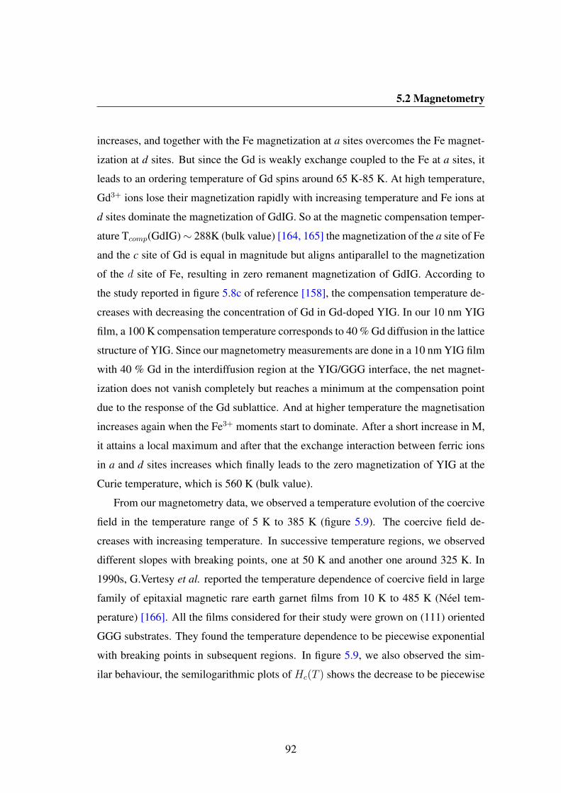
5.2 Magnetometry
increases, and together with the Fe magnetization at a sites overcomes the Fe magnet-
ization at d sites. But since the Gd is weakly exchange coupled to the Fe at a sites, it
leads to an ordering temperature of Gd spins around 65 K-85 K. At high temperature,
Gd3+ ions lose their magnetization rapidly with increasing temperature and Fe ions at
d sites dominate the magnetization of GdIG. So at the magnetic compensation temper-
ature Tcomp(GdIG)∼ 288K (bulk value) [164, 165] the magnetization of the a site of Fe
and the c site of Gd is equal in magnitude but aligns antiparallel to the magnetization
of the d site of Fe, resulting in zero remanent magnetization of GdIG. According to
the study reported in figure 5.8c of reference [158], the compensation temperature de-
creases with decreasing the concentration of Gd in Gd-doped YIG. In our 10 nm YIG
film, a 100 K compensation temperature corresponds to 40 % Gd diffusion in the lattice
structure of YIG. Since our magnetometry measurements are done in a 10 nm YIG film
with 40 % Gd in the interdiffusion region at the YIG/GGG interface, the net magnet-
ization does not vanish completely but reaches a minimum at the compensation point
due to the response of the Gd sublattice. And at higher temperature the magnetisation
increases again when the Fe3+ moments start to dominate. After a short increase in M,
it attains a local maximum and after that the exchange interaction between ferric ions
in a and d sites increases which finally leads to the zero magnetization of YIG at the
Curie temperature, which is 560 K (bulk value).
From our magnetometry data, we observed a temperature evolution of the coercive
field in the temperature range of 5 K to 385 K (figure 5.9). The coercive field de-
creases with increasing temperature. In successive temperature regions, we observed
different slopes with breaking points, one at 50 K and another one around 325 K. In
1990s, G.Vertesy et al. reported the temperature dependence of coercive field in large
family of epitaxial magnetic rare earth garnet films from 10 K to 485 K (Neel tem-
perature) [166]. All the films considered for their study were grown on (111) oriented
GGG substrates. They found the temperature dependence to be piecewise exponential
with breaking points in subsequent regions. In figure 5.9, we also observed the sim-
ilar behaviour, the semilogarithmic plots of Hc(T ) shows the decrease to be piecewise
92
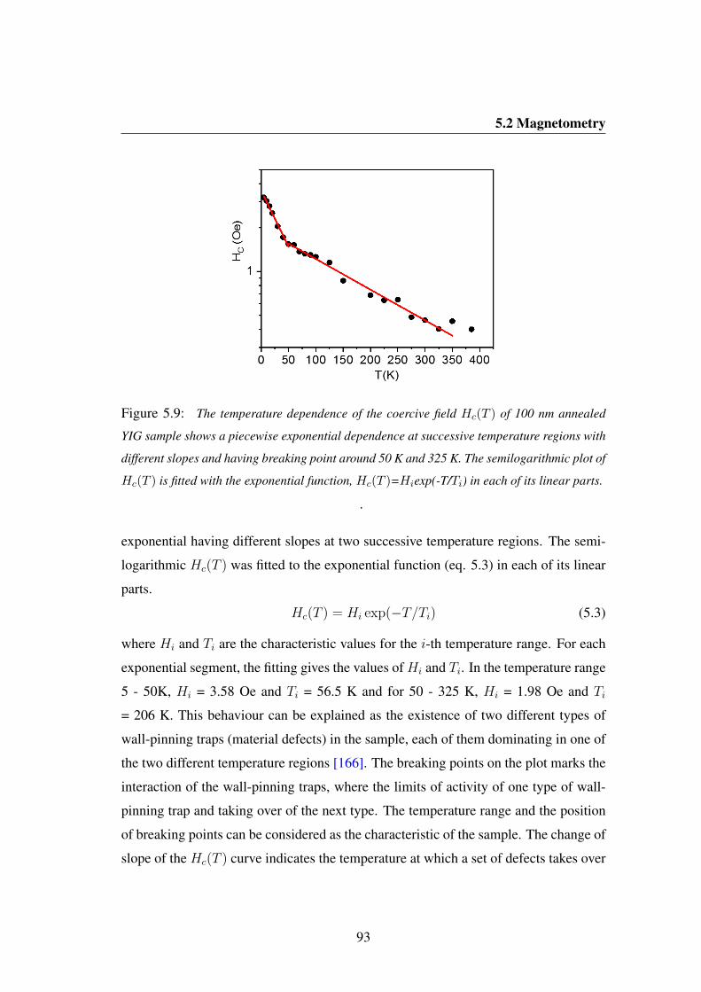
5.2 Magnetometry
Figure 5.9: The temperature dependence of the coercive field Hc(T ) of 100 nm annealed
YIG sample shows a piecewise exponential dependence at successive temperature regions with
different slopes and having breaking point around 50 K and 325 K. The semilogarithmic plot of
Hc(T ) is fitted with the exponential function, Hc(T )=Hiexp(-T/Ti) in each of its linear parts.
.
exponential having different slopes at two successive temperature regions. The semi-
logarithmic Hc(T ) was fitted to the exponential function (eq. 5.3) in each of its linear
parts.
Hc(T ) = Hi exp(−T/Ti) (5.3)
where Hi and Ti are the characteristic values for the i-th temperature range. For each
exponential segment, the fitting gives the values of Hi and Ti. In the temperature range
5 - 50K, Hi = 3.58 Oe and Ti = 56.5 K and for 50 - 325 K, Hi = 1.98 Oe and Ti
= 206 K. This behaviour can be explained as the existence of two different types of
wall-pinning traps (material defects) in the sample, each of them dominating in one of
the two different temperature regions [166]. The breaking points on the plot marks the
interaction of the wall-pinning traps, where the limits of activity of one type of wall-
pinning trap and taking over of the next type. The temperature range and the position
of breaking points can be considered as the characteristic of the sample. The change of
slope of the Hc(T ) curve indicates the temperature at which a set of defects takes over
93
5.2 Magnetometry
the dominant role in the domain wall coercivity from the previous set of defects. The
decrease of Hc(T ) is less rapid at higher temperatures, which is most probably due to
the existence of different sets of mutually nonequivalent wall-pinning defects in the
sample. A large number of rare-earth garnet films demonstrated similar behaviour of
piecewise exponential dependence of coercive field with temperature, resulting from
the mutual interaction of wall-pinning traps [166, 167].
5.2.2.1 YIG/Pt hybrid structures
For our spin pumping and current induced FMR experiments, we used YIG/Pt bilayer
structures, so it is crucial to check the magnetometry results after deposition of Pt on
YIG by DC sputtering. For YIG/Pt hybrid structures, the obtained SQUID magneto-
metry results for the YIG layer remain unchanged qualitatively and quantitatively, as
shown in figure 5.10.
Figure 5.10: (a) Hysteresis loops before (red curve) and after deposition of 10 nm Pt (blue
curve) on 40 nm YIG films. (b) Temperature dependence of magnetisation for the same YIG
(40 nm) and YIG(40 nm)/Pt(10 nm) hybrid structures which shows the same magnetisation
reduction at low temperature.
94
5.2 Magnetometry
5.2.3 Effect of Piranha etching on magnetization
In this section our aim is to get confirmation about the location of magnetically dead
layer near the YIG/GGG interface. For this we analysed our samples before and after
etching. YIG samples were treated with Piranha solution (section 4.4) under same
conditions and the etching time was kept constant.
To study the effect of etching, the magnetisation of the samples was measured
at room temperature using a magnetometer. We observed that etching leads to the
removal of a magnetically active layer from the top surface in addition to the contam-
ination, leading to a decrease in the magnetic moment in each sample after etching, as
shown in figure 5.11a and b. For the 40 nm sample, before etching the moment, m =
3.3 x 10⁻⁴ emu and after etching, thickness of YIG is 34 nm and the moment, m1 =
2.7 x 10⁻⁴ emu. Hence, 6 nm reduction in thickness corresponds to 18% decrease in
magnetic moment after etching. For an unetched 20 nm sample, m = 1.2 x 10⁻⁴ emu
and after etching m1 = 8.71 x 10⁻⁵ emu. So, a 27% decrease in the magnetic moment
corresponds about 8 nm reduction in thickness. These values are an approximate as
we should note that there is an effect of Gd at the interface in each film which we
discovered later at the end of our study.
After etching, one of the samples was measured in the temperature range of 1.8 K
to 385 K to get the temperature dependence of the magnetisation. If we compare the
M(T) results before etching (42 nm YIG) and after etching (35 nm YIG ), one can still
observe the same downturn of magnetisation at lower temperature (figure 5.12). This
is a good indication of the presence of diffused dead layer at the YIG/GGG interface.
Also we found that the etching removes magnetically active layer from the top, and
hence the magnetisation gets reduced, so we did not continue this piranha etching
process anymore.
95

5.2 Magnetometry
Figure 5.11: Moment versus applied field curve before (blue curves) and after etching (red
curve) of 40 nm (a) and 20 nm (b) thick YIG films. This shows degradation of magnetic moment
after etching and hence removing an active layer from the top surface of YIG. For the 40 nm
sample, the moment decreased by 18% after etching whereas for 20 nm thick YIG it shows 27%
decrease.
Figure 5.12: Temperature dependence of the saturation magnetisation of 42 nm thick YIG be-
fore (blue dotted curves) and after Piranha etching (red dotted curves) where below 100K there
is a reduction in M(T). The downturn behaviour is same in both cases but it is quantitatively
different.
96

5.3 Polarised neutron reflectivity measurements
5.3 Polarised neutron reflectivity measurements
To get more information of the magnetic behaviour and further confirmation about the
magnetization downturn in this complex material YIG, a depth-resolved technique is
required. Polarised Neutron Reflectivity (PNR) technique, is ideally suited for these
measurements. The specular reflectivity of spin polarized neutrons depends on the
depth profile of the sample magnetization parallel to the applied field as well as the
depth profile of the nuclear composition. The YIG samples were taken to the Polar-
ised Neutron Reflectometer, POLREF, at the ISIS neutron spallation source, Ruther-
ford Appleton Laboratory for the temperature dependent polarised neutron reflectivity
(PNR) measurements. By using a GMW electromagnet, the samples were magnetised
in a field of 300 mT, far in excess of the required field to saturate the sample. For
neutron reflectivity data, a neutron spin flipper was used to record both the spin up
and spin down neutrons. The samples were then field-cooled to 250 K in a standard
Oxford instruments He flow cryostat at the saturating field, where we performed our
initial PNR measurement. Measurements were then carried on in the following order
at 5 K, 50 K, 80 K and 150 K without changing the applied field at any point, in order
to make the best use of the available counting time. The dimension of the samples
was 20 mm x 20 mm on a 0.5 mm thick GGG substrate. The 80 nm and 10 nm thick
YIG samples are used for these measurements. It would seem that the room temper-
ature magnetic properties of YIG do not reveal any influence of the Gd-diffused layer
but, with decrease in temperature, the magnetic ordering of the Gd-diffused layer takes
place which is immediately evident in the magnetisation.
Figure 5.13 shows the spin-polarised neutron refectivity data (left hand column)
and spin assymetry curves (right hand column) along with their fits as a function of
scattering vector qz for a 80 nm thick YIG film at 5 K, 50 K, 80 K, 150 K and 250 K.
From the reflectivity data we derived the spin asymmetry (SA) using the equation:
SA = I↑ − I↓I↑ + I↓
(5.4)
where I↑ and I↓ refer to the neutron spin reflectivities with orientation parallel or anti-
97

5.3 Polarised neutron reflectivity measurements
Figure 5.13: Spin-polarised neutron reflectivity data (left hand column) for a 80 nm-thick YIG
film and extracted spin asymmetry data (right hand column) along with their fits as a function
of scattering vector qz at 5 K, 50 K, 80 K, 150 K and 250 K. The solid lines are results from
the simulations showing a good fit to the experimental data.
98

5.3 Polarised neutron reflectivity measurements
Figure 5.14: Schematic of a two layer model approach used for fitting the PNR data of 80 nm
YIG sample in Gen-X. It consists of Gd-doped YIG region of about 6 nm thick at the YIG/GGG
interface.
parallel to the applied magnetic field, respectively. As spin asymmetry is sensitive to
the magnetic component, it represents the reflectivity difference caused by the spin de-
pendent magnetic interaction. The fittings for the reflectivity data and SA are obtained
from simulations done by using Gen-X [168]. For the simulations, we approached
a two layer model for YIG and Gd-doped YIG near the YIG/GGG interface (figure
5.14). In this model, the roughness of the substrate is about 1.2 nm and then a 6-7
nm thick layer of interdiffusion region (Gd-rich YIG) at the YIG/GGG interface. We
note that Gd has a significant neutron absorption cross-section which makes us more
sensitive to it. So, we included this absorption to our model to fit the data accurately.
From the PNR model we obtained the scattering length densities and we plotted
it as a function of distance for different temperatures in figure 5.15a. The z-axis rep-
resents the distance along the vertical direction of the sample, where z = 0 represents
the YIG/GGG interface. The areas under the SLD curves were integrated (βSLD) to
get the integrated SLD as a function of temperature (figure 5.15b). Since the scatter-
ing length densities with magnetic components (ρmag) is directly proportional to the
magnetisation of the sample:
ρmag(z) = C∑i
Ni(z)µi (5.5)
where the summation is over each type of atom in the system, N is the in-plane aver-
age of the number density, µ is the magnetic moment in Bohr magnetons and C is a
99

5.3 Polarised neutron reflectivity measurements
constant. So, the integrated SLD can be converted to a magnetisation (emu/cc) using
the relation: m = βSLD/nC where m is the magnetisation, n is the atomic number
density, and C = 2.853× 10⁻⁹ cm3/emu [169]. From figure 5.15a, one can see that at
250 K, the SLD near z = 0 indicates a region which is paramagnetic but this region be-
comes magnetic and orders anti-parallel to the rest of the YIG as we cooled the sample
down to 5 K: this is indicated by a negative SLD. The total thickness is given by the
Kiessig fringes and the model gives a value of ∼ 6 nm for the Gd-diffusion region
which again agrees well with our x-ray reflectivity data, the superSTEM and the room
temperature magnetic data. Then, we measured the temperature dependence of the
magnetisation M(T) on the sample, from 350 K down to 1.8 K using a SQUID-VSM
in an applied field of 50 mT, and have analysed these in combination with the PNR
data as a function of temperature. The integrated SLD is then plotted together with the
independently measured M(T), as shown in figure 5.16. Both these data show a very
good agreement. We know that the moment in YIG is a result of the antiferromagnetic
superexchange mediated by the O2− between the Fe3+ ions on the octahedral (a sites)
and tetrahedral (d sites) sites. This is the strongest of the interactions, so the Gd-doping
does not change the Curie temperature of YIG. Gd substitution for Y on the c sites and
its antiparallel alignment to the net moment of the a + d sites, leads to magnetization
reduction only at low temperature region. This explains the observed PNR results.
In Gd-doped alloys, it has been reported that when Gd concentration exceeds 24%,
there is a compensation temperature where the total moment passes through zero, and
interestingly, the Gd-YIG system rotates coherently as the compensation temperature
is passed [158]. We note that a clear compensation temperature was observed in our
YIG/GGG system, for 10 nm YIG sample (figure 5.8a), and the 100 K compensation
temperature agrees well with that found for a 40% Gd doped YIG film as shown in
ref. [158]. For this 10 nm sample, PNR measurements were done in the same way as
for the 80 nm film. But using the same two-layer model approach, it was difficult to
fit the PNR data in Gen-X. This is most likely due to the wide Gd-rich diffused region
and continuous composition gradient within the sample. Figure 5.17a shows the spin
100

5.3 Polarised neutron reflectivity measurements
Figure 5.15: We show (a) the scattering length density (SLD) as a function of distance through
the 80 nm sample (z = 0 is the GGG/YIG interface) and temperature. Clearly visible (between
0 and 50 A) is the increase in the Gd moment ordering antiparallel to the YIG moment as the
temperature is reduced from 250 K to 5 K. (b) Integrated SLD as a function of temperature.
Figure 5.16: The temperature dependence of the magnetisation for the same 80 nm YIG
sample measured by SQUID magnetometry. The points overlaid are the integrated SLD which
shows a convincing correlation between the two measurements.
asymmetry curve for different temperatures for 10 nm YIG.
For each temperature, the amplitude of spin asymmetry (∆SA) at qz ≈ 0.047 A−1
101
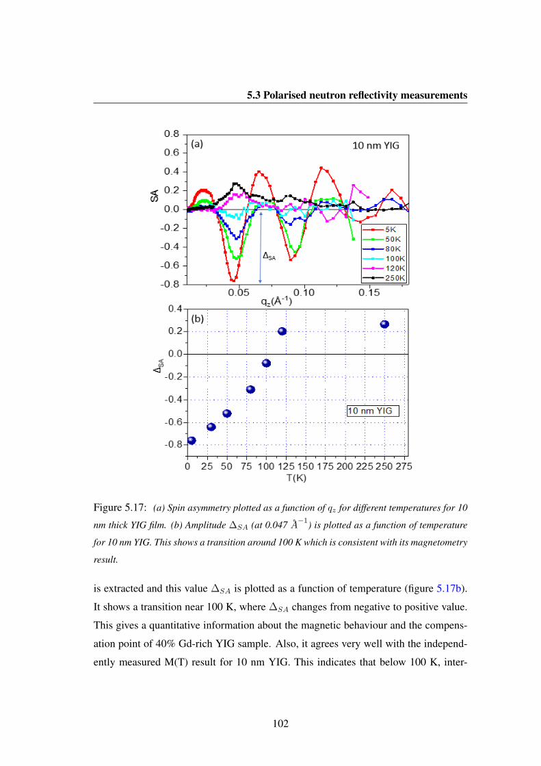
5.3 Polarised neutron reflectivity measurements
Figure 5.17: (a) Spin asymmetry plotted as a function of qz for different temperatures for 10
nm thick YIG film. (b) Amplitude ∆SA (at 0.047 A−1) is plotted as a function of temperature
for 10 nm YIG. This shows a transition around 100 K which is consistent with its magnetometry
result.
is extracted and this value ∆SA is plotted as a function of temperature (figure 5.17b).
It shows a transition near 100 K, where ∆SA changes from negative to positive value.
This gives a quantitative information about the magnetic behaviour and the compens-
ation point of 40% Gd-rich YIG sample. Also, it agrees very well with the independ-
ently measured M(T) result for 10 nm YIG. This indicates that below 100 K, inter-
102

5.3 Polarised neutron reflectivity measurements
action of neutron magnetic moment with the magnetisation of the sample is different
from that above 100 K.
With the information obtained from the PNR results of 80 nm YIG, we developed
a mean field model for the magnetisation as function of temperature M(T) for the
YIG/GGG system based on two layers: YIG and Gd-rich YIG layer, where:
M(T ) = MyB(Jy, zy) +MgB(Jg, zg) (5.6)
where B is the Brillouin function, My and Mg are the saturation magnetisations of the
YIG and Gd-rich YIG layers respectively. zy and zg are defined as
zy = gµBHyJykBT
(t− tgt
)Mm(T ) (5.7)
and
zg = gµBHgJgkBT
(tgt
)Mm(T ) (5.8)
where t is the thickness of the total layer, tg is the thickness of the Gd-doped region,
which we considered to be 6 nm for all samples, Hy and Hg are the Weiss fields for
YIG and Gd-doped YIG, and are fitting parameters. Jy and Jg are the spin quantum
numbers for the two layers taken to be: Jy = 5/2 and Jg = 7/2. Mm(T ) is the
measured value of the magnetisation.
Figure 5.18 shows the temperature dependence of the saturation magnetisation with
their fits for different thickness of the YIG. In the left hand column are the M(T)
measurements for various thicknesses and the solid line represents the fit using the
two-layer mean field model. The right hand column shows the magnetisations for
the two individual layers (YIG in red and Gd-doped YIG in green) where a negative
sign indicates an antiparallel moment. One can see that the simple two-layer model
fits all the data consistently for all samples with a common Gd region of 6 nm. The
saturation magnetisation of YIG obtained from the fit are close to the accepted value.
We have considered a fixed thickness of 6 nm for Gd-layer, but the behaviour of the
Gd-layer varies slightly among the samples, this difference is due to the Weiss field
fitting parameter. We have taken a constant thickness of the Gd-layer to maintain
103

5.3 Polarised neutron reflectivity measurements
Figure 5.18: Temperature dependence of magnetisation for a series of YIG film thickness.
The left hand column shows the M(T) data where the line is a fitting to the data using a mean
field approach. The model uses two magnetic layers: YIG and Gd-doped YIG. The right hand
column shows the magnetisation for the individual layers: YIG in red and Gd-doped YIG in
green. The negative values for the Gd-doped YIG indicates it is antiparallel to the YIG. M(T)
data fitting is done by B.J.Hickey.
104
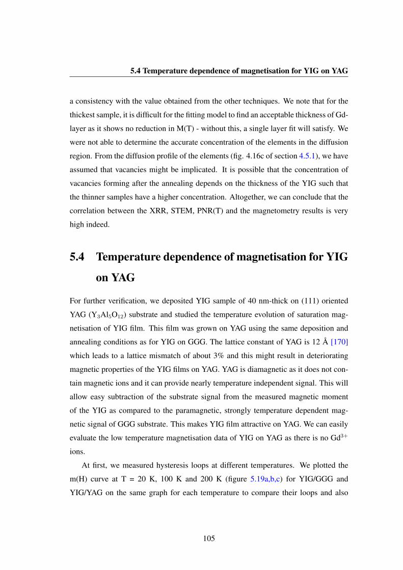
5.4 Temperature dependence of magnetisation for YIG on YAG
a consistency with the value obtained from the other techniques. We note that for the
thickest sample, it is difficult for the fitting model to find an acceptable thickness of Gd-
layer as it shows no reduction in M(T) - without this, a single layer fit will satisfy. We
were not able to determine the accurate concentration of the elements in the diffusion
region. From the diffusion profile of the elements (fig. 4.16c of section 4.5.1), we have
assumed that vacancies might be implicated. It is possible that the concentration of
vacancies forming after the annealing depends on the thickness of the YIG such that
the thinner samples have a higher concentration. Altogether, we can conclude that the
correlation between the XRR, STEM, PNR(T) and the magnetometry results is very
high indeed.
5.4 Temperature dependence of magnetisation for YIG
on YAG
For further verification, we deposited YIG sample of 40 nm-thick on (111) oriented
YAG (Y3Al5O12) substrate and studied the temperature evolution of saturation mag-
netisation of YIG film. This film was grown on YAG using the same deposition and
annealing conditions as for YIG on GGG. The lattice constant of YAG is 12 A [170]
which leads to a lattice mismatch of about 3% and this might result in deteriorating
magnetic properties of the YIG films on YAG. YAG is diamagnetic as it does not con-
tain magnetic ions and it can provide nearly temperature independent signal. This will
allow easy subtraction of the substrate signal from the measured magnetic moment
of the YIG as compared to the paramagnetic, strongly temperature dependent mag-
netic signal of GGG substrate. This makes YIG film attractive on YAG. We can easily
evaluate the low temperature magnetisation data of YIG on YAG as there is no Gd3+
ions.
At first, we measured hysteresis loops at different temperatures. We plotted the
m(H) curve at T = 20 K, 100 K and 200 K (figure 5.19a,b,c) for YIG/GGG and
YIG/YAG on the same graph for each temperature to compare their loops and also
105
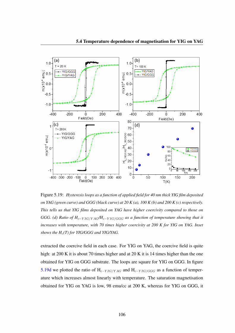
5.4 Temperature dependence of magnetisation for YIG on YAG
Figure 5.19: Hysteresis loops as a function of applied field for 40 nm thick YIG film deposited
on YAG (green curve) and GGG (black curve) at 20 K (a), 100 K (b) and 200 K (c) respectively.
This tells us that YIG films deposited on YAG have higher coercivity compared to those on
GGG. (d) Ratio of Hc−Y IG/Y AG/Hc−Y IG/GGG as a function of temperature showing that it
increases with temperature, with 70 times higher coercivity at 200 K for YIG on YAG. Inset
shows the Hc(T) for YIG/GGG and YIG/YAG.
extracted the coercive field in each case. For YIG on YAG, the coercive field is quite
high: at 200 K it is about 70 times higher and at 20 K it is 14 times higher than the one
obtained for YIG on GGG substrate. The loops are square for YIG on GGG. In figure
5.19d we plotted the ratio of Hc−Y IG/Y AG and Hc−Y IG/GGG as a function of temper-
ature which increases almost linearly with temperature. The saturation magnetisation
obtained for YIG on YAG is low, 98 emu/cc at 200 K, whereas for YIG on GGG, it
106
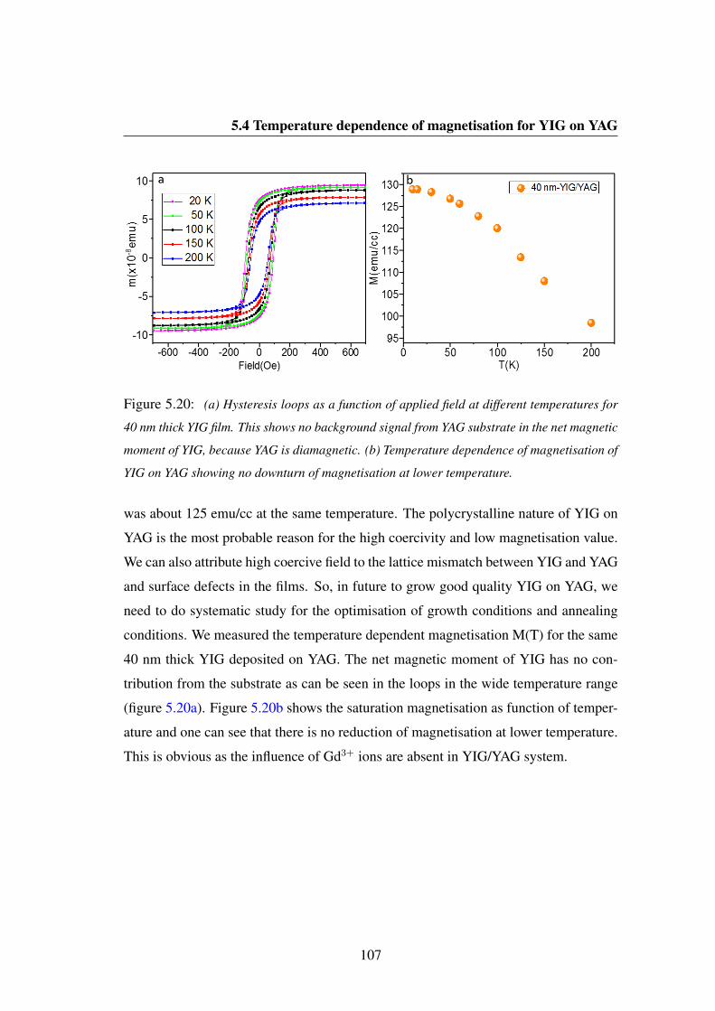
5.4 Temperature dependence of magnetisation for YIG on YAG
Figure 5.20: (a) Hysteresis loops as a function of applied field at different temperatures for
40 nm thick YIG film. This shows no background signal from YAG substrate in the net magnetic
moment of YIG, because YAG is diamagnetic. (b) Temperature dependence of magnetisation of
YIG on YAG showing no downturn of magnetisation at lower temperature.
was about 125 emu/cc at the same temperature. The polycrystalline nature of YIG on
YAG is the most probable reason for the high coercivity and low magnetisation value.
We can also attribute high coercive field to the lattice mismatch between YIG and YAG
and surface defects in the films. So, in future to grow good quality YIG on YAG, we
need to do systematic study for the optimisation of growth conditions and annealing
conditions. We measured the temperature dependent magnetisation M(T) for the same
40 nm thick YIG deposited on YAG. The net magnetic moment of YIG has no con-
tribution from the substrate as can be seen in the loops in the wide temperature range
(figure 5.20a). Figure 5.20b shows the saturation magnetisation as function of temper-
ature and one can see that there is no reduction of magnetisation at lower temperature.
This is obvious as the influence of Gd3+ ions are absent in YIG/YAG system.
107

5.5 Conclusion
5.5 Conclusion
In this chapter, we performed a systematic study of the magnetic properties of nm-thick
YIG films on the GGG substrate over the wide temperature range. We have adopted
a multi-technique approach to investigate the dead layer thickness and low temper-
ature magnetisation suppression. The magnetic properties of YIG on (111) oriented
GGG substrate was measured extensively using magnetometry and polarised neutron
reflectivity. Measuring the magnetic moment of YIG at low temperatures is quite chal-
lenging due to the paramagnetism induced by the Gd3+ ions from the GGG substrate,
that can easily swamp the magnetic signal from thin YIG films. Our interesting results
of YIG on GGG, emphasizing the low-temperature magnetic data highlight the essen-
tial role of Gd-diffused interlayer in the temperature dependence of the magnetization
of YIG. The results obtained from the room temperature magnetometry show that our
YIG films are of high quality with very low coercivity and a saturation magnetisation
close to the bulk value (140 emu/cc). We identified a 6 nm thick magnetically dead
layer at the YIG/GGG interface. We did the surface cleaning of YIG by Piranha etch-
ing to remove organic contamination from the top surface. This contamination is most
likely coming from the ex-situ annealing and air exposure. We found that the piranha
etching removes the active layer of YIG from the top surface along with the contam-
ination, resulting in a decreased saturation magnetisation of YIG films after etching.
Temperature dependence of the magnetisation in an etched YIG sample also confirms
the existence of dead layer at the interface. We have also shown that deposition of Pt
on YIG in YIG/Pt bilayer films does not alter the magnetisation value of YIG.
The temperature dependence of magnetisation in YIG/GGG system revealed an
reduction in magnetisation at low temperature. To complement this result, we per-
formed temperature dependent polarised neutron reflectivity experiment. This gives
a very high correlation between the magnetometry (SQUID-VSM) and PNR results.
We proposed a simple two-layer model which fits all the M(T) data consistently for
different thickness of YIG samples with a common Gd region of 6 nm. Finally, our
M(T) results on YIG on YAG substrate which shows no reduction of magnetisation
108

5.5 Conclusion
at low temperature, further confirms the role of Gd3+ ions in the YIG/GGG system.
The magnetic quality of YIG on YAG deteriorates: low saturation magnetisation and
high coercivity. So. it is necessary to optimise the growth and annealing conditions for
getting high quality YIG on YAG.
Our most important finding is ∼ 6 nm Gd-interdiffusion region at the YIG/GGG
interface, which is paramagnetic at room temperature and orders antiparallel to YIG
at low temperatures. This interfacial origin of the magnetization suppression affect
the properties of YIG and should be taken into account for studies of fundamental
magnetic phenomena such as magnetization dynamics, spin pumping effect and STT
effect which demands thin films in the region of 10 - 20 nm for YIG-based spintronics
devices.
109
CHAPTER 6
Ferromagnetic resonance properties of
nm-thick YIG films
110
6.1 Introduction
6.1 Introduction
In the magnonics community, researchers are aiming to make pure spin currents as
a unique information carrier. For this, YIG is an excellent magnetic material which
has been widely used for studying high frequency magnetization dynamics due to its
extremely small magnetization damping, 5 x 10⁻⁵, high Curie temperature and high
chemical stability [35, 40, 171]. Because of its unique properties, in the mid-twentieth
century bulk YIG crystal was the standard material for ferromagnetic resonance stud-
ies. The emergence of YIG-based spintronic devices requires high quality ultrathin
YIG films and understanding of the magneto-dynamic properties in nm-thick YIG
films for experiments concerning spin wave propagation. In recent years, YIG/Pt
heterostructures have attracted considerable interest. Since YIG is an insulator, dir-
ect injection of a spin current from the YIG into the Pt layer is not possible. Spin
current injection in the adjacent Pt layer can be possible only by the spin pumping
phenomenon, realized through exchange interaction between localized electrons in the
YIG film and conduction electrons in the Pt layer. Platinum is the most favourable
material due to its high spin-orbit coupling which is necessary for the conversion of
spin currents into electrical currents by the ISHE. Spin pumping is an interfacial ef-
fect, so good interface quality is necessary to achieve high spin pumping efficiency. It
also depends on the spin mixing conductance which can be determined from the Gil-
bert damping. Spin pumping in a bilayer structure is revealed by the increased Gilbert
damping factor, which depends on the temperature and the defects present in a sample
[172].
In this work, we investigated the FMR properties and particularly the damping
behaviour of RF sputtered nm-thick YIG films using ferromagnetic resonance (FMR)
technique. At first we report the thickness dependence of FMR properties for YIG
films. We performed temperature dependent FMR measurements in YIG and YIG/Pt
samples to extract the behaviour of the Gilbert damping. For the implementation of
spin transfer torque (STT) devices using YIG, it is important to understand the nature of
the torque acting on the YIG induced by the charge current in metal layers in YIG/metal
111
6.2 Thickness dependent FMR properties
system. So, we performed current-induced FMR (CI-FMR) experiment in YIG/metal
bilayer structures to characterise and quantify the current induced torque. In this work,
we used C60 molecules, due to its structural simplicity and robustness to make YIG/C60
heterostructures. It has been found that C60 has higher spin-orbit interaction due to the
curvature of the molecule compared to other carbon allotropes [173]. We investigated
the dynamic properties of YIG/C60 structures to find the effect of C60 molecules on
the damping of YIG. With C60 on top of YIG, we expect to realise spin pumping
from YIG into the molecules. We also performed PNR-FMR experiments in which
we combined the FMR technique with polarised neutron reflectivity, to detect spin
pumping in YIG/Pt manifested as spin asymmetry.
6.2 Thickness dependent FMR properties
We performed in-plane FMR measurements for different thicknesses of YIG nano
films. The samples used for the FMR measurements are about 4 x 4 mm2. The mag-
netization dynamics are excited by applying an alternating microwave field oriented
perpendicular to the external in-plane bias field. At ferromagnetic resonance condi-
tion, the dependence of ferromagnetic resonance frequency on the field follows the
Kittel formula [160] :
f = (µ0γ/2π)√Hres(Hres +Meff ) (6.1)
where Hres is the magnetic field at the resonance condition for a given fixed frequency
and µ0 is the vacuum permeability. By fitting the field dependence of the resonance
frequency with the Kittel formula we can obtain the value of gyromagnetic ratio γ
and the effective magnetization Meff for our nm thick YIG films. The effective mag-
netization is the sum of saturation magnetization Ms and the anisotropy field Hani.
Therefore, the effective magnetization takes the out-of-plane anisotropy into account.
We can calculate the anisotropy constant Ku1 by using the relation [86]:
112

6.2 Thickness dependent FMR properties
Ku1 = µ0HaniMs
2 = µ0(Ms −Meff )Ms
2 (6.2)
Figure 6.1: (a) Ferromagnetic resonance spectra of the absorption for 80 nm YIG film at fre-
quencies of 5, 6, 7 and 8 GHz measured at room temperature using lock-in detection technique.
(b) A typical FMR data at 5 GHz showing the Lorentzian absorption line with its fit which gives
resonance field Hres = 136.5 mT and linewidth of 1 mT.
The Gilbert damping parameter α can be estimated from the frequency dependence
of FMR linewidth dH by using the relation:
dH = 4παfγµ0
(6.3)
Figure 6.1a shows the typical FMR spectra measured at different frequency (5-8
GHz) using lock-in detection (section 3.8), showing the Lorentzian absorption line and
a typical FMR data at 5 GHz is shown with its Lorentzian fit (figure 6.1b). Data were
measured at room temperature. Dependence of the FMR frequency on the resonance
field for a 80 nm-thick sample is shown in figure 6.2a and the solid line is a Kittel fit
to the experimental data. From this we extracted the value of gyromagnetic ratio and
the effective magnetization. Figure 6.2b shows the evolution of the FMR linewidth
(dH) as a function of frequency. From the linear fit of the frequency dependence of
the FMR linewidth we can extract the value of Gilbert damping parameter of the film.
113

6.2 Thickness dependent FMR properties
Figure 6.2: (a) Dependence of the ferromagnetic resonance frequency on the resonance field
for a 80 nm-thick sample, the solid line (red curve) is a Kittel fit to the experimental data. This
gives a standard value of gyromagnetic ratio 27.2 GHz/T and µ0Meff = 110 ± 2 emu/cc. (b)
FMR linewidth as a function of frequency measured at room temperature. The solid lines are
linear fits to the data. Damping extracted from the slope of the linear fit is 1.61 x 10⁻³.
The Gilbert damping should be proportional to the linewidth while the zero-frequency
offset dH0 along the y-axis is related to the extrinsic contributions to damping, such as
film inhomogeneities and two-magnon scattering.
The results of FMR measurements for different YIG thicknesses are summarised
in Table 6.1. These samples were grown from the new target (Target-B). Here dH0, the
zero-frequency intercept of the FMR linewidth is extracted from the linear fits to the
data (fig. 6.2b), and the damping α is extracted from the slope of the linear fits. The
inhomogenous linewidth broadening dH0 of our films varies between 4 to 6 Oe, which
is comparable to the value of 3 to 6 Oe for 19 nm to 49 nm thick YIG films as reported
in the reference [174]. The linewidth obtained for a set of RF sputtered YIG samples
of 83 nm and 96 nm thick is in the range of 4 to 6 Oe, reported in ref. [64]. The values
obtained for Meff is lower than the saturation magnetization for the bulk YIG (140
emu/cc).
We plotted the thickness dependence of Gilbert damping parameter of our nm-
114
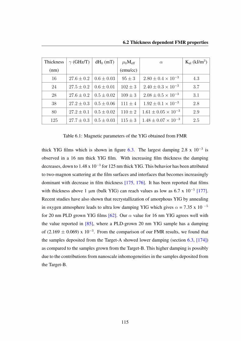
6.2 Thickness dependent FMR properties
Thickness γ (GHz/T) dH0 (mT) µ0Meff α Kul (kJ/m3)
(nm) (emu/cc)
16 27.6± 0.2 0.6± 0.03 95± 3 2.80± 0.4× 10⁻³ 4.324 27.5± 0.2 0.6± 0.01 102± 3 2.40± 0.3× 10⁻³ 3.728 27.6± 0.2 0.5± 0.02 109± 3 2.08± 0.5× 10⁻³ 3.138 27.2± 0.3 0.5± 0.06 111± 4 1.92± 0.1× 10⁻³ 2.880 27.2± 0.1 0.5± 0.02 110± 2 1.61± 0.05× 10⁻³ 2.9125 27.7± 0.3 0.5± 0.03 115± 3 1.48± 0.07× 10⁻³ 2.5
Table 6.1: Magnetic parameters of the YIG obtained from FMR
thick YIG films which is shown in figure 6.3. The largest damping 2.8 x 10⁻³ is
observed in a 16 nm thick YIG film. With increasing film thickness the damping
decreases, down to 1.48 x 10⁻³ for 125 nm thick YIG. This behavior has been attributed
to two-magnon scattering at the film surfaces and interfaces that becomes increasingly
dominant with decrease in film thickness [175, 176]. It has been reported that films
with thickness above 1 µm (bulk YIG) can reach values as low as 6.7 x 10⁻⁵ [177].
Recent studies have also shown that recrystallization of amorphous YIG by annealing
in oxygen atmosphere leads to ultra low damping YIG which gives α = 7.35 x 10 −5
for 20 nm PLD grown YIG films [62]. Our α value for 16 nm YIG agrees well with
the value reported in [85], where a PLD-grown 20 nm YIG sample has a damping
of (2.169 ± 0.069) x 10−3. From the comparison of our FMR results, we found that
the samples deposited from the Target-A showed lower damping (section 6.3, [174])
as compared to the samples grown from the Target-B. This higher damping is possibly
due to the contributions from nanoscale inhomogeneities in the samples deposited from
the Target-B.
115

6.3 Temperature dependence of Gilbert damping in YIG and YIG/Pt
Figure 6.3: Gilbert damping parameter of nanometre thick YIG films as a function of film
thickness. This shows that damping decreases with increase in film thickness. The largest
damping is observed for 16 nm thick film, which is about 2.8 x 10⁻³. Inset shows that α is
proportional to 1/Thickness.
6.3 Temperature dependence of Gilbert damping in YIG
and YIG/Pt
In this study, ferromagnetic resonance properties were measured using coplanar wave-
guide with frequency band (1-20 GHz) by applying in-plane external magnetic field.
The measurements were carried out in the cryogenics system in the temperature range
20 K to 300 K. We used 40 nm YIG and YIG (40 nm)/Pt (10 nm) bilayer samples for
our measurements. This 40 nm thick film showed a RMS surface roughness of about
2 A with (111) crystalline orientation. Before doing the FMR in these films, we meas-
ured the saturation magnetization Ms at room temperature and also its temperature
dependence using SQUID magnetometry (figure 5.10b chapter 5).
The inset of figure 6.4 shows the FMR profile of the 40 nm thick YIG sample
obtained at 9 GHz at 300 K and the solid curve shows the fit to the derivative of
Lorentzian function. In the FMR profile, sometimes we also observed more than a
116

6.3 Temperature dependence of Gilbert damping in YIG and YIG/Pt
Figure 6.4: Dependence of the ferromagnetic resonance frequency on the resonance field for a
40 nm thick YIG sample. The fitted line (red curve) is obtained by using the Kittel formula. The
inset shows a typical FMR lineshape at 9 GHz thus showing the derivative of the Lorentzian
absorption line.
single absorption peak which can be attributed to the standing spin wave modes of the
ultra low damping YIG layers [62]. In order to fit such a FMR profile, one needs to
take the superposition of a few closely separated Lorentzian lines. Fitting of the field
dependence of the FMR resonance frequencies (figure 6.4) using the Kittel equation
6.1, gives the gyromagnetic ratio, γ = 28 GHz/T. From the slope of the linear fit to
the linewidth versus resonance frequencies (figure 6.5), we can extract the damping
parameters (using equation 6.3) for each temperature. For a 40 nm YIG film at 300 K,
the FMR linewidth is about 6 Oe at 9 GHz with a damping constant of (5.4 ± 0.2) x
10−4. At 100 K, the damping is increased by a factor of 3.8. We have observed the
same effect in YIG/Pt samples, when the temperature drops from 300 K to 100 K, the
damping parameter increased by 2.5 times: at 300 K, α = (6.08 ± 0.1) x 10−3 and at
100 K, α = (15.2± 0.2) x 10−3. Damping in our films is significantly smaller than that
of metallic films of similar thickness. Our FMR linewidth is comparable to the value
117
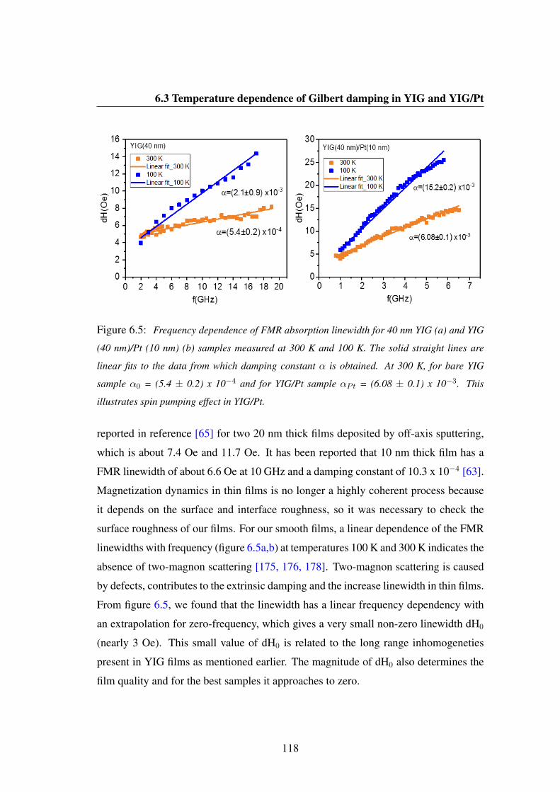
6.3 Temperature dependence of Gilbert damping in YIG and YIG/Pt
Figure 6.5: Frequency dependence of FMR absorption linewidth for 40 nm YIG (a) and YIG
(40 nm)/Pt (10 nm) (b) samples measured at 300 K and 100 K. The solid straight lines are
linear fits to the data from which damping constant α is obtained. At 300 K, for bare YIG
sample α0 = (5.4 ± 0.2) x 10−4 and for YIG/Pt sample αPt = (6.08 ± 0.1) x 10−3. This
illustrates spin pumping effect in YIG/Pt.
reported in reference [65] for two 20 nm thick films deposited by off-axis sputtering,
which is about 7.4 Oe and 11.7 Oe. It has been reported that 10 nm thick film has a
FMR linewidth of about 6.6 Oe at 10 GHz and a damping constant of 10.3 x 10⁻⁴ [63].
Magnetization dynamics in thin films is no longer a highly coherent process because
it depends on the surface and interface roughness, so it was necessary to check the
surface roughness of our films. For our smooth films, a linear dependence of the FMR
linewidths with frequency (figure 6.5a,b) at temperatures 100 K and 300 K indicates the
absence of two-magnon scattering [175, 176, 178]. Two-magnon scattering is caused
by defects, contributes to the extrinsic damping and the increase linewidth in thin films.
From figure 6.5, we found that the linewidth has a linear frequency dependency with
an extrapolation for zero-frequency, which gives a very small non-zero linewidth dH0
(nearly 3 Oe). This small value of dH0 is related to the long range inhomogeneties
present in YIG films as mentioned earlier. The magnitude of dH0 also determines the
film quality and for the best samples it approaches to zero.
118

6.3 Temperature dependence of Gilbert damping in YIG and YIG/Pt
Figure 6.6: Effective magnetization as a function of temperature for YIG (40 nm) (black
dots) and YIG(40 nm)/Pt(10 nm) (red squares) samples. The value of effective magnetization
is extracted from the Kittel fit of FMR data at each temperature. This also shows a downturn
in effective magnetization at lower temperatures.
We noticed that the effective magnetization in YIG shows a decrease with decrease
in temperature, it started reducing after 100 K (figure 6.6), which agrees with the res-
ults of temperature dependence saturation magnetization M(T) SQUID data (figure
5.10b). These behaviour can be attributed to the anti-parallel alignment of the mag-
netic moment in the Gd-doped YIG layer near the YIG/GGG interface, as explained in
chapter 5. For YIG/Pt, Meff (T) also showed a reduction in magnetization but below
60 K. The value of Meff in YIG/Pt is lower than that of YIG sample between 60 K to
300 K, which is in contrast to the M(T) data. This difference is not clearly understood,
so it requires further investigation. It might be possible that there is a spin transfer by
an induced eddy current which is affecting the magnetization dynamics in YIG. We
should repeat the measurements on YIG/Pt samples by varying the YIG thicknesses.
The temperature dependent FMR measurements is done in collaboration with Univer-
sity of Regensburg.
In figure 6.7, we plotted the temperature dependence of the Gilbert damping factor
α for YIG (40 nm) and YIG(40 nm)/Pt(10 nm) samples. From this we observed that the
119
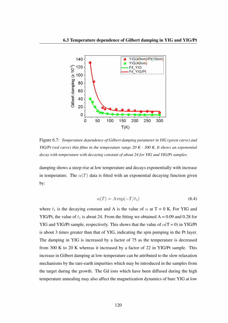
6.3 Temperature dependence of Gilbert damping in YIG and YIG/Pt
Figure 6.7: Temperature dependence of Gilbert damping parameter in YIG (green curve) and
YIG/Pt (red curve) thin films in the temperature range 20 K - 300 K. It shows an exponential
decay with temperature with decaying constant of about 24 for YIG and YIG/Pt samples.
damping shows a steep rise at low temperature and decays exponentially with increase
in temperature. The α(T ) data is fitted with an exponential decaying function given
by:
α(T ) = A exp(−T/t1) (6.4)
where t1 is the decaying constant and A is the value of α at T = 0 K. For YIG and
YIG/Pt, the value of t1 is about 24. From the fitting we obtained A = 0.09 and 0.28 for
YIG and YIG/Pt sample, respectively. This shows that the value of α(T = 0) in YIG/Pt
is about 3 times greater than that of YIG, indicating the spin pumping in the Pt layer.
The damping in YIG is increased by a factor of 75 as the temperature is decreased
from 300 K to 20 K whereas it increased by a factor of 22 in YIG/Pt sample. This
increase in Gilbert damping at low-temperature can be attributed to the slow relaxation
mechanisms by the rare-earth impurities which may be introduced in the samples from
the target during the growth. The Gd ions which have been diffused during the high
temperature annealing may also affect the magnetization dynamics of bare YIG at low
120

6.3 Temperature dependence of Gilbert damping in YIG and YIG/Pt
temperature. There is another possibility of the presence of Fe2+ as impurities which
might have been incorporated during the YIG growth. In 1960s, researchers reported
an increase in linewidth in bulk YIG samples at low temperature due to the impurity
relaxation mechanisms [71, 179–184]. Recently, the increase in linewidth at low tem-
perature has also been observed in 15 nm YIG film deposited by off-axis sputtering
[185]. But it is not universal as Haidar et al. have observed an increase in damping
coefficient in PLD-grown YIG films (30-170 nm) that increases by approximately a
factor of 2 as the temperature increases from 8 K to room temperature [58]. Accord-
ing to them, this temperature dependence is due to the films itself which may consist
of rare-earth ions due to the target impurities. From the results in our nm-thick YIG
samples, we can conclude that low temperature experiments in thin YIG films require
very high purity material and so there is always a scope for the optimization of the
growth and annealing conditions.
For the YIG/Pt thin film, the effective damping parameter is greater than the damp-
ing of bare YIG film. This is due to the spin pumping from the magnetisation dynamics
in the YIG to the normal metal Pt. At 300 K, for the bare YIG sample, damping factor
α0 = (5.4 ± 0.2) x 10−4 whereas for Pt (10 nm) covered YIG sample, αPt = (6.08 ±0.1) x 10−3. The spin mixing conductance g↑↓ is related to the change of the Gilbert
damping, ∆α = αPt - α0 as
g↑↓ = 4πMsd∆αgµB
(6.5)
Taking d = 40 nm as thickness of YIG, we obtained spin mixing conductance, g↑↓ =
(1.6 ± 0.3) x 1019 m−2 for this particular sample. Our spin-mixing conductance is
three orders of magnitude greater than the one reported for YIG(1.3 µm)/Pt(10 nm)
(g↑↓ = 3 x 10¹⁶ m−2 ) system in ref.[35], in which YIG was deposited by liquid phase
epitaxy. It has been found that the spin mixing conductance lies in the range of 5 x
1018 m−2 to 15 x 1018 m−2 for a series of 20 nm YIG/Pt bilayer samples with varying
Pt thicknesses [186]. Lustikova et al. has reported a value of (2.0 ± 0.2) x 1018
m−2 for RF sputtered YIG(96 nm)/Pt(14 nm) sample [64], so our value is greater by
121

6.4 Current induced FMR in YIG/Pt bilayer
one order of magnitude. Our g↑↓ value is smaller compared to 3.43 x 10¹⁹ m−2 for
YIG(2.1 µm)/Pt(10 nm) system where the YIG surface was treated with a combination
of piranha etching and O+/Ar+ plasma [51]. This surface treatment removes the water
as well as dirt, and also the organic contamination from the sample surface. In this
work they have shown a strong dependence of the spin pumping efficiency on the
interface condition of YIG/Pt bilayer films. The maximum value is reported in ref.[53]
for YIG (8 µm)/Pt(8 nm) sample where g↑↓ = 4.8 x 10²⁰ m−2. In future, we should
consider the surface processing of YIG before Pt deposition to get better interface
quality for the realization of efficient spin pumping devices.
6.4 Current induced FMR in YIG/Pt bilayer
In this section, our aim is to investigate and quantify the current induced torque in
YIG/Pt bilayer structures by using current induced FMR (CI-FMR). Due to the spin
Hall effect (section 2.6), an oscillating charge current applied to the metal layer can be
converted to a transverse spin current, which can manipulate the magnetization dynam-
ics in the magnetic insulator by an oscillating spin transfer torque (STT). The charge
current in the metal layer generates the Oersted field which also contributes in driving
the magnetization precession. We applied a microwave current in the metal attached
to our YIG layer and an in plane external magnetic field. At resonance, an output
DC voltage is generated simultaneously due to the spin rectification and spin pumping
mechanisms. From the lineshape and symmetry of the DC voltage we understood the
kind of the torque acting on the YIG. The lineshape and the symmetry of the resonance
in the DC voltage depend on the driving mechanisms of magnetization precession and
how the DC voltage is generated, which we discussed in section 2.5.
For CI-FMR experiment we used YIG/Pt(4.2 nm) bilayer structures with different
YIG thickness. By using optical lithography and argon ion milling, we patterned our
samples into 5 x 50 µm2 bars. To make the contact electrodes a layer of 5 nm Cr/50
nm Au was evaporated. For the measurements, each bar was placed on a low-loss
122

6.4 Current induced FMR in YIG/Pt bilayer
Figure 6.8: (a) FMR spectra of CI-FMR at 4 - 8 GHz is Lorentzian consisting of symmetric
and antisymmetric components. (b) Resonance frequency f as a function of the resonant field
µ0Hres, fitted with in-plane Kittel’s formula (dashed line) from which we obtained Meff = 69
± 3 kA/m and γeff = 30.0 ± 0.1 GHz/T. Inset shows the frequency dependence of the FMR
linewidth and from the slope we calculated αeff = (1.41 ± 0.02) x 10−3 [86].
dielectric circuit board and connected to a microstrip transmission line. An in-plane
external magnetic field Hext was swept at an angle θ with respect to the bar. We used a
bias-tee to measure the output DC voltage across the bar at the same time as the input
microwave power.
Figure 6.8a shows the spectra of current induced FMR signal for YIG (14.8 nm)/Pt
(4.2 nm) sample measured at θ = 45. The resonance signals have a Lorentzian
lineshape with symmetric and anti-symmetric components. Figure 6.8b shows the fre-
quency dependence of resonance field, which when fitted by the Kittel formula gives
Meff and γeff /2π of 69 ± 3 kA/m and 30.0 ± 0.1 GHz/T, respectively. The inset of
figure 6.8b shows the linear dependence of the linewidth as a function of resonance
frequency. From the slope of the curve, we have calculated αeff = (1.41 ± 0.02) x
10−3 for this particular sample.
Next we analysed the angle dependence of the symmetric Vsym and the antisym-
metric Vasy components of the resonance signal in order to characterize the current-
123

6.4 Current induced FMR in YIG/Pt bilayer
Figure 6.9: Angular dependence of the symmetric part Vsym (blue) and anti-symmetric part
Vasy (red) from YIG(14.8 nm )/Pt(4.2 nm) at 8 GHz. Dashed lines represents fitting results,
where Vasy is fitted by sin2θcosθ, while Vsym is fitted by a sinθ term (green) in addition to
the sin2θcosθ term (orange). (b) Oersted field µ0hOe (black dot) calculated from Vasy and
Ampere’s law (red dashed line) for each YIG/Pt sample, normalized to jc=1010 A/m2 [86].
induced torque, shown in figure 6.9a. The Vsym curve is fitted by a function which is
the sum of a sin2θcosθ term (orange dash) and a sinθ (green dash) term, represented
as Vsym−sin 2θ cos θ and Vsym−sin θ, respectively. The fitting of Vasy curve is done using
a −sin 2θ cos θ function (red dash) which agrees with a resonance condition driven by
the Oersted field and detected by spin-rectification. We have extracted the value of
effective field by analysing Vasy (using Eq. 2.44), responsible for generating the torque
in each sample. We then compared this value of the effective field with the Oersted
field determined from the Ampere’s law using the relation: µ0hOe = µ0jctPt/2 ≈ 26
µT, where jc = 1010 A/m2 is the current density and tPt is the thickness of the Pt layer.
We found a good agreement between the two values which allows us to confirm that
the field-like torque is mainly due to the Oersted field (figure 6.9b) [86].
To find out the main driving mechanism, we compared the value of Vsym−sin 2θ cos θ
and Vasy and plotted the ratio Vsym−sin 2θ cos θ/Vasy for each Pt/YIG sample as a func-
tion of 1/αeff (figure 6.10) which shows a linear dependence. From the summary of
124
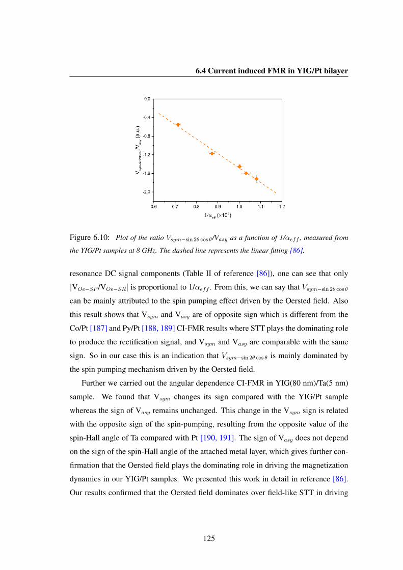
6.4 Current induced FMR in YIG/Pt bilayer
Figure 6.10: Plot of the ratio Vsym−sin 2θ cos θ/Vasy as a function of 1/αeff , measured from
the YIG/Pt samples at 8 GHz. The dashed line represents the linear fitting [86].
resonance DC signal components (Table II of reference [86]), one can see that only
|VOe−SP /VOe−SR| is proportional to 1/αeff . From this, we can say that Vsym−sin 2θ cos θ
can be mainly attributed to the spin pumping effect driven by the Oersted field. Also
this result shows that Vsym and Vasy are of opposite sign which is different from the
Co/Pt [187] and Py/Pt [188, 189] CI-FMR results where STT plays the dominating role
to produce the rectification signal, and Vsym and Vasy are comparable with the same
sign. So in our case this is an indication that Vsym−sin 2θ cos θ is mainly dominated by
the spin pumping mechanism driven by the Oersted field.
Further we carried out the angular dependence CI-FMR in YIG(80 nm)/Ta(5 nm)
sample. We found that Vsym changes its sign compared with the YIG/Pt sample
whereas the sign of Vasy remains unchanged. This change in the Vsym sign is related
with the opposite sign of the spin-pumping, resulting from the opposite value of the
spin-Hall angle of Ta compared with Pt [190, 191]. The sign of Vasy does not depend
on the sign of the spin-Hall angle of the attached metal layer, which gives further con-
firmation that the Oersted field plays the dominating role in driving the magnetization
dynamics in our YIG/Pt samples. We presented this work in detail in reference [86].
Our results confirmed that the Oersted field dominates over field-like STT in driving
125
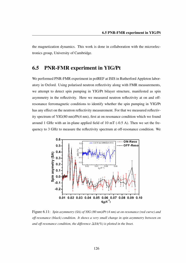
6.5 PNR-FMR experiment in YIG/Pt
the magnetization dynamics. This work is done in collaboration with the microelec-
tronics group, University of Cambridge.
6.5 PNR-FMR experiment in YIG/Pt
We performed PNR-FMR experiment in polREF at ISIS in Rutherford Appleton labor-
atory in Oxford. Using polarised neutron reflectivity along with FMR measurements,
we attempt to detect spin pumping in YIG/Pt bilayer structure, manifested as spin
asymmetry in the reflectivity. Here we measured neutron reflectivity at on and off-
resonance ferromagnetic conditions to identify whether the spin pumping in YIG/Pt
has any effect on the neutron reflectivity measurement. For that we measured reflectiv-
ity spectrum of YIG(80 nm)/Pt(4 nm), first at on resonance condition which we found
around 1 GHz with an in-plane applied field of 10 mT (-0.5 A). Then we set the fre-
quency to 3 GHz to measure the reflectivity spectrum at off-resonance condition. We
Figure 6.11: Spin asymmetry (SA) of YIG (80 nm)/Pt (4 nm) at on-resonance (red curve) and
off-resonance (black) condition. It shows a very small change in spin asymmetry between on
and off-resonance condition, the difference ∆SA(%) is plotted in the Inset.
126

6.5 PNR-FMR experiment in YIG/Pt
Figure 6.12: Simulation of spin asymmetry in YIG (80 nm)/Pt (4nm) bilayer system using
Gen-X. This shows that to detect any change of statistical significance in the spin asymmetry,
moment induced in the Pt should be greater than 0.05 µB/atom. The minimum SA resolution
for the instrument is 0.01 µB/atom.
focussed on small wave vector range qz(A−1). The experimental data were modelled
and analysed by using Gen-X software.
Figure 6.11 shows the spin asymmetry data obtained at on-resonance (red curve)
and off-resonance (black curve) condition. Oscillations are observed within small qz
range, 0.04 A−1. The difference in spin asymmetry, ∆SA(%), is shown in the inset of
figure 6.11. We found no significant change in the spin asymmetry. Next, we carried
out the simulation using Gen-X (figure 6.12) for this bilayer structure to estimate the
amount of spin pumping required to get a noticeable change in spin asymmetry. This
establishes an upper boundary for the change in magnetisation of 0.05 µB/atom, as
seen in our simulation of the SA. The moment induced in the Pt layer is less than 0.05
µB/atom, so it was very hard to detect any change of statistical significance in the spin
asymmetry between on and off-resonance condition.
127
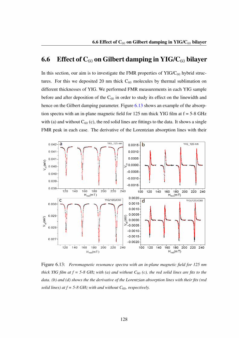
6.6 Effect of C60 on Gilbert damping in YIG/C60 bilayer
6.6 Effect of C60 on Gilbert damping in YIG/C60 bilayer
In this section, our aim is to investigate the FMR properties of YIG/C60 hybrid struc-
tures. For this we deposited 20 nm thick C60 molecules by thermal sublimation on
different thicknesses of YIG. We performed FMR measurements in each YIG sample
before and after deposition of the C60 in order to study its effect on the linewidth and
hence on the Gilbert damping parameter. Figure 6.13 shows an example of the absorp-
tion spectra with an in-plane magnetic field for 125 nm thick YIG film at f = 5-8 GHz
with (a) and without C60 (c), the red solid lines are fittings to the data. It shows a single
FMR peak in each case. The derivative of the Lorentzian absorption lines with their
Figure 6.13: Ferromagnetic resonance spectra with an in-plane magnetic field for 125 nm
thick YIG film at f = 5-8 GHz with (a) and without C60 (c), the red solid lines are fits to the
data. (b) and (d) shows the the derivative of the Lorentzian absorption lines with their fits (red
solid lines) at f = 5-8 GHz with and without C60, respectively.
128

6.6 Effect of C60 on Gilbert damping in YIG/C60 bilayer
Figure 6.14: FMR linewidth as a function of frequency for 125 nm thick YIG with (a) and
without C60 (c), the blue solid lines are fit to the data. From the slope we extracted the damping
parameter in each case, which shows that the damping decreases with C60. (e) FMR linewidth
as a function of frequency for the same sample measured after removing the C60 by using the
acetone, and the damping parameter goes back to the previous value of bare YIG. In (b,d,f) we
plotted the frequency dependence of resonance field with its Kittel fit (red line) which gives the
gyromagnetic ratio 27.7 GHz/T. The effective magnetization does not change with C60.
129
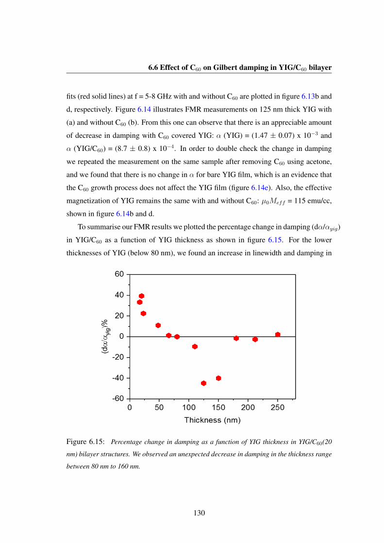
6.6 Effect of C60 on Gilbert damping in YIG/C60 bilayer
fits (red solid lines) at f = 5-8 GHz with and without C60 are plotted in figure 6.13b and
d, respectively. Figure 6.14 illustrates FMR measurements on 125 nm thick YIG with
(a) and without C60 (b). From this one can observe that there is an appreciable amount
of decrease in damping with C60 covered YIG: α (YIG) = (1.47 ± 0.07) x 10−3 and
α (YIG/C60) = (8.7 ± 0.8) x 10−4. In order to double check the change in damping
we repeated the measurement on the same sample after removing C60 using acetone,
and we found that there is no change in α for bare YIG film, which is an evidence that
the C60 growth process does not affect the YIG film (figure 6.14e). Also, the effective
magnetization of YIG remains the same with and without C60: µ0Meff = 115 emu/cc,
shown in figure 6.14b and d.
To summarise our FMR results we plotted the percentage change in damping (dα/αyig)
in YIG/C60 as a function of YIG thickness as shown in figure 6.15. For the lower
thicknesses of YIG (below 80 nm), we found an increase in linewidth and damping in
Figure 6.15: Percentage change in damping as a function of YIG thickness in YIG/C60(20
nm) bilayer structures. We observed an unexpected decrease in damping in the thickness range
between 80 nm to 160 nm.
130

6.6 Effect of C60 on Gilbert damping in YIG/C60 bilayer
YIG/C60 which gives an indication of spin pumping from YIG into C60 molecules. For
very thick films, above 180 nm, we hardly observed any change in damping. This is
because for very thick films the interface become quite rough, so probability of spin
injection into the C60 almost disappears. But we found the result is interesting in the
thickness range between 80 nm to 160 nm, where we noticed an unexpected decrease
in damping, more pronounced in the case of a 125 nm thick film. This is something
which may signify a phenomenon which is reverse of spin pumping effect.
In figure 6.16 we plotted separately the thickness dependence of Gilbert damping
of bare YIG samples which were used for this YIG/C60 experiment. We observed that
damping is not following a definite trend with thickness. This might be due to the
presence of multiple peaks which we cannot distinguish in our Lorentzian absorption
profile. In reference [62], more than one peak has also been reported for a 20 nm thick
film as shown in figure 6.17a. Here they mentioned the additional peaks correspond
to standing spin wave modes which are visible due to the extremely low damping in
the layers. Also, all our samples were not grown in the same growth run, this may be
Figure 6.16: Gilbert damping as a function of YIG thickness. We observed that damping is
not following any definite trend with thickness. This might be due to the presence of mulitple
peaks which we can not distinguish in our Lorentzian spectra. Also all these samples were not
grown in the same growth run.
131
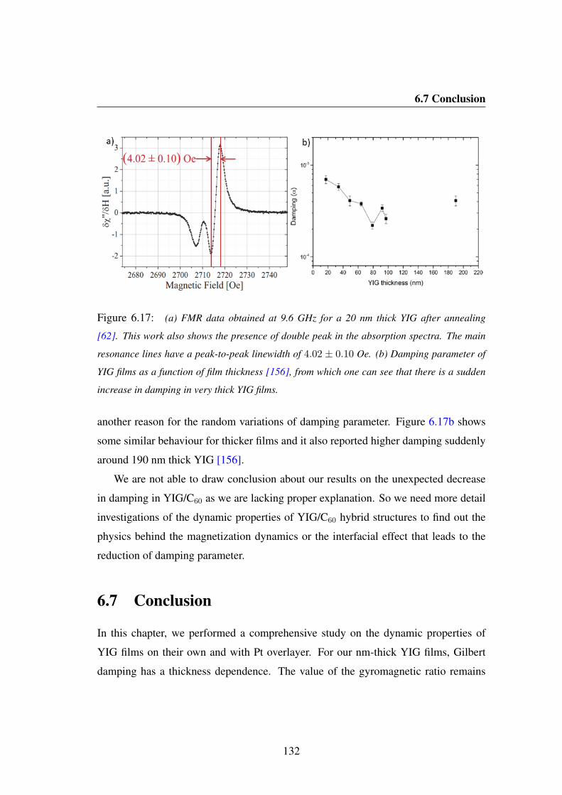
6.7 Conclusion
Figure 6.17: (a) FMR data obtained at 9.6 GHz for a 20 nm thick YIG after annealing
[62]. This work also shows the presence of double peak in the absorption spectra. The main
resonance lines have a peak-to-peak linewidth of 4.02 ± 0.10 Oe. (b) Damping parameter of
YIG films as a function of film thickness [156], from which one can see that there is a sudden
increase in damping in very thick YIG films.
another reason for the random variations of damping parameter. Figure 6.17b shows
some similar behaviour for thicker films and it also reported higher damping suddenly
around 190 nm thick YIG [156].
We are not able to draw conclusion about our results on the unexpected decrease
in damping in YIG/C60 as we are lacking proper explanation. So we need more detail
investigations of the dynamic properties of YIG/C60 hybrid structures to find out the
physics behind the magnetization dynamics or the interfacial effect that leads to the
reduction of damping parameter.
6.7 Conclusion
In this chapter, we performed a comprehensive study on the dynamic properties of
YIG films on their own and with Pt overlayer. For our nm-thick YIG films, Gilbert
damping has a thickness dependence. The value of the gyromagnetic ratio remains
132

6.7 Conclusion
nearly constant and is close to the theoretical value. The FMR profile has a narrow
linewidth of several Oersteds. FMR measurements on our smooth films shows linear
increase of linewidth with frequency, indicating the absence of two-magnon scattering.
Samples made from the Target-A ( 2.6 ± 0.3 x 10⁻⁴ for 38 nm [174]) showed lower
damping compared to the samples deposited from the Target-B ( 1.92 ± 0.1 x 10⁻³
for 38 nm). This indicates a possibility of having inhomogeneties which may result in
non-uniformity in magnetization over a long range or may be due to some deficit in
the right stoichiometry. This work also demonstrates the temperature dependence of
Gilbert damping factor in nm-thick YIG film in the temperature range 20 K to 300 K
which decays exponentially with increase in temperature. We observed a downturn in
effective magnetization at low temperatures. A large value of spin mixing conductance,
(1.6 ± 0.3) x 1019 m−2 for YIG/Pt sample is an indication of a good interface which is
necessary for efficient spin transfer. In continuation of this work, we should investigate
the temperature dependence of damping in YIG on YAG substrate for future studies.
From PNR-FMR results, we get an idea on the amount of moment required to de-
tect significant spin pumping in terms of spin asymmetry in YIG/Pt bilayer structure.
We carried out CI-FMR measurements in a series of YIG/HM samples with different
YIG thickness between 14.8 nm and 80 nm to quantify the current-induce torque. Our
conclusion is, the Oersted field dominates over STT in driving the magnetisation pre-
cession and should therefore be taken into account for CI-FMR studies in YIG/HM
systems. In future, we need to figure out the ways to improve the YIG/metal interface
so that we can realize spin-transfer torque in this system and hence STT devices using
YIG. At last, we investigated the effect of C60 on the damping parameter in YIG/C60
hybrid structures which has not been studied before. For thin samples, we observed
that the damping increases with C60, which is an encouraging result. For certain range
of thicknesses (thicker films), we noticed an unexpected decrease in the damping for
C60 covered YIG samples. This is quite interesting but we are not yet able to predict
the actual physics to explain the magnetization dynamics in this structure. For this we
need further investigations which is currently in progress in our group.
133

CHAPTER 7
Conclusion
134

7.1 Summary
7.1 Summary
This research demonstrates the growth of high quality nanometre thick YIG films by
on-axis RF magnetron sputtering, which are reproducible and consistently exhibit the
required properties of YIG. The results of structural, magnetic and FMR measure-
ments demonstrated a good matching with the ones grown by pulse laser deposition
(PLD), on and off-axis sputtering. These nanometre thick YIG films can be used for
a wider range of research which includes spin pumping, spin transfer torque, spin hall
magnetoresistance (SHMR) and the magnonics community.
A comprehensive study of the crystallinity and morphology of the YIG films shows
a (111) crystalline orientation with RMS surface roughness of about 1-3 A. The lattice
constant of the YIG is close to the bulk value (12.376 A). In collaboration with the Su-
perSTEM Laboratory in Daresbury, we analysed the chemical nature of the YIG/GGG
interface using atomic resolution STEM, indicating an interdiffusion at the YIG/GGG
interface, with 4 - 6 nm Gd-doped region in which Y and Gd diffuse in pairs. A good
fitting (GOF = 0.04) of x-ray reflectivity curve of annealed YIG sample is obtained by
introducing a Gd-mixed YIG layer at the interface. The XRR data fitting returns the
densities for the YIG and GGG which are within 1% of the bulk values. The formation
of interdiffusion layer takes place during the high temperature annealing (850C). The
good agreement between the x-ray data fitting and STEM results allowed us to propose
a two layer model to represent the YIG sample: a Gd-rich YIG layer with a highly dis-
ordered structure near the interface and the upper layer is almost a perfect YIG. This
Gd-mixed YIG interlayer influences the magnetic properties and may also contribute
to the FMR linewidth broadening in YIG, particularly at low temperatures.
The magnetic properties of YIG on (111) oriented GGG substrate are studied ex-
tensively using magnetometry and polarised neutron reflectivity. Due to the paramag-
netism induced by the Gd3+ ions from the GGG and increased saturation field at room
temperature, measurement of the magnetic moment of YIG at low temperatures is
challenging. The YIG films have very low coercivity 0.30 ± 0.05 Oe and a saturation
magnetisation 144 emu/cc at 295 K. Our result on the thickness dependence of the
135

7.1 Summary
saturation magnetic moment confirms the existence of 6 nm dead layer at the interface.
The temperature dependent magnetisation data M(T) reveals the magnetisation sup-
pression at low temperature, below ∼100 K. The temperature dependent PNR results
of 80 nm and 10 nm thick YIG shows an excellent agreement with their M(T) results,
obtained by magnetometry. For 10 nm YIG, the compensation temperature is 100 K
(corresponds to 40% Gd-diffusion) where the magnetization reaches minimum. At low
temperature, Gd spins dominate the magnetic behaviour with its ordering temperature
around 65-85 K and will align antiparallel to the net magnetic moment of YIG. Hence,
the role of Gd-diffused layer in the reduction of magnetisation in YIG films is clearly
understood. The proposed two-layer model fits all the M(T) data consistently for dif-
ferent thicknesses of YIG with a 6 nm thick Gd-diffused YIG layer at the interface.
In phenomena that requires thin YIG films, the magnetic behaviour of the Gd-layer,
which will be paramagnetic at room temperature and gradually align antiparallel as the
sample is cooled, will have to be considered. The M(T) data of YIG on YAG shows
no downturn of magnetisation at low temperatures. This again supports the influence
of Gd-diffusion from GGG on the magnetisation of YIG. The magnetic properties of
YIG on YAG showed low saturation magnetisation (98 emu/cc for 40 nm YIG) and
high coercivity (70 Oe). This is possibly due to the large lattice mismatch between
YIG and YAG.
For our nm-thick YIG films, the FMR profile has a narrow linewidth with extremely
small damping (eg. (2.6± 0.3) x 10−4 for 38 nm YIG). The value of the gyromagnetic
ratio, 27.7 GHz/T is close to the theoretical value. The Gilbert damping parameter
shows a thickness dependence, such that it is inversely proportional to the thickness of
YIG. This work demonstrates the temperature dependence of Gilbert damping factor
in YIG nano films in the temperature range 20 K to 300 K, decaying exponentially
with increase in temperature. It could be possible that the Gd-layer and slow relaxa-
tion mechanisms of rare-earth impurities affecting the magnetization dynamics of pure
YIG, which results in low temperature increase in the FMR linewidth. A large value
of the spin mixing conductance 1.6 x 10¹⁹ m−2 is found in YIG/Pt sample, indicating
136

7.2 Future work
a good interface necessary for efficient spin injection in YIG-based heterostructures.
With PNR-FMR experiments, we get an idea of the amount of moment required to de-
tect significant spin pumping in terms of spin asymmetry in the YIG/Pt bilayer struc-
tures. The FMR results of YIG/C60 hybrid structures shows spin pumping but with rich
underlying physics in the dissipation and uniformity of the FMR signal, which is an
encouraging result for future study. Our collaborative work on the spin wave propaga-
tion in nm-thick YIG films [174] with the University of Regensburg made an important
contribution to the YIG community. We are able to observe spin wave (SW) excitations
at distances up to 150 µm away from the exciting CPW. The spin wave decay length is
about 2.7 µm and 3.6 µm for the 38 nm and 49 nm thick YIG films, respectively. The
CI-FMR measurements in collaboration with the University of Cambridge, shows that
the Oersted field dominates over the spin transfer torque in driving the magnetization
dynamics in YIG/metal bilayer structures [86]. Our research on YIG using the FMR
technique covered a broad area which is important to study the spin pumping and STT
effect in YIG/Pt and other YIG based multilayer structures.
In conclusion, this work demonstrates the growth and complete study of the proper-
ties of epitaxial nm-thick sputtered YIG. We have revealed the nature of this promising
material to the spintronics community. This work discovered the interfacial diffusion
and its effect on the magnetisation of thin YIG. The demand for thin YIG films is
set to increase as the field of magnonics and insulator-based spintronics develops. In
particular, the prospect of being able to use high-quality sputtered YIG, which is the in-
dustrial method for deposition makes YIG films an excellent choice for the spintronics
community.
7.2 Future work
The research work covered in this thesis paves the way for the growth optimization
and more advanced experiments with RF sputtered YIG films and YIG-based bilayer
structures. This section is devoted to the possible future experiments using these films.
137
7.2 Future work
For future studies, it would be good to examine the stoichiometry of the annealed
YIG of different thicknesses. This could be done by X-ray photoelectron spectroscopy
(XPS). For chemical analysis of the top surface of YIG, we can use AFM [192]. The
in-situ annealing can be done to improve the sample quality. The deposition can also be
done with a high substrate temperature that may produce as-deposited epitaxial films.
Piranha etching is the uncontrolled part of YIG surface processing. Alternative clean-
ing steps such as plasma oxidation and ion milling should be consider to get better
interface quality. We identified a 4-6 nm interdiffusion region at the YIG/GGG inter-
face. It can be possible to limit the diffusion by lowering the annealing temperature
and increasing the annealing time to crystallise the structure. There is the possibility
of further improving the quality of the films by optimising the annealing temperat-
ure or using annealed GGG for the growth or introducing a diffusion barrier between
YIG and GGG. We must consider the deposition of YIG films by off-axis sputtering in
varying substrates (GGG and YAG) in the future. We performed intensive research on
the magnetic properties of YIG using magnetometry. In the future, microanalysis of
magnetic structure using magnetic force microscopy (MFM) should be done to get de-
tail information about the inhomogeneous distribution of magnetization of the sample,
which may be related to the multiple peaks observed in FMR results.
Within the scope of this thesis, the first step towards the utilization of sputtered
nm-thick YIG films in spin pumping and current induced FMR have been made. Fol-
lowing our results on the temperature dependence of the Gilbert damping, we should
measure the temperature dependent FMR properties for YIG deposited on YAG. We
are currently undertaking this work in collaboration with the University of Regensburg.
A comparison of α(T) for YIG on GGG and YAG substrate will give us a better un-
derstanding of the physics and the parameters that are dominating at low temperatures.
From this we can also develop an idea about the behaviour of the spin mixing con-
ductance and the propagation/injection of spin currents as a function of temperature.
We should consider surface cleaning of YIG by plasma etching before Pt deposition to
improve the YIG-Pt interface. This will increase the spin pumping efficiency and pos-
138

7.2 Future work
sibility of realising the spin transfer torque in nanoscale YIG. The results obtained from
YIG/C60 structures open a new area to work with molecules on YIG, which can lead to
an exciting research area in the field of molecular spintronics. For better understand-
ing of the effect of C60 on the damping parameter of YIG, we must perform the FMR
measurements of YIG/C60 bilayers films by varying the thickness of the C60 layer. It
will be also interesting to investigate the spin pumping effect in YIG/C60/Pt trilayer
structures by varying the thickness of C60. This work is in progress in our group. Par-
allely, our YIG samples for spin injection experiments in YIG/PBTTT bilayers has also
showed promising results, which give a further opportunity to try different materials
on YIG for spin injection experiments. This work is now in progress in collaboration
with the Optoelectronics group in University of Cambridge. Another aspect of future
work could be the optical spin pumping in YIG/molecular structure. We should also
think about the microfabrication of YIG as it already proved to be a potential material
for insulator based spintronics devices.
139

REFERENCES
[1] N. Mott and B. N. F. Mott, “The electrical conductivity of transition metals,”
Proceedings of the Royal Society of London. Series A, . . . , vol. 153, no. 880,
pp. 699–717, 1936.
[2] N. Mott, F.R.S., and H. Wills, “The Resistance and Thermoelectric Properties of
the Transition Metals,” Proceedings of the Royal Society of London A, vol. 156,
no. 188, pp. 368–382, 1936.
[3] M. N. Baibich, J. M. Broto, A. Fert, F. N. Van Dau, F. Petroff, P. Eitenne,
G. Creuzet, A. Friederich, and J. Chazelas, “Giant magnetoresistance of
(001)Fe/(001)Cr magnetic superlattices,” Physical Review Letters, vol. 61,
no. 21, pp. 2472–2475, 1988.
[4] G. Binasch, P. Grunberg, F. Saurenbach, and W. Zinn, “Enhanced magnetores-
istance in layered magnetic structures with antiferromagnetic interlayer ex-
change,” Physical Review B, vol. 39, no. 7, pp. 4828–4830, 1989.
[5] U. Hartmann, ed., Magnetic Multilayers and Giant Magnetoresistance, vol. 37.
Springer-Verlag Berlin Heidelberg, 2000.
[6] H. S. E. Hirota and K. Inomata, eds., Giant Magneto-Resistance Devices,
vol. 40. Springer-Verlag Berlin Heidelberg, 2002.
[7] J. Daughton, J. Brown, E. Chen, R. Beech, A. Pohm, and W. Kude, “Magnetic
140

REFERENCES
field sensors using GMR multilayer,” Magnetics, IEEE Transactions on, vol. 30,
no. 6, pp. 4608–4610, 1994.
[8] G. A. Prinz, “Magnetoelectronics,” Science, vol. 282, no. November, pp. 1660–
1663, 1998.
[9] M. Julliere, “Tunneling between ferromagnetic films,” Physics Letters A,
vol. 54, no. 3, pp. 225–226, 1975.
[10] T. Miyazaki and N. Tezuka, “Giant magnetic tunneling effect in Fe/Al2O3/Fe
junction,” Journal of Magnetism and Magnetic Materials, vol. 139, no. 3,
pp. 94–97, 1995.
[11] J. Slonczewski, “Current-driven excitation of magnetic multilayers,” Journal of
Magnetism and Magnetic Materials, vol. 159, no. 1-2, pp. L1–L7, 1996.
[12] L. Berger, “Emission of spin waves by a magnetic multilayer traversed by a
current,” PhysRevB, vol. 54, no. 13, pp. 9353–9358, 1996.
[13] J. M. Slaughter, R. W. Dave, M. Deherrera, M. Durlam, B. N. Engel, J. Janesky,
N. D. Rizzo, and S. Tehrani, “Fundamentals of MRAM technology,” Journal of
Superconductivity, vol. 15, no. 1, pp. 19–25, 2002.
[14] T. M. Maffitt, J. K. DeBrosse, J. a. Gabric, E. T. Gow, M. C. Lamorey, J. S.
Parenteau, D. R. Willmott, M. A. Wood, and W. J. Gallagher, “Design consider-
ations for MRAM,” IBM Journal of Research and Development, vol. 50, no. 1,
pp. 25–39, 2006.
[15] J. Katine, F. Albert, R. Buhrman, E. Myers, and D. Ralph, “Current-Driven
Magnetization Reversal and Spin-Wave Excitations in Co /Cu /Co Pillars,”
Physical Review Letters, vol. 84, no. 14, pp. 3149–3152, 2000.
[16] S. S. P. Parkin, M. Hayashi, and L. Thomas, “Magnetic Domain-Wall Racetrack
Memory,” Science, vol. 320, no. 5873, pp. 190–194, 2008.
141
REFERENCES
[17] S. Datta and B. Das, “Electronic analog of the electro-optic modulator,” Applied
Physics Letters, vol. 56, no. 7, pp. 665–667, 1990.
[18] H. C. Koo, J. H. Kwon, J. Eom, J. Chang, S. H. Han, and M. Johnson, “Control
of Spin Precession in a Spin-Injected Field Effect Transistor,” Science, vol. 325,
no. 5947, pp. 1515–1518, 2009.
[19] C. Betthausen, T. Dollinger, H. Saarikoski, V. Kolkovsky, G. Karczewski,
T. Wojtowicz, K. Richter, and D. Weiss, “Spin-Transistor Action via Tunable
Landau-Zener Transitions,” Science, vol. 337, no. 6092, pp. 324–327, 2012.
[20] M. P. Kostylev, A. A. Serga, T. Schneider, B. Leven, and B. Hillebrands, “Spin-
wave logical gates,” Applied Physics Letters, vol. 87, no. 15, pp. 1–3, 2005.
[21] A. A. Serga, A. V. Chumak, and B. Hillebrands, “YIG magnonics,” J. Phys. D:
Appl. Phys., vol. 43, no. 43, pp. 264002–264002, 2010.
[22] V. V. Kruglyak, S. O. Demokritov, and D. Grundler, “Magnonics,” Journal of
Physics D: Applied Physics, vol. 43, no. 26, p. 264001, 2010.
[23] T. Schneider, A. A. Serga, B. Leven, B. Hillebrands, R. L. Stamps, and M. P. Ko-
stylev, “Realization of spin-wave logic gates,” Applied Physics Letters, vol. 92,
no. 2, 2008.
[24] A. Khitun, M. Bao, and K. L. Wang, “Magnonic logic circuits,” Journal of Phys-
ics D: Applied Physics, vol. 43, no. 26, p. 264005, 2010.
[25] B. Lenk, H. Ulrichs, F. Garbs, and M. Munzenberg, “The building blocks of
magnonics,” Physics Reports, vol. 507, no. 4-5, pp. 107–136, 2011.
[26] T. Bracher, F. Heussner, P. Pirro, T. Fischer, M. Geilen, B. Heinz, B. Lagel,
A. A. Serga, and B. Hillebrands, “Time- and power-dependent operation of a
parametric spin-wave amplifier,” Applied Physics Letters, vol. 105, no. 23, 2014.
142

REFERENCES
[27] V. E. Demidov, S. Urazhdin, and S. O. Demokritov, “Direct observation and
mapping of spin waves emitted by spin-torque nano-oscillators.,” Nature mater-
ials, vol. 9, no. 12, pp. 984–988, 2010.
[28] M. Madami, S. Bonetti, G. Consolo, S. Tacchi, G. Carlotti, G. Gubbiotti, F. B.
Mancoff, M. a. Yar, and J. Akerman, “Direct observation of a propagating spin
wave induced by spin-transfer torque,” Nature Nanotechnology, vol. 6, no. 10,
pp. 635–638, 2011.
[29] V. E. Demidov, S. Urazhdin, H. Ulrichs, V. Tiberkevich, A. Slavin, D. Baither,
G. Schmitz, and S. O. Demokritov, “Magnetic nano-oscillator driven by pure
spin current,” Nature Materials, vol. 11, no. 12, pp. 1028–1031, 2012.
[30] Y. Tserkovnyak, A. Brataas, and G. E. W. Bauer, “Enhanced gilbert damping in
thin ferromagnetic films.,” Physical review letters, vol. 88, no. 11, p. 117601,
2002.
[31] M. V. Costache, M. Sladkov, S. M. Watts, C. H. Van Der Wal, and B. J. Van
Wees, “Electrical detection of spin pumping due to the precessing magnetization
of a single ferromagnet,” Physical Review Letters, vol. 97, no. 21, pp. 1–4, 2006.
[32] J. E. Hirsch, “Spin Hall Effect,” Physical Review Letters, vol. 83, no. 9,
pp. 1834–1837, 1999.
[33] E. Saitoh, M. Ueda, H. Miyajima, and G. Tatara, “Conversion of spin cur-
rent into charge current at room temperature: Inverse spin-Hall effect,” Applied
Physics Letters, vol. 88, no. 18, pp. 1–4, 2006.
[34] S. Zhang, “Spin Hall effect in the presence of spin diffusion,” Physical Review
Letters, vol. 85, no. 2, pp. 393–396, 2000.
[35] Y. Kajiwara, K. Harii, S. Takahashi, J. Ohe, K. Uchida, M. Mizuguchi,
H. Umezawa, H. Kawai, K. Ando, K. Takanashi, S. Maekawa, and E. Saitoh,
143

REFERENCES
“Transmission of electrical signals by spin-wave interconversion in a magnetic
insulator.,” Nature, vol. 464, no. 7286, pp. 262–266, 2010.
[36] J. C. Slonczewski, “Initiation of spin-transfer torque by thermal transport from
magnons,” Physical Review B - Condensed Matter and Materials Physics,
vol. 82, no. 5, pp. 1–11, 2010.
[37] K. Uchida, S. Takahashi, K. Harii, J. Ieda, W. Koshibae, K. Ando, S. Maekawa,
and E. Saitoh, “Observation of the spin Seebeck effect.,” Nature, vol. 455,
no. 7214, pp. 778–81, 2008.
[38] K. Uchida, J. Xiao, H. Adachi, J. Ohe, S. Takahashi, J. Ieda, T. Ota, Y. Kajiwara,
H. Umezawa, H. Kawai, G. E. W. Bauer, S. Maekawa, and E. Saitoh, “Spin
Seebeck insulator,” Nature Materials, vol. 9, no. 11, pp. 894–897, 2010.
[39] G. A. M. Alexander G. Gurevich, Magnetization Oscillations and Waves. CRC
Press, 1996.
[40] K. ichi Uchida, T. Kikkawa, A. Miura, J. Shiomi, and E. Saitoh, “Quantitative
temperature dependence of longitudinal spin seebeck effect at high temperat-
ures,” Physical Review X, vol. 4, no. 4, pp. 1–9, 2014.
[41] X. Jia, K. Liu, K. Xia, and G. E. W. Bauer, “Spin transfer torque on magnetic
insulators,” EPL (Europhysics Letters), vol. 96, no. 1, p. 4, 2011.
[42] C. Du, H. Wang, F. Yang, and P. C. Hammel, “Systematic variation of spin-orbit
coupling with d -orbital filling: Large inverse spin Hall effect in 3d transition
metals,” Physical Review B - Condensed Matter and Materials Physics, vol. 90,
no. 14, pp. 1–5, 2014.
[43] H. Jin, S. R. Boona, Z. Yang, R. C. Myers, and J. P. Heremans, “Effect of
the magnon dispersion on the longitudinal spin Seebeck effect in yttrium iron
garnets,” Physical Review B - Condensed Matter and Materials Physics, vol. 92,
no. 5, 2015.
144
REFERENCES
[44] D. J. Sanders and D. Walton, “Effect of magnon-phonon thermal relaxation on
heat transport by magnons,” Physical Review B, vol. 15, no. 3, pp. 1489–1494,
1977.
[45] T. Kikkawa, K. I. Uchida, S. Daimon, Z. Qiu, Y. Shiomi, and E. Saitoh, “Critical
suppression of spin Seebeck effect by magnetic fields,” Physical Review B -
Condensed Matter and Materials Physics, vol. 92, no. 6, pp. 1–9, 2015.
[46] H. L. Wang, C. H. Du, Y. Pu, R. Adur, P. C. Hammel, and F. Y. Yang, “Scaling
of spin hall angle in 3d, 4d, and 5d metals from Y3Fe5O12 /metal spin pumping,”
Physical Review Letters, vol. 112, no. 19, pp. 1–5, 2014.
[47] C. H. Du, H. L. Wang, Y. Pu, T. L. Meyer, P. M. Woodward, F. Y. Yang, and P. C.
Hammel, “Probing the spin pumping mechanism: Exchange coupling with ex-
ponential decay in Y3Fe5O12/barrier/Pt heterostructures,” Physical Review Let-
ters, vol. 111, no. 24, pp. 1–5, 2013.
[48] C. Du, H. Wang, F. Yang, and P. C. Hammel, “Enhancement of Pure Spin Cur-
rents in Spin Pumping Y3Fe5O12/Cu/Metal Trilayers through Spin Conductance
Matching,” Physical Review Applied, vol. 1, no. 4, 2014.
[49] H. Wang, C. Du, P. Chris Hammel, and F. Yang, “Spin current and inverse spin
Hall effect in ferromagnetic metals probed by Y3Fe5O12-based spin pumping,”
Applied Physics Letters, vol. 104, no. 20, 2014.
[50] T. Chiba, G. E. W. Bauer, and S. Takahashi, “Spin torque transistor revisited,”
Applied Physics Letters, vol. 102, no. 19, 2013.
[51] M. B. Jungfleisch, V. Lauer, R. Neb, a. V. Chumak, and B. Hillebrands, “Im-
provement of the yttrium iron garnet/platinum interface for spin pumping-based
applications,” Applied Physics Letters, vol. 103, no. 2, pp. 2011–2015, 2013.
[52] Y. Sun, H. Chang, M. Kabatek, Y. Y. Song, Z. Wang, M. Jantz, W. Schneider,
M. Wu, E. Montoya, B. Kardasz, B. Heinrich, S. G. E. Te Velthuis, H. Schulthe-
145

REFERENCES
iss, and A. Hoffmann, “Damping in yttrium iron garnet nanoscale films capped
by platinum,” Physical Review Letters, vol. 111, no. 10, 2013.
[53] S. M. Rezende, R. L. Rodrıguez-Suarez, M. M. Soares, L. H. Vilela-Leao,
D. Ley Domınguez, and a. Azevedo, “Enhanced spin pumping damping in Yt-
trium Iron Garnet/Pt bilayers,” Applied Physics Letters, vol. 102, no. 1, pp. 1–4,
2013.
[54] Y. Sun, Y. Y. Song, H. Chang, M. Kabatek, M. Jantz, W. Schneider, M. Wu,
H. Schultheiss, and A. Hoffmann, “Growth and ferromagnetic resonance prop-
erties of nanometer-thick yttrium iron garnet films,” Applied Physics Letters,
vol. 101, no. 15, p. 082405, 2012.
[55] N. Kumar, D. S. Misra, N. Venkataramani, S. Prasad, and R. Krishnan, “Mag-
netic properties of pulsed laser ablated YIG thin films on different substrates,”
in Journal of Magnetism and Magnetic Materials, vol. 272-276, 2004.
[56] E. Popova, N. Keller, F. Gendron, M. Guyot, M. C. Brianso, Y. Dumond,
and M. Tessier, “Structure and magnetic properties of yttrium-iron-garnet thin
films prepared by laser deposition,” Journal of Applied Physics, vol. 90, no. 3,
pp. 1422–1428, 2001.
[57] N. S. Sokolov, V. V. Fedorov, A. M. Korovin, S. M. Suturin, D. A. Baranov, S. V.
Gastev, B. B. Krichevtsov, K. Y. Maksimova, A. I. Grunin, V. E. Bursian, L. V.
Lutsev, and M. Tabuchi, “Thin yttrium iron garnet films grown by pulsed laser
deposition: Crystal structure, static, and dynamic magnetic properties,” Journal
of Applied Physics, vol. 119, no. 2, 2016.
[58] M. Haidar, M. Ranjbar, M. Balinsky, R. K. Dumas, S. Khartsev, and J. Akerman,
“Thickness- and temperature-dependent magnetodynamic properties of yttrium
iron garnet thin films,” Journal of Applied Physics, vol. 117, no. 17, 2015.
146
REFERENCES
[59] O. D’Allivy Kelly, A. Anane, R. Bernard, J. Ben Youssef, C. Hahn, A. H.
Molpeceres, C. Carretero, E. Jacquet, C. Deranlot, P. Bortolotti, R. Lebour-
geois, J. C. Mage, G. De Loubens, O. Klein, V. Cros, and A. Fert, “Inverse spin
Hall effect in nanometer-thick yttrium iron garnet/Pt system,” Applied Physics
Letters, vol. 103, no. 8, 2013.
[60] L. V. Lutsev, A. M. Korovin, V. E. Bursian, S. V. Gastev, V. V. Fedorov, S. M. Su-
turin, and N. S. Sokolov, “Low-relaxation spin waves in laser-molecular-beam
epitaxy grown nanosized yttrium iron garnet films,” Applied Physics Letters,
vol. 108, no. 18, 2016.
[61] A. Kaveev, V. Bursian, S. Gastev, B. Krichevtsov, S. Suturin, M. Volkov, and
N. Sokolov, “Laser MBE-grown yttrium iron garnet films on GaN: Character-
ization of the crystal structure and magnetic properties,” Materials Research
Express, vol. 3, no. 7, 2016.
[62] C. Hauser, T. Richter, N. Homonnay, C. Eisenschmidt, H. Deniz, D. Hesse,
S. Ebbinghaus, G. Schmidt, and N. Weinberg, “Yttrium Iron Garnet Thin Films
with Very Low Damping Obtained by Recrystallization of Amorphous Mater-
ial,” arXiv:1502.06724v2, no. February, pp. 1–13, 2016.
[63] T. Liu, H. Chang, V. Vlaminck, Y. Sun, M. Kabatek, A. Hoffmann, L. Deng, and
M. Wu, “Ferromagnetic resonance of sputtered yttrium iron garnet nanometer
films,” Journal of Applied Physics, vol. 115, no. 17, pp. 2014–2017, 2014.
[64] J. Lustikova, Y. Shiomi, Z. Qiu, T. Kikkawa, R. Iguchi, K. Uchida, and
E. Saitoh, “Spin current generation from sputtered Y3Fe5O12 films,” Journal
of Applied Physics, vol. 116, no. 15, p. 153902, 2014.
[65] H. L. Wang, C. H. Du, Y. Pu, R. Adur, P. C. Hammel, and F. Y. Yang, “Large
spin pumping from epitaxial Y3Fe5O12 thin films to Pt and W layers,” Physical
Review B - Condensed Matter and Materials Physics, vol. 88, no. 10, pp. 1–5,
2013.
147
REFERENCES
[66] Y.-M. Kang, S.-H. Wee, S.-I. Baik, S.-G. Min, S.-C. Yu, S.-H. Moon, Y.-W.
Kim, and S.-I. Yoo, “Magnetic properties of YIG (Y3Fe5O12) thin films prepared
by the post annealing of amorphous films deposited by rf-magnetron sputtering,”
Journal of Applied Physics, vol. 97, no. 10, p. 10A319, 2005.
[67] F. Bertaut and F. Forrat, “The structure of the ferrimagnetic rare earth ferrites,”
Compt. rend. (1956), 242, 382-4., 1956.
[68] S. Geller and M. A. Gilleo, “Structure and ferrimagnetism of yttrium and rare-
earth-iron garnets,” Acta Crystallographica, vol. 10, no. 3, p. 239, 1957.
[69] P. E. Wigen, R. D. McMichael, and C. Jayaprakash, “Route to chaos in the mag-
netic garnets,” Journal of Magnetism and Magnetic Materials, vol. 84, no. 3,
pp. 237–246, 1990.
[70] D. D. Stancil and A. Prabhakar, Spin Waves. Springer US, 2009.
[71] M. Sparks, Ferromagnetic-relaxation theory. McGraw-Hill advanced physics
monograph series, McGraw-Hill, 1964.
[72] M. Jungfleisch, “Wellenvektoraufgeloste Brillouin-Lichtstreuspektroskopie an
nichtlinearen Spinwellen,” 2009.
[73] M. A. Gilleo and S. Geller, “Magnetic and Crystallographic Properties of Sub-
stituted Yttrium-Iron Garnet, 3Y2O3.xM2O3.(5-x)Fe2O3,” Physical Review,
vol. 110, no. 1, pp. 73–78, 1958.
[74] Z. Celinski and B. Heinrich, “Ferromagnetic resonance linewidth of Fe ultrathin
films grown on a bcc Cu substrate,” Journal of Applied Physics, vol. 70, no. 10,
pp. 5935–5937, 1991.
[75] L. Landau and E. Lifshits, “On the Theory of the Dispersion of Magnetic Per-
meability in Ferromagnetic Bodies,” Phys. Zeitsch. der Sow., vol. 169, no. 14,
pp. 14–22, 1935.
148
REFERENCES
[76] T. Gilbert, “Classics in Magnetics A Phenomenological Theory of Damping
in Ferromagnetic Materials,” IEEE Transactions on Magnetics, vol. 40, no. 6,
pp. 3443–3449, 2004.
[77] H. Suhl, “Theory of the magnetic damping constant,” IEEE Transactions on
Magnetics, vol. 34, no. 4 PART 1, pp. 1834–1838, 1998.
[78] M. Jungfleisch, Spin pumping and inverse spin Hall effect in yttrium iron garnet/
platinum heterostructures. PhD thesis, Fachbereich Physik, TU Kaiserslautern,
2013.
[79] Griffiths J. H. E., “Anomalous High-frequency Resistance of Ferromagnetic
Metals,” Nature, vol. 158, no. 4019, pp. 670–671, 1946.
[80] C. Kittel, “Interpretation of anomalous larmor frequencies in ferromagnetic res-
onance experiment [5],” Physical Review, vol. 71, no. 4, pp. 270–271, 1947.
[81] C. Kittel, “On the theory of ferromagnetic resonance absorption,” Physical Re-
view, vol. 73, no. 2, pp. 155–161, 1948.
[82] E. B. Myers, D. C. Ralph, J. A. Katine, R. N. Louie, and R. A. Buhrman,
“Current-Induced Switching of Domains in Magnetic Multilayer Devices,” Sci-
ence, vol. 285, no. 5429, pp. 867–870, 1999.
[83] A. Brataas, Y. V. Nazarov, and G. E. W. Bauer, “Finite-Element Theory of Trans-
port in Ferromagnet-Normal Metal Systems,” Physical Review Letters, vol. 84,
no. 11, pp. 2481–2484, 2000.
[84] G. Woltersdorf, SPIN-PUMPING AND TWO-MAGNON SCATTERING IN
MAGNETIC MULTILAYERS. PhD thesis, 2004.
[85] M. B. Jungfleisch, A. V. Chumak, A. Kehlberger, V. Lauer, D. H. Kim, M. C.
Onbasli, C. A. Ross, M. Klaui, and B. Hillebrands, “Thickness and power de-
pendence of the spin-pumping effect in Y3Fe5O12 /Pt heterostructures measured
149
REFERENCES
by the inverse spin Hall effect,” Physical Review B - Condensed Matter and
Materials Physics, vol. 91, no. 13, 2015.
[86] Z. Fang, A. Mitra, A. L. Westerman, M. Ali, C. Ciccarelli, O. Cespedes, B. J.
Hickey, and A. J. Ferguson, “Thickness dependence study of current-driven fer-
romagnetic resonance in Y3Fe5O12/heavy metal bilayers,” Applied Physics Let-
ters, vol. 110, no. 9, 2017.
[87] M. Schreier, T. Chiba, A. Niedermayr, J. Lotze, H. Huebl, S. Geprags, S. Taka-
hashi, G. E. W. Bauer, R. Gross, and S. T. B. Goennenwein, “Current-induced
spin torque resonance of a magnetic insulator,” Physical Review B - Condensed
Matter and Materials Physics, vol. 92, no. 14, pp. 1–6, 2015.
[88] M. B. Jungfleisch, W. Zhang, J. Sklenar, J. Ding, W. Jiang, H. Chang, F. Y.
Fradin, J. E. Pearson, J. B. Ketterson, V. Novosad, M. Wu, and A. Hoffmann,
“Large Spin-Wave Bullet in a Ferrimagnetic Insulator Driven by the Spin Hall
Effect,” Physical Review Letters, vol. 116, no. 5, pp. 1–6, 2016.
[89] J. D. Jackson, Classical Electrodynamics, 3rd Edition. John Wiley & Sons,
1998.
[90] E. S. Katsuaki Sato, ed., Spintronics for Next Generation Innovative Devices.
JohnWiley & Sons Ltd, 2015.
[91] I. Zutic, J. Fabian, and S. D. Sarma, “Spintronics: Fundamentals and applica-
tions,” Reviews of Modern Physics, vol. 76, no. 2, pp. 323–410, 2004.
[92] S. P. Helmut Kronmuller, ed., Handbook of Magnetism and Advanced Magnetic
Materials. Wiley-Blackwell, 2007.
[93] M. I. D’yakonov and V. I. Perel’, “Possibility of orienting electron spins with
current,” JETP Letters, vol. 13, no. 11, pp. 467–469, 1971.
150
REFERENCES
[94] M. I. Dyakonov and V. I. Perel, “Current-induced spin orientation of electrons
in semiconductors,” Physics Letters A, vol. 35, no. 6, pp. 459–460, 1971.
[95] N. P. Stern, S. Ghosh, G. Xiang, M. Zhu, N. Samarth, and D. D. Awschalom,
“Current-induced polarization and the spin hall effect at room temperature,”
Physical Review Letters, vol. 97, no. 12, pp. 1–4, 2006.
[96] Y. K. Kato, R. C. Myers, A. C. Gossard, and D. D. Awschalom, “Observation
of the Spin Hall Effect in Semiconductors,” Science (New York, N.Y.), vol. 306,
no. 2004, pp. 1910–1913, 2004.
[97] J. Wunderlich, B. Kaestner, J. Sinova, and T. Jungwirth, “Experimental obser-
vation of the spin-hall effect in a two-dimensional spin-orbit coupled semicon-
ductor system,” Physical Review Letters, vol. 94, no. 4, pp. 1–4, 2005.
[98] V. Sih, R. C. Myers, Y. K. Kato, W. H. Lau, A. C. Gossard, and D. D. Awscha-
lom, “Spatial imaging of the spin Hall effect and current-induced polarization in
two-dimensional electron gases,” Nature Physics, vol. 1, no. 1, pp. 31–35, 2005.
[99] S. O. Valenzuela and M. Tinkham, “Direct electronic measurement of the spin
Hall effect.,” Nature, vol. 442, no. 7099, pp. 176–9, 2006.
[100] T. Kimura, Y. Otani, T. Sato, S. Takahashi, and S. Maekawa, “Room-
temperature reversible spin hall effect,” Physical Review Letters, vol. 98, no. 15,
pp. 1–4, 2007.
[101] T. Tanaka, H. Kontani, M. Naito, T. Naito, D. S. Hirashima, K. Yamada, and
J. Inoue, “Intrinsic spin Hall effect and orbital Hall effect in 4d and 5d transition
metals,” Physical Review B - Condensed Matter and Materials Physics, vol. 77,
no. 16, pp. 1–16, 2008.
[102] R. Winkler, Spin Orbit Coupling Effects in Two-Dimensional Electron and Hole
Systems. Springer Berlin Heidelberg, 2003.
151

REFERENCES
[103] G. Vignale, “Ten years of spin hall effect,” Journal of Superconductivity and
Novel Magnetism, vol. 23, no. 1, pp. 3–10, 2010.
[104] L. Berger, “Side-jump mechanism for the hall effect of ferromagnets,” Physical
Review B, vol. 2, no. 11, pp. 4559–4566, 1970.
[105] R. Karplus and J. M. Luttinger, “Hall effect in ferromagnetics,” Physical Review,
vol. 95, no. 5, pp. 1154–1160, 1954.
[106] N. Mott and H. Massey, The theory of atomic collisions. International series of
monographs on physics. International series of monographs on physics (Oxford,
England), Oxford; 3rd edition (November 1965), 1965.
[107] L.D.Landau and E.M.Lifshitz, Landau-Lifschitz Quantum-Mechanics Non-
relativistic theory, vol. 3. WILEY-VCH, 1964.
[108] S. K. Lyo and T. Holstein, “Side-Jump Mechanism for Ferromagnetic Hall Ef-
fect,” Physical Review Letters, vol. 29, no. 7, pp. 423–425, 1972.
[109] S. Takahashi and S. Maekawa, “Spin current, spin accumulation and spin Hall
effect,” Science and Technology of Advanced Materials, vol. 9, no. 1, p. 014105,
2008.
[110] K. Ando, S. Takahashi, J. Ieda, Y. Kajiwara, H. Nakayama, T. Yoshino, K. Harii,
Y. Fujikawa, M. Matsuo, S. Maekawa, and E. Saitoh, “Inverse spin-Hall ef-
fect induced by spin pumping in metallic system,” Journal of Applied Physics,
vol. 109, no. 10, 2011.
[111] H. A. Kiyotaka Wasa, Makoto Kitabatake, Thin Film Materials Technology:
Sputtering of Compound Materials. William Andrew, 2004, 2004.
[112] C. J. D. Windover E. Barnat J. Y. Kim M. Nielsen T.M. Lu A. Kumar H. Bakhru
and S. L. Lee, “Thin film density determination by multiple radiation energy
152
REFERENCES
dispersive x-ray reflectivity,” JCPDS-International Centre for Diffraction Data
2000, Advances in X-ray Analysis, vol. 42, pp. 590–600, 2000.
[113] J. Als-Nielsen and D. McMorrow, Elements of Modern X-Ray Physics. John
Wiley and Sons Ltd, 2001.
[114] H. Kiessig, “Untersuchungen zur totalreflexion von rontgenstrahlen,” Annalen
der Physik, vol. 402, no. 6, pp. 715–768, 1931.
[115] U. Pietsch, V. Holy, and T. Baumbach, High-resolution X-Ray scattering: from
thin films to lateral nanostructures. Advanced Texts in Physics, Springer New
York, 2004.
[116] N. Porter, Magnetoresistance in n-type Silicon. PhD thesis, School of Physics
and Astronomy, University of Leeds, September 2010.
[117] G. Aviv, “SQUIDs-Superconducting Quantum Interference Devices,” Experi-
mental physics course, 2008.
[118] C. Graham, “High-sensitivity magnetization measurements,” Journal of Mater-
ials Sciences and Technology, vol. 16, no. 02, pp. 97–101, 2000.
[119] J. Clarke and A. I. Braginski, The SQUID Handbook. Wiley VCH, 2005.
[120] G. Binnig and C. F. Quate, “Atomic Force Microscope,” Physical Review Let-
ters, vol. 56, no. 9, pp. 930–933, 1986.
[121] A. S. Paulo and R. Garcıa, “Unifying theory of tapping-mode atomic-force mi-
croscopy,” Physical Review B, vol. 66, no. 4, p. 041406, 2002.
[122] R. Garcia and R. Perez, “Dynamic atomic force microscopy methods,” Surface
Science Reports, vol. 47, pp. 197–301, 2002.
[123] N. Jalili and K. Laxminarayana, “A review of atomic force microscopy imaging
systems: Application to molecular metrology and biological sciences,” Mechat-
ronics, vol. 14, no. 8, pp. 907–945, 2004.
153
REFERENCES
[124] B. H. J. Anthony C. Bland, ed., Ultrathin Magnetic Structures III. Springer
Berlin Heidelberg, 2005.
[125] S. V.F., NEUTRON OPTICS. An Introduction to the Theory of Neutron Optical
Phenomena and their Applications. Oxford University Press, 1989.
[126] b. H. Fritzsche, Z. Yamani, R. Cowley, R. Ward, and H. Fritzsche, “Polarised
neutron reflectometry as a unique tool in magnetization reversal studies of thin
films and multilayers.,” La Physique Au Canada, 2006.
[127] J. F. Ankner and G. P. Felcher, “Polarized-neutron reflectometry,” Journal of
Magnetism and Magnetic Materials, Volume 200, Issue 1-3, p. 741-754, 1999.
[128] C. Kinane, The interplay of magnetism and structure in patterned multilayer
thin films. PhD thesis, School of Physics and Astronomy, University of Leeds,
2008.
[129] V. G. Gavriljuk, A. Dobrinsky, B. D. Shanina, and S. P. Kolesnik, “A study of
the magnetic resonance in a single-crystal Ni 50.47 Mn 28.17 Ga 21.36 alloy,”
Journal of Physics: Condensed Matter, vol. 18, no. 32, pp. 7613–7627, 2006.
[130] M. Dıaz de Sihues, C. Durante-Rincon, and J. Fermin, “A ferromagnetic res-
onance study of NiFe alloy thin films,” Journal of Magnetism and Magnetic
Materials, vol. 316, no. 2, pp. e462–e465, 2007.
[131] Z. Zhang, L. Zhou, P. E. Wigen, and K. Ounadjela, “Angular dependence of fer-
romagnetic resonance in exchange-coupled Co/Ru/Co trilayer structures,” Phys-
ical Review B, vol. 50, no. 9, pp. 6094–6112, 1994.
[132] B. Heinrich, Y. Tserkovnyak, G. Woltersdorf, A. Brataas, R. Urban, and G. E. W.
Bauer, “Dynamic exchange coupling in magnetic bilayers.,” Physical Review
Letters, vol. 90, no. May, p. 187601, 2003.
154
REFERENCES
[133] V. P. Nascimento, E. Baggio Saitovitch, F. Pelegrini, L. C. Figueiredo,
A. Biondo, and E. C. Passamani, “Ferromagnetic resonance study of the ex-
change bias field in NiFeFeMnNiFe trilayers,” Journal of Applied Physics,
vol. 99, no. 8, pp. 8–10, 2006.
[134] M. Oogane, T. Wakitani, S. Yakata, R. Yilgin, Y. Ando, A. Sakuma, and
T. Miyazaki, “Magnetic damping in ferromagnetic thin films,” Japanese Journal
of Applied Physics, Part 1: Regular Papers and Short Notes and Review Papers,
vol. 45, no. 5 A, pp. 3889–3891, 2006.
[135] R. Urban, G. Woltersdorf, and B. Heinrich, “Gilbert damping in single and mul-
tilayer ultrathin films: role of interfaces in nonlocal spin dynamics.,” Physical
review letters, vol. 87, no. 21, p. 217204, 2001.
[136] R. Komiya, T. Kato, N. Nishizawa, S. Tsunashima, and S. Iwata, “Composi-
tional dependence of g -factor and damping constant of (Gd 100- x RE x )FeCo
alloy films (RE = Yb, Tm, Er),” Journal of Physics: Conference Series, vol. 200,
no. 4, p. 042010, 2010.
[137] National Instruments, “Introduction to Network Analyzer Measurements,” Na-
tional Instruments RF Academy, pp. 1–44, 2012.
[138] D. P. B. Gareth R. Eaton, Sandra S. Eaton and R. T. Weber, Quantitative EPR.
Springer-Verlag Wien, 2010.
[139] J. P. Castera, “State of the art in design and technology of MSW devices (in-
vited),” Journal of Applied Physics, vol. 55, no. 6, pp. 2506–2511, 1984.
[140] A. A. S. A. V. Chumak, V. I. Vasyuchka and B. Hillebrands, “Magnon spintron-
ics,” nature physics, vol. 11, no. June, 2015.
[141] M. Collet, M. Evelt, V. E. Demidov, J. L. Prieto, M. Munoz, and J. B.
Youssef, “Nano-patterned magnonic crystals based on ultrathin YIG films,”
arXiv:1705.02267, pp. 1–13, 2017.
155
REFERENCES
[142] A. V. Chumak, A. a. Serga, and B. Hillebrands, “Magnon transistor for all-
magnon data processing,” Nature Communications, vol. 5, no. May 2013,
p. 4700, 2014.
[143] T. Kikkawa, K. Uchida, Y. Shiomi, Z. Qiu, D. Hou, D. Tian, H. Nakayama, X. F.
Jin, and E. Saitoh, “Longitudinal spin seebeck effect free from the proximity
nernst effect,” Physical Review Letters, vol. 110, no. 6, pp. 1–5, 2013.
[144] C. W. Sandweg, Y. Kajiwara, K. Ando, E. Saitoh, and B. Hillebrands, “Enhance-
ment of the spin pumping efficiency by spin wave mode selection,” Applied
Physics Letters, vol. 97, no. 25, pp. 2012–2015, 2010.
[145] J. Xiao, G. E. W. Bauer, K. C. Uchida, E. Saitoh, and S. Maekawa, “Theory
of magnon-driven spin Seebeck effect,” Physical Review B - Condensed Matter
and Materials Physics, vol. 81, no. 21, pp. 1–8, 2010.
[146] E. Padron-Hernandez, A. Azevedo, and S. M. Rezende, “Amplification of spin
waves by thermal spin-transfer torque,” Physical Review Letters, vol. 107,
no. 19, pp. 1–5, 2011.
[147] H. Kurebayashi, O. Dzyapko, V. E. Demidov, D. Fang, A. J. Ferguson, and
S. O. Demokritov, “Controlled enhancement of spin-current emission by three-
magnon splitting.,” Nature materials, vol. 10, no. 9, pp. 660–4, 2011.
[148] S. A. Manuilov, R. Fors, S. I. Khartsev, and A. M. Grishin, “Submicron
Y3Fe5O12 film magnetostatic wave band pass filters,” Journal of Applied Phys-
ics, vol. 105, no. 3, 2009.
[149] J. C. Gallagher, A. S. Yang, J. T. Brangham, B. D. Esser, S. P. White, M. R.
Page, K. Y. Meng, S. Yu, R. Adur, W. Ruane, S. R. Dunsiger, D. W. McComb,
F. Yang, and P. C. Hammel, “Exceptionally high magnetization of stoichiomet-
ric Y3Fe5O12 epitaxial films grown on Gd3Ga5O12,” Applied Physics Letters,
vol. 109, no. 7, 2016.
156
REFERENCES
[150] M. Paul, “Piranha clean procedure,” pp. 1–3, 2010.
[151] P. Hartel, H. Rose, and C. Dinges, “Conditions and reasons for incoherent ima-
ging in STEM,” Ultramicriscopy, vol. 63, no. 96, pp. 93–114, 1996.
[152] V. V. Pan’Kov and L. A. Bashkirov, “Cationic interdiffusion in some garnets,”
Journal of Solid State Chemistry, vol. 60, no. 1, pp. 123–127, 1985.
[153] D. J. Cherniak, “Rare earth element and gallium diffusion in yttrium aluminum
garnet,” Physics and Chemistry of Minerals, vol. 26, no. 2, pp. 156–163, 1998.
[154] C. Pascual-Izarra, M. A. Reis, and N. P. Barradas, “Simultaneous PIXE and RBS
data analysis using Bayesian inference with the DataFurnace code,” Nuclear
Instruments and Methods in Physics Research, Section B: Beam Interactions
with Materials and Atoms, vol. 249, no. 1-2 SPEC. ISS., pp. 780–783, 2006.
[155] C. Du, H. Wang, P. C. Hammel, and F. Yang, “Y3Fe5O12 spin pumping for
quantitative understanding of pure spin transport and spin Hall effect in a broad
range of materials (invited),” Journal of Applied Physics, vol. 117, no. 17, 2015.
[156] M. C. Onbasli, A. Kehlberger, D. H. Kim, G. Jakob, M. Klaui, A. V. Chumak,
B. Hillebrands, and C. A. Ross, “Pulsed laser deposition of epitaxial yttrium
iron garnet films with low Gilbert damping and bulk-like magnetization,” APL
Materials, vol. 2, no. 10, 2014.
[157] M. Aldosary, J. Li, C. Tang, Y. Xu, J.-g. Zheng, and N. Krassimir, “Platinum
/ Yttrium Iron Garnet Inverted Structures for Spin Current Transport,” Applied
Physics Letters, vol. 108, no. 242401, pp. 1–5, 2016.
[158] T. Yamagishi, J. Awaka, Y. Kawashima, M. Uemura, S. Ebisu, S. Chikazawa,
and S. Nagata, “Ferrimagnetic order in the mixed garnet ( Y1−X GdX),” Philo-
sophical Magazine, vol. 6435, no. July, 2005.
157
REFERENCES
[159] L. Benjamin and K. J. Button, Microwave ferrites and ferrimagnetics. McGraw-
Hill Book Company, 1962.
[160] C. Kittel, Introduction to solid state physics, vol. 8. Wiley New York, 1996.
[161] K. P. Belov, E. V. Talalaeva, and G. A. Yarkho, “Magnetic Properties of Rare-
earth Iron Garnets in the Curie-point Region,” Soviet Journal of Experimental
and Theoretical Physics, vol. 25, no. 6, p. 989, 1967.
[162] S. Geprags, A. Kehlberger, T. Schulz, C. Mix, F. Della Coletta, S. Meyer,
A. Kamra, M. Althammer, G. Jakob, H. Huebl, R. Gross, S. T. B. Goennen-
wein, and M. Klaui, “Origin of the spin Seebeck effect probed by temperature
dependent measurements inGd3Fe5O12,” arXiv:1405.4971, pp. 1–6, 2014.
[163] G. F. Dionne, Magnetic Oxides. Springer US, 2009.
[164] R. Pauthenet, “Spontaneous magnetization of some garnet ferrites and the alu-
minum substituted garnet ferrites,” Journal of Applied Physics, vol. 29, no. 3,
pp. 253–255, 1958.
[165] D. Rodic, Z. Tomkowicz, L. Novakovic, A. Szytula, and M. L. Napijalo, “The
initial magnetic susceptibilities of Gd3Fe5O12 and Tb3Fe5O12 in the compens-
ation point region,” Solid State Communications, vol. 73, no. 3, pp. 243–246,
1990.
[166] G. Vertesy and I. Tomas, “Survey of the dependence on temperature of the co-
ercivity of garnet films,” Journal of Applied Physics, vol. 77, no. 12, pp. 6426–
6431, 1995.
[167] B. Keszei, “Modifying the temperature dependence of magnetic garnet film co-
ercivity by etching,” Journal of Applied Physics, vol. 86, no. 11, 1999.
[168] M. Bjorck and G. Andersson, “GenX: An extensible X-ray reflectivity refine-
ment program utilizing differential evolution,” Journal of Applied Crystallo-
graphy, vol. 40, no. 6, pp. 1174–1178, 2007.
158

REFERENCES
[169] M. R. Fitzsimmons and C. F. Majkzak, Application of polarized neutron reflec-
tometry to studies of artificially structured magnetic materials. Springer US,
2005.
[170] B. Knorr and W. Tolksdorf, “Lattice parameters and misfits of gallium garnets
and iron garnet epitaxial layers at temperatures between 294 and 1300 k,” Ma-
terials Research Bulletin, vol. 19, pp. 1507–1513, 1984.
[171] E. Schlomann, J. J. Green, and U. Milano, “Recent developments in ferromag-
netic resonance at high power levels,” Journal of Applied Physics, vol. 386,
no. 5, 1960.
[172] M. Zwierzycki, Y. Tserkovnyak, P. J. Kelly, A. Brataas, and G. E. W. Bauer,
“First-principles study of magnetization relaxation enhancement and spin trans-
fer in thin magnetic films,” Physical Review B - Condensed Matter and Materi-
als Physics, vol. 71, no. 6, pp. 1–11, 2005.
[173] D. Huertas-Hernando, F. Guinea, and A. Brataas, “Spin-orbit coupling in curved
graphene, fullerenes, nanotubes, and nanotube caps,” Physical Review B - Con-
densed Matter and Materials Physics, vol. 74, no. 15, 2006.
[174] A. Talalaevskij, M. Decker, J. Stigloher, A. Mitra, H. S. Korner, O. Cespedes,
C. H. Back, and B. J. Hickey, “Magnetic properties of spin waves in thin yttrium
iron garnet films,” Physical Review B, vol. 95, no. 6, p. 064409, 2017.
[175] R. Arias and D. Mills, “Extrinsic contributions to the ferromagnetic resonance
response of ultrathin films,” Physical Review B, vol. 60, no. 10, pp. 7395–7409,
1999.
[176] S. M. R. Douglas L. Mills, Spin Dynamics in Confined Magnetic Structures II.
Springer, Berlin, Heidelberg, 2003.
[177] T. Jungwirth, J. Wunderlich, and K. Olejnik, “Spin Hall effect devices,” Nature
Materials, vol. 11, no. May, pp. 382–390, 2012.
159
REFERENCES
[178] C. L. Jermain, H. Paik, S. V. Aradhya, R. A. Buhrman, D. G. Schlom, and D. C.
Ralph, “Low-damping sub-10-nm thin films of lutetium iron garnet grown by
molecular-beam epitaxy,” Applied Physics Letters, vol. 109, no. 19, 2016.
[179] C. Kittel, “Microwave resonance in rare earth iron garnets,” Journal of Applied
Physics, vol. 11, no. 5, pp. 10–13, 1960.
[180] P. E. Seiden, “Ferrimagnetic resonance relaxation in rare-earth iron garnets,”
Journal of Applied Physics, vol. 35, no. 3, p. 891, 1964.
[181] G. P. Rodrigue, H. Meyer, and R. V. Jones, “Resonance measurements in mag-
netic garnets,” Journal of Applied Physics, no. 5, 1960.
[182] E. G. Spencer, R. C. Lecraw, and R. C. Linares, “Low-temperature ferro-
magnetic relaxation in yttrium iron garnet,” Physical Review, vol. 123, no. 6,
pp. 1937–1938, 1961.
[183] R. C. L. E. G. Spencer and A. M. Clogston, “Low-temperature line-width max-
imum in yttrium iron garnet,” Phys. Rev. Lett., vol. 3, no. 1, pp. 10–13, 1959.
[184] J. F. Dillon and J. W. Nielsen, “Effects of rare earth impurities on ferrimagnetic
resonance in yttrium iron garnet,” Physical Review Letters, vol. 3, no. 1, pp. 30–
31, 1959.
[185] C. L. Jermain, S. V. Aradhya, J. T. Brangham, M. R. Page, N. D. Reynolds,
P. C. Hammel, R. A. Buhrman, F. Y. Yang, and D. C. Ralph, “Increased low-
temperature damping in yttrium iron garnet thin films,” Phys. Rev. B 95, 174411,
vol. 174411, pp. 1–5, 2017.
[186] M. Weiler, M. Althammer, M. Schreier, J. Lotze, M. Pernpeintner, S. Meyer,
H. Huebl, R. Gross, A. Kamra, J. Xiao, Y. T. Chen, H. Jiao, G. E. W. Bauer, and
S. T. B. Goennenwein, “Experimental test of the spin mixing interface conduct-
ivity concept,” Physical Review Letters, vol. 111, no. 17, 2013.
160

REFERENCES
[187] T. D. Skinner, M. Wang, a. T. Hindmarch, a. W. Rushforth, a. C. Irvine, D. Heiss,
H. Kurebayashi, and a. J. Ferguson, “Spin-orbit torque opposing the Oersted
torque in ultrathin Co/Pt bilayers,” Applied Physics Letters, vol. 104, no. 6,
p. 062401, 2014.
[188] W. Zhang, W. Han, X. Jiang, S.-H. Yang, and S. S. P. Parkin, “Role of transpar-
ency of platinum-ferromagnet interfaces in determining the intrinsic magnitude
of the spin Hall effect,” Nature Physics, vol. 11, no. 6, pp. 496–502, 2015.
[189] S. Langenfeld, V. Tshitoyan, Z. Fang, A. Wells, T. A. Moore, and A. J. Ferguson,
“Exchange magnon induced resistance asymmetry in permalloy spin-Hall oscil-
lators,” Applied Physics Letters, vol. 108, no. 19, 2016.
[190] L. Liu, T. Moriyama, D. C. Ralph, and R. A. Buhrman, “Spin-torque ferro-
magnetic resonance induced by the spin Hall effect,” Physical Review Letters,
vol. 106, no. 3, pp. 1–4, 2011.
[191] L. Liu, C.-F. Pai, Y. Li, H. W. Tseng, D. C. Ralph, and R. A. Buhrman,
“Spin-Torque Switching with the Giant Spin Hall Effect of Tantalum,” Science,
vol. 336, no. 6081, pp. 555–558, 2012.
[192] Y. Sugimoto, P. Pou, M. Abe, P. Jelinek, R. Perez, S. Morita, and O. Custance,
“Chemical identification of individual surface atoms by atomic force micro-
scopy.,” Nature, vol. 446, no. 7131, p. 64, 2007.
161