structural properties of graphene and carbon nanotubes 2010/shevitski... · structural properties...
TRANSCRIPT

Structural Properties of Graphene and Carbon Nanotubes
Brian ShevitskiDepartment of Physics and Astronomy, University of California Los Angeles, Los Angeles, CA 90095
(Dated: September 28, 2010)
Various structural properties of graphitic materials are investigated in a transmission electron mi-croscope. Using electron diffraction the hexagonal lattice and bond length of graphene are verified.Also multiple views of multiwalled carbon nanotubes are used to create a tomographic reconstruc-tion.
I. INTRODUCTION
Graphene was discovered in 2004 and has since sparkedmuch interest in the field of condensed matter physics.Graphene is an atomically thin sheet of carbon arrangedin a two dimensional honeycomb crystal. The Mermin-Wagner Theorem predicts that a perfect crystal can notexist in two dimensional space, so it was surprising whengraphene was first observed[1]. The existence of graphenehas since been explained by the idea that graphene hasan intrinsic roughness. This rippling makes graphene anearly perfect two dimensional crystal in three dimen-sional space[2, 3], which is not forbidden.
Graphene has been called the “mother of all graphiticforms”[4] because it can be wrapped into buckyballs,rolled into carbon nanotubes and stacked into graphite.High resolution images of a sheet of graphene and a mul-tiwalled carbon nanotube are shown in Fig. 1 and Fig.2. These materials are not only important new test-ing grounds for fundamental physics such as relativis-tic quantum mechanics and low dimensional thermody-namics, but also have potential applications to nanoscaletechnology such as high speed transistors and lasers.
We can not investigate the structural properties ofthese graphitic materials using conventional optical mi-croscopes because it is not possible to resolve anythingsmaller than a wavelength of the light used to illuminatethe sample. Light in the visible spectrum has a wave-length λ ≈ 500 nm. Due to the sub-nanometer lengthscales of the structures of graphene and carbon nanotubesit is necessary to use an electron microscope to investigatetheir structural properties. We operate using electrons at80 kV because graphene and carbon nanotubes are un-stable under higher energy electron beams and samplesare rapidly destroyed[5, 6]. An electron with this energyis traveling at almost one half the speed of light and wemust take relativistic effects into account. The relativis-tic wavelength of an electron is,
λ =h
mc
√(1 + eV
E0
)2− 1
, (1)
where h is the Planck constant, m is the electron restmass, c is the speed of light, e is the magnitude of theelectron charge, V is the voltage the electron is acceler-ated through and E0 is the electron rest energy. An 80keV electron has a wavelength of ∼ 4.18 pm which allows
FIG. 1: High resolution TEM image of a suspended sheet ofgraphene. The Fourier transform of the image is shown inthe top right. The darker portions are rememnants of theSi02 and Si3N4 membrane that were not removed by the HFetch.
us to resolve much smaller structures than we can usinglight in the visible spectrum. The main factor limitingresolution in the electron microscope is spherical aber-ration which arises due to the inability to make perfectlenses to focus the electron beam to a point. The smallestobject that can be resolved is given approximately by
δ ∼=(Csλ
3) 1
4 , (2)
where Cs is the spherical aberration of the microscopeand λ is the wavelength of the electrons[7]. For our mi-croscope, an FEI Titan 80-300, Cs ≈ 1.2 mm and δ ∼= .35nm.
II. CRYSTAL THEORY
An ideal crystal is formed by an infinite repetition ofidentical groups of atoms. Each group of atoms, calledthe basis, is attached to a point on a periodic array calledthe lattice. In the case of ideal graphene, a two atombasis is attached to a hexagonal lattice and the result isa two dimensional honeycomb crystal as shown in Fig. 3.Any point on the crystal lattice can be represented as avector,

2
FIG. 2: High resolution TEM image of a multiwall carbonnanotube. Nanotube wall spacing is 0.34 nm. The hourglassshape on the left is called a bamboo defect and the amorphousmaterial in the image is nanotube debris. At 80 kV it ispossible to resolve the walls and core of the nanotube but it isnot possible to resolve positions of atoms. At higher energiesatomic resolution is possible but nanotubes are unstable.
R = n1a1 + n2a2, (3)
where n1 and n2 are integers and a1 and a2 are knownas the primitive vectors of the crystal. A unit cell andprimitive vectors are shown for graphene in Fig. 4.
We must also construct the reciprocal lattice ofgraphene in order to interpret its diffraction pattern.Each primitive vector of the reciprocal lattice is orthog-onal to two primitive vectors of the crystal lattice. Thereciprocal lattice vectors b1, b2 and b3 have the property,
bi · aj = 2πδij , (4)
where δij = 1 if i = j and δij = 0 if i 6= j. The construc-tion of the reciprocal lattice vectors follow from (4),
b1 = 2πa2 × a3
a1 · a2 × a3, (5)
b2 = 2πa3 × a1
a1 · a2 × a3, (6)
b3 = 2πa1 × a2
a1 · a2 × a3, (7)
where a1 and a2 are the primitive vectors of the crystaland a3 is the z unit vector. Any point on graphene’sreciprocal lattice can be represented as a vector
G = m1b1 +m2b2, (8)
Where m1 and m2 are integers. The reciprocal lattice ofgraphene and its primitive vectors are shown in Fig. 5.
FIG. 3: A 2D honeycomb crystal is formed by placing a twoatom basis to each point on a hexagonal lattice.
FIG. 4: Graphene consists of a two atom basis superimposedonto a hexagonal lattice. Each unit cell contains one lat-tice point and a two atom basis. Any lattice point can bereached by adding an integral number of primitive vectors.The vectors dA and dB point from a lattice point to an atomin the basis and are used in calculating the structure factor.|a1| = |a2| =
√3l, |dA| = |dB | = l
2, φ = 120o
The analog of adding a basis to a crystal lattice is addinga structure factor to a reciprocal lattice. A lattice anda basis determine a crystal whereas a structure factor,denoted SG, and a reciprocal lattice describe a diffractionpattern. This will be discussed further in sec. IV

3
FIG. 5: Primitive vectors of graphene’s reciprocal lattice. The1st Brillouin zone is a unit cell of the reciprocal lattice. Nearthe points k and k′ the energy of the electrons in graphenedepend linearly on their wavenumber. This is similar to thebehavior of a relativistic particle whose behavior is describedby the Dirac equation.|b1| = |b2| = 4π
3l, φ = 60o
III. DIFFRACTION THEORY
One way to confirm the geometry of the crystal latticeof graphene is to take diffraction images of a sample. Inour microscope diffraction is needed because the resolu-tion at 80 kV is not sufficient to image atomic positions.Consider a beam of electrons of wave vector k elasticallyscattered from a sample. The scattered electrons willhave a new wave vector k′ with the same magnitude ask. Fourier analysis shows that the set of reciprocal lat-tice vectors G determines the possible scattering vectors∆k = k′ − k [9, 10]. The Bragg condition for diffractionis given by the equation,
G = ∆k. (9)
From (9) and Fig. (6) using geometric arguments andthe small angle approximation we find that
G = kθ =2πθ
λ. (10)
We can use this condition to relate the position of theobserved intensity peaks where elastically scattered elec-trons constructively interfere to the set of reciprocal lat-tice vectors G. This allows us to determine the C-Cbond length in real space by measuring the position ofthe diffraction peaks in reciprocal space.
IV. DIFFRACTION ANALYSIS
In order to analyze the diffraction pattern of graphenewe first need to break the primitive vectors into compo-nents. The primitive vectors of graphene are
FIG. 6: The Bragg condition for diffraction for an incidentbeam of wave vector k elastically scattered through an angleθ and the resultant wave vector k′ gives the allowed diffractionpeaks.
a1 =3l
2
(x−√
3
3y
), (11)
a2 =√
3ly, (12)
a3 = z, (13)
where l is the C-C bond length. Next using (5), (6) and(7) we find the primitive reciprocal lattice vectors whichare
b1 =4π
3lx (14)
b2 =4π
3l
(1
2x +
√3
2y
)(15)
b3 = 2πz (16)
To verify the bond length we measure the distance fromthe center of the pattern to the intensity peak. The dis-tance measured in reciprocal space is defined as
q ≡ θ
λ(17)
We then substitute this into (10), find the magnitude ofG from (8) and simplify for the following equation thatrelates measurements made on the diffraction pattern tothe bond length
q =2
3l
√m2
1 +m1m2 +m22 (18)
We count the number of b1 and b2 vectors that compriseeach G and index the diffraction pattern (Fig. 9) for

4
easy identification of m1 and m2. We then measure q onthe diffraction image and comparing the result to whatis predicted by (18) using the currently accepted bondlength of l = .142 nm[8]. This not only verifies the bondlength but also confirms that our theory is sound.
The intensity of the diffraction peak depends on aquantity called the structure factor denoted by SG. Thestructure factor is defined as
SG =∑basis
fj exp [iG · dj ] . (19)
where fj is known as the atomic form factor of the jthatom of the basis.
dA =l
2x (20)
dB = − l2x (21)
Because graphene has a two atom basis (19) becomes
SG = fA exp [iG · dA] + fB exp [iG · dB ] . (22)
Graphene is composed entirely carbon so fA = fB = f .Also dA = −dB = d.
SG = 2fexp [iG · d] + exp [−iG · d]
2(23)
Simplifying this gives
SG = 2f cos (G · d) . (24)
Solving G · d from (14), (15) and (20) gives
SG = 2f cos[π
3(2n1 + n2)
]. (25)
The structure factor can only take values of, ±f and±2f .
V. DIFFRACTION RESULTS
From the geometry of the observed diffraction patternwe can conclude that graphene does indeed have a hexag-onal lattice. Also the measurements made on the diffrac-tion pattern agree with theory to within one percent. Re-sults of the diffraction analysis are summarized in TableI.
FIG. 7: The diffraction pattern of graphene is a hexagonallattice. The large black shape in the middle is a beam blockerwhich protects the camera from being damaged. The smallbright spots are diffraction peaks from the graphene. Thelarge rings are caused by scattering from amorphous materialthat was not removed with the membrane of SiO2 and Si3N4
the sample was originally deposited on. This image uses a logscale for intensity so more peaks can be easily seen
FIG. 8: The vector q connecting opposite peaks in the sameorder must be made by an integer number of reciprocal latticeprimitive vectors.

5
FIG. 9: The diffraction pattern is indexed for easier identifi-cation of m1 and m2. The image is brightened and a log scaleis used so more peaks can be easily identified
qraw (1/nm) qscaled (1/nm) m1 m2 |M | qtheo (1/nm) SG
4.55± .04 4.65± .05 1 0 1 4.69 f
7.88± .10 8.06± .10 1 1 1.73 8.13 2f
9.11± .09 9.32± .10 2 0 2 9.39 f
12.09± .11 12.36± .12 2 1 2.65 12.42 f
13.78± .16 14.09± .13 3 0 3 14.08 f
15.96± .15 16.31± .17 2 2 3.46 16.26 2f
16.64± .15 16.99± .17 3 1 3.61 16.93 f
18.58± .15 18.99± .17 0 4 4 18.78 2f
TABLE I: Sample of diffraction pattern analysis. |M | de-
notes the value√m2
1 +m1m2 +m22. The currently accepted
bond length of b = .142 nm is used to calculate qtheo and iscompared to the scaled measurement of the diffraction pat-tern qscaled. qscaled is computed by a statistical analysis ofthe points qraw. All values of qscaled are within two standarddeviations of qtheo.
VI. ERROR ANALYSIS
The raw data needed to be corrected due to errorcaused by the image calibration. Using statistical analy-sis the data is scaled in order to correct for this [11]. Thebest data offset δ is found by minimizing the value of χ2
as given by
χ2 =
n∑i=1
χ2i =
n∑i=1
((qexpδ)i − (qtheo)i
σi
)2
. (26)
FIG. 10: In order to properly scale the data χ2 was plottedfor trial values of δ. The choice of δ that minimizes χ2 isused to scale the raw data. For the data set presented δ =1.022± 0.004.
where the summation is carried out over each data pointand σi is the error of the associated data point.
VII. TOMOGRAPHY
Another method for examining the structure ofgraphene and carbon nanotubes is tomographic recon-struction. Tomography uses sectional views to recon-struct a 3D map of an object. This method allows one tocreate a map of an entire object as opposed to being lim-ited to surface information using methods such as atomicforce microscopy. Using electron tomography one can ob-tain a real 3D view of an object with nanometer-scaleresolution. Electron tomography is typically used in thebiomedical field in probing the structures of viruses andcells but has also been successfully applied to materialsscience. The tomography process consists of three mainsteps: acquiring a tilt series, aligning successive images,and reconstructing a volume.
A. Tilt Series
The raw data of a tomographic reconstruction con-sists of a series of TEM images taken at different anglescalled a tilt series. Each TEM image is a 2D projectionof the sample. Tomography depends on the fact thatthe Fourier transform of a 2D projection of a 3D objectis the same as the Fourier transform of the correspond-ing central slice of the 3D object [12]. Using this fact itis possible to build up the 3D Fourier transform of theobject one plane at a time and take the inverse Fouriertransform in order to reconstruct the original object.

6
B. Alignment
In order for the reconstruction to be accurate the tiltseries must be properly aligned. The most commonmethod of alignment first uses the cross-correlation al-gorithm to get a coarse alignment. The cross-correlationof two images is defined as
C (x, y) = F−1 [F [I1 (x, y)] ∗ F [I2 (x, y)]] (27)
where F [I1 (x, y)] and F [I2 (x, y)] are the Fourier trans-forms of the images to be aligned. F−1 denotes the in-verse Fourier transform and ∗ denotes the convolutionoperation. The cross-correlation will have a sharp peakat the coordinate (x0, y0) where the two images have thebest alignment. The location of this peak is then usedto shift each image in order for the alignment to be op-timized [13]. Also each image must be stretched by afactor of 1
cosψ , where ψ is the tilt angle of the image, to
correct for changes due to tilt geometry[14]. This pro-cess is carried out on each successive image in order toalign the entire series. A fine alignment is then achievedby tracking small fiducial markers, usually gold, throughthe series. Alignment steps are carried out and reiterateduntil there is no noticeable change in successive imagealignments.
C. Reconstruction
Once the tilt series is properly aligned the object isreconstructed plane by plane. Several algorithms areused, the most common being Weighted Back Projec-tion (WBP) and Simultaneous Iterative ReconstructionTechnique (SIRT) methods. These algorithms take the3D Fourier transform of the object in reciprocal spaceand turn it into a reconstructed object in real space[15].
VIII. LIMITS OF TOMOGRAPHY
The resolution of a tomographic reconstruction is lim-ited by three main factors assuming the image series isperfectly aligned: the number of views in the data, theobject size, and the maximum angle the sample is tiltedthrough [16].
The resolution in the direction parallel to the tilt axisdx is the same as the resolution in the original projectionimage. The resolution in the directions perpendicular tothe tilt axis of an object of diameter D, reconstructedusing N views is given by
dy = dz =πD
N(28)
However this assumes that the reconstruction uses viewsthat go from ±90o. In practice the maximum angle thesample is tilted through is not 90o due to restrictions
of the TEM. In this case the resolution in the directionparallel to the optical axis dz of a sample tilted througha maximum angle of α experiences an elongation givenby
ez =
√2α+ sin (2α)
2α− sin (2α), (29)
and the resolution is
dz = dyez. (30)
For the carbon nanotube reconstruction presented D ≈40 nm, N = 65 and α = 58o. Assuming perfect alignmentthe resolution of the reconstruction is approximately
dy ∼= 1.9 nm (31)
ez ∼= 1.6 (32)
dz ∼= 3.1 nm (33)
Due to the elongation factor, dz is not good enough toresolve the walls of the nanotubes in this sample.
However it is possible to achieve atomic resolution us-ing tomography. Using a different experimental setup inthe TEM it is possible to tilt the sample through a max-imum angle of α = 70o. If the object to be reconstructedis smaller such as a 2 nm gold particle it is entirely pos-sible to resolve individual atoms. From (28) and (29)the minimum number of views needed to achieve atomicresolution of dz = a0 = 0.134 nm is 48.
In contrast, if one were trying to reconstruct a nan-otube of diameter D = 15 nm with a maximum tilt angleα = 58o it would be a daunting task to resolve the tubewalls. This would require a resolution dz = 0.34 nmwhich would in turn require using N = 223 views. Thistask is not currently feasible due to limitations of theTEM.
IX. CARBON NANOTUBE TOMOGRAPHY
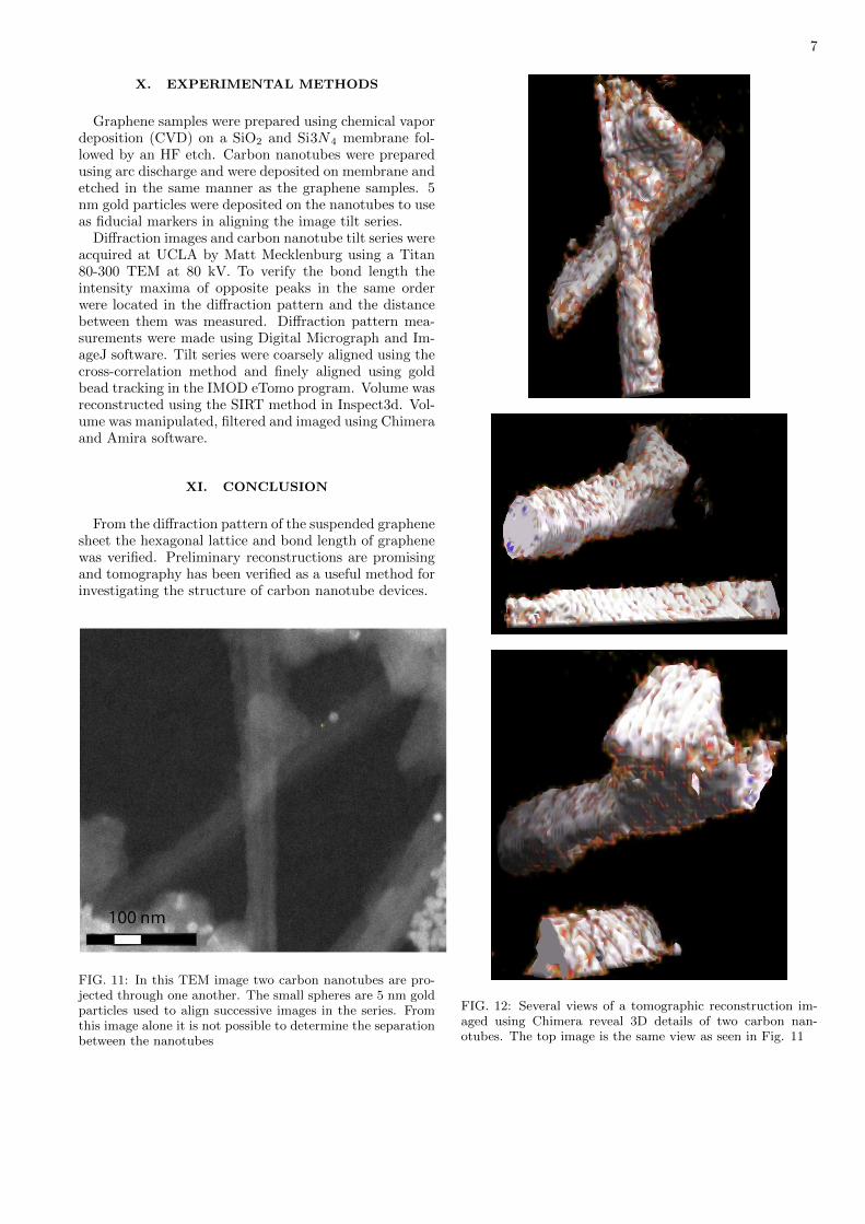
A section of the carbon nanotube tilt series is shown inFig. 11. In this image the two nanotubes are projectedthrough one another and the vertical orientation of thetubes is unclear. After reconstruction the relative posi-tion of the tubes becomes apparent as illustrated in Fig.12.
7
X. EXPERIMENTAL METHODS
Graphene samples were prepared using chemical vapordeposition (CVD) on a SiO2 and Si3N4 membrane fol-lowed by an HF etch. Carbon nanotubes were preparedusing arc discharge and were deposited on membrane andetched in the same manner as the graphene samples. 5nm gold particles were deposited on the nanotubes to useas fiducial markers in aligning the image tilt series.
Diffraction images and carbon nanotube tilt series wereacquired at UCLA by Matt Mecklenburg using a Titan80-300 TEM at 80 kV. To verify the bond length theintensity maxima of opposite peaks in the same orderwere located in the diffraction pattern and the distancebetween them was measured. Diffraction pattern mea-surements were made using Digital Micrograph and Im-ageJ software. Tilt series were coarsely aligned using thecross-correlation method and finely aligned using goldbead tracking in the IMOD eTomo program. Volume wasreconstructed using the SIRT method in Inspect3d. Vol-ume was manipulated, filtered and imaged using Chimeraand Amira software.
XI. CONCLUSION
From the diffraction pattern of the suspended graphenesheet the hexagonal lattice and bond length of graphenewas verified. Preliminary reconstructions are promisingand tomography has been verified as a useful method forinvestigating the structure of carbon nanotube devices.
FIG. 11: In this TEM image two carbon nanotubes are pro-jected through one another. The small spheres are 5 nm goldparticles used to align successive images in the series. Fromthis image alone it is not possible to determine the separationbetween the nanotubes
FIG. 12: Several views of a tomographic reconstruction im-aged using Chimera reveal 3D details of two carbon nan-otubes. The top image is the same view as seen in Fig. 11

8
XII. SUGGESTIONS FOR FURTHERRESEARCH
I was unable to obtain fully suspended graphene sam-ples of a sufficient size to do tomography this summer.Further research will involve doing tomography on a sus-pended sheet of graphene in order to observe it’s char-acteristic ripples. We will then look at how the ripplesare distributed on the sheet. The various amplitudes andwave lengths will be put on a histogram and we will at-tempt to fit the distribution to a Gaussian or Lorentzianfunction. Also we will tomographically reconstruct car-bon nanotube light bulbs to gain insight on the structuralchanges that occur when they radiate.
Given the current limit of tomography it is theoret-ically possible to reconstruct a small carbon nanotubeand resolve individual walls. A resolution of dz = .33nm is possible in reconstructing an object of diameter
D = 15nm using N = 141 views. This corresponds toa tilt increment of θ = 1o and a maximum tilt angle ofα = 70o. This resolution is right at the edge of what iscurrently possible given the limitations of our equipmentand is the subject of ongoing investigation.
Acknowledgments
I would like to thank Matt Mecklenburg for all his guid-ance, time and patience this summer. Also thanks toProfessor Regan and the rest of his lab for allowing meto join their research team. Thanks to the Hong Zho labfor tomography help and allowing me to use their facil-ities. Thanks are also due to the NSF for funding thisproject. Finally I would like to thank Francoise Quevalfor all her work in making the 2010 UCLA REU programrun smoothly.
[1] N.D. Mermin, Physical Review, 176, 250 (1968).[2] A. Fasolino, J.H. Los and M.I. Katsnelson, Nature Ma-
terials 6, 858 (2007).[3] J.C. Meyer et al., Nature 446, 60 (2007).[4] A.K. Geim and K.S. Novoselov, Nature Materials 6, 183
(2007).[5] B.W. Smith and D.E. Luzzia, Journal of Applied Physics
90(7), 3509 (2001).[6] A. Zobelli A. Gloter C.P. Ewels G. Seifert and C. Colliex,
Physical Review B 75 (2007).[7] L. Reimer Transmission Electron Microscopy (Springer
,2009)[8] P. Delhaes, Graphite and Precursors (CRC Press, 2001).[9] C. Kittel, Introduction to Solid State Physics (John Wiley
& Sons, Hoboken, 2005).[10] N.W. Ashcroft and N.D Mermin, Solid State Physics
(Thompson, 1976).[11] P.R. Bevington and D.K. Robinson, Data Reduction and
Error Analysis for the Physical Sciences (McGraw Hill2003).
[12] R.A. Crowther, D.J DeRosier and A. Klug, Proc. Roy.Soc. Lond. A. 317, 319 (1970).
[13] J.C. Russ, The Image Processing Handbook (CRC Press,Boca Raton, 2007).
[14] R. Guckenburger, Ultramicroscopy 9, 167, (1982).[15] Technical details of these algorithms are not very im-
portant for the research presented but it is important toknow that the SIRT method creates more accurate re-constructions than the WBP method.
[16] P.A. Midgley, M. Weyland, Ultramicroscopy 96, 413(2003).