structure dependent optoelectronic properties of monolayer
TRANSCRIPT

This journal is© the Owner Societies 2019 Phys. Chem. Chem. Phys., 2019, 21, 7907--7917 | 7907
Cite this:Phys.Chem.Chem.Phys.,
2019, 21, 7907
Structure dependent optoelectronic propertiesof monolayer antimonene, bismuthene and theirbinary compound
D. Kecik,a V. O. Ozçelik, b E. Durgun *c and S. Ciraci*a
Two-dimensional (2D) antimonene, bismuthene, and their binary compound 2D BiSb possess high spin–orbit
coupling (SOC) and potential topological insulator properties upon engineering their structural and chemical
properties. Based on many-body first-principles calculations, we show that these materials can exhibit
isotropic or anisotropic optoelectronic properties depending on their geometry, i.e. buckled (hb) or
asymmetrical washboard (aw) phases. SOC significantly alters their optoelectronic properties, which is
predominantly evident in 2D bismuthene. hb-antimonene absorbs light in the visible and partially in the
ultraviolet regimes, while the absorption band edge for aw-antimonene, hb- and aw-bismuthene is set at the
infrared region, absorption being spread as a broadband optical response through the spectral range.
An exciton binding with 0.18 eV energy is detected for hb-bismuthene. Due to their broadband optical
response, antimonene, bismuthene, and their binary compound offer possibilities towards applications as
2D materials in solar cells, light-emitting devices, photodetectors and light modulation.
Introduction
Numerous theoretical and experimental studies have revealedcrucial features in the electronic structures of suspendedmonolayers and overlayers of two-dimensional (2D) materialslike graphene,1 transition metal dichalcogenides,2–6 as wellas elemental/compound semiconductors,7–11 and hetero-structures12–14 promising for future optoelectronic applications.The synthesis of 2D ultrathin films of black phosphorus from itsparent layered crystal, and fabrication of a field effect transistorusing micrometer sized phosphorene flakes,15 has brought 2Dallotropes of group-VA elements into focus. On the theoreticalfront it did not take long to prove that all of the group-VAelements (N, P, As, Sb and Bi) can form stable, free-standing 2Dstructures named as nitrogene,16 phosphorene,17 arsenene,18–20
antimonene20–22 and bismuthene.20,23,24 It was shown that each ofthese structures can possess one or more of the hexagonalbuckled (hb), symmetric washboard (sw), asymmetric washboard(aw) or square-octagon (so) phases. All of these structures, whichare also called pnictogens, were predicted to be semiconductors
that can offer promising features suitable for 2D electronics andoptics.25
Among the pnictogens, antimonene and bismuthene gainedparticular importance for the following reasons: (i) the energyrange of antimonene’s fundamental band gap, which isB0.3–2.2 eV, keeps the promise of potential applications in2D electronic and optical nanodevices.21,26–31 (ii) Buckled anti-monene nanoribbons are semiconductors, and their band gapsvary with their chirality and width.32,33 Similarly, the band gapof nanoribbons with the aw structure vary also with their width,offering tunability of the band gap. (iii) Sb and Bi elements canform a stable single-layer (SL) binary compound, which is asemiconductor with a fundamental band gap different fromthe parent constituents. Additionally, this compound exhibitstopologically non-trivial behavior under specific conditions.34,35
(iv) Bi possesses considerable spin–orbit coupling. While three-dimensional (3D) hexagonal Bi crystal with a small direct bandgap and inverted indirect band gap is a semimetal, it becomes atopological insulator under strain.36 Monolayer hb-bismutheneis topologically non-trivial based on the density functionaltheory (DFT)-spin–orbit coupling (SOC) calculations.37 Also,hb-Bi placed on a Si substrate was shown to be topologicallynon-trivial. DFT-SOC calculations of aw-Bi indicated a trivialtopological order.37 (v) Finally, significant progress has beenmade towards the synthesis of SL antimonene and bismuthenestructures. Ultrathin films of antimonene have been synthe-sized using methods such as mechanical/liquid-phase exfolia-tion or epitaxial growth.38–40 2D bismuthene was realized on a
a Department of Physics, Bilkent University, Ankara 06800, Turkey.
E-mail: [email protected] Andlinger Center for Energy and the Environment Princeton University, Princeton,
New Jersey 08544, USAc UNAM – National Nanotechnology Research Center and Institute of Materials
Science and Nanotechnology, Bilkent University, Ankara 06800, Turkey.
E-mail: [email protected]
Received 29th November 2018,Accepted 14th March 2019
DOI: 10.1039/c8cp07344a
rsc.li/pccp
PCCP
PAPER
Publ
ishe
d on
14
Mar
ch 2
019.
Dow
nloa
ded
by B
ilken
t Uni
vers
ity o
n 11
/19/
2019
8:2
7:51
AM
.
View Article OnlineView Journal | View Issue

7908 | Phys. Chem. Chem. Phys., 2019, 21, 7907--7917 This journal is© the Owner Societies 2019
SiC substrate, where wide fundamental band gaps and signifi-cant SOC effects were observed.41
Building on the aforementioned properties of SL Sb and Bi,it is possible to form a compound of these two elements inorder to achieve superior optoelectronic properties, and obtainnew target materials by inverse design; a concept that has beengaining growing attention.42 In fact, BiSb is already present innature in a layered bulk crystal form, from which single layersof BiSb can be exfoliated, according to the previous theoreticalstudies.43,44 2D BiSb is particularly interesting due to the factthat both SL bismuthene and antimonene show high SOC,a precondition of stable topological insulators.35 Hence it iscrucial to have a complete understanding of the electronic andoptical properties of such compounds for future applications.
Current state of the problem
The optical properties of antimonene and bismuthene havebeen studied, with a predominant emphasis on theformer.25,28,30,31,45,46 Alongside the DFT28 and hybrid func-tional (HSE) calculations (with random-phase approximation(RPA) employed subsequently) of hb- and aw-antimonene,30
Shu et al.31 studied the optical properties of hb-antimoneneusing a many-body approach, under the effects of electric fieldand strain. They reported that a strong electric field closed theband gap of aw-Sb and an increasing strain level resulted in ared-shift of the optical spectra, with enhanced optical absorp-tion within 1.2–2.2 eV. They found the G0W0 band gap to beindirect and 2.25 eV, and an exciton binding energy of 0.73 eVwas calculated. The optical properties of monolayer hb-Sb canalso be tuned via surface charge doping by p/n type surfacedopants, which revealed enhanced absorption of light espe-cially in the early photon energy regime.45 In a recent studyemploying the many-body Green’s function approach, thefundamental band gap of hb-Sb was predicted as 2.38 eV.Moreover, the optical and luminescence band gaps of SLhb-Sb were found to be 2.3/1.5 eV, resulting in an excitonbinding energy of 0.8 eV.46 Promising indications of anti-monene’s broadband use as a photodetector or opticalmodulator have been shown recently.47,48
Bismuthene’s optical properties have not been vastly inves-tigated yet, with only a few recent examples of electric fieldapplications or its potential as a photonic-based device,45,49–51
hence the light-matter interaction within 2D bismutheneremains an area of interest. While the dynamical stability,electronic structure and topological features of SL BiSb binarycompounds have been studied actively,34,35,52–56 very little isknown about their optical properties. Stable binary compoundsof 2D BiSb were systematically investigated from first-principlesby Xiao et al.,52 who found few stable aw-BiSb alloy structures,one of them having a direct HSE band gap of 0.43 eV. Regardingthe effects of strain on the electronic band structure andstability of SL BiSb, the compound turned out to be a semi-conductor with a direct band gap as well, reducing understrain, and undergoing a direct–indirect-metal transition whencompressive strain is applied.53 With the inclusion of SOC in SLhb-BiSb, a Rashba spin-splitting of 13 meV near the Fermi level
was observed, which can be tuned by in-plane biaxial strain,making this material a candidate for efficient spin field-effecttransistors, optoelectronics, and spintronic devices.34 The samematerial was predicted to be a quantum spin Hall insulatorunder biaxial strain.54
In this paper, by performing first-principles calculations andincorporating many-body interactions, we show that SL hb andaw phases of Sb and Bi, as well as 2D BiSb, display opticalactivities that span the infrared (IR), visible and ultraviolet (UV)light regimes partially or entirely, and exhibit either an iso-tropic or anisotropic optical response depending on theirgeometrical phases. We present a complete analysis of theoptoelectronic properties of 2D Sb and Bi which also shed lighton the possible functionalities of their compounds. We calculatethese properties using the HSE–SOC + RPA approach, i.e. employingRPA on top of the HSE ground state calculations with spin–orbitcoupling effects taken into account. Moreover, we report theHSE–SOC and G0W0 band gaps of all pristine structures. Finally,we investigate the excitonic effects within the optical propertiesof two representative materials, hb-Sb and hb-Bi.
Methodology
The ground-state electronic structure calculations were performedfor the 2D hb- and aw-structures of Sb and Bi, using spin-polarized DFT. The projector-augmented-wave potentials (PAW)formalism57–59 implemented in the VASP code60,61 was used.The electron exchange and correlation (XC) potential wasdescribed by the Perdew–Burke–Ernzerhof (PBE) form withinthe generalized gradient approximation (GGA), with XC correla-tion potential parameters tuned according to GW parameters.62
The plane-wave basis set was used with an energy cutoff of 520eV for all calculations. Atomic positions were optimized usingthe conjugate gradient method by minimizing the total energyand atomic forces. The energy difference between the sequen-tial steps was set to 10�6 eV for convergence. The maximumallowed force on each atom and Gaussian smearing factor weretaken as 0.05 eV �1 and 0.05 eV, respectively. A G-centered127 � 127 � 1 grid was employed for the Brillouin zone (BZ)integration of the primitive unit cells. In order to avoid spuriousinteractions between the periodic images, a supercell withminimum B20 Švacuum space was adopted.
Subsequent to the lattice optimizations, hybrid functionals(HSE06)63–65 and the quasiparticle (QP) non-self consistentG0W0 approach [(QP)G0W0],66–68 where G and W are iteratedonce, were used (without further ionic relaxation) to obtain thecorrected band structures and optical spectra of hb-Sb, hb-Bi,aw-Sb, and aw-Bi. The updated wavefunctions given by HSE areused as a basis for the (QP)G0W0 calculations. RPA69,70 wasemployed on top of the HSE and G0W0 approaches, using a totalof 192 (valence and conduction) bands. Due to the heavycomputational workload, the k-mesh was reduced to 19 � 19 �1 and 13 � 13 � 1 for hb- and aw-structures, respectively, whilecalculating the quasiparticle band energies. The screening wasevaluated at 240 frequency points for the majority of the (QP)G0W0
Paper PCCP
Publ
ishe
d on
14
Mar
ch 2
019.
Dow
nloa
ded
by B
ilken
t Uni
vers
ity o
n 11
/19/
2019
8:2
7:51
AM
. View Article Online

This journal is© the Owner Societies 2019 Phys. Chem. Chem. Phys., 2019, 21, 7907--7917 | 7909
calculations. The plane-wave cutoff was decreased to 350 eV andthe basis set for the response functions was set to 240 eV for theG0W0 calculations. Local field effects were accounted for both atthe levels of Hartree and exchange–correlation potential. The SOCeffects were included self-consistently by rotating all spins withrespect to the spin quantization axis (0,0,1), both at the levels ofPBE and HSE.71 For all structures, the SOC effects were incorpo-rated continuously, during the steps of lattice optimization andcomputation of the RPA spectra.
Regarding the optical response beyond the independent-particle approach, the electron–hole interactions were takeninto account by solving the Bethe–Salpeter equation (BSE)72–74
within the Tamm–Dancoff approximation, using the samek-point sampling, energy cutoff value and number of bandsas in the (QP)G0W0 calculation.75 The excitonic effects wereconsidered by including the eight highest occupied valence andten lowest unoccupied conduction bands. Further to the mainoptical response function, the frequency dependent imaginarydielectric function e2(o), layer dependent absorbance [A(o)] canbe obtained through the relation: A(o) = oLe2(o)/c, L beingthe distance between two periodic images of the 2D materialand c the speed of light.
2D antimonene and bismutheneAtomic and electronic structures
In recent theoretical studies,20,23,76,77 three stable phases,namely hexagonal buckled (hb- or b-phase), asymmetric wash-board (aw- or a-phase), and square-octagon (so-), of 2D anti-monene and bismuthene were suggested. On the other hand,the symmetric washboard (sw) structure, which is a stablephase for phosphorene and arsenene, is destabilized for anti-monene and bismuthene. In the present study, we consideronly the hb- and aw-phases as described in Fig. 1, and calculatetheir optimized atomic structure and self-consistent fieldelectronic band structure for the sake of completeness, whichconstitute the basis for the present study of the optical properties.
Optimized structural parameters, such as 2D lattice con-stants a and b, bond lengths d1 and d2, and buckling parameterD, are presented in Table 1. Electronic energy structures ofthese 2D monolayers are calculated firstly within PBE–SOC, andsubsequently corrected by HSE–SOC and G0W0. The standardDFT calculations incorporating SOC effects are performed onlyin order to provide a basis for band gap comparisons, and areout of scope in terms of the optical properties. The calculatedfundamental band gaps together with the results of earliercalculations are also listed in Table 1. According to the HSE–SOC calculations, hb-Sb is an indirect band gap semiconductorwith a band gap of 1.12 eV, in comparison to the 0.78 eVindirect PBE–SOC gap. This gap is predicted as 1.57 eV from theG0W0 calculations. The direct fundamental band gap of aw-Sb isrelatively smaller and calculated as 0.16, 0.23 and 0.37 eV fromthe PBE–SOC, HSE–SOC and G0W0 calculations, respectively.Using the HSE–SOC (PBE–SOC) approach, we predict thefundamental (indirect) band gap of hb-Bi and aw-Bi structures
as 0.45 (0.33) and 0.25 (0.14) eV, respectively. These valuesincrease to 0.92 and 0.35 eV as a result of the G0W0 calculations.In Fig. 2, the band structures of hb-Sb, aw-Sb, hb-Bi and aw-Bicalculated from HSE–SOC are presented. The fundamentalband gaps calculated from G0W0 are also shaded in the samefigure.
Optical absorption spectra
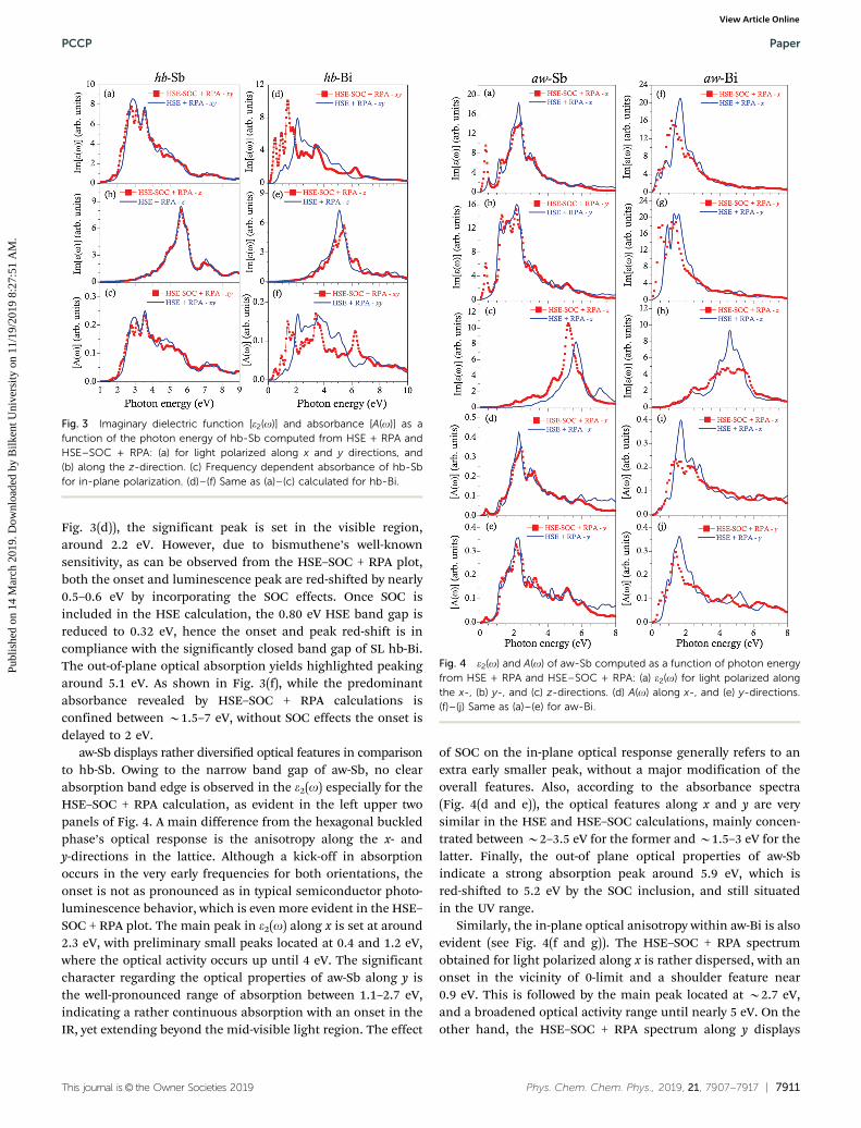
SL antimonene and bismuthene structures’ electronic bandgaps lie within a certain range, as discussed in the previoussection. This diversity in between the IR and visible regimes isquite promising in terms of their optical properties. Topo-logical features displayed by a few of the phases promisefurther interesting implications for the optical spectra. In thefollowing discussions, we present our findings regarding thelinearly polarized optical response to normal incident light,obtained from the frequency dependent imaginary dielectricfunction (e2(o)) and layer-dependent absorbance (A(o)) plots.The optical spectra of the hb and aw phases of SL Sb and Bicomputed using the HSE + RPA approach are shown in Fig. 3and 4. In this section we also highlight the effects of SOC on theoptical response of SL Sb and Bi. We then extend our discussionby including the many-body effects. Due to the shortcomings ofthe standard DFT method for calculating the excited state properties,we do not include this approach in the discussion herewith.
As presented in Fig. 3(a), a main luminescence peak in theHSE + RPA in-plane optical response (i.e. light polarized alongx, y directions) for the hb-Sb phase is observed near 2.8 eV,where the onset is located slightly below 2 eV and the rangeof this predominant absorption phenomenon is betweenB2.4–3.9 eV. The optical activity of hb-Sb continues furtheruntil 6 eV. Hence, the hb-phase of 2D Sb can be considered as asignificant candidate SL material for devices operating underboth visible and UV light. Regarding the out-of-plane response,i.e. light polarized along the z-axis (see Fig. 3(b)), a main singleluminescence peak appears at 5.7 eV, thus indicating a
Fig. 1 (a) Top and side views of hb- (or b-phase) and (b) aw- (or a-phase)structures of antimonene and bismuthene. The primitive unit cell vectorsare designated by the lattice constants a and b. The buckling parameter Dand bond length d of the hb-structure, and two different bond lengths d1
and d2 of the aw-structure, are also shown.
PCCP Paper
Publ
ishe
d on
14
Mar
ch 2
019.
Dow
nloa
ded
by B
ilken
t Uni
vers
ity o
n 11
/19/
2019
8:2
7:51
AM
. View Article Online

7910 | Phys. Chem. Chem. Phys., 2019, 21, 7907--7917 This journal is© the Owner Societies 2019
different character of optical features with respect to thein-plane optical response.
The SOC effect on the optical properties of hb-Sb, asdisplayed in the e2(o) and A(o) plots in Fig. 3(a–c), is observedto be minor. Only a slight red-shift of the optical absorptionband edge occurs once SOC is taken into account. The differ-ences at the highest amplitude of the luminescence peaks arisefrom the computational artifacts. Referring to the HSE andHSE–SOC band gaps of hb-Sb near 1.2 eV, the minor onsetshifts between both approaches are expected. The in-plane
absorbance presented in the lower left panel shows that themain optical activity is concentrated between 2.5–6 eV. A furthercomment on a method-wise comparison, regarding the time-dependent Hartree Fock approach to calculating the opticalspectra, is that only minor differences from the HSE–RPA spectraof SL hb-, aw-Sb and hb-, aw-Bi structures were observed.
SL hb-Bi, with an isotropic in-plane optical response, alsocomes out as an interesting 2D material in terms of its linearoptical properties. Although the absorption band edge islocated slightly above 0.5 eV (see the HSE + RPA spectrum in
Table 1 Structural parameters (lattice constants a and b, bond lengths d, d1 and d2, and the buckling parameter D, all calculated within LDA or PBE), andelectronic band gaps of the hb and aw phases of antimonene and bismuthene, calculated from PBE–SOC, HSE, HSE–SOC and G0W0
a (Å) b (Å) d, d1 (Å) d2 (Å) D (Å) Eg-PBE/PBE–SOC (eV) Eg-HSE (eV) Eg-HSE–SOC (eV) Eg-G0W0 (eV)
hb-Sb 4.04 4.04 2.87 — 1.67 —/0.78(i) — 1.12(i) 1.57hb-Sb30 4.12 4.12 2.89 — 1.65 1.26/0.99 1.70 — —hb-Sb26 — — — — — 1.26/1.00 — — —hb-Sb21 4.04 4.04 2.87 — 1.67 1.04/0.69 1.55 — —hb-Sb27 4.04 4.04 2.87 — — —/0.76(i) — — —hb-Sb31 3.98 3.98 2.81 — 1.61 1.10(i)/— — — 2.25hb-Sb28,29,46 — — — — — 1.65/— 2.28,29 1.1828 — 2.3846
aw-Sb 4.77 4.28 2.91 2.85 — —/0.16(d) — 0.23(d) 0.37aw-Sb30 4.73 4.36 2.95 2.87 — 0.22/0.21 0.26 — —aw-Sb21 4.74 4.28 2.91 2.84 — 0.16/0.19 0.34 — —aw-Sb27 4.77 4.28 2.91 2.86 — —/0.28 — — —aw-Sb28 — — — — — —/— 0.54 — —hb-Bi 4.18 4.18 3.01 — 1.80 —/0.33(i) — 0.45(i) 0.92hb-Sb26,29,78 — — — — — 0.5526,78/0.43,26 0.5078 0.9929 — —hb-Bi23 4.38 4.38 3.07 — 1.74 —/0.51 0.80 0.32 —aw-Bi 4.89 4.44 3.08 3.02 — —/0.14(i) — 0.25(i) 0.35aw-Bi23 4.94 4.55 3.11 3.10 — —/0.28 0.23 0.39 —hb-Bi29 — — — — — —/— 0.36 — —hb-BiSb 4.12 4.12 2.95 — 1.73 —/—/0.16(i) 1.21(i) 0.51(i) —hb-BiSb52 4.24 4.24 — — 1.67 —/— 1.48(d) — —aw-BiSb 4.80 4.37 3.00 2.95 — —/0.15(i) 0.53(i) 0.24(i) —aw-BiSb52 4.81 4.46 — — 3.35 —/— 0.43(d) — —
Fig. 2 The electronic band structure of SL hb-Sb, aw-Sb, hb-Bi and aw-Bi computed from HSE–SOC. G0W0 band gaps are shown by the shaded area.Red arrows indicate the fundamental band gaps. The zero energy is set at the top of the valence bands and Brillouin zones are shown by the insets.
Paper PCCP
Publ
ishe
d on
14
Mar
ch 2
019.
Dow
nloa
ded
by B
ilken
t Uni
vers
ity o
n 11
/19/
2019
8:2
7:51
AM
. View Article Online
This journal is© the Owner Societies 2019 Phys. Chem. Chem. Phys., 2019, 21, 7907--7917 | 7911
Fig. 3(d)), the significant peak is set in the visible region,around 2.2 eV. However, due to bismuthene’s well-knownsensitivity, as can be observed from the HSE–SOC + RPA plot,both the onset and luminescence peak are red-shifted by nearly0.5–0.6 eV by incorporating the SOC effects. Once SOC isincluded in the HSE calculation, the 0.80 eV HSE band gap isreduced to 0.32 eV, hence the onset and peak red-shift is incompliance with the significantly closed band gap of SL hb-Bi.The out-of-plane optical absorption yields highlighted peakingaround 5.1 eV. As shown in Fig. 3(f), while the predominantabsorbance revealed by HSE–SOC + RPA calculations isconfined between B1.5–7 eV, without SOC effects the onset isdelayed to 2 eV.
aw-Sb displays rather diversified optical features in comparisonto hb-Sb. Owing to the narrow band gap of aw-Sb, no clearabsorption band edge is observed in the e2(o) especially for theHSE–SOC + RPA calculation, as evident in the left upper twopanels of Fig. 4. A main difference from the hexagonal buckledphase’s optical response is the anisotropy along the x- andy-directions in the lattice. Although a kick-off in absorptionoccurs in the very early frequencies for both orientations, theonset is not as pronounced as in typical semiconductor photo-luminescence behavior, which is even more evident in the HSE–SOC + RPA plot. The main peak in e2(o) along x is set at around2.3 eV, with preliminary small peaks located at 0.4 and 1.2 eV,where the optical activity occurs up until 4 eV. The significantcharacter regarding the optical properties of aw-Sb along y isthe well-pronounced range of absorption between 1.1–2.7 eV,indicating a rather continuous absorption with an onset in theIR, yet extending beyond the mid-visible light region. The effect
of SOC on the in-plane optical response generally refers to anextra early smaller peak, without a major modification of theoverall features. Also, according to the absorbance spectra(Fig. 4(d and e)), the optical features along x and y are verysimilar in the HSE and HSE–SOC calculations, mainly concen-trated between B2–3.5 eV for the former and B1.5–3 eV for thelatter. Finally, the out-of plane optical properties of aw-Sbindicate a strong absorption peak around 5.9 eV, which isred-shifted to 5.2 eV by the SOC inclusion, and still situatedin the UV range.
Similarly, the in-plane optical anisotropy within aw-Bi is alsoevident (see Fig. 4(f and g)). The HSE–SOC + RPA spectrumobtained for light polarized along x is rather dispersed, with anonset in the vicinity of 0-limit and a shoulder feature near0.9 eV. This is followed by the main peak located at B2.7 eV,and a broadened optical activity range until nearly 5 eV. On theother hand, the HSE–SOC + RPA spectrum along y displays
Fig. 3 Imaginary dielectric function [e2(o)] and absorbance [A(o)] as afunction of the photon energy of hb-Sb computed from HSE + RPA andHSE–SOC + RPA: (a) for light polarized along x and y directions, and(b) along the z-direction. (c) Frequency dependent absorbance of hb-Sbfor in-plane polarization. (d)–(f) Same as (a)–(c) calculated for hb-Bi.
Fig. 4 e2(o) and A(o) of aw-Sb computed as a function of photon energyfrom HSE + RPA and HSE–SOC + RPA: (a) e2(o) for light polarized alongthe x-, (b) y-, and (c) z-directions. (d) A(o) along x-, and (e) y-directions.(f)–(j) Same as (a)–(e) for aw-Bi.
PCCP Paper
Publ
ishe
d on
14
Mar
ch 2
019.
Dow
nloa
ded
by B
ilken
t Uni
vers
ity o
n 11
/19/
2019
8:2
7:51
AM
. View Article Online
7912 | Phys. Chem. Chem. Phys., 2019, 21, 7907--7917 This journal is© the Owner Societies 2019
relatively concentrated and pronounced peaks within B0.4–2 eV.The SOC effects red-shift the optical spectra, due to the closingband gaps. The out-of-plane response displays that without SOC,a distinct peak is observed at 4.75 eV, however including SOCleads to a dispersed spectral distribution of absorption. Finally,as can be observed in Fig. 4(i and j), the anisotropic absorbanceplots of aw-Bi show that the absorbance along x is confinedbetween B1–3.5 eV, and along y within a slightly narrower scale;peaking roughly at 1.7 eV.
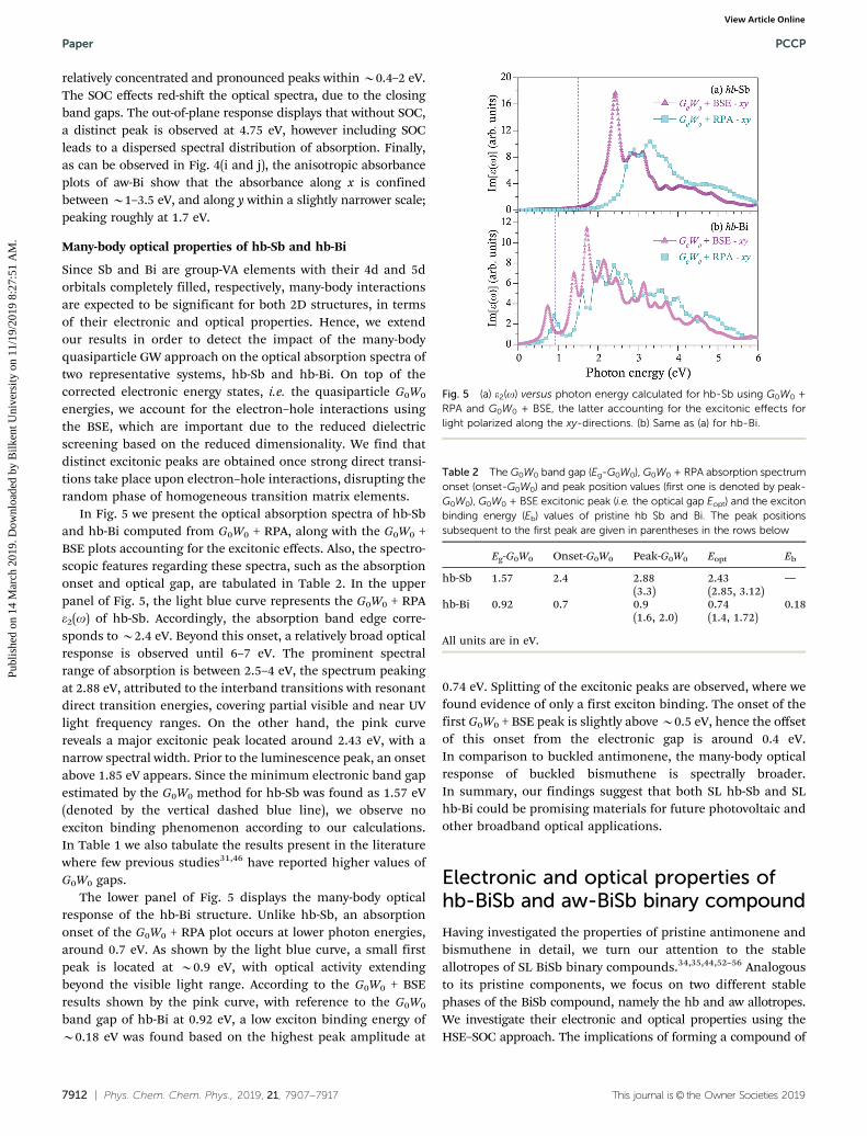
Many-body optical properties of hb-Sb and hb-Bi
Since Sb and Bi are group-VA elements with their 4d and 5dorbitals completely filled, respectively, many-body interactionsare expected to be significant for both 2D structures, in termsof their electronic and optical properties. Hence, we extendour results in order to detect the impact of the many-bodyquasiparticle GW approach on the optical absorption spectra oftwo representative systems, hb-Sb and hb-Bi. On top of thecorrected electronic energy states, i.e. the quasiparticle G0W0
energies, we account for the electron–hole interactions usingthe BSE, which are important due to the reduced dielectricscreening based on the reduced dimensionality. We find thatdistinct excitonic peaks are obtained once strong direct transi-tions take place upon electron–hole interactions, disrupting therandom phase of homogeneous transition matrix elements.
In Fig. 5 we present the optical absorption spectra of hb-Sband hb-Bi computed from G0W0 + RPA, along with the G0W0 +BSE plots accounting for the excitonic effects. Also, the spectro-scopic features regarding these spectra, such as the absorptiononset and optical gap, are tabulated in Table 2. In the upperpanel of Fig. 5, the light blue curve represents the G0W0 + RPAe2(o) of hb-Sb. Accordingly, the absorption band edge corre-sponds to B2.4 eV. Beyond this onset, a relatively broad opticalresponse is observed until 6–7 eV. The prominent spectralrange of absorption is between 2.5–4 eV, the spectrum peakingat 2.88 eV, attributed to the interband transitions with resonantdirect transition energies, covering partial visible and near UVlight frequency ranges. On the other hand, the pink curvereveals a major excitonic peak located around 2.43 eV, with anarrow spectral width. Prior to the luminescence peak, an onsetabove 1.85 eV appears. Since the minimum electronic band gapestimated by the G0W0 method for hb-Sb was found as 1.57 eV(denoted by the vertical dashed blue line), we observe noexciton binding phenomenon according to our calculations.In Table 1 we also tabulate the results present in the literaturewhere few previous studies31,46 have reported higher values ofG0W0 gaps.
The lower panel of Fig. 5 displays the many-body opticalresponse of the hb-Bi structure. Unlike hb-Sb, an absorptiononset of the G0W0 + RPA plot occurs at lower photon energies,around 0.7 eV. As shown by the light blue curve, a small firstpeak is located at B0.9 eV, with optical activity extendingbeyond the visible light range. According to the G0W0 + BSEresults shown by the pink curve, with reference to the G0W0
band gap of hb-Bi at 0.92 eV, a low exciton binding energy ofB0.18 eV was found based on the highest peak amplitude at
0.74 eV. Splitting of the excitonic peaks are observed, where wefound evidence of only a first exciton binding. The onset of thefirst G0W0 + BSE peak is slightly above B0.5 eV, hence the offsetof this onset from the electronic gap is around 0.4 eV.In comparison to buckled antimonene, the many-body opticalresponse of buckled bismuthene is spectrally broader.In summary, our findings suggest that both SL hb-Sb and SLhb-Bi could be promising materials for future photovoltaic andother broadband optical applications.
Electronic and optical properties ofhb-BiSb and aw-BiSb binary compound
Having investigated the properties of pristine antimonene andbismuthene in detail, we turn our attention to the stableallotropes of SL BiSb binary compounds.34,35,44,52–56 Analogousto its pristine components, we focus on two different stablephases of the BiSb compound, namely the hb and aw allotropes.We investigate their electronic and optical properties using theHSE–SOC approach. The implications of forming a compound of
Fig. 5 (a) e2(o) versus photon energy calculated for hb-Sb using G0W0 +RPA and G0W0 + BSE, the latter accounting for the excitonic effects forlight polarized along the xy-directions. (b) Same as (a) for hb-Bi.
Table 2 The G0W0 band gap (Eg-G0W0), G0W0 + RPA absorption spectrumonset (onset-G0W0) and peak position values (first one is denoted by peak-G0W0), G0W0 + BSE excitonic peak (i.e. the optical gap Eopt) and the excitonbinding energy (Eb) values of pristine hb Sb and Bi. The peak positionssubsequent to the first peak are given in parentheses in the rows below
Eg-G0W0 Onset-G0W0 Peak-G0W0 Eopt Eb
hb-Sb 1.57 2.4 2.88 2.43 —(3.3) (2.85, 3.12)
hb-Bi 0.92 0.7 0.9 0.74 0.18(1.6, 2.0) (1.4, 1.72)
All units are in eV.
Paper PCCP
Publ
ishe
d on
14
Mar
ch 2
019.
Dow
nloa
ded
by B
ilken
t Uni
vers
ity o
n 11
/19/
2019
8:2
7:51
AM
. View Article Online

This journal is© the Owner Societies 2019 Phys. Chem. Chem. Phys., 2019, 21, 7907--7917 | 7913
Sb and Bi on the resulting optoelectronic properties could shedlight on the increased functionalities of both materials.
The electronic band diagrams of the hb- and aw-BiSb binarycompounds are displayed in Fig. 6. Both structures were foundto be narrow and indirect band gap systems, the former phasewith a HSE–SOC indirect band gap of 0.51, and 0.24 eV for thelatter, both values much closer to that of pristine bismuthenerather than antimonene. The closing of the HSE gaps due to theSOC effects were found as 0.7 and 0.3 eV for the hb-BiSb andaw-BiSb structures, respectively. Regarding the optical proper-ties computed from HSE + RPA, as shown in Fig. 7, a sharp risein the in-plane absorption of hb-BiSb occurs around 1.2 eV witha luminescence peak located at 2.5 eV, and optical activityextending until nearly 5 eV (see the uppermost panel). Theabsorption band edge, main peak positions and significantoptical absorption range of hb-BiSb resemble those revealed bySL hb-Bi in comparison to hb-Sb, with an onset in the IR andmain peak in the visible regimes. On the other hand, the out-of-plane optical response (see Fig. 7(b)) indicates main absorptionpeaking at B5.4 eV. When SOC effects are included, an extra,small early peak of the in-plane absorption appears at 0.8 eV,followed by a more distinct peak at 2.1 eV. In addition, a red-shiftof the overall spectrum is observed owing to the closed band gap,once SOC effects are taken into account.
With regard to the optical response of aw-BiSb (see Fig. 7(c–e))computed from HSE + RPA, a small shoulder after 0.5 eV forlight polarized along the x-direction, and a main peak withhighest amplitude at nearly 2 eV are observed. On the otherhand, the HSE–SOC + RPA plot reveals an earlier narrow peak at0.38 eV, and then a larger peak with the highest amplitude at1.71 eV. The anisotropy within the HSE + RPA in-plane optical
response is evident from the rather enlarged absorption peakalong the y-direction, concentrated between B0.8–3 eV. TheHSE–SOC + RPA spectrum along y yields again an extra low-frequency shoulder, along with a major absorption peakappearing at 1.67 eV. The optical activity is pursued until nearly3 eV for both orientations of the in-plane absorption. Hence,the BiSb compound in the asymmetric washboard structuredisplays significant optical features within the IR and visibleregimes. Concerning the SOC effects, the global red-shift ofe2(o) is also valid for aw-BiSb, due to the reduced HSE–SOCband gap. Finally, the out-of-plane optical spectrum of aw-BiSbdisplays a distinct HSE + RPA peak at B5.2 eV, which isdispersed between 4.3–5.4 eV in the case of the HSE–SOC +RPA approach.
Fig. 6 The electronic energy band structures of the SL hb-BiSb andaw-BiSb binary compounds computed from HSE–SOC.
Fig. 7 e2(o) as a function of photon energy of the hb-BiSb compoundcalculated from HSE + RPA and HSE–SOC + RPA, (a) for light polarizedalong the x and y, and (b) z-directions. e2(o) of the aw-BiSb compoundcalculated from HSE + RPA and HSE–SOC + RPA, for light polarized alongthe (c) x-, (d) y-, and (e) z-directions.
PCCP Paper
Publ
ishe
d on
14
Mar
ch 2
019.
Dow
nloa
ded
by B
ilken
t Uni
vers
ity o
n 11
/19/
2019
8:2
7:51
AM
. View Article Online

7914 | Phys. Chem. Chem. Phys., 2019, 21, 7907--7917 This journal is© the Owner Societies 2019
Discussions and conclusions
In conclusion, we report that 2D antimonene and bismuthenestructures with fundamental band gaps near the IR and visiblelight regions have promising optoelectronic properties for futurebroadband photonic and light modulator device applications.According to the HSE results, for hb-Sb, prominent opticalabsorption occurs within the visible regime with an onset ofabsorption at B2 eV and within the IR for hexagonal buckledBi. For both structures, the optical activity extends beyond thevisible light range. On the other hand, for all other phases excepthb-Sb, absorption begins to be active in the IR region. From theaspect of many-body effects, a systematic blue-shift of the spectralfeatures from HSE–SOC + RPA to the quasiparticle G0W0 + RPAcalculations is observed. A major excitonic peak for hb-Sb isobserved slightly above 2.4 eV, where no apparent exciton bindingis evident. In summary, hb-Sb can be considered as a significantcandidate SL material for devices operating under both visibleand UV light. The SOC effects on the optical properties of hb-Sbare observed to be minor. Regarding the main HSE–SOC + RPApeak along the e2(o) of aw-Sb, the prominent peak is set at around2.3 eV, and the spectral features are active until 4 eV. Along theother in-plane crystalline orientation of aw-Sb, the well-pronounced range of absorption is between 1.1–2.7 eV, indicatinga rather continuous absorption with an onset in the IR, andextending beyond the mid-visible light region. In view of effectivesolar absorption, antimonene stands out with clear luminescencepeaks concentrated in the visible range.
We also show that inclusion of spin–orbit coupling effectsmodifies the optical spectra of bismuthene to a significantextent. Although the absorption onset of hb-Bi is locatedslightly above 0.5 eV, the major peak of absorption is set inthe visible frequencies, around 2.2 eV. On the other hand, boththe absorption onset and luminescence peak are red-shifted byB0.6 eV, when SOC effects are included. The in-plane opticalresponse of hb-Bi is substantially affected once the electron–hole interactions are taken into account, with enhancedabsorption even above the quasiparticle gap. A first excitonbinding with 0.18 eV binding energy is predicted. The aniso-tropic optical absorbance of aw-Bi is rather confined betweenB1–3.5 eV along the x-direction, and within a narrower scalealong y, peaking at B1.7 eV. Similarly, SOC leads to a red-shiftof the optical spectra of aw-Bi, owing to the reduced band gapvalues. In general, the differences in the optical spectra causedby the SOC effects are more distinguished for the Bi phasescompared to Sb. Moreover, the in-plane optical response ismodified upon including the SOC effects, in a more obviousway in comparison to the out-of-plane direction. However, noclear trends regarding the differences in the optical responsealong the x or y-directions were observed.
The optical properties of the SL BiSb structures can either beisotropic or anisotropic, with the possibility of tuning theoptoelectronic properties based on the stoichiometric mixingproportion of Sb and Bi atoms. Due to the small band gapsof the SL BiSb compound, the HSE–SOC + RPA calculationsindicate early in-plane absorption band edges for both structures.
Both the hb- and aw- phases reveal optical activities spanning thevisible regime, and partially extending to the UV range.
In summary, the electronic band gap, optical gap andexciton binding energies can be tuned depending on thedifferent crystalline orientations, which could be useful forlight manipulation or modulation. Furthermore, SOC effectsimpose different levels of alterations in the optoelectronicproperties of SL pristine Sb, Bi and the binary compound BiSb.While we find an exciton binding phenomenon for the buckledphase of bismuthene, many-body effects are still prominentregarding the optoelectronic properties of 2D Sb, Bi and BiSb.We hope that this study will contribute to the knowledgenecessary for next-generation devices based on 2D Sb, Bi andthe BiSb compound, and for exploring new physics in ultrathingroup-VA members.
Conflicts of interest
There are no conflicts to declare.
Acknowledgements
The calculations were performed at TUBITAK ULAKBIM, HighPerformance and Grid Computing Center (TR-Grid e-Infrastructure)and the National Center for High Performance Computing ofTurkey (UHeM) under grant no. 5003622015. This work wassupported by the Scientific and Technological Research Council ofTurkey (TUBITAK) under Project No. 115F088. E. D. acknowledgessupport from The Turkish Academy of Sciences – OutstandingYoung Scientists Award Program (TUBA-GEBIP). S. C. acknowledgesthe financial support from Academy of Science of Turkey (TUBA).
References
1 K. S. Novoselov, A. K. Geim, S. V. Morozov, D. Jiang,Y. Zhang, S. V. Dubonos, I. V. Grigorieva and A. A. Firsov,Electric Field Effect in Atomically Thin Carbon Films,Science, 2004, 306, 666–669.
2 J. N. Coleman, M. Lotya, A. O’Neill, S. D. Bergin, P. J. King,U. Khan, K. Young, A. Gaucher, S. De and R. J. Smith, et al.,Two-dimensional Nanosheets Produced by Liquid Exfolia-tion of Layered Materials, Science, 2011, 331, 568–571.
3 K. Novoselov, D. Jiang, F. Schedin, T. Booth, V. Khotkevich,S. Morozov and A. Geim, Two-dimensional Atomic Crystals,Proc. Natl. Acad. Sci. U. S. A., 2005, 102, 10451–10453.
4 C. Ataca and S. Ciraci, Functionalization of Single-layerMoS2 Honeycomb Structures, J. Phys. Chem. C, 2011, 115,13303–13311.
5 C. Ataca, H. Sahin and S. Ciraci, Stable, Single-layer MX2
Transition-metal Oxides and Dichalcogenides in aHoneycomb-like Structure, J. Phys. Chem. C, 2012, 116,8983–8999.
6 V. O. Ozçelik, M. Fathi, J. G. Azadani and T. Low, TinMonochalcogenide Heterostructures as Mechanically Rigid
Paper PCCP
Publ
ishe
d on
14
Mar
ch 2
019.
Dow
nloa
ded
by B
ilken
t Uni
vers
ity o
n 11
/19/
2019
8:2
7:51
AM
. View Article Online

This journal is© the Owner Societies 2019 Phys. Chem. Chem. Phys., 2019, 21, 7907--7917 | 7915
Infrared Band Gap Semiconductors, Phys. Rev. Mater., 2018,2, 051003.
7 E. Durgun, S. Tongay and S. Ciraci, Silicon and III-VCompound Nanotubes: Structural and Electronic Properties,Phys. Rev. B: Condens. Matter Mater. Phys., 2005, 72, 075420.
8 K. K. Kim, A. Hsu, X. Jia, S. M. Kim, Y. Shi, M. Hofmann,D. Nezich, J. F. Rodriguez-Nieva, M. Dresselhaus andT. Palacios, et al., Synthesis of Monolayer Hexagonal BoronNitride on Cu Foil Using Chemical Vapor Deposition, NanoLett., 2012, 12, 161–166.
9 S. Cahangirov, M. Topsakal and S. Ciraci, Armchair Nano-ribbons of Silicon and Germanium Honeycomb Struc-tures, Phys. Rev. B: Condens. Matter Mater. Phys., 2010,81, 195120.
10 H. Sahin, S. Cahangirov, M. Topsakal, E. Bekaroglu,E. Akturk, R. T. Senger and S. Ciraci, Monolayer HoneycombStructures of Group-IV Elements and III-V BinaryCompounds: First-principles Calculations, Phys. Rev. B:Condens. Matter Mater. Phys., 2009, 80, 155453.
11 D. Kecik, A. Onen, M. Konuk, E. Gurbuz, F. Ersan,S. Cahangirov, E. Akturk, E. Durgun and S. Ciraci, Funda-mentals, Progress, and Future Directions of Nitride-basedSemiconductors and Their Composites in Two-dimensionalLimit: A First-principles Perspective to Recent Synthesis,Appl. Phys. Rev., 2018, 5, 011105.
12 A. Du, In silico engineering of graphene-based van der Waalsheterostructured nanohybrids for electronics and energyapplications, Wiley Interdiscip. Rev.: Comput. Mol. Sci.,2016, 6, 551–570.
13 X. Zhang, Z. Meng, D. Rao, Y. Wang, Q. Shi, Y. Liu, H. Wu,K. Deng, H. Liu and R. Lu, Efficient band structure tuning,charge separation, and visible-light response in ZrS2-basedvan der Waals heterostructures, Energy Environ. Sci., 2016, 9,841–849.
14 P. Wang, S. Liu, W. Luo, H. Fang, F. Gong, N. Guo, Z.-G.Chen, J. Zou, Y. Huang and X. Zhou, et al., Arrayed van derWaals Broadband Detectors for Dual-Band Detection, Adv.Mater., 2017, 29, 1604439.
15 L. Li, Y. Yu, G. J. Ye, Q. Ge, X. Ou, H. Wu, D. Feng,X. H. Chen and Y. Zhang, Black Phosphorus Field-effectTransistors, Nat. Nanotechnol., 2014, 9, 372.
16 V. O. Ozcelik, O. U. Akturk, E. Durgun and S. Ciraci,Prediction of a Two-dimensional Crystalline Structure ofNitrogen Atoms, Phys. Rev. B: Condens. Matter Mater. Phys.,2015, 92, 125420.
17 H. Liu, A. T. Neal, Z. Zhu, Z. Luo, X. Xu, D. Tomanek andP. D. Ye, Phosphorene: An Unexplored 2D Semiconductorwith a High Hole Mobility, ACS Nano, 2014, 8, 4033–4041.
18 C. Kamal and M. Ezawa, Arsenene: Two-dimensionalBuckled and Puckered Honeycomb Arsenic Systems, Phys.Rev. B: Condens. Matter Mater. Phys., 2015, 91, 085423.
19 D. Kecik, E. Durgun and S. Ciraci, Stability of Single-layerand Multilayer Arsenene and Their Mechanical and Electro-nic Properties, Phys. Rev. B, 2016, 94, 205409.
20 F. Ersan, E. Akturk and S. Ciraci, Stable Single-layer Structureof Group-V Elements, Phys. Rev. B, 2016, 94, 245417.
21 O. U. Akturk, V. O. Ozçelik and S. Ciraci, Single-layerCrystalline Phases of Antimony: Antimonenes, Phys. Rev.B: Condens. Matter Mater. Phys., 2015, 91, 235446.
22 S. Zhang, Z. Yan, Y. Li, Z. Chen and H. Zeng, AtomicallyThin Arsenene and Antimonene: Semimetal-semiconductorand Indirect-direct Band-gap Transitions, Angew. Chem.,Int. Ed., 2015, 54, 3112–3115.
23 E. Akturk, O. U. Akturk and S. Ciraci, Single and BilayerBismuthene: Stability at High Temperature and Mechanicaland Electronic Properties, Phys. Rev. B, 2016, 94, 014115.
24 R. R. Freitas, R. Rivelino, F. de Brito Mota, C. de Castilho,A. Kakanakova-Georgieva and G. K. Gueorguiev, TopologicalInsulating Phases in Two-dimensional Bismuth-containingSingle Layers Preserved by Hydrogenation, J. Phys. Chem. C,2015, 119, 23599–23606.
25 S. Zhang, S. Guo, Z. Chen, Y. Wang, H. Gao, J. Gomez-Herrero, P. Ares, F. Zamora, Z. Zhu and H. Zeng, RecentProgress in 2D Group-VA Semiconductors: From Theory toExperiment, Chem. Soc. Rev., 2018, 47, 982–1021.
26 J. Lee, W.-C. Tian, W.-L. Wang and D.-X. Yao, Two-dimensional Pnictogen Honeycomb Lattice: Structure,on-site Spin-orbit Coupling and Spin Polarization, Sci.Rep., 2015, 5, 11512.
27 G. Wang, R. Pandey and S. P. Karna, Atomically Thin GroupV Elemental Films: Theoretical Investigations of Anti-monene Allotropes, ACS Appl. Mater. Interfaces, 2015, 7,11490–11496.
28 D. Singh, S. K. Gupta, Y. Sonvane and I. Lukacevic, Anti-monene: A Monolayer Material for Ultraviolet Optical Nano-devices, J. Mater. Chem. C, 2016, 4, 6386–6390.
29 S. Zhang, M. Xie, F. Li, Z. Yan, Y. Li, E. Kan, W. Liu, Z. Chenand H. Zeng, Semiconducting Group 15 Monolayers: aBroad Range of Band Gaps and High Carrier Mobilities,Angew. Chem., 2016, 128, 1698–1701.
30 Y. Xu, B. Peng, H. Zhang, H. Shao, R. Zhang and H. Zhu,First-principle Calculations of Optical Properties of Mono-layer Arsenene and Antimonene Allotropes, Ann. Phys.,2017, 529, 1600152.
31 H. Shu, Y. Li, X. Niu and J. Guo, Electronic Structures andOptical Properties of Arsenene and Antimonene UnderStrain and an Electric Field, J. Mater. Chem. C, 2018, 6,83–90.
32 Y. Luo, Y. Li, P. Guo, W. Chen, Y. Tang and Y. Jia, BandStructures of One-dimensional Buckled Arsenene Nanorib-bons: Strain and Quantum Size Modulations, Mod. Phys.Lett. B, 2017, 31, 1750341.
33 Y. Wang and Y. Ding, Electronic Structure and CarrierMobilities of Arsenene and Antimonene Nanoribbons:A First-principle Study, Nanoscale Res. Lett., 2015, 10, 254.
34 S. Singh and A. H. Romero, Giant Tunable Rashba SpinSplitting in a Two-dimensional BiSb Monolayer and inBiSb/AlN Heterostructures, Phys. Rev. B, 2017, 95, 165444.
35 W. Yu, C.-Y. Niu, Z. Zhu, X. Cai, L. Zhang, S. Bai, R. Zhaoand Y. Jia, Strain Induced Quantum Spin Hall Insulator inMonolayer b-BiSb from First-principles Study, RSC Adv.,2017, 7, 27816–27822.
PCCP Paper
Publ
ishe
d on
14
Mar
ch 2
019.
Dow
nloa
ded
by B
ilken
t Uni
vers
ity o
n 11
/19/
2019
8:2
7:51
AM
. View Article Online

7916 | Phys. Chem. Chem. Phys., 2019, 21, 7907--7917 This journal is© the Owner Societies 2019
36 I. Aguilera, C. Friedrich and S. Blugel, Electronic PhaseTransitions of Bismuth Under Strain from Relativistic Self-consistent GW Calculations, Phys. Rev. B: Condens. MatterMater. Phys., 2015, 91, 125129.
37 Y. Kadioglu, S. B. Kilic, S. Demirci, O. U. Akturk, E. Akturkand S. Ciraci, Modification of Electronic Structure, MagneticStructure, and Topological Phase of Bismuthene by PointDefects, Phys. Rev. B, 2017, 96, 245424.
38 T. Markl, P. J. Kowalczyk, M. Le Ster, I. V. Mahajan, H. Pirie,Z. Ahmed, G. Bian, X. Wang, T.-C. Chiang and S. A. Brown,Engineering Multiple Topological Phases in Nanoscale vander Waals Heterostructures: Realisation of a-antimonene,2D Mater., 2017, 5, 011002.
39 Y. Shao, Z.-L. Liu, C. Cheng, X. Wu, H. Liu, C. Liu,J.-O. Wang, S.-Y. Zhu, Y.-Q. Wang and D.-X. Shi, et al.,Epitaxial Growth of Flat Antimonene Monolayer: A NewHoneycomb Analogue of Graphene, Nano Lett., 2018, 18,2133–2139.
40 H.-S. Tsai, C.-W. Chen, C.-H. Hsiao, H. Ouyang and J.-H.Liang, The Advent of Multilayer Antimonene Nanoribbonswith Room Temperature Orange Light Emission, Chem.Commun., 2016, 52, 8409–8412.
41 F. Reis, G. Li, L. Dudy, M. Bauernfeind, S. Glass, W. Hanke,R. Thomale, J. Schafer and R. Claessen, Bismuthene on aSiC Substrate: A Candidate for a High-temperature Quan-tum Spin Hall Material, Science, 2017, 357, 287–290.
42 A. Zunger, Inverse Design in Search of Materials with TargetFunctionalities, Nat. Rev. Chem., 2018, 2, 0121.
43 P. Cucka and C. Barrett, The Crystal Structure of Bi and ofSolid Solutions of Pb, Sn, Sb and Te in Bi, Acta Crystallogr.,1962, 15, 865–872.
44 S. Singh, W. Ibarra-Hernandez, I. Valencia-Jaime, G. Avendano-Franco and A. H. Romero, Investigation of Novel CrystalStructures of Bi-Sb Binaries Predicted Using the MinimaHopping Method, Phys. Chem. Chem. Phys., 2016, 18,29771–29785.
45 F. Xia, S. Xiong, Y. He, Z. Shao, X. Zhang and J. Jie, Tuningthe Electronic and Optical Properties of Monolayers As, Sb,and Bi via Surface Charge Transfer Doping, J. Phys. Chem. C,2017, 121, 19530–19537.
46 Y. Wang, P. Huang, M. Ye, R. Quhe, Y. Pan, H. Zhang,H. Zhong, J. Shi and J. Lu, Many-body Effect, CarrierMobility, and Device Performance of Hexagonal Arseneneand Antimonene, Chem. Mater., 2017, 29, 2191–2201.
47 F. Chu, M. Chen, Y. Wang, Y. Xie, B. Liu, Y. Yang, X. An andY. Zhang, A Highly Polarization Sensitive AntimonenePhotodetector with a Broadband Photoresponse and StrongAnisotropy, J. Mater. Chem. C, 2018, 6, 2509–2514.
48 G. Wang, S. Higgins, K. Wang, D. Bennett, N. Milosavljevic,J. J. Magan, S. Zhang, X. Zhang, J. Wang and W. J. Blau,Intensity-dependent Nonlinear Refraction of AntimoneneDispersions in the Visible and Near-infrared Region, Appl.Opt., 2018, 57, E147–E153.
49 R.-B. Chen, D.-J. Jang, M.-C. Lin and M.-F. Lin, OpticalProperties of Monolayer Bismuthene in Electric Fields,arXiv:1803.04649, 2018.
50 L. Lu, Z. Liang, L. Wu, Y. Chen, Y. Song, S. C. Dhanabalan,J. S. Ponraj, B. Dong, Y. Xiang and F. Xing, et al., Few-layerBismuthene: Sonochemical Exfoliation, Nonlinear Opticsand Applications for Ultrafast Photonics with EnhancedStability, Laser Photonics Rev., 2018, 12, 1700221.
51 H. Huang, X. Ren, Z. Li, H. Wang, Z. Huang, H. Qiao, P. Tang,J. Zhao, W. Liang and Y. Ge, et al., Two-dimensionalBismuth Nanosheets as Prospective Photo-detector withTunable Optoelectronic Performance, Nanotechnology, 2018,29, 235201.
52 W.-Z. Xiao, G. Xiao, Q.-Y. Rong and L.-L. Wang, New Two-dimensional VV Binary Compounds with a Honeycomb-likeStructure: A First-principles Study, Mater. Res. Express, 2018,5, 035903.
53 S. B. Pillai, S. D. Dabhi, S. Narayan and P. K. Jha, Strain Effecton Electronic and Lattice Dynamical Behaviour of Two dimen-sional Bi, BiAs and BiSb, AIP Conf. Proc., 2018, 090022.
54 W.-X. Ji, C.-W. Zhang, M. Ding, P. Li and P.-J. Wang,Quantum Spin Hall Phase Transitions in Two-dimensionalSbBi Alloy Films, J. Mater. Chem. C, 2017, 5, 2649–2655.
55 S. Singh, I. Valencia-Jaime, O. Pavlic and A. H. Romero,Elastic, Mechanical, and Thermodynamic Properties of Bi-Sb Binaries: Effect of Spin-orbit Coupling, Phys. Rev. B, 2018,97, 054108.
56 C. Tan, P. Zhou, J. Lin and L. Sun, Prediction of Two-dimensional BiSb with Puckered Structure, Phys. StatusSolidi RRL, 2017, 11, 1700051.
57 P. E. Blochl, Projector Augmented-wave Method, Phys. Rev.B: Condens. Matter Mater. Phys., 1994, 50, 17953.
58 G. Kresse and D. Joubert, From Ultrasoft Pseudopotentialsto the Projector Augmented-wave Method, Phys. Rev. B:Condens. Matter Mater. Phys., 1999, 59, 1758.
59 M. Gajdos, K. Hummer, G. Kresse, J. Furthmuller andF. Bechstedt, Linear Optical Properties in the Projector-augmented Wave Methodology, Phys. Rev. B: Condens.Matter Mater. Phys., 2006, 73, 045112.
60 G. Kresse and J. Hafner, Ab initio Molecular-dynamicsSimulation of the Liquid-metal-amorphous-semiconductorTransition in Germanium, Phys. Rev. B: Condens. MatterMater. Phys., 1994, 49, 14251.
61 G. Kresse and J. Furthmuller, Efficient Iterative Schemes for Abinitio Total-energy Calculations Using a Plane-wave Basis set,Phys. Rev. B: Condens. Matter Mater. Phys., 1996, 54, 11169–11186.
62 J. P. Perdew, K. Burke and M. Ernzerhof, GeneralizedGradient Approximation Made Simple, Phys. Rev. Lett.,1996, 77, 3865.
63 J. Paier, M. Marsman, K. Hummer, G. Kresse, I. C. Gerberand J. G. Angyan, Screened Hybrid Density FunctionalsApplied to Solids, J. Chem. Phys., 2006, 124, 154709.
64 J. Heyd, G. E. Scuseria and M. Ernzerhof, Hybrid Func-tionals Based on a Screened Coulomb Potential, J. Chem.Phys., 2003, 118, 8207–8215.
65 J. Heyd and G. E. Scuseria, Efficient Hybrid Density FunctionalCalculations in Solids: Assessment of the Heyd-Scuseria-Ernzerhof Screened Coulomb Hybrid Functional, J. Chem.Phys., 2004, 121, 1187–1192.
Paper PCCP
Publ
ishe
d on
14
Mar
ch 2
019.
Dow
nloa
ded
by B
ilken
t Uni
vers
ity o
n 11
/19/
2019
8:2
7:51
AM
. View Article Online

This journal is© the Owner Societies 2019 Phys. Chem. Chem. Phys., 2019, 21, 7907--7917 | 7917
66 L. Hedin, New Method for Calculating the One-particleGreen’s Function with Application to the Electron-gas Problem,Phys. Rev., 1965, 139, A796.
67 M. S. Hybertsen and S. G. Louie, Electron Correlation inSemiconductors and Insulators: Band Gaps and QuasiparticleEnergies, Phys. Rev. B: Condens. Matter Mater. Phys., 1986,34, 5390.
68 M. Shishkin and G. Kresse, Implementation and Perfor-mance of the Frequency-dependent GW Method within thePAW Framework, Phys. Rev. B: Condens. Matter Mater. Phys.,2006, 74, 035101.
69 D. Pines and D. Bohm, A Collective Description of ElectronInteractions: II. Collective vs Individual Particle Aspects ofthe Interactions, Phys. Rev., 1952, 85, 338.
70 H. Ehrenreich and M. Cohen, Self-Consistent Field Approachto the Many-Electron Problem, Phys. Rev., 1959, 115, 786.
71 S. Steiner, S. Khmelevskyi, M. Marsmann and G. Kresse,Calculation of the magnetic anisotropy with projected-augmented-wave methodology and the case study of dis-ordered Fe1�xCox alloys, Phys. Rev. B, 2016, 93, 224425.
72 E. E. Salpeter and H. A. Bethe, A Relativistic Equation forBound-state Problems, Phys. Rev., 1951, 84, 1232.
73 S. Albrecht, L. Reining, R. Del Sole and G. Onida, Ab initioCalculation of Excitonic Effects in the Optical Spectra ofSemiconductors, Phys. Rev. Lett., 1998, 80, 4510.
74 M. Rohlfing and S. G. Louie, Electron-hole Excitationsin Semiconductors and Insulators, Phys. Rev. Lett., 1998,81, 2312.
75 L. X. Benedict, E. L. Shirley and R. B. Bohn, OpticalAbsorption of Insulators and the Electron-hole Interaction:An Ab initio Calculation, Phys. Rev. Lett., 1998, 80, 4514.
76 O. U. Akturk, E. Akturk and S. Ciraci, Effects of Adatoms andPhysisorbed Molecules on the Physical Properties of Anti-monene, Phys. Rev. B, 2016, 93, 035450.
77 P. Ares, J. J. Palacios, G. Abellan, J. Gomez-Herrero andF. Zamora, Recent Progress on Antimonene: A NewBidimensional Material, Adv. Mater., 2018, 30, 1–27.
78 L. Cheng, H. Liu, X. Tan, J. Zhang, J. Wei, H. Lv, J. Shi andX. Tang, Thermoelectric Properties of a Monolayer Bismuth,J. Phys. Chem. C, 2013, 118, 904–910.
PCCP Paper
Publ
ishe
d on
14
Mar
ch 2
019.
Dow
nloa
ded
by B
ilken
t Uni
vers
ity o
n 11
/19/
2019
8:2
7:51
AM
. View Article Online