subject code - · pdf filemuhammad ali mazidi, the 8051 microcontroller and embedded....
TRANSCRIPT
vtusol
ution
.in
Basic Electronics 15ELN15
Department of ECE , Solution VTU Page 1
SYLLABUS
BASIC ELECTRONICS
Subject Code : 15ELN15/25 IA Marks : 20
Hrs/Week : 04 Exam Hrs. : 03
Total Hrs. : 50 Exam Marks : 80
Course objectives:
The course objective is to make students of all the branches of Engineering to understand theefficacy of Electronic principles which are pervasive in engineering applications
MODULE 1: 10 Hrs.
Semiconductor Diode and applications: Reverse Bias, Forward Bias, Diode Relationship
(numerical example). Equivalent Circuit of Diode: Ideal Diode, Piecewise Linear Model,
Dynamic Resistance, Approximate Model (numerical examples). Zener Diode, Rectification:
Half-wave Rectification: Ripple factor, Power Conversion Efficiency, Full-wave
Rectification: Ripple factor, Power Conversion Efficiency, Bridge Rectifier and Rectifier
with Centre-Tapped (CT) Transformer, Capacitor filter circuit and Numerical Examples
Bipolar Junction Transistor: BJT Construction and Operation: Biasing, Transistor
Symbols, Operation, Early Effect. BJT Configurations and Characteristics: Common
Base(CB) Configuration, Common Emitter (CE) Configuration. and Numerical Examples
MODULE 2: 10 Hrs.
BJT Biasing : DC load line and Q-point, Fixed Bias, Load line, Bias Stabilization by
Emitter Resistance (Self-Bias), Voltage-Divider Bias, Analysis Equation and Numerical
Examples.
Introduction operational amplifiers: OP-AMP Architecture, Differential Amplifier. Basic
OP-AMP Circuits: Inverting Amplifier, Virtual Ground, Non-inverting Amplifier. Linear
Applications of OP-AMP: Summer Circuit, Subtractor. Voltage Follower, Integrator and
Differentiator, Numerical Examples.
MODULE 3 : DIGITAL ELECTRONICS 10 Hrs.
Introduction. Switching and Logic Levels. Digital Waveform. Number Systems: Decimal
Number System, Binary Number System, Converting Decimal to Binary, Hexadecimal
Vtusolution.in
Vtusolution.in

vtusol
ution
.in
Basic Electronics 15ELN15
Department of ECE , SJBIT Page 2
Number System: Converting Binary to Hexadecimal, Hexadecimal to Binary, Converting
Hexadecimal to Decimal, Converting Decimal to Hexadecimal, Octal Numbers: Binary to
Octal Conversion. Complement of Binary Numbers . Boolean Algebra Theorems, De
Morgan‟s theorem.
Digital Circuits: Logic gates, NOT Gate, AND Gate, OR Gate, XOR Gate, NAND Gate,
NOR Gate, X-NOR Gate. Boolean Relation, Algebraic Simplification NAND and NOR
Implementation: NAND Implementation, NOR Implementation. Half adder, Full adder.
MODULE 4: 10 Hrs
Introduction to Flip-Flops: NAND Gate Latch/ NOR Gate Latch, RS Flip-Flop, Gated Flip-
Flops: Clocked RS Flip-Flop .
Introduction to Microcontrollers , Microcontroller Architecture, Working of
Microcontroller.
MODULE 5: 10 Hrs.
Communication systems: Introduction, Elements of Communication Systems, Modulation:
Amplitude Modulation, Spectrum Power, AM Detection (Demodulation), Frequency and
Phase Modulation. Amplitude and Frequency Modulation: A comparison. and Numerical
Examples
Transducers: Introduction, Passive Electrical Transducers , Resistive Transducers,
Resistance Thermometers, Thermistor. Linear Variable Differential Transformer (LVDT) .
Active Electrical Transducers, Piezoelectric Transducer, Photoelectric Transducer.
Course outcomes:
After studying this course, students will be able to:
• Appreciate the significance of electronics in different applications,• Understand the applications of diode in rectifiers, filter circuits and wave shaping,• Apply the concept of diode in rectifiers, filters circuits• Design simple circuits like amplifiers (inverting and non inverting), comparators, adders,integrator and differentiator using OPAMPS,• Compile the different building blocks in digital electronics using logic gates and implementsimple logic function using basic universal gates, and• Understand the functioning of a communication system, and different modulationtechnologies, and• Understand the basic principles of different types of Transuducers.
Vtusolution.in
Vtusolution.in

vtusol
ution
.in
Basic Electronics 15ELN15
Department of ECE , SJBIT Page 3
TEXT BOOKS:
1. D.P. Kothari, I.J.Nagrath , Basic Electronics : McGraw Hill Education(India)Private
Limited
2. Muhammad Ali Mazidi, The 8051 Microcontroller and Embedded. Systems. Using
Assembly and C. Second Edition, 2011.
REFERENCE BOOK:
1. David Bell, Electronic Devices and Circuits: Oxford University Press, 5th EDn.,
2008.
Vtusolution.in
Vtusolution.in

vtusol
ution
.in
Basic Electronics 15ELN15
Department of ECE , SJBIT Page 4
INDEX SHEET
SL NO MODULE & TOPIC OF DISCUSSION PAGE NO
1. MODULE 1 : 6-27
PN Junction diode: Reverse Bias, Forward Bias.
Diode Relationship.
Equivalent Circuit of Diode, Dynamic Resistance, Zener Diode.
Rectification
Half-wave Rectification: Ripple factor, Power Conversion
Efficiency.
Full-wave Rectification: Ripple factor, Power Conversion
Efficiency.
Bridge Rectifier and Rectifier with Centre-Tapped (CT)
Transformer. Capacitor filter Circuit.
BJT : BJT Construction and Operation.
Biasing, Transistor Symbols, Operation, Early Effect.
BJT Configurations : CB Configuration.
Common Emitter (CE) Configuration.
2. MODULE 2 28-41
BJT BIASING : DC Biasing: Fixed Bias,
Load line, Bias Stabilization by Emitter Resistance .
Voltage-Divider Bias, Analysis Equation.
Introduction to OPAMP: OP-AMP Architecture, Differential Amplifier.
Basic OP-AMP Circuits: Inverting Amplifier,
Virtual Ground, Non-inverting Amplifier
Linear Applications : Summer Circuit, Subtractor.
Source Converters: Voltage Follower.
Integrator and Differentiator.
3. MODULE 3 : 42-69
Digital Electronics : Introduction. Switching and Logic Levels.
Vtusolution.in
Vtusolution.in

vtusol
ution
.in
Basic Electronics 15ELN15
Department of ECE , SJBIT Page 5
Digital Waveform
Number Systems: Decimal Number System, Binary Number
System, Converting Decimal to Binary
Hexadecimal Number System: Converting Binary to
Hexadecimal, Hexadecimal to Binary,
Converting Hexadecimal to Decimal, Converting Decimal to
Hexadecimal.
Octal Numbers: Binary to Octal Conversion
Complement of Binary Numbers
Boolean Algebra Theorems , De Morgan‟s theorem
70-80
Digital Circuits: Logic gates
Boolean Relations, Algebraic. Half adder, Full adder.
Simplification NAND and NOR Implementation: NAND
Implementation, NOR Implementation.
4. MODULE 4
Introduction to Flip-Flops,NAND Gate Latch/ NOR Gate Latch
RS Flip-Flop, Gated Flip-Flops: Clocked RS Flip-Flop.
Introduction to Microcontrollers, Microcontroller Architecture,
Working of Microcontroller.
5. MODULE 5: 81-94
Communication systems Introduction, Elements of Communication Systems.
Modulation: Amplitude Modulation, Spectrum Power.
AM Detection (Demodulation).
Frequency and amplitude Modulation : A comparison
Transducers:Introduction, Passive Electrical Transducers
Resistive Transducers, Resistance Thermometers, Thermistor.
Linear Variable Differential Transformer (LVDT)
Active Electrical Transducers: Piezoelectric Transducer,
Photoelectric Transducer.
Vtusolution.in
Vtusolution.in
vtusol
ution
.in
Basic Electronics 15ELN15
Department of ECE , SJBIT Page 6
MODULE 1
Semiconductor Diode and Applications
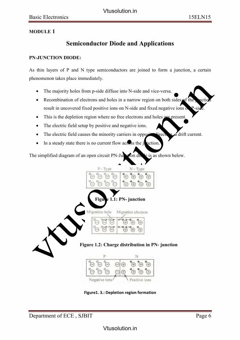
PN-JUNCTION DIODE:
As thin layers of P and N type semiconductors are joined to form a junction, a certain
phenomenon takes place immediately.
The majority holes from p-side diffuse into N-side and vice-versa.
Recombination of electrons and holes in a narrow region on both sides of the junction
result in uncovered fixed positive ions on N-side and fixed negative ions on P-side.
This is the depletion region where no free electrons and holes are present.
The electric field setup by positive and negative ions.
The electric field causes the minority carriers in opposite direction, a drift current.
In a steady state there is no current flow across the junction.
The simplified diagram of an open circuit PN-Junction diode is as shown below.
Figure 1.1: PN- junction
Figure 1.2: Charge distribution in PN- junction
Figure1. 3.: Depletion region formation
Vtusolution.in
Vtusolution.in
vtusol
ution
.in
Basic Electronics 15ELN15
Department of ECE , SJBIT Page 7
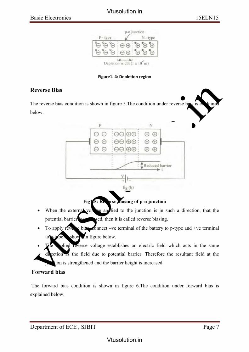
Figure1. 4: Depletion region
Reverse Bias
The reverse bias condition is shown in figure 5.The condition under reverse bias is explained
below.
Fig1.5: Reverse biasing of p-n junction
When the external voltage applied to the junction is in such a direction, that the
potential barrier is increased, then it is called reverse biasing.
To apply reverse bias, connect –ve terminal of the battery to p-type and +ve terminal
to n-type as shown in figure below.
The applied reverse voltage establishes an electric field which acts in the same
direction as the field due to potential barrier. Therefore the resultant field at the
junction is strengthened and the barrier height is increased.
Forward bias
The forward bias condition is shown in figure 6.The condition under forward bias is
explained below.
Vtusolution.in
Vtusolution.in

vtusol
ution
.in
Basic Electronics 15ELN15
Department of ECE , SJBIT Page 8
Fig1.6: Forward biasing of p-n junction
When an external voltage is applied to the junction, is in such a direction that it
cancels the potential barrier, thus permitting current flow, is called forward biasing
To apply forward bias, connect +ve terminal of the battery to p-type and –ve terminal
to n-type as shown in fig.2.1 below.
The applied forward potential establishes the electric field which acts against the field
due to potential barrier. Therefore the resultant field is weakened and the barrier
height is reduced at the junction as shown in fig.
Since the potential barrier voltage is very small, a small forward voltage is sufficient
to completely eliminate the barrier. Once the potential barrier is eliminated by the
forward voltage, junction resistance becomes almost zero and a low resistance path is
established for the entire circuit. Therefore current flows in the circuit. This is called
forward current.
Diode Relationship
The current in a diode is given by the diode current equation
I = I0( e V/ηVT –1)
Where,
I------ diode current
I0------ reverse saturation current
V------ diode voltage
η------- semiconductor constan=1 for Ge, 2 for Si.
VT------ Voltage equivalent of temperature= T/11,600 (Temperature T is in Kelvin)
Vtusolution.in
Vtusolution.in

vtusol
ution
.in
Basic Electronics 15ELN15
Department of ECE , SJBIT Page 9
Note: - If the temperature is given in 0C then it can be converted to Kelvin by the help of
following relation, 0C+273 = K
Equivalent Circuit of Diode
Ideal Diode
Fig.17a : Piecewise Linear Model
Piecewise Linear Model
When the forward characteristic of a diode is not available. A traight-line approximation,
called the piecewise linear characteristic, may be employed. To construct the piecewise linear
characteristic, VF is first. Marked on the horizontal axis, as shown in Fig1.13. Then, starting
at VF, a straight line is drawn with a slope equal to the diode dynamic resistance.
Fig1.7c : Piecewise Linear Model
Fig1.7b : Piecewise Linear Characteristic of a diode
Dynamic Resistance
rd=dVD/dID (average)
Vtusolution.in
Vtusolution.in

vtusol
ution
.in
Basic Electronics 15ELN15
Department of ECE , SJBIT Page 10
Zener diode The zener diode is a pn-junction silicon diode which is heavily doped and designed to
operate under reverse bias condition, these diodes for their operation depends on the
reverse breakdown. When once the diode breaks down the voltage across the diode
remains constant, converting the excess voltage into current and thus maintaining the
voltage across it constant, hence these diodes are very useful as voltage reference or
constant voltage devices.
Fig 1.8 : Zener diode symbol
Diodes designed to operate under reverse breakdown are found to be extremely stable over
wide range of current levels, but maintaining voltage across the device constant. The popular
voltage range for use in electronic circuits is from 2.4V to 15V, with currents less than
100mA.The desired amount of zener breakdown VZ can be achieved by controlling the
doping during the manufacture of diodes.
The zener diode when operated under forward bias has the characteristics similar to ordinary
diodes. In the zener diode symbol the direction of the arrow continues to indicate the
conventional current direction under forward bias condition.
Rectification:
“Rectifiers are the circuit which converts ac to dc”
Rectifiers are grouped into two categories depending on the period of conductions.
1. Half-wave rectifier.
2. Full- wave rectifier.
Vtusolution.in
Vtusolution.in
vtusol
ution
.in
Basic Electronics 15ELN15
Department of ECE , SJBIT Page 11
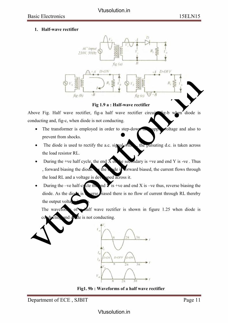
1. Half-wave rectifier
Fig 1.9 a : Half-wave rectifier
Above Fig. Half wave rectifier, fig-a half wave rectifier circuit, fig-b when diode is
conducting and, fig-c, when diode is not conducting.
The transformer is employed in order to step-down the supply voltage and also to
prevent from shocks.
The diode is used to rectify the a.c. signal while , the pulsating d.c. is taken across
the load resistor RL.
During the +ve half cycle, the end X of the secondary is +ve and end Y is -ve . Thus
, forward biasing the diode. As the diode is forward biased, the current flows through
the load RL and a voltage is developed across it.
During the –ve half-cycle the end Y is +ve and end X is –ve thus, reverse biasing the
diode. As the diode is reverse biased there is no flow of current through RL thereby
the output voltage is zero.
The waveforms of a half wave rectifier is shown in figure 1.25 when diode is
conducting and diode is not conducting.
Fig1. 9b : Waveforms of a half wave rectifier
Vtusolution.in
Vtusolution.in

vtusol
ution
.in
Basic Electronics 15ELN15
Department of ECE , SJBIT Page 12
Power conversion efficiency
It is defined as
Assuming the diode to be ideal in a HWR,
dc output = I2dcRL
ac input = I2rmsRL
√
√
(
)
η = 0.405 or 40.5% (ideal)
2. Full-wave rectifier
Full-wave rectifier is of two types
1. Centre tapped full-wave rectifier
2. Bridge rectifier
1. Centre tapped full-wave rectifier
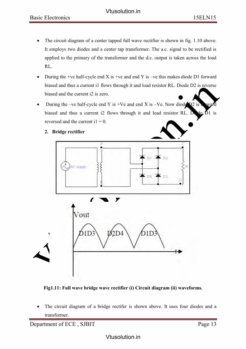
Fig1. 10: Centre tapped full-wave rectifier
Vtusolution.in
Vtusolution.in
vtusol
ution
.in
Basic Electronics 15ELN15
Department of ECE , SJBIT Page 13
The circuit diagram of a center tapped full wave rectifier is shown in fig. 1.10 above.
It employs two diodes and a center tap transformer. The a.c. signal to be rectified is
applied to the primary of the transformer and the d.c. output is taken across the load
RL.
During the +ve half-cycle end X is +ve and end Y is –ve this makes diode D1 forward
biased and thus a current i1 flows through it and load resistor RL. Diode D2 is reverse
biased and the current i2 is zero.
During the –ve half-cycle end Y is +Ve and end X is –Ve. Now diode D2 is forward
biased and thus a current i2 flows through it and load resistor RL. Diode D1 is
reversed and the current i1 = 0.
2. Bridge rectifier
Fig1.11: Full wave bridge wave rectifier (i) Circuit diagram (ii) waveforms.
The circuit diagram of a bridge rectifer is shown above. It uses four diodes and a
transformer.
Vtusolution.in
Vtusolution.in
vtusol
ution
.in
Basic Electronics 15ELN15
Department of ECE , SJBIT Page 14
During the +ve half-cycle, end A is +ve and end B is –ve thus diodes D1 and D3 are
forward bias while diodes D2 and D4 are reverse biased thus a current flows through
diode D1, load RL ( C to D) and diode D3.
During the –ve half-cycle, end B is +ve and end A is –ve thus diodes D2 and D4 are
forward biased while the diodes D1 and D3 are reverse biased. Now the flow of
current is through diode D4 load RL ( D to C) and diode D2. Thus, the waveform is
same as in the case of center-tapped full wave rectifier
Vtusolution.in
Vtusolution.in

vtusol
ution
.in
Basic Electronics 15ELN15
Department of ECE , SJBIT Page 15
BIPOLAR JUNCTION TRANSISTOR
BJT Construction and Operation:
A transistor is a sandwich of one type of semiconductor (P-type or n-type) between two
layers of other types.
Transistors are classified into two types;
1. pnp transistor
pnp transistor is obtained when a n-type layer of silicon is sandwiched between two p-type
silicon material.
2. npn transisitor
npn transistor is obtained when a p-type layer of silicon is sandwiched between two n-type
silicon materials.
Figure1.12 below shows the schematic representations of a transistor which is equivalent of
two diodes connected back to back.
Fig 1.12: Symbolic representation
Fig 1.13: Transistor symbols
The three portions of transistors are named as emitter, base and collector. The
junction between emitter and base is called emitter-base junction while the junction
between the collector and base is called collector-base junction.
Vtusolution.in
Vtusolution.in
vtusol
ution
.in
Basic Electronics 15ELN15
Department of ECE , SJBIT Page 16
The base is thin and tightly doped, the emitter is heavily doped and it is wider when
compared to base, the width of the collector is more when compared to both base and
emitter.
In order to distinguish the emitter and collector an arrow is included in the emitter.
The direction of the arrow depends on the conventional flow of current when emitter
base junction is forward biased.
In a pnp transistor when the emitter junction is forward biased the flow of current is
from emitter to base hence, the arrow in the emitter of pnp points towards the base.
Operating regions of a transistor A transistor can be operated in three different regions as
a) active region
b) saturation region
c) cut-off region
Vtusolution.in
Vtusolution.in

vtusol
ution
.in
Basic Electronics 15ELN15
Department of ECE , SJBIT Page 17
Active region
Fig1.14a: pnp transistor operated in active region
The transistor is said to be operated in active region when the emitter-base junction is
forward biased and collector –base junction is reverse biased. The collector current is
said to have two current components one is due to the forward biasing of EB junction
and the other is due to reverse biasing of CB junction. The collector current
component due to the reverse biasing of the collector junction is called reverse
saturation current (ICO or ICBO) and it is very small in magnitude.
Saturation region
Fig 1.14b: pnp transistor operated in Saturation region
Transistor is said to be operated in saturation region when both EB junction and CB junction are
forward biased as shown. When transistor is operated in saturation region IC increases rapidly for
a very small change in VC.
Vtusolution.in
Vtusolution.in

vtusol
ution
.in
Basic Electronics 15ELN15
Department of ECE , SJBIT Page 18
Cut-off region
Fig1.14c: pnp transistor operated in Cut-off region
When both EB junction and CB junction are reverse biased, the transistor is said to be
operated in cut-off region. In this region, the current in the transistor is very small and thus
when a transistor in this region it is assumed to be in off state.
Working of a transistor (pnp)
Fig1.15 Transistor in active region
Consider a pnp transistor operated in active region as shown in Figure 1.15
Since the EB junction is forward biased large number of holes present in the emitter as
majority carriers are repelled by the +ve potential of the supply voltage VEB and they
move towards the base region causing emitter current IE.
Since the base is thin and lightly doped very few of the holes coming from the emitter
recombine with the electrons causing base current IB and all the remaining holes move
towards the collector. Since the CB junction is reverse biased all the holes are
immediately attracted by the –ve potential of the supply VCB. Thereby giving rise to
collector current IC.
Vtusolution.in
Vtusolution.in

vtusol
ution
.in
Basic Electronics 15ELN15
Department of ECE , SJBIT Page 19
Thus we see that IE = IB + IC -----------------(1) (By KVL)
Since the CB junction is reverse biased a small minority carrier current ICO flows from
base to collector.
Current components of a transistor
Fig1.16: Current components of a transistor
Fig 1.16 above shows a transistor operated in active region. It can be noted from the
diagram the battery VEB forward biases the EB junction while the battery VCB reverse
biases the CB junction.
As the EB junction is forward biased the holes from emitter region flow towards the base
causing a hole current IPE. At the same time, the electrons from base region flow towards the
emitter causing an electron current INE. Sum of these two currents constitute an emitter
current IE = IPE +INE.
The ratio of hole current IPE to electron current INE is directly proportional to the ratio of the
conductivity of the p-type material to that of n-type material. Since, emitter is highly doped
when compared to base; the emitter current consists almost entirely of holes.
Not all the holes, crossing EB junction reach the CB junction because some of the them
combine with the electrons in the n-type base. If IPC is the hole current at (Jc) CB junction.
There will be a recombination current IPE - IPC leaving the base as shown in figure.
If emitter is open circuited, no charge carriers are injected from emitter into the base and
hence emitter current IE =o. Under this condition CB junction acts a a reverse biased diode
and therefore the collector current ( IC = ICO) will be equal to te reverse saturation current.
Therefore when EB junction is forward biased and collector base junction is reverse biased
the total collector current IC = IPC +ICO.
Vtusolution.in
Vtusolution.in

vtusol
ution
.in
Basic Electronics 15ELN15
Department of ECE , SJBIT Page 20
Transistor configuration
We know that, transistor can be used as an amplifier. For an amplifier, two terminals are
required to supply the weak signal and two terminals to collect the amplified signal. Thus
four terminals are required but a transistor is said to have only three terminals Therefore, one
terminal is used common for both input and output.
This gives rise to three different combinations.
1. Common base configuration (CB)
2. Common emitter configuration (CE)
3. Common collector configuration (CC)
Vtusolution.in
Vtusolution.in

vtusol
ution
.in
Basic Electronics 15ELN15
Department of ECE , SJBIT Page 21
1. CB configuration
A simple circuit arrangement of CB configuration for pnp transistor is shown below.
Fig1. 17:CB configuration
In this configuration, base is used as common to both input and output. It can be noted that
the i/p section has an a.c. source Vi along with the d.c. source VEB. The purpose of including
VEB is to keep EB junction always forward biased (because if there is no VEB then the EB
junction is forward biased only during the +ve half-cycle of the i/p and reverse biased during
the –ve half cycle). In CB configuration, IE –i/p current, IC –o/p current.
Current relations
1.current amplification factor (α)
It is defined as the ratio of d.c. collector current to d.c. emitter current
2. Total o/p current
We know that CB junction is reverse biased and because of minority charge carriers a small
reverse saturation current ICO flows from base to collector.
Since a portion of emitter current IE flows through the base ,let remaining emitter current be
αIE
Characteristics 1. Input characteristics
Vtusolution.in
Vtusolution.in

vtusol
ution
.in
Basic Electronics 15ELN15
Department of ECE , SJBIT Page 22
Fig 1.18: Input characteristics
I/p characteristics is a curve between IE and emitter base voltage VEB keeping VCB
constant. IE is taken along y-axis and VEB is taken along x-axis. From the graph following
points can be noted.
1. For small changes of VEB there will be a large change in IE. Therefore input resistance is
very small.
2. IE is almost independent of VCB
3. I/P resistance , Ri = ΔVEB / Δ IE VCB =constant
Vtusolution.in
Vtusolution.in

vtusol
ution
.in
Basic Electronics 15ELN15
Department of ECE , SJBIT Page 23
2. Output characteristics
Fig 1.19 :Output characteristics
o/p characteristics is the curve between IC and VCB at constant IE. The collector current IC
is taken along y-axis and VCB is taken along x-axis. It is clear from the graph that the o/p
current IC remains almost constant even when the voltage VCB is increased.
i.e. , a very large change in VCB produces a small change in IC. Therefore, output resistance
is very high.
O/p resistance Ro = ΔVEB / Δ IC IE = constant
Region below the curve IE =0 is known as cut-off region where IC is nearly zero. The region
to the left of VCB =0 is known as saturation region and to the right of VCB =0 is known as
active region.
2. CE configuration
Fig 1.20 :CE configuration
Vtusolution.in
Vtusolution.in

vtusol
ution
.in
Basic Electronics 15ELN15
Department of ECE , SJBIT Page 24
In this configuration the input is connected between the base and emitter while the output is
taken between collector and emitter. For this configuration IB is input current and IC is the
output current.
1. Current amplification factor (β)
It is the ratio of d.c. collector current to d.c. base current. i.e., β = IC / IB
2. Relationship between α and β
We know that α = E
C
I
I
α = CB
C
II
I
divide both numerator and denominator of RHS by IC, we get
1
1
C
B
I
I
Vtusolution.in
Vtusolution.in

vtusol
ution
.in
Basic Electronics 15ELN15
Department of ECE , SJBIT Page 25
Derivation of Total output current IC
We have CBOEC III
1)1(
1
CBOEC
CBOEC
III
IIB
I
Ic = CBOB II )1(
Transistor Characteristics
1. i/p characteristics
Fig 1.21: i/p characteristics
Input characteristics is a curve between EB voltage (VEB ) and base current (IB ) at constant
VCE. From the graph following can be noted.
1. The input characteristic resembles the forward characteristics of a p-n junction diode.
2. For small changes of VEB there will be a large change in base current IB. i.e., input
resistance is very small.
3. The base current is almost independent of VCE.
4. Input resistance , Ri = ΔVEB / Δ IB V CE = constant
Vtusolution.in
Vtusolution.in

vtusol
ution
.in
Basic Electronics 15ELN15
Department of ECE , SJBIT Page 26
2. Output characteristics
Fig1. 22: Output characteristics
It is the curve between VCE and IC at constant IB. From the graph we can see that,
1. Very large changes of VCE produces a small change in IC i.e output resistance is very
high.
2. output resistance Ro = ΔVCE / ΔIC IB = constant
Region between the curve IB =0 is called cut-off region where IB is nearly zero. Similarly the
active region and saturation region is shown on the graph.
Vtusolution.in
Vtusolution.in

vtusol
ution
.in
Basic Electronics 15ELN15
Department of ECE , SJBIT Page 27
Recommended questions 1. Explain the VI- characteristics of a pn-junction diode.
2. Sketch the typical V-I characteristics of PN junction diode and identify the important
points.
3. Draw and explain the V-I characteristics of Si and Ge diodes.
4. Derive an expression for the ripple factor and efficiency of half wave rectifier (HWR).
5. Explain the quantitative theory of p-n junction.
6. With the help of the diode equation, explain the V-I characteristics of p-n junction
7. Explain the V-I characteristics with respect to the current equation
8. Draw and explain V-I characteristics of p-n junction diode
9. Write the current equation of a p-n junction and explain the V-I characteristics. What
is the effect of temperature on cut-in voltage and reverse saturation current?
10. Differentiate between Zener breakdown and Avalanche breakdown.
11. Draw and explain V-I characteristics of a p-n junction diode .
12. Explain the working of NPN transistor.
13. Draw a sketch to show the various current components in a transistor. Briefly explain
the origin of each current.
14. Draw and explain the input and output characteristics of a transistor in CE
configuration.
15. Transistor means “Transfer Resistance”. Discuss.
16. Write the circuit of Common Base configuration and explain its output
characteristics.
17. Define α dc and β dc of a transistor. Obtain relationship between them.
18. Explain the concept of dc load line and ac load line of a CE amplifier.
Vtusolution.in
Vtusolution.in

vtusol
ution
.in
Basic Electronics 15ELN15
Department of ECE , SJBIT Page 28
MODULE 2
BJT BIASING Transistor biasing is the establishment of suitable dc values such as Ic, VCE, IB etc. by using
a single dc source... When BJT is properly biased, faithful amplification of signals take place.
For example applying forward bias to EB- junction and reverse bias to the CB-junction
makes the transistor to operate in the active region. Hence Biasing is applying dc voltages to
the junctions of the transistor to make it operate in the desired region. Biasing eliminates the
need for separate dc sources in the emitter and collector circuits.
Types of biasing.
There are mainly three types of biasing circuits used for biasing a transistor, they are:
a) Base bias or fixed bias
b) Collector to base bias
c) Voltage divider bias
The three biasing circuits are shown in figure 1.23
Fig 2.1 : The three basic biasing circuits.
a) Base bias or fixed bias:
For this configuration the biasing arrangement is as shown in figure1.24 below. A base
resistance RB is used between Vcc and base to establish the base current IB Thus the base
current is the constant quantity determined by Vcc and IB. Because Vcc and RB are fixed
quantities, IB remains fixed and hence it is also called fixed bias.
Vtusolution.in
Vtusolution.in

vtusol
ution
.in
Basic Electronics 15ELN15
Department of ECE , SJBIT Page 29
Fig 2.2: Base bias circuit.
Applyingh Kirchoff„s voltage law to the base circuirt. (The base circuit consists of Vcc,
RB,EB- junction of the transistor and ground)
IB RB +VBE=Vcc
IB =(Vcc- VBE)/ RB
VBE is 0.7V for Silicon and 0.3V for Germanium transistor.
The collector current is calculated as
Ic= β IB.
Applying the KVL to collector circuit (The collector circuit consists of Vcc, Rc, VCE, and
ground
Vcc= VCE +IcRc
VCE =Vcc –IcRc
Voltage divider bias circuit
Circuit operation
Voltage divider bias also known as emitter current bias, is the most stable of the three basic
transistor biasing circuits. A voltage divider bias circuit is shown in fig. below, and the
current and voltage conditions throughout the discussions are illustrated in fig.8. It is seen
that there is an emitter resistor RE connected in series with emitter, so that the total dc load in
series with the transistor is (Rc+ RE) and this resistance must be used when drawing the dc
load line for the circuit. Resistor R1 and R2 constitute a voltage divider that divides the
supply voltage to produce the base bias voltage IB.
Voltage divider bias circuits are normally designed to have the voltage divider current (I2)
very much larger than the transistor base current (IB).In this circumstance, VBE is largely
affected by IB so VBE can be assumed to remain constant.
Vtusolution.in
Vtusolution.in
vtusol
ution
.in
Basic Electronics 15ELN15
Department of ECE , SJBIT Page 30
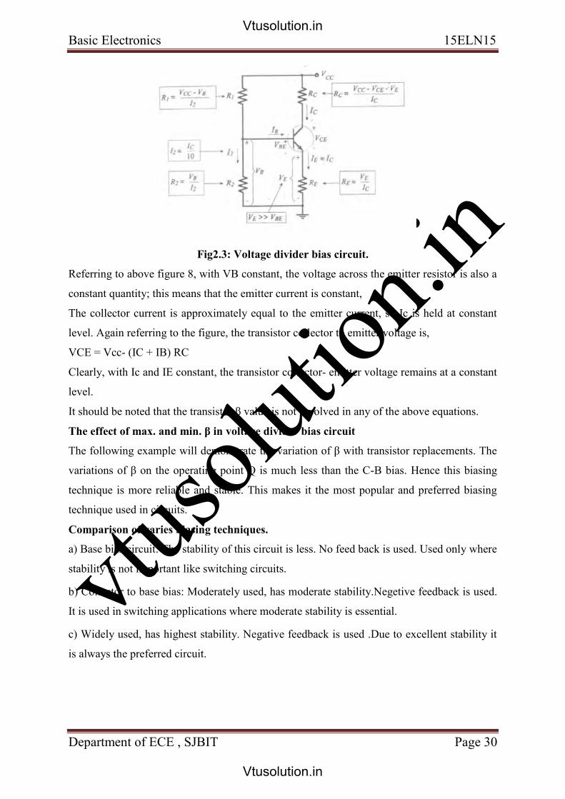
Fig2.3: Voltage divider bias circuit.
Referring to above figure 8, with VB constant, the voltage across the emitter resistor is also a
constant quantity; this means that the emitter current is constant,
The collector current is approximately equal to the emitter current, so Ic is held at constant
level. Again referring to the figure, the transistor collector to emitter voltage is,
VCE = Vcc- (IC + IB) RC
Clearly, with Ic and IE constant, the transistor collector- emitter voltage remains at a constant
level.
It should be noted that the transistor β value is not involved in any of the above equations.
The effect of max. and min. β in voltage divider bias circuit
The following example will demonstrate the variation of β with transistor replacements. The
variations of β on the operating point Q is much less than the C-B bias. Hence this biasing
technique is more reliable and stable. This makes it the most popular and preferred biasing
technique used in circuits.
Comparison of varies biasing techniques.
a) Base bias circuit: The stability of this circuit is less. No feed back is used. Used only where
stability is not important like switching circuits.
b) Collector to base bias: Moderately used, has moderate stability.Negetive feedback is used.
It is used in switching applications where moderate stability is essential.
c) Widely used, has highest stability. Negative feedback is used .Due to excellent stability it
is always the preferred circuit.
Vtusolution.in
Vtusolution.in

vtusol
ution
.in
Basic Electronics 15ELN15
Department of ECE , SJBIT Page 31
OPERATIONAL AMPLIFIER INTRODUCTION
Op-Amp (operational amplifier) is basically an amplifier available in the IC form. The word
operational is used because the amplifier can be used to perform a variety of mathematical
operations such as addition, subtraction, integration, differentiation etc.
Fig.1 below shows the symbol of an Op-Amp.
Fig2.4 Symbol of Op-Amp
It has two inputs and one output. The input marked „-„ is known as Inverting input and the
input marked „+‟ is known as Non-inverting input.
OPAMP ARCHITECTURE
Fig2.5: Block diagram of an Op-Amp
Input stage: It consists of a dual input, balanced output differential amplifier. Its function is to
amplify the difference between the two input signals. It provides high differential gain, high
input impedance and low output impedance.
Intermediate stage: The overall gain requirement of an Op-Amp is very high. Since the input
stage alone cannot provide such a high gain. Intermediate stage is used to provide the
required additional voltage gain.
It consists of another differential amplifier with dual input, and unbalanced ( single ended)
output
Vtusolution.in
Vtusolution.in

vtusol
ution
.in
Basic Electronics 15ELN15
Department of ECE , SJBIT Page 32
If a voltage Vi is applied at the inverting input ( keeping the non-inverting input at ground) as
shown below.
Fig2.6: Op-amp in inverting mode
The output voltage Vo= -AVi is amplified but is out of phase with respect to the input signal
by 1800.
If a voltage Vi is fed at the non-inverting input ( Keeping the inverting input at ground) as
shown below.
Fig2.7: Op-Amp in Non-inverting mode
The output voltage Vo= AVi is amplified and in-phase with the input signal.
If two different voltages V1 and V2 are applied to an ideal Op-Amp as shown below.
Fig2.8: Ideal Op-Amp
Vtusolution.in
Vtusolution.in

vtusol
ution
.in
Basic Electronics 15ELN15
Department of ECE , SJBIT Page 33
The output voltage will be Vo = A(V1 – V2)
i.e the difference of the tow volatages is amplified. Hence an Op-Amp is also called as a High
gain differential amplifier.
Applications of Op-Amp
An Op-Amp can be used as
1. Inverting Amplifer
2. Non-Iverting Amplifer
3. Voltage follower
4. Adder ( Summer)
5. Integrator
6. Differentiator
Definitions
Slewrate (S): It is defined as ― The rate of change of output voltage per unit time.
sec/ voltsdt
dVs O
Ideally slew rate should be as high as possible. But its typical value is s=0.5 V/μ-sec.
2. Common Mode Rejection Ratio(CMRR): It is defined as ― The ratio of differential
voltage gain to common-mode voltage gain‖.
CM
d
A
ACMRR
Ideally CMRR is infinite, but its typical value is CMRR = 90 dB
3. Open Loop Voltage Gain (AV): It is the ration of output voltage to input voltage in the
absence of feed back.
Its typical value is AV = 2x10⁵
4. Input Impedance (Ri):It is defined as ― The impedance seen by the input(source)
applied to one input terminal when the other input terminal is connected to ground.
Ri ≈ 2MΩ
5. Output Impedance (RO): It is defined as ― The impedance given by the output (load) for
a particular applied input‖.
Vtusolution.in
Vtusolution.in

vtusol
ution
.in
Basic Electronics 15ELN15
Department of ECE , SJBIT Page 34
Ro ≈ 75Ω
Inverting Amplifier
An inverting amplifier is one whose output is amplified and is out of phase by 1800 with
respect to the input.
Fig2.9: Inverting Amplifier
The point ―G‖ is called virtual ground and is equal to zero.
By KCL we have
21 ii
f
oi
R
V
R
V
00
1
f
oi
R
V
R
V
1
i
f
O VR
RV
1
Where 1R
R f the gain of the amplifier and negative sign is indicates that the output is
inverted with respect to the input.
Fig2.10: Waveforms of Inverting Amplifers
Vtusolution.in
Vtusolution.in

vtusol
ution
.in
Basic Electronics 15ELN15
Department of ECE , SJBIT Page 35
Non- Inverting Amplifier
A non-inverting amplifier is one whose output is amplified and is in-phase with the input
Fig2.11: Non Inverting Amplifiers
By KCL we have
21 ii
f
Oii
R
VV
R
V
1
0
1
0
1
R
R
V
ViV
R
VV
R
V
f
i
f
iOi
1
1R
R
V
V f
i
O
i
f
i
O
R
R
V
V1
i
fV
R
RV
10 1
Where
1
1R
R f is the gain of the amplifier and + sign indicates that the output is
in-phase with the input.
Vtusolution.in
Vtusolution.in

vtusol
ution
.in
Basic Electronics 15ELN15
Department of ECE , SJBIT Page 36
3. Voltage follower
Fig2. 12: Voltage follower
Voltage follower is one whose output is equal to the input.
The voltage follower configuration shown above is obtained by short circuiting “Rf” and
open circuiting “R1” connected in the usual non-inverting amplifier.
Thus all the output is fed back to the inverting input of the op-Amp.
Consider the equation for the output of non-inverting amplifer
i
fV
R
RV
10 1
When Rf = 0 short circuiting
R1= ∞ open circuiting
iV
01V O
iO VV
Therefore the output voltage will be equal and in-phase with the input voltage. Thus
voltage follower is nothing but a non-inverting amplifier with a voltage gain of unity.
Vtusolution.in
Vtusolution.in

vtusol
ution
.in
Basic Electronics 15ELN15
Department of ECE , SJBIT Page 37
4. Inverting Adder
Inverting adder is one whose output is the inverted sum of the constituent inputs
Fig2.13. Inverting Adder
By KCL we have
321 iiii f
3
3
2
2
1
1 0000R
V
R
V
R
V
R
V
f
O
3
3
2
2
1
1
RV
R
V
R
V
R
V
f
O
3
3
2
2
1
1
RV
R
V
R
VRV fO
If R1 = R2 = R3 =R then
321 VVVR
RV
f
O
If Rf = R then
VO = -[ V1 + V2 + V3 ]
Hence it can be observed that the output is equal to the inverted sum of the inputs.
Vtusolution.in
Vtusolution.in

vtusol
ution
.in
Basic Electronics 15ELN15
Department of ECE , SJBIT Page 38
5. Integrator
Fig2,14: Integrator
An integrator is one whose output is the integration of the input.,
By KCL we have,
121 ii
iO
Oi
O
O
O
O
ii
VRCdt
dV
dt
dVC
R
V
haveweinandgsubstituin
dt
dVCiei
iCdt
dV
dtiC
V
dtiC
V
havewesimilarlyand
R
V
R
Vi
havewefigureabovetheFrom
1
132
3..
1
1
10
20
2
2
2
2
1
Vtusolution.in
Vtusolution.in

vtusol
ution
.in
Basic Electronics 15ELN15
Department of ECE , SJBIT Page 39
dtVRC
V iO 1
Vtusolution.in
Vtusolution.in

vtusol
ution
.in
Basic Electronics 15ELN15
Department of ECE , SJBIT Page 40
6.Differentiator
A differentiator is one whose output is the differentiation of the input.
Fig2,15: Differentiator
By KCL we have
R
V
dt
dVC
haveweinandngsubstituti
R
V
R
Vi
havewesimilarlyand
dt
dVCi
iCdt
dV
dtiC
V
havewefigureabovetheFrom
ii
Oi
OO
i
i
i
132
30
2.
1
1
1
2
1
1
1
21
dt
dVRCVO
Vtusolution.in
Vtusolution.in

vtusol
ution
.in
Basic Electronics 15ELN15
Department of ECE , SJBIT Page 41
Recommended Questions
1. List of characteristics of an ideal Op-Amp
2. Explain the application of an Op-Amp as a voltage follower.
3. What is an Op-Amp? What are the basic properties of an Op-Amp
4. Explain the working of Op-Amp as Summing Amplifier
5. Explain the working of Op-Amp as Integrator
6. Explain the working of Op-Amp as Differentiator
7. Explain the working of Op-Amp as Voltage Follower
8. Explain the working of Op-Amp as Current to voltage converter.
9. Explain the working of Op-Amp as Voltage to current converter.
Vtusolution.in
Vtusolution.in

vtusol
ution
.in
Basic Electronics 15ELN15
Department of ECE , SJBIT Page 42
MODULE 3
DIGITAL ELECTRONICS
NUMBER SYSTEM
The human need to count things goes back to the dawn of civilization. To answer the
questions like ―how much‖, or ―how many‖, people invented number system. A number
system is any scheme used to count things. The decimal number system succeeded because
very large numbers can be expressed using relatively short series of easily memorized
numerals. Decimal or base 10 number system„s origin: can be traced to, counting on the
fingers with digits. ―Digit‖ taken from the Latin word digitus meaning ―finger‖
In any number system, the important terms to be known are :
Base or radix, numerals, positional value, absolute value, radix point and the prevalent
number systems of interest for study.
Base: Base is the number of different digits or symbols or numerals used to represent the
number system including zero in the number system. It is also called the radix of the number
system.
Numeral : Numeral is the symbols used to represent the number system
Each digit in the number system has two values:
a) Absolute value
b) Positional value
The absolute value is the value of the digit itself, representing the no. system. The positional
value is the value it possesses by virtue of its position in the no. system
The different number systems of interest for study, from the point of view of application to
computers are:
Examples of commonly used number systems :
1. decimal
2. binary
3. octal
4. hexadecimal.
Important properties of these systems need to be studied.
Polynomial Notation (Series Representation) :Any number system can be represented by
the following polynomial.
Vtusolution.in
Vtusolution.in

vtusol
ution
.in
Basic Electronics 15ELN15
Department of ECE , SJBIT Page 43
N = an-1 x rn-1 + an-2 x rn-2 + .. + a0 x r0 + a-1 x r-1 ... + a-m x r–m Where
r = radix or base
n = number of integer digits to the left of the radix point
m = number of fractional digits to the right of the radix point
an-1 = most significant digit (MSD)
a-m = least significant digit (LSD)
Example: N = (251.41)10 = 2 x 10² + 5 x 101 + 1 x 100 + 4 x 10⁻¹ + 1 x 10⁻²
Decimal number system :
The decimal system is composed of 10 numerals or symbols. These 10 symbols are 0, 1, 2, 3,
4, 5, 6, 7, 8, 9. Using these symbols as digits of a number, we can express any quantity. The
decimal system is also called the base-10 system because it has 10 digits.
In decimal system, the no. 1000.111 is represented as:
Example : Multiply the value of the symbol by the value of the position, then add
In decimal, 1954.89means
1 times 1,000
plus 9 times 100
plus 5 times 10
plus 4 times 1
plus 8 times 1/10
plus 9 times 1/100 = The number is 1954.89 in decimal. and is represented by (1954.89)10.
The digits are separated by a point “.” called the radix point. In decimal system it is called
―decimal point‖.
Decimal Examples of decimal numbers
1410
5210
102410
6400010
Vtusolution.in
Vtusolution.in

vtusol
ution
.in
Basic Electronics 15ELN15
Department of ECE , SJBIT Page 44
Binary number system :
In the binary system, there are only two symbols or possible digit values, 0 and 1. This base-2
system can be used to represent any quantity that can be represented in decimal or other base
system.
Vtusolution.in
Vtusolution.in

vtusol
ution
.in
Basic Electronics 15ELN15
Department of ECE , SJBIT Page 45
Binary Counting
The Binary counting sequence to represent decimal numbers is shown in the table
below
23 2
2 21 2
0 Decimal
0 0 0 0 0
0 0 0 1 1
0 0 1 0 2
0 0 1 1 3
0 1 0 0 4
0 1 0 1 5
0 1 1 0 6
0 1 1 1 7
1 0 0 0 8
1 0 0 1 9
1 0 1 0 10
1 0 1 1 11
1 1 0 0 12
1 1 0 1 13
1 1 1 0 14
1 1 1 1 15
Octal Number System
The octal number system has a base of eight, meaning that it has eight possible digits:
0,1,2,3,4,5,6,7.
83 8
2 81 8
0 8
-1 8-2 8
-3
=512 =64 =8 =1 . =1/8 =1/64 =1/512
The octal numbering system includes eight base digits (0-7).After 7, the next
placeholder to the right begins with a “1”
0, 1, 2, 3, 4, 5, 6, 7, 10, 11, 12, 13 ...
Octal to Decimal Conversion
2378 = 2 x (82) + 3 x (81) + 7 x (80) = 15910
Vtusolution.in
Vtusolution.in

vtusol
ution
.in
Basic Electronics 15ELN15
Department of ECE , SJBIT Page 46
24.68 = 2 x (81) + 4 x (80) + 6 x (8-1) = 20.7510
11.18 = 1 x (81) + 1 x (80) + 1 x (8-1) = 9.12510
12.38 = 1 x (81) + 2 x (80) + 3 x (8-1) = 10.37510
Hexadecimal number system
The hexadecimal system uses base 16. Thus, it has 16 possible digit symbols. It uses the
digits 0 through 9 plus the letters A, B, C, D, E, and F ,to represent 10 through 16, as the 16
digit symbols
Digits = 0, 1, 2, 3, 4, 5, 6, 7, 8, 9, A, B, C, D, E, F
(B65F)16 = 11 x 163 + 6 x 162 + 5 x 161 + 15 x 160 = (46,687)10
Sometimes, it is necessary to use a numbering system that has more than ten base
digits
One such numbering system is hexadecimal number system, useful in computer
application.
Hexadecimal number, is widely used in micro processors and micro controllers in
assembly programming, and in embedded system development.
Conversion of number systems.
The above diagram shows all the possibilities of conversions discussed below. However the
possibilities of conversions can be summarized in to the following three categories :
Case 1: Conversion from decimal to other number system.
Case 2: Conversion from other number system to decimal number system.
Case 3: Conversion from among number systems other than decimal number system.
1. Binary-To-Decimal Conversion
The binary number system is the most important one in digital systems, but several others are
also important. The decimal system is important because it is universally used to represent
quantities outside a digital system. This means that there will be situations where decimal
values have to be converted to binary values before they are entered into the digital system.
Vtusolution.in
Vtusolution.in

vtusol
ution
.in
Basic Electronics 15ELN15
Department of ECE , SJBIT Page 47
Any binary number can be converted to its decimal equivalent simply by summing together
the weights of the various positions in the binary number which contain a
together the weights of the various positions in the binary number which contain a 1.
Technique
Multiply each bit by 2n, where n is the “weight” of the bit
The weight is the position of the bit, starting from 0 on the right
Add the results
Binary Decimal
101101012
27+06+25+24+03+22+01+20 =128+0+32+16+0+4+0+1
Result 18110
You should have noticed that the method is to find the weights (i.e., powers of 2) for each bit
position that contains a 1, and then to add them up.
Binary to decimal Fractions:
Example :
10.1011 => 1x2-4=0.0625
1x2-3=0.125
0x2-2=0.0
1x2-1=0.5
0x20=0.0
1x21=2.0
=2.6875
Procedure: Same principles with following exception ;.
Use negative powers of the base to the right of the radix point. (Only call it a decimal point in
the decimal number system.)
2. Decimal-To-Binary Conversion
Vtusolution.in
Vtusolution.in

vtusol
ution
.in
Basic Electronics 15ELN15
Department of ECE , SJBIT Page 48
There are 2 methods:
Reverse of Binary-To-Decimal Method
Repeat Division
Reverse of Binary-To-Decimal Method
Decimal Binary
4510 =32 + 0 + 8 + 4 +0 + 1
=25+0+23+22+0+20
Result =1011012
Repeat Division-Convert decimal to binary
This method uses repeated division by 2.
Example : Conversion of 2710 to binary
Division Remainder Binary
25/2 = 12+ remainder of 1 1 (Least Significant Bit)
12/2 = 6 + remainder of 0 0
6/2 = 3 + remainder of 0 0
3/2 = 1 + remainder of 1 1
1/2 = 0 + remainder of 1 1 (Most Significant Bit)
Result 2510 = 110012
3. Binary-To-Octal / Octal-To-Binary Conversion
Octal Digit 0 1 2 3 4 5 6 7
Binary Equivalent 000 001 010 011 100 101 110 111
Each Octal digit is represented by three binary digits.
Example: 100 111 0102 = (100) (111) (010)2 = 4 7 28
4. Octal to decimal
Vtusolution.in
Vtusolution.in

vtusol
ution
.in
Basic Electronics 15ELN15
Department of ECE , SJBIT Page 49
Procedure
Multiply each bit by 8n, where n is the “weight” of the bit
The weight is the position of the bit, starting from 0 on the right
Add the results.
Example:
724.258 => 4x80=4
2x81=16
7 x 82 = 448
2 x 1/8 = 0.25
5x1/82=0.015625
Ans: 7248 =468.26562510
Vtusolution.in
Vtusolution.in

vtusol
ution
.in
Basic Electronics 15ELN15
Department of ECE , SJBIT Page 50
5. Hexadecimal to Decimal/Decimal to Hexadecimal Conversion
Example: 2AF16 = 2 x (162) + 10 x (161) + 15 x (160) = 68710
5.1 Hexadecimal to Decimal Conversion
Technique
Multiply each bit by 16n, where n is the “weight” of the bit
The weight is the position of the bit, starting from 0 on the right
Add the results
Example:
ABC.6D16 => Cx160=12x1=12
Bx161=11x16=176
A x 162 = 10 x 256 = 2560
6 x 1/16 = 6 x .0625
D x 1/162 = 13 x .0039
= 2748.066410
Ans: ABC16 = 2748.066410
24.616 = 2 x (161) + 4 x (160) + 6 x (16-1) = 36.37510
11.116 = 1 x (161) + 1 x (160) + 1 x (16-1) = 17.062510
12.316 = 1 x (161) + 2 x (160) + 3 x (16-1) = 18.187510
Vtusolution.in
Vtusolution.in
vtusol
ution
.in
Basic Electronics 15ELN15
Department of ECE , SJBIT Page 51
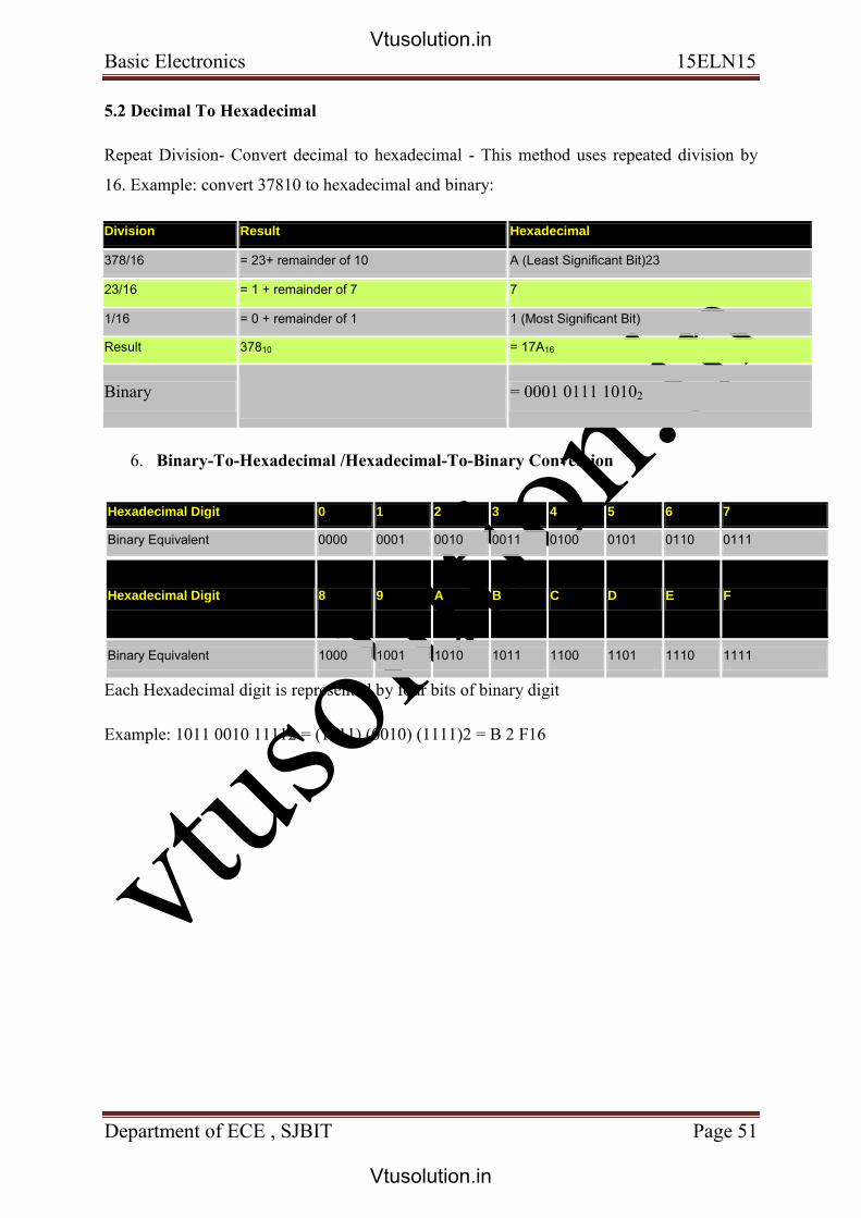
5.2 Decimal To Hexadecimal
Repeat Division- Convert decimal to hexadecimal - This method uses repeated division by
16. Example: convert 37810 to hexadecimal and binary:
Division Result Hexadecimal
378/16 = 23+ remainder of 10 A (Least Significant Bit)23
23/16 = 1 + remainder of 7 7
1/16 = 0 + remainder of 1 1 (Most Significant Bit)
Result 37810 = 17A16
Binary = 0001 0111 10102
6. Binary-To-Hexadecimal /Hexadecimal-To-Binary Conversion
Hexadecimal Digit 0 1 2 3 4 5 6 7
Binary Equivalent 0000 0001 0010 0011 0100 0101 0110 0111
Hexadecimal Digit 8 9 A B C D E F
Binary Equivalent 1000 1001 1010 1011 1100 1101 1110 1111
Each Hexadecimal digit is represented by four bits of binary digit
Example: 1011 0010 11112 = (1011) (0010) (1111)2 = B 2 F16
Vtusolution.in
Vtusolution.in

vtusol
ution
.in
Basic Electronics 15ELN15
Department of ECE , SJBIT Page 52
Complement of Binary no. system
The 1‟s complement of a given binary no. is the new no. obtained by changing all the 0‟ to 1,
and all 0‟s to 1
Ex : 11010‟s 1‟s complement is 00101 The 2‟s complement of a given binary no. is the new no. obtained by changing all the 0‟ to 1,
and all 0‟s to 1 and then adding 1 to the least significant it
Ex : 11010‟s 2‟s complement is 1‟s complement 00101+1=00110
Vtusolution.in
Vtusolution.in

vtusol
ution
.in
Basic Electronics 15ELN15
Department of ECE , SJBIT Page 53
BOOLEAN ALGEBRA THEOREMS:
Identity :- X + 0 = X, X . 1 = X
Commutative Laws : X + Y = Y + X, X . Y = Y . X
Distributive Laws : X.(Y + Z ) = X.Y + X.Z, X + Y.Z = (X + Y) . (X + Z)
Complement : X + X' = 1, X . X' = 0,
The complement X' is unique.
Idempotent Law : X + X = X, X . X = X
Vtusolution.in
Vtusolution.in

vtusol
ution
.in
Basic Electronics 15ELN15
Department of ECE , SJBIT Page 54
DeMorgan's Law:
(X + Y)' = X' . Y', These can be proved by the use of truth tables.
Proof of (X + Y)' = X' . Y'
X Y X+Y (X+Y)'
0 0 0 1
0 1 1 0
1 0 1 0
1 1 1 0
X Y X' Y' X'.Y'
0 0 1 1 1
0 1 1 0 0
1 0 0 1 0
1 1 0 0 0
The two truth tables are identical, and so the two expressions are identical
(X.Y) = X' + Y', These can be proved by the use of truth tables
Proof of (X.Y) = X' + Y'
X Y X.Y (X.Y)'
0 0 0 1
0 1 0 1
1 0 0 1
X Y X' Y' X'+Y'
0 0 1 1 1
0 1 1 0 1
1 0 0 1 1
1 1 0 0 0
Vtusolution.in
Vtusolution.in

vtusol
ution
.in
Basic Electronics 15ELN15
Department of ECE , SJBIT Page 55
Logic Gates
A logic gate is an electronic circuit/device which makes the logical decisions. To arrive at
this decisions, the most common logic gates used are OR, AND, NOT, NAND, and NOR
gates. The NAND and NOR gates are called universal gates. The exclusive-OR gate is
another logic gate which can be constructed using AND, OR and NOT gate.
Logic gates have one or more inputs and only one output. The output is active only for certain
input combinations. Logic gates are the building blocks of any digital circuit. Logic gates are
also called switches. With the advent of integrated circuits, switches have been replaced by
TTL (Transistor Transistor Logic) circuits and CMOS circuits. Here I give example circuits
on how to construct simples gates.
Truth Tables
Truth tables are a means of representing the results of a logic function using a table. They are
constructed by defining all possible combinations of the inputs to a function, and then
calculating the output for each combination in turn. For the three functions we have just
defined, the truth tables are as follows.
Symbolic Logic
Boolean algebra derives its name from the mathematician George Boole. Symbolic Logic
uses values, variables and operations.
Inversion
A small circle on an input or an output indicates inversion. See the NOT, NAND and NOR
gates given below for examples.
Multiple Input Gates
Vtusolution.in
Vtusolution.in
vtusol
ution
.in
Basic Electronics 15ELN15
Department of ECE , SJBIT Page 56
Given commutative and associative laws, many logic gates can be implemented with more
than two inputs, and for reasons of space in circuits, usually multiple input, complex gates are
made. You will encounter such gates in real world (maybe you could analyze an ASIC lib to
find this).
Gates Types
AND
OR
NOT
NAND
NOR
XOR
XNOR
1. AND Gate
The AND gate performs logical multiplication, commonly known as AND function. The
AND gate has two or more inputs and single output. The output of AND gate is HIGH only
when all its inputs are HIGH (i.e. even if one input is LOW, Output will be LOW).
If X and Y are two inputs, then output F can be represented mathematically as F = X.Y, Here
dot (.) denotes the AND operation. Truth table and symbol of the AND gate is shown in the
figure below.
Vtusolution.in
Vtusolution.in

vtusol
ution
.in
Basic Electronics 15ELN15
Department of ECE , SJBIT Page 57
Symbol
Truth Table
X Y F=(X.Y)
0 0 0
0 1 0
1 0 0
1 1 1
2. OR Gate
The OR gate performs logical addition, commonly known as OR function. The OR gate has
two or more inputs and single output. The output of OR gate is HIGH only when any one of
its inputs are HIGH (i.e. even if one input is HIGH, Output will be HIGH)
If X and Y are two inputs, then output F can be represented mathematically as F = X+Y. Here
plus sign (+) denotes the OR operation. Truth table and symbol of the OR gate is shown in
the figure below.
Symbol
Vtusolution.in
Vtusolution.in

vtusol
ution
.in
Basic Electronics 15ELN15
Department of ECE , SJBIT Page 58
Truth Table
X Y F=(X+Y)
0 0 0
0 1 1
1 0 1
1 1 1
3. NOT Gate
The NOT gate performs the basic logical function called inversion or complementation. NOT
gate is also called inverter. The purpose of this gate is to convert one logic level into the
opposite logic level. It has one input and one output. When a HIGH level is applied to an
inverter, a LOW level appears on its output and vice versa.
If X is the input, then output F can be represented mathematically as F = X', Here apostrophe
(') denotes the NOT (inversion) operation. There are a couple of other ways to represent
inversion, F= !X, here ! represents inversion. Truth table and NOT gate symbol is shown in
the figure below
Symbol
Truth Table
X Y=X'
0 1
1 0
NOT gate using "transistor-resistor" logic is shown in the figure below, where X is the input
and F is the output Circuit
Vtusolution.in
Vtusolution.in

vtusol
ution
.in
Basic Electronics 15ELN15
Department of ECE , SJBIT Page 59
4. NAND Gate
NAND gate is a cascade of AND gate and NOT gate, as shown in the figure below. It has two
or more inputs and only one output. The output of NAND gate is HIGH when any one of its
input is LOW (i.e. even if one input is LOW, Output will be HIGH).
NAND From AND and NOT
If X and Y are two inputs, then output F can be represented mathematically as F = (X.Y)',
Here dot (.) denotes the AND operation and (') denotes inversion. Truth table and symbol of
the N AND gate is shown in the figure below. Symbol
Truth Table
X Y F=(X.Y)'
0 0 1
0 1 1
1 0 1
1 1 0
5. NOR Gate
NOR gate is a cascade of OR gate and NOT gate, as shown in the figure below. It has two or
more inputs and only one output. The output of NOR gate is HIGH when any all its inputs are
LOW (i.e. even if one input is HIGH, output will be LOW)
Vtusolution.in
Vtusolution.in

vtusol
ution
.in
Basic Electronics 15ELN15
Department of ECE , SJBIT Page 60
Symbol
If X and Y are two inputs, then output F can be represented mathematically as F = (X+Y)';
here plus (+) denotes the OR operation and (') denotes inversion. Truth table and symbol of
the NOR gate is shown in the figure below.
Truth Table
X Y F=(X+Y)'
0 0 1
0 1 0
1 0 0
1 1 0
6. XOR Gate
An Exclusive-OR (XOR) gate is gate with two or three or more inputs and one output. The
output of a two-input XOR gate assumes a HIGH state if one and only one input assumes a
HIGH state. This is equivalent to saying that the output is HIGH if either input X or input Y
is HIGH exclusively, and LOW when both are 1 or 0 simultaneously
If X and Y are two inputs, then output F can be represented mathematically as F = X Y,
Here denotes the XOR operation. X Y and is equivalent to X.Y' + X'.Y. Truth table and
symbol of the XOR gate is shown in the figure below
XOR From Simple gates
Vtusolution.in
Vtusolution.in

vtusol
ution
.in
Basic Electronics 15ELN15
Department of ECE , SJBIT Page 61
Symbol
Truth Tabl
X Y F=(X Y)
0 0 0
0 1 1
1 0 1
1 1 0
7. XNOR Gate
An Exclusive-NOR (XNOR) gate is gate with two or three or more inputs and one output. The
output of a two-input XNOR gate assumes a HIGH state if all the inputs assumes same state.
This is equivalent to saying that the output is HIGH if both input X and input Y is HIGH
exclusively or same as input X and input Y is LOW exclusively, and LOW when both are not
same. If X and Y are two inputs, then output F can be represented mathematically as F = X
Y, Here denotes the XNOR operation. X Y and is equivalent to X.Y + X'.Y'. Truth table
and symbol of the XNOR gate is shown in the figure below.
Symbol
Truth Table
X Y F=(X Y)'
0 0 1
0 1 0
1 0 0
1 1 1
Vtusolution.in
Vtusolution.in

vtusol
ution
.in
Basic Electronics 15ELN15
Department of ECE , SJBIT Page 62
Universal Gates
Universal gates are the ones which can be used for implementing any gate like AND, OR and
NOT, or any combination of these basic gates; NAND and NOR gates are universal gates.
But there are some rules that need to be followed when implementing NAND or NOR based
gate
To facilitate the conversion to NAND and NOR logic, we have two new graphic symbols for
these gates
1. NAND Gate
2. NOR Gate
Realization of logic function using NAND gates
Any logic function can be implemented using NAND gates. To achieve this, first the logic
function has to be written in Sum of Product (SOP) form. Once logic function is converted to
SOP, then is very easy to implement using NAND gate. In other words any logic circuit with
AND gates in first level and OR gates in second level can be converted into a NAND-NAND
gate circuit.
Realization of logic gates using NAND gates
Vtusolution.in
Vtusolution.in
vtusol
ution
.in
Basic Electronics 15ELN15
Department of ECE , SJBIT Page 63
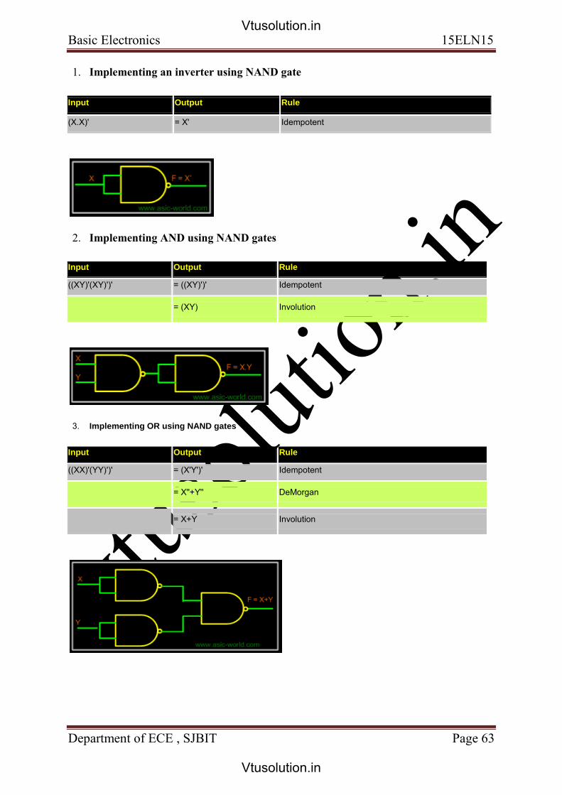
1. Implementing an inverter using NAND gate
Input Output Rule
(X.X)' = X' Idempotent
2. Implementing AND using NAND gates
Input Output Rule
((XY)'(XY)')' = ((XY)')' Idempotent
= (XY) Involution
3. Implementing OR using NAND gates
Input Output Rule
((XX)'(YY)')' = (X'Y')' Idempotent
= X''+Y'' DeMorgan
= X+Y Involution
Vtusolution.in
Vtusolution.in

vtusol
ution
.in
Basic Electronics 15ELN15
Department of ECE , SJBIT Page 64
4. Implementing NOR using NAND gates
Input Output Rule
((XX)'(YY)')' =(X'Y')' Idempotent
=X''+Y'' DeMorgan
=X+Y Involution
=(X+Y)' Idempotent
Realization of logic function using NOR gates
Any logic function can be implemented using NOR gates. To achieve this, first the logic
function has to be written in Product of Sum (POS) form. Once it is converted to POS, then
it's very easy to implement using NOR gate. In other words any logic circuit with OR gates in
first level and AND gates in second level can be converted into a NOR-NOR gate circuit.
1. Implementing an inverter using NOR gate
Input Output Rule
(X+X)' = X' Idempotent
2. Implementing AND using NOR gates
Input Output Rule
((X+X)'+(Y+Y)')' =(X'+Y')' Idempotent
= X''.Y'' DeMorgan
Vtusolution.in
Vtusolution.in

vtusol
ution
.in
Basic Electronics 15ELN15
Department of ECE , SJBIT Page 65
= (X.Y) Involution
Implementing OR using NOR gates
Input Output Rule
((X+Y)'+(X+Y)')' = ((X+Y)')' Idempotent
= X+Y Involution
3. Implementing NAND using NOR gates
Input Output Rule
((X+Y)'+(X+Y)')' = ((X+Y)')' Idempotent
= X+Y Involution
= (X+Y)' Idempotent
Vtusolution.in
Vtusolution.in

vtusol
ution
.in
Basic Electronics 15ELN15
Department of ECE , SJBIT Page 66
Introduction
Arithmetic circuits are the ones which perform arithmetic operations like addition,
subtraction, multiplication, division, parity calculation. Most of the time, designing these
circuits is the same as designing muxers, encoders and decoders. In the next few pages we
will see few of these circuits in detail.
Adders
Adders are the basic building blocks of all arithmetic circuits; adders add two binary numbers
and give out sum and carry as output. Basically we have two types of adders
Half Adder.
Full Adder.
1. Half Adder
Adding two single-bit binary values X, Y produces a sum S bit and a carry out C-out bit. This
operation is called half addition and the circuit to realize it is called a half adder
Truth Table
X Y SUM CARRY
0 0 0 0
0 1 1 0
1 0 1 0
1 1 0 1
Symbol
S (X,Y) = (1,2)
Vtusolution.in
Vtusolution.in

vtusol
ution
.in
Basic Electronics 15ELN15
Department of ECE , SJBIT Page 67
S = X'Y + XY'
S = X Y
CARRY(X,Y) = (3)
CARRY = XY
Circuit
2. Full Adder
Full adder takes a three-bits input. Adding two single-bit binary values X, Y with a carry
input bit C-in produces a sum bit S and a carry out C-out bit.
Truth Table
X Y Z SUM CARRY
0 0 0 0 0
0 0 1 1 0
0 1 0 1 0
0 1 1 0 1
1 0 0 1 0
1 0 1 0 1
1 1 0 0 1
1 1 1 1 1
SUM (X,Y,Z) = (1,2,4,7)
CARRY (X,Y,Z) = (3,5,6,7)
Vtusolution.in
Vtusolution.in

vtusol
ution
.in
Basic Electronics 15ELN15
Department of ECE , SJBIT Page 68
Full Adder using AND-OR
The below implementation shows implementing the full adder with AND-OR gates, instead
of using XOR gates. The basis of the circuit below is from the above Kmap.
Circuit-SUM
Circuit-CARRY
Full Adder using AND-OR
Circuit-SUM
Vtusolution.in
Vtusolution.in

vtusol
ution
.in
Basic Electronics 15ELN15
Department of ECE , SJBIT Page 69
Circuit-CARRY
Vtusolution.in
Vtusolution.in

vtusol
ution
.in
Basic Electronics 15ELN15
Department of ECE , SJBIT Page 70
MODULE 4
FLIPFLOPS
INTRODUCTION TO FLIPFLOPS.
Flip-flops and latches are used as data storage elements. Such data storage can be used for
storage of state, and such a circuit is described as sequential logic. When used in a finite-state
machine, the output and next state depend not only on its current input, but also on its current
state (and hence, previous inputs). It can also be used for counting of pulses, and for
synchronizing variably-timed input signals to some reference timing signal.
Flip-flops can be either simple (transparent or opaque) or clocked (synchronous or edge-
triggered); the simple ones are commonly called latches. The word latch is mainly used for
storage elements, while clocked devices are described as flip-flops. A latch is level-sensitive,
whereas a flip-flop is edge-sensitive. That is, when a latch is enabled it becomes transparent,
while a flip flop's output only changes on a single type (positive going or negative going) of
clock edge.
So,Latches and flip-flops (FFs) are the basic building blocks of sequential circuits.
- latch: bistable memory device with level sensitive triggering (no clock),
watches all of its inputs continuously and changes its outputs, independent
of a clocking signal.
– flip-flop: bistable memory device with edge-triggering (with clock), samples
its inputs, and changes its output only at times determined by a clocking
signal.
NAND GATE LATCH/NOR GATE LATCH
1. NAND GATE LATCH
Fig:4.1: NAND gate latch
Vtusolution.in
Vtusolution.in

vtusol
ution
.in
Basic Electronics 15ELN15
Department of ECE , SJBIT Page 71
Truth Table of Nand gate Latch
NAND Gate Latch can be implemented using two cross connected NAND Gate as
shown in the figure 4.1.
The output of one of the NAND gate becomes the input to another NAND gate.
The S and R are the inputs to the NAND gate latch. These are called active low
inputs. It indicates that the input is active when its value is logic „0‟.input is inactive
when input is logic „1‟. The working of NAND gate latch is summarized in the above
truth table.
2. NOR GATE LATCH
Fig:4.2: NOR gate latch
NOR Gate Latch can be implemented using two cross connected NOR Gate as shown in the
figure 4.2.
The output of one of the NOR gate becomes the input to another NOR gate.
The S and R are the inputs to the NOR gate latch. These are called active low inputs. It
indicates that the input is active when its value is logic „0‟.input is inactive when input is
logic „1‟. The working of NOR gate latch is summarized in the above truth table.
Vtusolution.in
Vtusolution.in

vtusol
ution
.in
Basic Electronics 15ELN15
Department of ECE , SJBIT Page 72
3. Clocked SR Flip flop
Fig:4.3: Clocked SR Flip flop
Truth table or Clocked SR Flip Flop
In SR latch output changes occur immediately after the input changes occur. i.e latch is
sensitive to its S & R inputs at all time.
It can easily be modified to creat a latch which is sensitive to its S & R inputs only when an
clock input is active.
Such a latch with clock input is known as gated SR latch or clocked RS flip flop. It is as
shown in above figure 4.3 and the working can be summarized in the above truth table.
Vtusolution.in
Vtusolution.in

vtusol
ution
.in
Basic Electronics 15ELN15
Department of ECE , SJBIT Page 73
INTRODUCTION TO MICROCONTROLLER 8051
Microcontroller (MC) may be called computer on chip since it has basic features of
microprocessor with internal ROM, RAM, Parallel and serial ports within single chip. Or we
can say microprocessor with memory and ports is called as microcontroller. This is widely
used in washing machines, vcd player, microwave oven, robotics or in industries.
Microcontroller can be classified on the basis of their bits processed like 8bit MC, 16bit MC.
8 bit microcontroller, means it can read, write and process 8 bit data. Ex.8051
microcontroller. Basically 8 bit specifies the size of data bus. 8 bit microcontroller means 8
bit data can travel on the data bus or we can read, write process 8 bit data.
MICROCONTROLLER ARCHITECTURE
It is 8-bit microcontroller, means MC 8051 can Read, Write and Process 8 bit data. This is
mostly used microcontroller in the robotics, home appliances like mp3 player, washing
machines, electronic iron and industries. Mostly used blocks in the architecture of 8051 are as
follows:
Fig:4.4: Architecture of Microcontroller 8051
The block diagram / architecture refers to interconnection of various blocks of microcontroller.
Vtusolution.in
Vtusolution.in

vtusol
ution
.in
Basic Electronics 15ELN15
Department of ECE , SJBIT Page 74
The various blocks are
- CPU - Oscillator - Memory - Timer - Serial Port - I/O Ports
The internal bus does the interconnection among the various blocks. The internal bus is required for transfer of data from one block to another.
8051 Memory
The data width is 8 bits Registers are 8 bits Addresses are 8 bits
i.e. addresses for only 256 bytes! PC is 16 bits (up to 64K program memory) DPTR is 16 bits (for external data - up to 64K)
C types char - 8 bits <-- use this if at all possible! short - 16 bits int - 16 bits long - 32 bits float - 32 bits
C standard signed/unsigned
Program Memory
Program and Data memory are separate Can be internal and/or external 20K internal flash for the Atmel controller
Read-only
Instructions Constant data
char code table[5] = „1‟,„2‟,„3‟,„4‟,„5‟ ;
Compiler uses instructions for moving “immediate” data
External Data Memory
External Data - xdata
Resides off-chip
Vtusolution.in
Vtusolution.in

vtusol
ution
.in
Basic Electronics 15ELN15
Department of ECE , SJBIT Page 75
Accessed using the DPTR and MOVX instruction We will not use xdata We will use the SMALL memory model all data is on-chip limited to only ~128 bytes of data!
Lower 128 bytes
Register banks, bit addressable data, general data you can address any register!
let the C compiler deal with details (for now)
Accessing SFRs
The interesting SFRs are bit-addressable
addresses 0x80, 0x88, 0x90, . . . , 0xF8
SFRs can be addressed by bit, char or int sbit EA = 0xAF; /* one of the interrupt enables sfr Port0 = 0x80; /* Port 0 */ sfr16 Timer2 = 0xCC; /* Timer 2 */
Vtusolution.in
Vtusolution.in

vtusol
ution
.in
Basic Electronics 15ELN15
Department of ECE , SJBIT Page 76
sbit LED0 = Port1 ^ 2; /* Define a port bit */ EA = 1; /* Enable interrupts */ Port0 = 0xff; /* Set all bits in Port 0 to 1 if (Timer2 > 100) . . . LED0 = 1; /* Turn on one bit in Port 2 */
Ports
Port 0 - external memory access
low address byte/data
Port 2 - external memory access
high address byte
Port 1 - general purpose I/O
pins 0, 1 for timer/counter 2
Port 3 - Special features
0 - RxD: serial input
1 - TxD: serial output
2 - INT0: external interrupt
3 - INT1: external interrupt
4 - T0: timer/counter 0 external input
5 - T1: timer/counter 1 external input
6 - WR: external data memory write strobe
7 - RD: external data memory read strobe
Port 0 - true bi-directional Port 1-3 - have internal pullups that will source current Output pins:
Just write 0/1 to the bit/byte
Input pins:
Output latch must have a 1 (reset state)
Turns off the pulldown
Vtusolution.in
Vtusolution.in

vtusol
ution
.in
Basic Electronics 15ELN15
Department of ECE , SJBIT Page 77
pullup must be pulled down by external driver
Just read the bit/byte
Program Status Word
Register set select
Status bits
Instruction Timing
One “machine cycle” = 6 states (S1 - S6)
One state = 2 clock cycles
One “machine cycle” = 12 clock cycles
Instructions take 1 - 4 cycles
e.g. 1 cycle instructions: ADD, MOV, SETB, NOP
e.g. 2 cycle instructions: JMP, JZ
4 cycle instructions: MUL, DIV
Vtusolution.in
Vtusolution.in

vtusol
ution
.in
Basic Electronics 15ELN15
Department of ECE , SJBIT Page 78
Timers
Base 8051 has 2 timers
Timer mode
Increments every machine cycle (12 clock cycles)
Counter mode
Increments when T0/T1 go from 1 - 0 (external signal)
Access timer value directly
Timer can cause an interrupt
Timer 1 can be used to provide programmable baud rate for serial communications
Timer/Counter operation
Mode control register (TMOD)
Control register (TCON)
Vtusolution.in
Vtusolution.in

vtusol
ution
.in
Basic Electronics 15ELN15
Department of ECE , SJBIT Page 79
Mode Control Register (TMOD)
Modes 0-3
GATE - allows external pin to enable timer (e.g. external pulse)
0: INT pin not used
1: counter enabled by INT pin (port 3.2, 3.3)
C/T - indicates timer or counter mode
Timer/Counter Control Register (TCON)
TR - enable timer/counter
TF - overflow flag: can cause interrupt
IE/IT - external interrupts and type control
not related to the timer/counter
Interrupts
Allow parallel tasking
Interrupt routine runs in “background”
Allow fast, low-overhead interaction with environment
Don‟t have to poll
Immediate reaction
An automatic function call
Easy to program
8051 Interrupts
Serial port - wake up when data arrives/data has left
Timer 0 overflow
Timer 1 overflow
External interrupt 0
External interrupt 1
Vtusolution.in
Vtusolution.in

vtusol
ution
.in
Basic Electronics 15ELN15
Department of ECE , SJBIT Page 80
Recommended Questions
1. Explain the registers, arithmetic logic unit,timing & control unit
2. With a block diagram explain the architecture of Microcontroller.
3. Write a note on nand GATE LATCH/NOR GATE LATCH
4. Write a note on clocked RS flip flop.
Vtusolution.in
Vtusolution.in

vtusol
ution
.in
Basic Electronics 15ELN15
Department of ECE , SJBIT Page 81
MODULE 5
COMMUNICATION SYSTEM
INTRODUCTION
Communication is the transfer of information from one place to another.
This should be done
as efficiently as possible
with as much fidelity/reliability as possible
as securely as possible
Communication System: Components/subsystems act together to accomplish information
transfer/exchange.
ELEMENTS OF COMMUNICATION SYSTEMS
Fig 5.1: Elements of communication systems
Information Source: Audio, image, text, data
Input Transducer: Converts source to electric signal
Microphone
Camera
Keyboard
Output Transducer: Converts electric signal to useable form
Speaker
Monitor
Transmitter:
Converts electrical signal into form suitable for channel
Modulator
Amplifier
Vtusolution.in
Vtusolution.in

vtusol
ution
.in
Basic Electronics 15ELN15
Department of ECE , SJBIT Page 82
Channel: Medium used to transfer signal from transmitter to receiver. Point to point
or Broadcast
Wire lines
Fiber optic cable
Atmosphere
Often adds noise / weakens & distorts signal
Transmitter-
It essentially consists of microphone, audio amplifiers, oscillator and modulator. A
microphone is a device which converts sound waves into electrical waves. The output of
microphone is fed to multistage audio amplifier for raising the strength of weak signal.
The job of amplification is performed by cascaded audio amplifiers. The amplified output
from the last audio amplifier is fed to the modulator for rendering the process of modulation.
The function of the oscillation is to produce a high frequency signal called a carrier wave.
Usually crystal oscillator is used for the purpose.
The amplified audio signal and carrier waves are fed to the modulator. Here the audio signal
is superimposed on the carrier wave in suitable manner. The resultant waves are called
modulated waves, and the process is called modulation. The process of modulation permits
the transmission of audio signal at the carrier signal (frequency). As the carrier frequency is
very high, therefore the audio signal can be transmitted to large distances. The radio waves
from the transmitter are fed to the transmitting antenna or aerial from where these are
radiated into space.
The transmitting antenna radiates the radio waves in space in all directions. These radio
waves travel with the velocity of light 3x10⁸m/sec. The radio waves are electromagnetic
waves and possess the same general properties.
Receiver
On reaching the receiving antenna, the radio waves induce tiny emf in it. This small voltage
is fed to the radio receiver. Here the radio waves are first amplified and then signal is
extracted from them by the process of demodulation. The signal is amplified by audio
amplifiers and then fed to the speaker for reproduction into sound waves.
Vtusolution.in
Vtusolution.in

vtusol
ution
.in
Basic Electronics 15ELN15
Department of ECE , SJBIT Page 83
Modulation- The process of changing some characteristics (example amplitude, frequency or
phase) of a carrier wave in accordance with the intensity of the signal is known as
modulation.
Types of modulation-
1. Amplitude modulation
2. Frequency modulation
3. Phase modulation
1. Amplitude modulation
When the amplitude of high frequency carrier wave is changed in accordance with the
intensity of the signal, it is called amplitude modulation.
The following points are to be noted in amplitude modulation.
1. The amplitude of the carrier wave changes according to the intensity of the signal.
2. The amplitude variations of the carrier wave are at the signal frequency fS.
3. The frequency of the amplitude modulated wave remains the same ie.carrier
frequency fC.
Vtusolution.in
Vtusolution.in
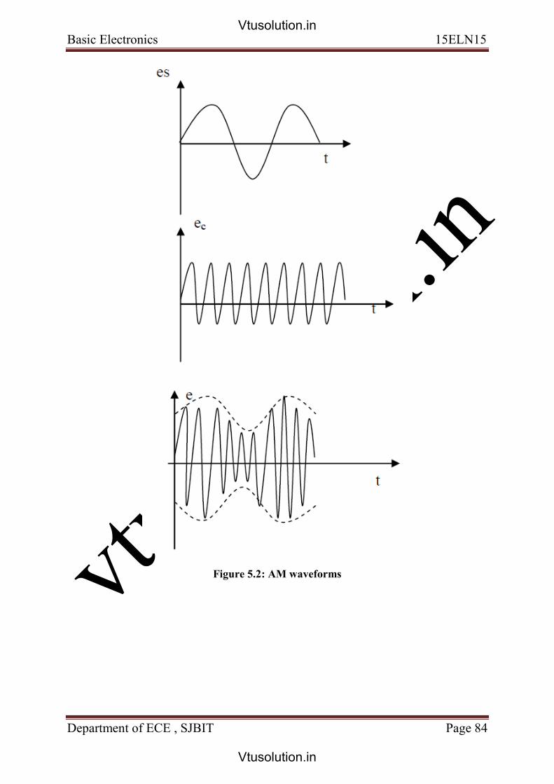
vtusol
ution
.in
Basic Electronics 15ELN15
Department of ECE , SJBIT Page 84
Figure 5.2: AM waveforms
Vtusolution.in
Vtusolution.in

vtusol
ution
.in
Basic Electronics 15ELN15
Department of ECE , SJBIT Page 85
Analysis of amplitude modulated wavesignal
mEc
EC Ec
Carrier AM Wave
Figure 5.3: AM waveforms
A carrier wave is represented by ec = Eccoswct-------------------(1)
Where ec ------instantaneous voltage of carrier.
Ec -----amplitude of carrier.
In amplitude modulation, the amplitude EC of the carrier wave is varied in accordance
with intensity of the signal as shown in figure.
Suppose m=modulation index, then change in carrier amplitude =mEc.
Amplitude or Emax of the signal = mEc.
es =mEccoswst---------------------------------(2)
where mEc is the amplitude of the signal.
es ---------instantaneous voltage of the signal.
Vtusolution.in
Vtusolution.in

vtusol
ution
.in
Basic Electronics 15ELN15
Department of ECE , SJBIT Page 86
The amplitude of the carrier varies at signal frequency fs. Therefore the amplitude of AM
wave is given by,
Ec +mEccoswst = Ec(1+mcoswst)
The instantaneous voltage of AM wave is,
e = Amplitude x coswct
The AM wave is equivalent ot thesummatoin of theree sinusoidal waves: aone having
amplitude EC and frequency fc, the second having amplitde mEc/2 and frequency (fc +
fs) and the third having amplitude mEc/2 and frequency fc – fs..
The AM wave consists three frequencies viz, fc, fc+fs . The first frequency is the
carrier frequency. Thus the process of modulation doesnot change the original carrier
frequency but produces two new frequencies fc+fs and fc – fs. which are called
sideband frequencies.
In amplitude modulation the bandwidth is from fc – fs. to fc+fs ie 2fs ie twice the
signal frequency.
)3()cos(2
)cos(2
cos
])cos()[cos(2
cos
]coscos2[2
cos
coscoscoscos)cos1(
twwmE
twwmE
twEe
twwtwwmE
twE
twtwmE
twE
twtwmEtwE
twtwmEe
scc
scc
cC
scscc
cC
csC
cC
csCcC
csC
Vtusolution.in
Vtusolution.in

vtusol
ution
.in
Basic Electronics 15ELN15
Department of ECE , SJBIT Page 87
)7(2)6(
)5(,
)6(2
22
21
242
)5(4
2222
)4(2
2
),3(
2
2
22
22222
22
22
2
2
m
m
equn
equn
P
P
sidebandsbycarriedpowertotaloffractionAlso
m
R
E
m
R
E
R
Em
R
E
PPPwaveAMofpowerTotal
R
Em
R
mE
R
mE
PsidebandsofpowerTotal
R
E
R
E
Ppowercarrier
equationfrom
T
S
C
CCC
SCT
C
CC
S
C
c
C
Frequency modulation
“When the frequency of carrier wave is changed in accordance with the intensity of the
signal, it is called frequency modulation‖.
Here the amplitude of the modulated wave remains the same ie carrier wave
amplitude.
The frequency variations of carrier wave depend upon the instantaneous amplitude of
the signal.
When the signal approaches positive peaks as the B and F, the carrier frequency is
increased to maximum and during negative peak, the carrier frequency is reduced to
minimum as shown by widely spaced cycles.
Vtusolution.in
Vtusolution.in

vtusol
ution
.in
Basic Electronics 15ELN15
Department of ECE , SJBIT Page 88
Figure 5.4: FM waveforms
Comparision of AM and FM.
Amplitude Modulation Frequency Modulation
1 The amplitude of the carrier is varied
In accordance with the signal
The frequency of the carrier is
varied in accordance with the signal
2 The modulation index ‗m„ is <1 The modulation index ‗β„ is >1
3 Transmitted power is dependent on
modulation index ‗m„
Transmitted power is independent
on modulation index ‗β„
4 Contains only two side bands Contains multiple side bands
5 Susceptible to noise due to The
method of modulation used.
Immune to noise as amplitudes are
Clipped
6 Less efficient as carrier contains more
power than side
More efficient as it contains more
side bands bands and hence more
signal power.
7 De-modulation is simple De-modulation is more complex.
Vtusolution.in
Vtusolution.in

vtusol
ution
.in
Basic Electronics 15ELN15
Department of ECE , SJBIT Page 89
AM diode detector
Fig. below shows a simple diode detector employing a diode and a filter circuit. A detector
circuit performs the following two functions.
1. It rectifies the modulated wave.
2. It separates the audio signal from the carrier.
The modulated wave of desired frequency is selected by the parallel tuned circuit L1C1 and
is applied to the diode. During positive half cycles of the modulated wave the diode conducts,
while during negative half cycles it does not. The result is the output of diode consists of
positive half cycle of modulated wave as shown in figure.
The rectified output consists of r.f. component and the audio signal which cannot be
fed to the speaker for sound reproduction. The r.f. component is filtered by the
capacitor ‗C„ shunted across the speaker. The value of ‗C„ is large enough to present
low reactance to the r.f. component . fc+fs Therefore signal is passed to the speaker
Fig 5.5: AM Diode detector
Vtusolution.in
Vtusolution.in

vtusol
ution
.in
Basic Electronics 15ELN15
Department of ECE , SJBIT Page 90
TRANSDUCERS INTRODUCTION
A transducer is a device that converts one form of energy to other form. It converts
the measured to a usable electrical signal. In other word it is a device that is capable
of converting the physical quantity into a proportional electrical quantity such as
voltage or current. Transducer contains two parts that are closely related to each other
i.e. the sensing element and transduction element. The sensing element is called as the
sensor. It is device producing measurable response to change in physical conditions.
The transduction element converts the sensor output to suitable electrical form.
Fig: 5.6: Transducers
Passive Electrical Transducers:
These transducers need external source of power for their operation. So they
are not self generating type transducers.
A DC power supply or an audio frequency generator is used as an external
power source.These transducers produce the output signal in the form of
variation in resistance, capacitance, inductance or some other electrical
parameter in response to the quantity to be measured.
1. Resistive Transducers
The variable resistance transducers are one of the most commonly used types of
transducers. The variable resistance transducers are also called as resistive transducers
or resistive sensors. They can be used for measuring various physical quantities like
temperature, pressure, displacement, force, vibrations etc. These transducers are
usually used as the secondary transducers, where the output from the primary
mechanical transducer acts as the input for the variable resistance transducer. The
output obtained from it is calibrated against the input quantity and it directly gives the
value of the input.
Vtusolution.in
Vtusolution.in

vtusol
ution
.in
Basic Electronics 15ELN15
Department of ECE , SJBIT Page 91
The variable resistance transducer elements work on the principle that the resistance of the
conductor is directly proportional to the length of the conductor and inversely proportional to
the area of the conductor. Thus if L is the length of the conductor (in m) and A is its area (in
m square), its resistance (in ohms) is given by:
R=ρl/a
Where
l -conductor length in m
a – area of crosssection in m2
ρ – specific resistivity in Ω-m
Resistance Thermometers :
Resistance thermometers, also called resistance temperature detectors (RTDs), are sensors
used to measure temperature by correlating the resistance of the RTD element with
temperature. Most RTD elements consist of a length of fine coiled wire wrapped around a
ceramic or glass core. The element is usually quite fragile, so it is often placed inside a
sheathed probe to protect it. The RTD element is made from a pure material, typically
platinum, nickel or copper. The material has a predictable change in resistance as the
temperature changes and it is this predictable change that is used to determine temperature.
They are slowly replacing the use of thermocouples in many industrial applications below
600 °C, due to higher accuracy and repeatability.
Fig 5.7 : Resistance Thermometers
Vtusolution.in
Vtusolution.in

vtusol
ution
.in
Basic Electronics 15ELN15
Department of ECE , SJBIT Page 92
Thermistor
A thermistor is a type of resistor whose resistance varies significantly with temperature,
more so than in standard resistors. The word is a portmanteau of thermal and resistor.
Thermistors are widely used as inrush current limiters, temperature sensors, self-resetting
overcurrent protectors, and self-regulating heating elements.
Where ,
R0 – resistance at T0(k)
R - resistance at T(k)
Β – constant to be determined experimentally.
For large values of T, we can approximate as
R = R0exp (β/T)
Linear Variable Differential Transformer
An LVDT, or Linear Variable Differential Transformer, is a transducer that converts a linear
displacement or position from a mechanical reference (or zero) into a proportional electrical
signal containing hase (for direction) and amplitude information (for distance). The LVDT
operation does not require electrical contact between the moving part (probe or core rod
assembly) and the transformer, but rather relies on electromagnetic coupling; this and the fact
that they operate without any built-in electronic circuitry are the primary reasons why LVDTs
have been widely used in applications where long life and high reliability under severe
environments are a required, such Military/Aerospace applications.
Fig5.8 : Linear Variable Differential Transformer
Vtusolution.in
Vtusolution.in

vtusol
ution
.in
Basic Electronics 15ELN15
Department of ECE , SJBIT Page 93
The LVDT consists of a primary coil (of magnet wire) wound over the whole length of a non-
ferromagnetic bore liner (or spool tube) or a cylindrical coil form. Two secondary coils are
wound on top of the primary coil for “long stroke” LVDTs (i.e. for actuator main RAM) or
each side of the primary coil for “Short stroke” LVDTs (i.e. for electro-hydraulic servo-valve
or EHSV). The two secondary windings are typically connected in “opposite series” (or
wound in opposite rotational directions). A ferromagnetic core, which length is a fraction of
the bore liner length, magnetically couples the primary to the secondary winding turns that
are located above the length of the core.
Active electrical transducer
1. Piezoelectric transducer
Certain single crystal materials exhibit the following phenomenon: when the crystal is
mechanically strained, or when the crystal is deformed by the applica tion of an external
stress, electric charges appear on certain of the crystal surfaces; and when the direction of the
strain reverses, the polarity of the electric charge is reversed. This is called the direct
piezoelectric effect , and the crystals that exhibit it are classed as piezoelectric crystals.
2. Photoelectric transducer
Provided is a photoelectric conversion element which suppresses the generation of a reverse
current and which has enhanced photoelectric conversion efficiency. The photoelectric
conversion element according to the present invention includes at least one support
conductive layer, photoelectric conversion layer, porous insulating layer, catalyst layer
counter conductive layer, and counter support in series. The photoelectric conversion layer
includes a porous semiconductor sub layer containing a semiconductor material and a
photosensitizing element adsorbed on the porous semiconductor sub layer. A carrier transport
material is placed between the porous insulating layer and the catalyst layer .The porous
semiconductor sub layer and the porous insulating layer contain pores. The pores are filled
with the carrier transport material .There is no strong bonding force, obtained by deposition
by a screen printing process, a vapour deposition process, or a sputtering process, between
the porous insulating layer and the catalyst layer .
Vtusolution.in
Vtusolution.in

vtusol
ution
.in
Basic Electronics 15ELN15
Department of ECE , SJBIT Page 94
Recommended Questions
1. What is modulation why it‟s required?
2. Write short note Amplitude modulation
3. What are diff b/w FM & AM?
4. Explain with neat diagram the principle of Frequency Modulation; write the
expressions for an FM wave.
5. Explain with neat diagram the principle of Amplitude Modulation; write the
expressions for an AM wave.
6. What are transducers?
7. Explain Passive Electrical Transducers?
8. Explain Active electrical transducer?
9. Explain piezoelectric transducer with a diagram.
10. Explain photoelectric transducer with a diagram.
11. Write a note on Linear Variable Differential Transformer
12. Write a note on Resistive Transducers?
13. Write a note on Resistance Thermometers?
Vtusolution.in
Vtusolution.in