submicrosecond rearrangeable nonblocking silicon-on-insulator thermo-optic 4×4 switch matrix
TRANSCRIPT

March 15, 2007 / Vol. 32, No. 6 / OPTICS LETTERS 603
Submicrosecond rearrangeable nonblockingsilicon-on-insulator thermo-optic 4Ã4
switch matrix
Yuntao Li, Jinzhong Yu, Shaowu Chen, Yanping Li, and Yuanyuan ChenState Key Laboratory of Optoelectronics, Institute of Semiconductors, Chinese Academy of Sciences,
Beijing 100083, China
Received September 14, 2006; revised November 28, 2006; accepted December 8, 2006;posted December 11, 2006 (Doc. ID 75074); published February 23, 2007
A rearrangeable nonblocking silicon-on-insulator-based thermo-optic 4�4 switch matrix is designed andfabricated. A spot-size converter is integrated to reduce the insertion loss, and a new driving circuit is de-signed to improve the response speed. The insertion loss is less than 10 dB, and the response time is 950 ns.© 2007 Optical Society of America
OCIS codes: 130.3120, 060.1810, 230.0320, 230.3120.
An optical switch matrix is one of the key devices foroptical communication systems, especially for opticalcross connection and optical add–drop multiplexingsystems. Many optical switch matrices have been re-ported and used in communication systems, includ-ing ones based on silica, polymer, and silicon-on-insulators (SOIs). Among these, thermo-optic switchmatrices based on SOIs are attracting more and moreattention due to their high speed and matureproduction.1–4 However, due to the natural character-istics of silicon, the response time of an SOI thermo-optic switch is hardly less than 1 �s. By improvingthe control method, a submicrosecond SOI 2�2switch was achieved and reported in Ref. 5. However,the fastest response time that has been reported for a4�4 switch matrix is 4.6 �s.6
In this Letter, we report the design and fabricationof a rearrangeable nonblocking SOI thermo-optic 4�4 switch matrix. A spot-size converter (SSC) is in-tegrated to reduce the insertion loss, and a new driv-ing circuit is designed to improve the response speedto submicrosecond. This is the first time, to the bestof our knowledge, that a submicrosecond SOI 4�4switch matrix is reported.
The switch matrix is fabricated on a back-etchingSOI (BE-SOI) wafer with an 8 �m thick top siliconlayer and a 0.5 �m thick buried silica layer. Figure 1shows the schematic of a 4�4 nonblocking switchmatrix, where the 2�2 switch cell is based on Mach–Zehnder interferometer structure. Grooves are intro-duced between the switch cells to alleviate heat dif-fusion between them to decrease the powerconsumption and cross talk. SSCs are integratedwith the switches in input and output ports to reducethe coupling loss.6
In this design, the width of the single-mode wave-guide is 3.5 �m, while the height and the etchingdepth of the rib waveguide are 4 and 2 �m, respec-tively. The length of the multimode interference is1920 �m and the width is 20 �m. A 70 nm thick oxidelayer is formed on the core layer to protect thewaveguides from optical absorption by heaters. The
size of the device is 30 mm�0.25 mm.0146-9592/07/060603-2/$15.00 ©
In Ref. 5, a differential control method and a con-troller were presented, which suppressed the risingand falling time from 29.2 and 35.0 �s to 725 and700 ns, respectively. But another problem occurs. Thestatic power consumption brought by the bias voltagewould be more than 100 mW,7,8 which is acceptablefor a 2�2 optical switch. However, for a 4�4 opticalswitch matrix, it would be more than 600 mW. Fur-thermore, for a larger-scale optical switch matrix, itwould be a disaster. To avoid large static power con-sumption and reduce the response time effectively, acustomized driving circuit for the switch cell is de-signed to decrease the response time. Figure 2 showsthe structure of the driving circuit. A field program-mable gate array (FPGA) is introduced to confirm thestates of switch matrices and generate driving sig-nals for driving circuits. At the rising edge of the con-trol signal, an extra pulse is applied to the heater fora period of time to overheat it. The larger tempera-ture difference between heater and waveguide makesthe temperature of the waveguide rise more quickly,so that the rising time is reduced. At the falling edgeof the signal, another extra bias is applied to theother heater. The first heater’s temperature is fallingwhile the other’s is rising, causing the phase of thelight passing through the two waveguides to changeinversely at the same time. As soon as the phase dif-ference is zero, the switch is changed to the crossstate, and the falling time is thus decreased.5 Com-
Fig. 1. Structure of 4�4 SOI nonblocking thermo-opticswitch matrix. The dashed and dotted lines shows the lightroute of signals at input port 1 in the initial state and whenswitch cell 4 is modulated, respectively. Signals at any in-put ports can come out from any output ports by modulat-
ing different switch cells.2007 Optical Society of America
604 OPTICS LETTERS / Vol. 32, No. 6 / March 15, 2007
pared with the method reported in Ref. 5, the staticpower consumption of the device is zero, and it issuitable for a large-scale optical switch matrix. Onthe other hand, an FPGA chip is enough to deal withall of the control signals of six switch cells. Further-more, the area and number of chips are much smallerthan those of Ref. 5, and a standard input–output in-terface makes it convenient for monointegration in
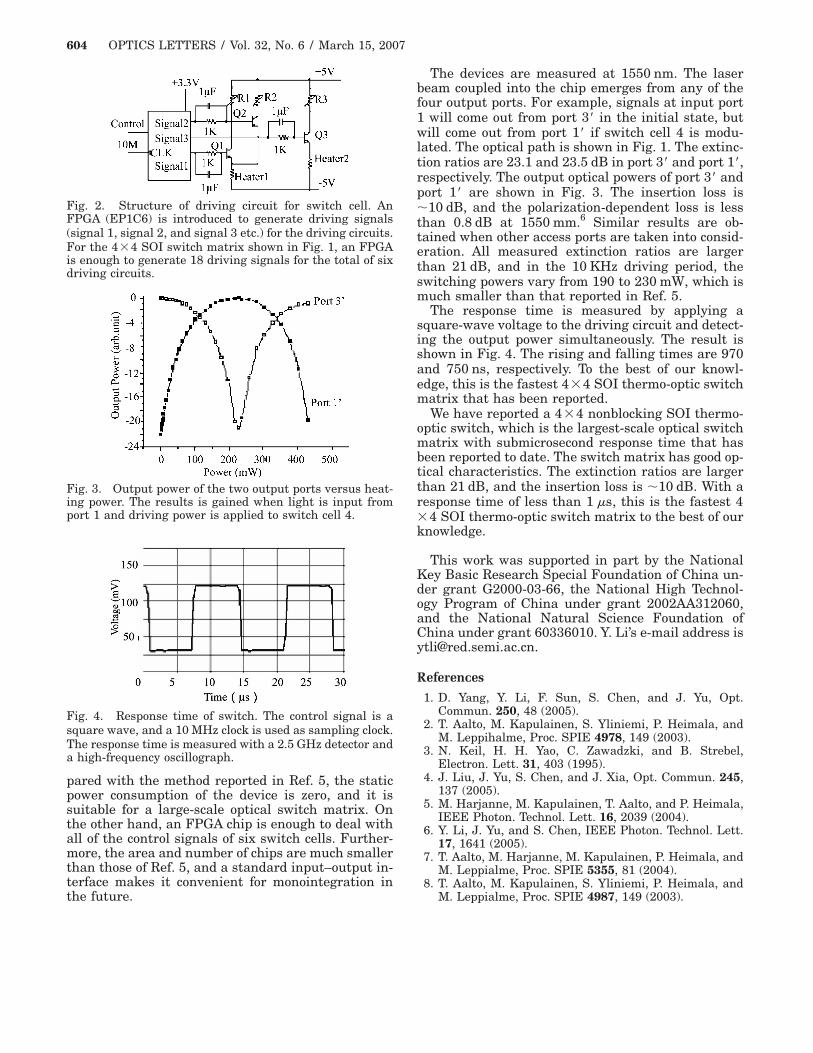
Fig. 2. Structure of driving circuit for switch cell. AnFPGA (EP1C6) is introduced to generate driving signals(signal 1, signal 2, and signal 3 etc.) for the driving circuits.For the 4�4 SOI switch matrix shown in Fig. 1, an FPGAis enough to generate 18 driving signals for the total of sixdriving circuits.
Fig. 3. Output power of the two output ports versus heat-ing power. The results is gained when light is input fromport 1 and driving power is applied to switch cell 4.
Fig. 4. Response time of switch. The control signal is asquare wave, and a 10 MHz clock is used as sampling clock.The response time is measured with a 2.5 GHz detector anda high-frequency oscillograph.
the future.
The devices are measured at 1550 nm. The laserbeam coupled into the chip emerges from any of thefour output ports. For example, signals at input port1 will come out from port 3� in the initial state, butwill come out from port 1� if switch cell 4 is modu-lated. The optical path is shown in Fig. 1. The extinc-tion ratios are 23.1 and 23.5 dB in port 3� and port 1�,respectively. The output optical powers of port 3� andport 1� are shown in Fig. 3. The insertion loss is�10 dB, and the polarization-dependent loss is lessthan 0.8 dB at 1550 mm.6 Similar results are ob-tained when other access ports are taken into consid-eration. All measured extinction ratios are largerthan 21 dB, and in the 10 KHz driving period, theswitching powers vary from 190 to 230 mW, which ismuch smaller than that reported in Ref. 5.
The response time is measured by applying asquare-wave voltage to the driving circuit and detect-ing the output power simultaneously. The result isshown in Fig. 4. The rising and falling times are 970and 750 ns, respectively. To the best of our knowl-edge, this is the fastest 4�4 SOI thermo-optic switchmatrix that has been reported.
We have reported a 4�4 nonblocking SOI thermo-optic switch, which is the largest-scale optical switchmatrix with submicrosecond response time that hasbeen reported to date. The switch matrix has good op-tical characteristics. The extinction ratios are largerthan 21 dB, and the insertion loss is �10 dB. With aresponse time of less than 1 �s, this is the fastest 4�4 SOI thermo-optic switch matrix to the best of ourknowledge.
This work was supported in part by the NationalKey Basic Research Special Foundation of China un-der grant G2000-03-66, the National High Technol-ogy Program of China under grant 2002AA312060,and the National Natural Science Foundation ofChina under grant 60336010. Y. Li’s e-mail address [email protected].
References
1. D. Yang, Y. Li, F. Sun, S. Chen, and J. Yu, Opt.Commun. 250, 48 (2005).
2. T. Aalto, M. Kapulainen, S. Yliniemi, P. Heimala, andM. Leppihalme, Proc. SPIE 4978, 149 (2003).
3. N. Keil, H. H. Yao, C. Zawadzki, and B. Strebel,Electron. Lett. 31, 403 (1995).
4. J. Liu, J. Yu, S. Chen, and J. Xia, Opt. Commun. 245,137 (2005).
5. M. Harjanne, M. Kapulainen, T. Aalto, and P. Heimala,IEEE Photon. Technol. Lett. 16, 2039 (2004).
6. Y. Li, J. Yu, and S. Chen, IEEE Photon. Technol. Lett.17, 1641 (2005).
7. T. Aalto, M. Harjanne, M. Kapulainen, P. Heimala, andM. Leppialme, Proc. SPIE 5355, 81 (2004).
8. T. Aalto, M. Kapulainen, S. Yliniemi, P. Heimala, and
M. Leppialme, Proc. SPIE 4987, 149 (2003).