submillimeter wave camera using a novel photon detector
TRANSCRIPT

Submillimeter wave camera using a novel photon
detector technology
A ThesisPresented to
The Academic Faculty
by
Shwetank Kumar
In Partial Fulfillmentof the Requirements for the Degree
Doctor of Philosophy
School of Applied PhysicsCalifornia Institute of Technology
Pasadena, California2007
(Defended December 13, 2007)

c© 2007Shwetank Kumar
All Rights Reserved
ii

Translation of The Psalm of Life by W.H. Longfellow to Hindi by my grandfather Sri. Ram Chand Bhatia.
(Printed with permission)
a
a
iii

iv

ACKNOWLEDGEMENTS
I am truly privileged to have worked with Prof. Jonas Zmuidzinas for my PhD.
Jonas’ clarity of thought as he approaches science is simultaneously inspirational and
humbling. His commitment as a mentor is unparalleled and I will never forget the
day he walked into my candidacy exam with an IV stuck to his arm to ensure that
he was there for me. I have learnt much from him – science and how to do it well –
and hope to continue to do so in future.
This thesis would not be possible without the other members of my research group.
I would like to thank Dr. Peter Day who was a great support for me as a co-advisor
when Jonas was away. I appreciate Dr. Rick Leduc’s inputs on mask designing and
fabrication of the devices. Dr. Ben Mazin’s work helped in gathering noise data
on niobium resonators. Useful discussions with Dr. Megan Eckart helped me in
clarifying many detector concepts. Many of the photon detector experiments were
carried out with Tasos Vayonakis, who is by far the most meticulous experimentalist
I have encountered and I have learnt much from him.
I would like to thank Dr. Simon Radford and my thesis committee, comprising of
Dr. David Rutledge, Dr. Marc Bockrath, and Dr. Axel Scherer, for useful suggestions
on my thesis.
One of the most memorable parts of my PhD was spent at the IBM Research
Center in the summer of 2007 where I found new friends and mentors – Dr. Stuart
Parkin, Dr. Mike Gaidis, Dr. Masamitsu Hayashi, and Dr. Rai Moriya. I appreciate
Mike nudging me to take up a summer internship in Stuart’s group, and candid
discussions with him gave me important insights into the nature of industrial research.
Stuart has the most contagious enthusiasm for science, and working with him was
v

really a turning point in my choice of what I wanted to do after my PhD. Masa and
Rai taught me a great deal about magnetics. Their understanding of the subject and
its issues is unparalleled and I appreciate learning from these gifted experimentalists.
I want to thank my high school friends – especially Nidhi, Neha, and Manish – who
have stuck with me through the highs and lows in my career and even on occasion, pre-
tended to feign interest in my research. All my friends at Caltech – especially Meher,
Jeff, Chip, Vikram, Nachiket, Uday, Mayank, Prabha, Saha, Sukhada, Pinkesh, and
Mansi – made my time here very memorable. Many useful suggestions to the thesis
were made by Mansi, Varun and Matt Ferry. I want to thank Dr. Carlo Callegari
from whom I learnt a lot, both academically and non-academically, in the early part
of my PhD work.
Through the entire time my extended family has been an unwavering source of
support and love. I am indebted to the members of Multanimafia for their constant
words of encouragement: My cousin sister Kriti was often on the other end of the
phone on my bad days. Rohit, my co-beacon of uncertainty has always been no more
than a phone call away as well day or night and has tolerated, learnt from, and taught
me esoteric jokes. I would not have made it very far without him. Toshi, my dearest
sibling whose importance in my life is immeasurable – at some level the only one who
truly gets me. My parents have been an endless source of love and encouragement
for me. I have learnt much from dad about science, religion, philosophy, and arts in
our endless late-night conversations. I hope one day I can match a fraction of his
knowledge and wisdom. Mum has showered me with unselfish love and made many
a sacrifice so that I had the freedom to do what I so wanted to. Their love has truly
been the scaffolding on which my dreams and this thesis have taken shape.
vi

ABSTRACT
Cryogenic photon detectors can be used to make extremely sensitive cameras
for submillimeter astronomy. Current detector technologies already have sensitivities
limited by the noise due to photon arrival statistics. To further improve the sensitiv-
ity and mapping speed of experiments for a wide field survey, focal planes containing
tens of thousands of pixels are required. Unfortunately, the current technologies use
discrete and massive components which are not easy to integrate into large arrays.
This thesis presents a 16-pixel, two-color, submillimeter-wave, prototype camera de-
veloped at Caltech and the Jet Propulsion Laboratory using a novel photon detector
technology. The camera also uses new designs for other constituent elements – the
antenna, transmission line feednetwork, and bandpass filters – to implement the sub-
millimeter pixels. These designs allow integration of the entire camera onto a single
chip and conclusively address the problem of scalability while maintaining the sen-
sitivity and noise performance of the current technologies. This thesis explains the
design of each of these components and presents the results from experiments con-
ducted to test their performance. Results from the ’first light’, obtained by mounting
the prototype camera onto the Caltech Submillimeter Observatory (CSO), are also
presented.
We have also studied the temperature and power dependence of the resonance fre-
quency, quality factor, and frequency noise of the superconducting niobium thin-film
coplanar waveguide (CPW) resonators in order to understand the factors affecting the
noise performance of our photon detectors. These experiments were carried out at
temperatures well below the superconducting transition (Tc = 9.2 K) in an attempt
to understand the source of the excess frequency noise of superconducting resonators
vii

which form the sensing element of our photon detectors. The noise decreases by nearly
two orders of magnitude as the temperature is increased from 120 to 1200 mK, while
the variation of the resonance frequency with temperature over this range agrees well
with the standard two-level systems (TLS) model for amorphous dielectrics. These
results support the hypothesis that TLS are responsible for the noise in supercon-
ducting microresonators and have important implications for resonator applications
such as qubits and photon detectors.
viii

TABLE OF CONTENTS
ACKNOWLEDGEMENTS . . . . . . . . . . . . . . . . . . . . . . . . . . v
ABSTRACT . . . . . . . . . . . . . . . . . . . . . . . . . . . . . . . . . . . vii
LIST OF TABLES . . . . . . . . . . . . . . . . . . . . . . . . . . . . . . . xii
LIST OF FIGURES . . . . . . . . . . . . . . . . . . . . . . . . . . . . . . xiii
I INTRODUCTION . . . . . . . . . . . . . . . . . . . . . . . . . . . . . 1
1.1 Motivation – Submillimeter Astronomy . . . . . . . . . . . . . . . . 1
1.2 Scientific Case for Novel Submillimeter Instrumentation . . . . . . . 4
1.2.1 Submillimeter Galaxies . . . . . . . . . . . . . . . . . . . . . 4
1.2.2 Milky Way Galactic Plane Survey . . . . . . . . . . . . . . . 6
1.2.3 Sunyaev-Zel’dovich Effect (SZE) Measurements . . . . . . . . 8
1.3 Instrumentation . . . . . . . . . . . . . . . . . . . . . . . . . . . . . 10
1.4 Thesis Outline . . . . . . . . . . . . . . . . . . . . . . . . . . . . . . 14
II PHYSICS OF SUPERCONDUCTING MICRORESONATORS . 15
2.1 Introduction . . . . . . . . . . . . . . . . . . . . . . . . . . . . . . . 15
2.2 Experimental Introduction . . . . . . . . . . . . . . . . . . . . . . . 18
2.3 Device Details . . . . . . . . . . . . . . . . . . . . . . . . . . . . . . 19
2.4 Experimental Setup . . . . . . . . . . . . . . . . . . . . . . . . . . . 20
2.5 Experiment . . . . . . . . . . . . . . . . . . . . . . . . . . . . . . . . 21
2.6 Results . . . . . . . . . . . . . . . . . . . . . . . . . . . . . . . . . . 23
2.6.1 Frequency vs Temperature . . . . . . . . . . . . . . . . . . . 23
2.6.2 Frequency vs Power . . . . . . . . . . . . . . . . . . . . . . . 26
2.6.3 Effects of TLS on Resonator Frequency and Quality Factor . 26
2.6.4 Frequency Noise vs Temperature . . . . . . . . . . . . . . . . 30
2.7 Conclusion . . . . . . . . . . . . . . . . . . . . . . . . . . . . . . . . 30
III PIXEL DESIGN . . . . . . . . . . . . . . . . . . . . . . . . . . . . . . 32
3.1 Introduction . . . . . . . . . . . . . . . . . . . . . . . . . . . . . . . 32
ix

3.2 Multi-slot Antenna . . . . . . . . . . . . . . . . . . . . . . . . . . . 36
3.3 Microstrip and feed network Design . . . . . . . . . . . . . . . . . . 41
3.4 Beam Map Measurement . . . . . . . . . . . . . . . . . . . . . . . . 44
3.5 Photon Detector Design . . . . . . . . . . . . . . . . . . . . . . . . . 47
3.5.1 Physics of Microwave Kinetic Inductance Detectors . . . . . . 47
3.5.2 Resonator Design . . . . . . . . . . . . . . . . . . . . . . . . 52
3.6 Fabrication Steps . . . . . . . . . . . . . . . . . . . . . . . . . . . . 59
3.7 Conclusions . . . . . . . . . . . . . . . . . . . . . . . . . . . . . . . 60
IV BANDPASS FILTER DESIGN . . . . . . . . . . . . . . . . . . . . . 63
4.1 Introduction . . . . . . . . . . . . . . . . . . . . . . . . . . . . . . . 63
4.2 Bandpass Filter Design . . . . . . . . . . . . . . . . . . . . . . . . . 65
4.2.1 Lumped–Element Circuit Design . . . . . . . . . . . . . . . . 65
4.2.2 Circuit Layout and Fabrication . . . . . . . . . . . . . . . . . 67
4.2.3 Component Design . . . . . . . . . . . . . . . . . . . . . . . 69
4.2.4 Effect of Superconductivity on the Filter Response . . . . . . 73
4.3 Measurements and Results . . . . . . . . . . . . . . . . . . . . . . . 75
4.4 Multi-Color Pixel Design . . . . . . . . . . . . . . . . . . . . . . . . 80
4.4.1 Two–Color Design and Results . . . . . . . . . . . . . . . . . 81
4.4.2 Four–Color Design . . . . . . . . . . . . . . . . . . . . . . . . 82
4.5 Conclusions . . . . . . . . . . . . . . . . . . . . . . . . . . . . . . . 86
V A 16–PIXEL, TWO–COLOR, SUBMILLIMETER DEMONSTRA-TION CAMERA . . . . . . . . . . . . . . . . . . . . . . . . . . . . . . 88
5.1 Introduction . . . . . . . . . . . . . . . . . . . . . . . . . . . . . . . 88
5.2 Camera Design and Layout . . . . . . . . . . . . . . . . . . . . . . . 89
5.3 Setup . . . . . . . . . . . . . . . . . . . . . . . . . . . . . . . . . . . 93
5.3.1 Electronics . . . . . . . . . . . . . . . . . . . . . . . . . . . . 93
5.3.2 Optics . . . . . . . . . . . . . . . . . . . . . . . . . . . . . . 95
5.3.3 Cryogenics . . . . . . . . . . . . . . . . . . . . . . . . . . . . 96
5.4 Results . . . . . . . . . . . . . . . . . . . . . . . . . . . . . . . . . . 98
x

5.5 Conclusion . . . . . . . . . . . . . . . . . . . . . . . . . . . . . . . . 99
VI FUTURE SCOPE . . . . . . . . . . . . . . . . . . . . . . . . . . . . . 101
6.1 Resonator Noise . . . . . . . . . . . . . . . . . . . . . . . . . . . . . 101
6.1.1 Conclusions . . . . . . . . . . . . . . . . . . . . . . . . . . . 101
6.1.2 Future Work . . . . . . . . . . . . . . . . . . . . . . . . . . . 102
6.2 Camera Design . . . . . . . . . . . . . . . . . . . . . . . . . . . . . . 102
6.2.1 Conclusion . . . . . . . . . . . . . . . . . . . . . . . . . . . . 102
6.2.2 Future Directions . . . . . . . . . . . . . . . . . . . . . . . . 103
6.3 Outlook . . . . . . . . . . . . . . . . . . . . . . . . . . . . . . . . . . 107
REFERENCES . . . . . . . . . . . . . . . . . . . . . . . . . . . . . . . . . . 108
xi

LIST OF TABLES
Table 3.1 Dimensions for the antenna layout . . . . . . . . . . . . . . . . . . 39
Table 3.2 Feednetwork dimensions . . . . . . . . . . . . . . . . . . . . . . . . 43
Table 3.3 Energy gaps of some typical superconductors in meV and GHz . . . 48
Table 3.4 Table for effects limiting resonator Q . . . . . . . . . . . . . . . . . 53
Table 3.5 Table for coupling strength for different CPW geometries . . . . . . 55
Table 3.6 Design parameters for the submillimeter coupler . . . . . . . . . . . 58
Table 4.1 Bandpass filter circuit element values . . . . . . . . . . . . . . . . . 66
Table 4.2 Spiral inductor dimensions . . . . . . . . . . . . . . . . . . . . . . . 70
Table 4.3 Capacitor dimensions . . . . . . . . . . . . . . . . . . . . . . . . . 73
Table 4.4 Coordinates of circuit elements in Figure 4.7 . . . . . . . . . . . . . 78
Table 5.1 Detector design parameters . . . . . . . . . . . . . . . . . . . . . . 89
xii

LIST OF FIGURES
Figure 1.1 The electromagnetic spectrum . . . . . . . . . . . . . . . . . . . . 1
Figure 1.2 Concept view of ALMA . . . . . . . . . . . . . . . . . . . . . . . 2
Figure 1.3 Concept view of CCAT . . . . . . . . . . . . . . . . . . . . . . . . 3
Figure 1.4 Images of Antennae galaxies . . . . . . . . . . . . . . . . . . . . . 5
Figure 1.5 Cosmic Optical, Infra-red and Microwave Background . . . . . . . 6
Figure 1.6 Galaxy number density vs luminosity plots . . . . . . . . . . . . . 7
Figure 1.7 Image of the galactic plane . . . . . . . . . . . . . . . . . . . . . . 7
Figure 1.8 Sunyaev-Zel’dovich effect schematic . . . . . . . . . . . . . . . . . 8
Figure 1.9 Submillimeter instrument’s pixel count Moore’s law . . . . . . . . 10
Figure 1.10 Images of SCUBA instrument . . . . . . . . . . . . . . . . . . . . 11
Figure 1.11 Images of Bolocam instrument . . . . . . . . . . . . . . . . . . . . 12
Figure 2.1 Applications of superconducting microresonators . . . . . . . . . . 15
Figure 2.2 Field distribution of a coplanar waveguide . . . . . . . . . . . . . 16
Figure 2.3 Equivalent circuit and image of a CPW microresonator . . . . . . 19
Figure 2.4 Block diagram for the experimental setup . . . . . . . . . . . . . 20
Figure 2.5 Fits to the resonator response . . . . . . . . . . . . . . . . . . . . 21
Figure 2.6 Amplitude and phase noise directions and spectra . . . . . . . . . 23
Figure 2.7 Amplitude and phase noise spectra at 120 and 600 mK . . . . . . 24
Figure 2.8 Frequency shift vs temperature at -72 and -92 dBm readout power 25
Figure 2.9 Frequency shift vs internal power at different temperatures . . . . 27
Figure 2.10 Quality factor vs temperature for different readout powers . . . . 29
Figure 2.11 Fractional frequency noise at different temperatures and powers . 29
Figure 3.1 Submillimeter detector system . . . . . . . . . . . . . . . . . . . . 32
Figure 3.2 A comparision of ACBAR with DemoCam . . . . . . . . . . . . . 35
Figure 3.3 Multi-slot antenna schematic . . . . . . . . . . . . . . . . . . . . 36
Figure 3.4 Side view of the antenna . . . . . . . . . . . . . . . . . . . . . . . 37
Figure 3.5 Antenna beam pattern using a diffraction grating model . . . . . 38
xiii

Figure 3.6 Feed network schematic with 16 taps . . . . . . . . . . . . . . . . 41
Figure 3.7 Schematic of the feed network . . . . . . . . . . . . . . . . . . . . 42
Figure 3.8 Antenna slot and feednetwork image . . . . . . . . . . . . . . . . 42
Figure 3.9 Optical chain used to measure the beam maps . . . . . . . . . . . 45
Figure 3.10 Antenna beam maps . . . . . . . . . . . . . . . . . . . . . . . . . 46
Figure 3.11 Illustration of detection principle . . . . . . . . . . . . . . . . . . 48
Figure 3.12 Surface impedance and quasi-particle density vs temperature . . . 49
Figure 3.13 Plot of resonator response (S21) in complex plane . . . . . . . . . 51
Figure 3.14 Resonator response with change in submillimeter power . . . . . . 53
Figure 3.15 Hybrid MKIDs resonator . . . . . . . . . . . . . . . . . . . . . . . 54
Figure 3.16 Submillimeter coupling section of the resonator . . . . . . . . . . 54
Figure 3.17 Simulation layout for the resonator coupling section . . . . . . . . 57
Figure 3.18 Layers for pixel fabrication . . . . . . . . . . . . . . . . . . . . . . 59
Figure 3.19 Pixel Schematic . . . . . . . . . . . . . . . . . . . . . . . . . . . . 61
Figure 3.20 Pixel photograph . . . . . . . . . . . . . . . . . . . . . . . . . . . 62
Figure 4.1 Atmospheric transmission spectrum with relevant bandpasses overlaid 63
Figure 4.2 Lumped element bandpass filter design . . . . . . . . . . . . . . . 65
Figure 4.3 Bandpass filter SONNET layout . . . . . . . . . . . . . . . . . . . 68
Figure 4.4 Spiral inductor layout . . . . . . . . . . . . . . . . . . . . . . . . 69
Figure 4.5 Illustration for SONNET simulation of superconducting circuits . 74
Figure 4.6 Simulated responses of the bandpass filters . . . . . . . . . . . . . 76
Figure 4.7 Layout for the filters marking the locations of circuit elements . . 77
Figure 4.8 Bandpass filter photograph . . . . . . . . . . . . . . . . . . . . . 77
Figure 4.9 Normalised measured and predicted bandpass filter responses . . 79
Figure 4.10 Dewar optical chain . . . . . . . . . . . . . . . . . . . . . . . . . . 79
Figure 4.11 Pixel response without an inline bandpass filter . . . . . . . . . . 80
Figure 4.12 Two-color pixel schematic . . . . . . . . . . . . . . . . . . . . . . 81
Figure 4.13 Simulated bandpass filter input impedance . . . . . . . . . . . . . 82
Figure 4.14 Two-color pixel measured response . . . . . . . . . . . . . . . . . 83
xiv

Figure 4.15 Network of bandpass filters for a four-color pixel . . . . . . . . . . 84
Figure 4.16 Networked four-color pixel response . . . . . . . . . . . . . . . . . 85
Figure 4.17 Response of the four-color pixel without network . . . . . . . . . 85
Figure 5.1 Caltech submillimeter observatory . . . . . . . . . . . . . . . . . . 88
Figure 5.2 Camera schematic . . . . . . . . . . . . . . . . . . . . . . . . . . 90
Figure 5.3 Resonance frequencies of photon detectors with on chip locations 91
Figure 5.4 Picture of the DemoCam chip with sub-components . . . . . . . . 92
Figure 5.5 Picture of the wafer on which the camera was fabricated . . . . . 93
Figure 5.6 Room temperature readout electronics block diagram . . . . . . . 94
Figure 5.7 Dewar optical chain . . . . . . . . . . . . . . . . . . . . . . . . . . 95
Figure 5.8 Photographs of the cryostat . . . . . . . . . . . . . . . . . . . . . 96
Figure 5.9 Photograph of the device housing . . . . . . . . . . . . . . . . . . 97
Figure 5.10 Images of Jupiter and G34.4 . . . . . . . . . . . . . . . . . . . . . 99
xv

CHAPTER I
INTRODUCTION
1.1 Motivation – Submillimeter Astronomy
Gamma
Rays
< 10nm
X-Rays
0.01 – 10
nm
Ultra-Violet
10 nm – 0.4
µm
Visible
0.4 – 0.7
µm
Infra-Red
0.7 µm – 0.1
mm
Microwave
1 mm – 0.1 m
Radio-
wave
> 0.1 m
Submm wavelengths: 0.1 – 1 mm (100 GHz – 1 THz)
Figure 1.1: The electromagnetic spectrum
Astronomy has historically been dominated by observations in the optical part of
the electromagnetic spectrum. There are various reasons why the optical frequency
range has been the most extensively studied for centuries [1, 2, 3]. The instrumen-
tation for this band has existed for a long time: The earliest photon detectors were
naked eyes, and Galileo used the optical telescope for astronomy for the first time
in the 17th century. It is easy to do ground-based astronomy in this band since the
Earth’s atmosphere is transmissive at these frequencies. However, a strong case can
be built for submillimeter astronomy as well, since the Earth’s atmosphere is par-
tially transmissive at microwave/radio, submillimeter, and infrared (IR) wavelengths
[2]. Furthermore, the optical frequencies form a small part of the entire electromag-
netic spectrum (Figure 1.1). They extend from 0.4 µm to 0.7 µm which is less than
a decade, while the radio-frequency (RF)/microwave, and submillimeter part of the
frequency spectrum extends over many decades (with the submillimeter part of the
spectrum extending over a decade, from 100 GHz to 1 THz) [1]. In the past it has been
1

difficult to do astronomy at submillimeter wavelengths because of the opacity due to
water lines in the Earth’s atmosphere and lack of high-performance instruments. The
problem of opacity due to water lines can be solved by doing ground-based astron-
omy from high altitude (∼ 14,000 ft), dry regions such as Mauna Kea, where the
Caltech Submillimeter Observatory (CSO) is located. The instrumentation and tech-
niques that already exist for the microwave/RF and optical frequency range can not
be readily adapted to the submillimeter band.
Figure 1.2: Concept view of ALMA (Credit: http://www.eso.org/projects/alma/)
However past two decades have seen tremendous progress in the performance of
submillimeter detectors [4, 5] and these changes are ushering in major investments
such as the Atacama Large Millimeter Array (ALMA) (Figure 1.2) interferometer
and the Caltech Cornell Atacama Telescope (CCAT) (Figure 1.3). ALMA is a $1
billion project which will have very high angular and spectral resolution (30” at 1.3
mm) and will be able to make exquisite images of very small fields [6]. CCAT on the
other hand will be a 25 m diameter, high-sensitivity, wide-field-of-view and a broad-
band telescope [7], and will provide capability for deep, multi-color, wide field surveys
which will help choose targets for more detailed follow-ups with ALMA. With these
2
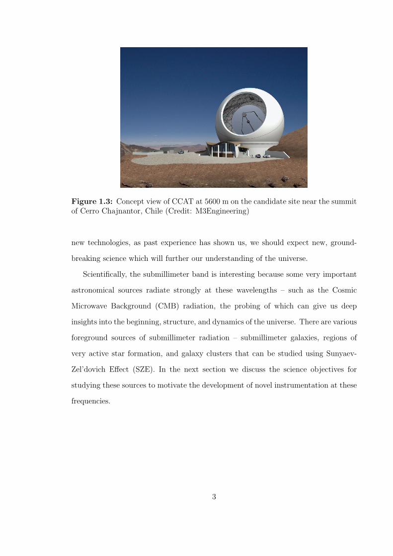
Figure 1.3: Concept view of CCAT at 5600 m on the candidate site near the summitof Cerro Chajnantor, Chile (Credit: M3Engineering)
new technologies, as past experience has shown us, we should expect new, ground-
breaking science which will further our understanding of the universe.
Scientifically, the submillimeter band is interesting because some very important
astronomical sources radiate strongly at these wavelengths – such as the Cosmic
Microwave Background (CMB) radiation, the probing of which can give us deep
insights into the beginning, structure, and dynamics of the universe. There are various
foreground sources of submillimeter radiation – submillimeter galaxies, regions of
very active star formation, and galaxy clusters that can be studied using Sunyaev-
Zel’dovich Effect (SZE). In the next section we discuss the science objectives for
studying these sources to motivate the development of novel instrumentation at these
frequencies.
3
1.2 Scientific Case for Novel Submillimeter In-
strumentation
1.2.1 Submillimeter Galaxies
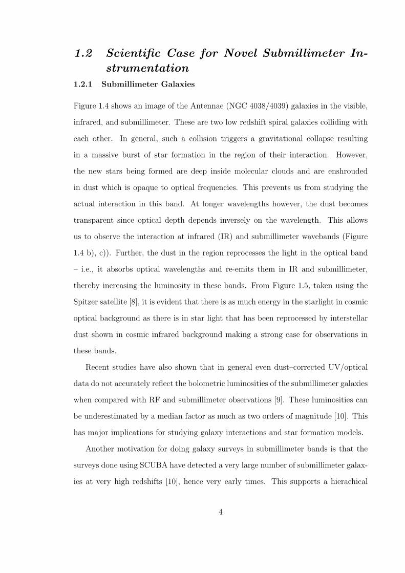
Figure 1.4 shows an image of the Antennae (NGC 4038/4039) galaxies in the visible,
infrared, and submillimeter. These are two low redshift spiral galaxies colliding with
each other. In general, such a collision triggers a gravitational collapse resulting
in a massive burst of star formation in the region of their interaction. However,
the new stars being formed are deep inside molecular clouds and are enshrouded
in dust which is opaque to optical frequencies. This prevents us from studying the
actual interaction in this band. At longer wavelengths however, the dust becomes
transparent since optical depth depends inversely on the wavelength. This allows
us to observe the interaction at infrared (IR) and submillimeter wavebands (Figure
1.4 b), c)). Further, the dust in the region reprocesses the light in the optical band
– i.e., it absorbs optical wavelengths and re-emits them in IR and submillimeter,
thereby increasing the luminosity in these bands. From Figure 1.5, taken using the
Spitzer satellite [8], it is evident that there is as much energy in the starlight in cosmic
optical background as there is in star light that has been reprocessed by interstellar
dust shown in cosmic infrared background making a strong case for observations in
these bands.
Recent studies have also shown that in general even dust–corrected UV/optical
data do not accurately reflect the bolometric luminosities of the submillimeter galaxies
when compared with RF and submillimeter observations [9]. These luminosities can
be underestimated by a median factor as much as two orders of magnitude [10]. This
has major implications for studying galaxy interactions and star formation models.
Another motivation for doing galaxy surveys in submillimeter bands is that the
surveys done using SCUBA have detected a very large number of submillimeter galax-
ies at very high redshifts [10], hence very early times. This supports a hierachical
4

Visible Infrared Sub-mm
a) b) c)
Figure 1.4: Images of the Antennae (NGC 4038/4039) in the visible (left), infrared(center), and submillimeter (right) (Credits: visible [HST,WFPC2], infrared [Spitzer,IRAC], and submillimeter [CSO, SHARC])
model for development of structure in the universe in which galaxy mergers such as
those mentioned above are very important and are a major source of star forma-
tion. The observed luminosity function, which gives number density of galaxies as a
function of luminosity (Figure 1.6), is far larger than what is predicted by the mod-
els tuned to explain the observations in the optical bands. These galaxy formation
models have needed dramatic changes, including changes in treatment of dark matter
halos and galaxy mergers [11], in order to explain the observations in the submil-
limeter band. To further test the new models incisively, it is required that we probe
the high-redshift tail of the galaxy population simultaneously in multiple frequency
bands in the submillimeter part of the spectrum.
A major astronomical challenge that may be addressed by simultaneous multi-
band measurements in the submillimeter is characterization of dust emissivity prop-
erties. The dust emissivity in this band is dominated by large grains in thermal
equilibrium which are characterised by a temperature and spectral dependence of
emissivity modeled simply by an index (β). This characterization is essential to esti-
mate redshifts using radio and submillimeter flux measurements. Since the accuracy
5

Figure 1.5: Power spectrum of Cosmic Optical, Infrared, and Microwave Back-ground from observations using the instrumentation on Spitzer satellite [8]. Thefrequency band between the dashed line shows the submillimeter range.
and precision of β are unknown, measuring it for a large sample of galaxies with low
redshifts and varying properties – so that the observations are on the Rayleigh-Jeans
(RJ) side of the thermal spectral emission density (SED) – will yield its intrinsic dis-
persion. This will allow us to assign systematic uncertainties to β, hence quantifying
systematic uncertainties in the dust temperature and redshift.
1.2.2 Milky Way Galactic Plane Survey
Galactic plane surveys have been undertaken by many teams – specifically using the
SCUBAII instrument on the James Clark Maxwell Telescope (JCMT), and Bolocam
on CSO. The science goals of these projects are to measure the galaxy-wide rates of
star formation, efficiency, triggers, evolution, and timescales of young massive stars
[7]. This would obtain the complete inventory of hot and cold dust in the galac-
tic plane. Combining this data with optical, radio, and IR data sets will determine
6

2000 m odel 2005 m odel
a) b)
Figure 1.6: Plots of number density vs luminosity with fits based on models con-structed (a) without and (b) with submillimeter survey data [11]
Figure 1.7: An image of the galactic plane using Bolocam in the 1.1 mm wavelengthband. The image dimensions are 2 × 1 with the field of view centered at a Galacticlongitude of l = 0.5, latitude b=0. It contains the Sgr A complex on the right, andSgr B2 star–forming complex in the left half of the image. (Credits: Dr. John Ballyand the Bolocam Galactic Plane Survey Team)
the relative importance of different mechanisms of star formation and their depen-
dence on properties of the inter-stellar medium [7]. Following up these measurements
7

across the submillimeter band from 350 µm to 1.4 mm will allow sampling of spec-
tral energy distributions to measure bolometric luminosities, dust temperatures, and
masses robustly. This would allow testing the hypothesis that the long wavelength
spectral emissivity index β can change significantly with temperature. Simultaneous
multi-color data would prove to be invaluable for this science.
1.2.3 Sunyaev-Zel’dovich Effect (SZE) Measurements
CMB photons
T = (1 + z) 2.725K
galaxy cluster
with hot ICM
z ~ 0 - 3
scattered
photons
(hotter)
last scattering
surface
z ~ 1100
observer
z = 0
a) b)
Figure 1.8: a) Original and the shifted spectrum of the CMB photons due to SZscattering off of the hot interstellar gas. b) Figure illustrating the SZ effect (Credit:Dr. Sunil Golwala)
The Cosmic Microwave Background (CMB) radiation was discovered in 1964 by
Wilson and Penzias and is regarded as the most conclusive piece of evidence for the
Big Bang Model. In 1989 the COBE satellite measured the CMB and showed that
it has a blackbody spectrum with temperature of 2.725 K to 1 part in 105 while
measuring its primary anisotropies. In 1970, Sunyaev and Zel’dovich predicted that
the CMB power spectrum would have secondary anisotropies due to what is now
known as Sunyaev-Zel’dovich Effect (SZE). This refers to the Thomson scattering of
Cosmic Microwave Background (CMB) photons by hot electrons in the intracluster
8

medium. This transfers some of the energy from the ionized gas to the CMB photons
while conserving the photon number (upscattering). While the effect itself is small
and of low probability (∼ 1%), it leads to a measurable change in the frequency
spectrum of the radiation and makes it non-thermal, so it effectively seems colder at
long wavelengths and hotter at short wavelengths. The temperature shift independent
of redshift is given by:
∆TSZE
TCMB
= f(x)y = f(x)
∫
nekTe
mec2σTdl (1.1)
where ne/me/Te/pe are electron density/mass/temperature/pressure, σT is the Thom-
son scattering cross section, k is the Boltzmann constant, c is the speed of light,
dl = cdt is the distance along the photon path through the cloud, and f(x) is the
spectral dependence with x = hν/kT . The photon energies get boosted by kTe
mec2,
which for temperatures 108 K can lead to relativistic increase in the energy. Since
the ratio ∆TSZE/TCMB, or equivalently the surface brightness of SZE, is redshift in-
dependent it is a powerful way to detect massive clusters at any redshift as long as
the experiment has sufficient angular resolution. There is also a second-order kinetic
SZE where the CMB photons interact with the electrons that have high energies due
to their bulk motion compared to the rest frame of CMB photons.
These effects can be used to constrain cosmological models and probe universal
constants in several different ways. Combined with X-ray cluster studies which probe
the emission measure of intracluster gas, SZE studies can be used to precisely deter-
mine the Hubble constant H0 and the deceleration parameter q0 [9, 12]. The SZE
combined with the X-ray estimates of gas temperature can be used to estimate the
baryonic mass fraction in the galaxy cluster [13]. Using SZE to detect distant clusters
allows us to study the large-scale structure and cosmological parameters describing
the universe – and might even be useful in constraining the dark matter equation of
state [12].
9

Kinetic SZE can be used to determine the cluster peculiar velocity [13]. These
measurements need to be made in the submillimeter band close to 150 GHz to measure
the SZ decrement or at 275 GHz to measure the SZ increment. Multi-color capabil-
ities in other bands will be useful for removing the atmospheric noise for increased
sensitivity and removing contaminants such as point sources. The next section lists
characteristics required in the instrumentation to meet these science goals.
1.3 Instrumentation
DemoCam
MKIDCam
Figure 1.9: The increase in pixel count of almost background limited bolometricsubmillimeter camera technologies over the past 20 years is seen to follow Moore’slaw. Also shown in the dotted red boxes are the DemoCam discussed in this thesisand future generation MKIDCam that will complement and compete with SCUBAIIusing kinetic inductance detector technology [14, 15, 16, 17].
Nearly background limited bolometric submillimeter camera technologies have fol-
lowed Moore’s law (Figure 1.9) and doubled in array size roughly every 20 months
or so. Current state of the art is defined by SCUBA at JCMT and Bolocam and
10

SHARCII at CSO (Figures 1.10, 1.11). These cameras have contributed significantly
to our scientific knowledge through galactic plane surveys [18, 19], surveys of submil-
limeter galaxies [20, 10, 21], and SZE observations [22]. However, these cameras have
a few hundred pixels and the technologies being used to implement them are difficult
to scale to larger array sizes. Future scientific missions motivated in Sections 1.2.1,
1.2.2 and 1.2.3 will require cameras with tens of thousands of background limited
multi-color pixels, if not more.
R e d s h ift d is trib u tio n
C h a p m an e t a l. 2 0 0 5
a)
b)
c)
d)
Figure 1.10: a) SCUBA instrument mounted on JCMT. b) SCUBA focal plane topview showing the input feedhorn antenna. c) Maps of submillimeter galaxies detectedusing SCUBA instrument. d)The redshift histogram of submillimeter galaxy sampleobserved using SCUBA [10]
Since it is difficult to scale current technologies to those sizes, new technologies
need to be developed making it feasible to construct large pixel arrays which allow
all the components of a submillimeter camera to be integrable onto a monolithic chip
so that scaling is not an issue.
11

a) b) c)
Figure 1.11: a) Bolocam detector b)Bolocam focal plane showing feeds (top) anddetectors (bottom) c) Bolocam camera mounted in the dewar with metal mesh filteron the top
This thesis presents a 16-pixel, 2-color camera (DemoCam) which we have de-
signed, implemented and tested. This camera uses novel, planar technologies for
pixel components – the antenna, feed network, bandpass filter, and photon detector
that allow for the entire camera to be fabricated on a single chip, thereby conclu-
sively addressing the problem of scalability photolithographically while maintaining
the sensitivity and noise performance of the other current technologies. Data can be
gathered in both the bands simultaneously for all the 16 pixels. The future gener-
ations (MKIDCam) will be able to operate simultaneously in all four submillimeter
bands (Chapter 4), which is essential for attaining future scientific goals. MKIDCam
will be a superior replacement for Bolocam as a facility instrument at the CSO and
will have comparable raw mapping speed to SCUBAII, mounted on JCMT, while
costing about an order of magnitude lesser. SCUBAII will operate with only two
colors, out of which only one will be regularly usable.
Future cameras for CCAT after MKIDCam will have tens of thousands of pixels
that will completely cover the telescope field of view (20’) which is necessary to make
use of its focal plane efficiently. The mapping speed of the instrument increases
12

linearly with the pixel count. Consequently, compared to the current rate of 1 or 2
submillimeter galaxy detections per night, with MKIDCam the mapping speed will
increase approximately by a factor of 6 resulting in detection of around 12 galaxies
per night[23] at the CSO. This number will be dramatically higher when the same
instrumentation is used on the upcoming CCAT.
Further, by using multi-color camera technologies it will be possible to ensure that
the detections made are robust, for example by requiring simultaneous detection in
multiple bands to rule out fake detections or omissions. Currently, monochromatic
observations are used which are then followed up in different bands by separate in-
struments. Different instruments typically have different sensitivities and systematics
and consequently lead to non-uniformity in data. This leads to discrepancies like spu-
rious detections and omissions in data sets, especially when working close to the noise
limit. Use of the multicolor cameras for a single survey will overcome this challenge
in multiple ways:
1. It avoids temporal variability – changes in the response due to changes in at-
mospheric conditions or instrument sensitivity – between the observations.
2. Although sensitivity of the intrument may be limited by other factors such as
the atmosphere, telescope quality etc. using a single camera in different bands
will lead to nominally uniform detector sensitivities which will make it possible
to make the survey depth more uniform at different wavelengths.
3. Systematics are easier to understand and remove between different bands from
the same survey.
4. There would be nominally uniform sky coverage while looking at the same
location in the sky which will make data in all bands for every covered spatial
location available except for the difference in beam sizes which would make the
diffraction spot size somewhat different.
13

Thus with simultaneous, uniformly calibrated photometry in multiple-frequency
bands, these issues will be addressed robustly, and interesting candidates (e.g., high-
redshift submillimeter galaxies) can be selected from the dataset for more expensive
follow-ups (e.g., making detailed maps using the ALMA interferometer).
1.4 Thesis Outline
This thesis presents a 16-pixel, two-color camera implemented using novel planar
technologies for the pixel subcomponents - the antenna, submillimeter feed networks
and waveguide and the photon detector, that integrate the entire camera on to a
single chip. The design is scalable to large arrays even as it maintains the perfor-
mance metrics of single pixels of current technologies. In Chapter 2 of this thesis
we discuss results of noise, resonance frequency and quality factor measurements of
superconducting resonators as a function of temperature and readout power of these
devices. These are of interest since superconducting microresonators form the sensing
element of the photon detectors used in our pixels and understanding the source and
mechanism of this noise will allow us to optimize our detectors for better perfomance.
Chapter 3 presents the design details of each sub-component (except the bandpass
filter) of a single pixel and discusses the measurement setup and results. Chapter
4 details the design of the on-chip bandpass filters and the details of designing a
multi-color pixel. The measurements performed on the two-color pixel and the design
for the four-color pixel, to be used in future generations of cameras are presented.
Chapter 5 presents integration of the 16 two-color pixels on to a single chip and the
detector design considerations. An overview of electronics and cryogenics which was
used to show the camera its first light on CSO is presented and results from the CSO
run showing maps of Jupiter and G34.3 are presented. The final chapter outlines
some interesting future directions possible for the work that was done for this thesis.
14

CHAPTER II
PHYSICS OF SUPERCONDUCTING
MICRORESONATORS
2.1 Introduction
Walraff et. al (Nature, 2004)
Mazin (Caltech Thesis 2004)
http://qt.tn.tudelft.nl/research/fluxqubit/fluxqubit.html
Day et. al (Nature, 2003)
Irwin ( Sci . Am., 2006)Irwin ( Sci . Am., 2006)
4x4 Submm KIDs
a) b) c)
d) e) f )
Figure 2.1: A variety of applications for superconducting microresonators are shown:a) Multiplexer for array of SQUIDs [24], b) Persistent current qubit using RF SQUIDs[25], c) Charge qubit coupled to superconducting microwave resonator [26], d) KineticInductance Strip Detector [27], e) Quarter wave superconducting resonator coupled toa CPW feedline [28], f) 16-pixel submillimeter test chip made using Kinetic InductanceDetectors as a presursor to DemoCam
The submillimeter detectors described in this thesis use superconducting microres-
onators as the sensing element. However, the superconducting microresonators are
versatile devices with diverse applications. They have been used for making SQUID
multiplexers [24], qubits [26, 29], photon detection [28, 30, 31], and for studying basic
15

physics [32, 33, 34]. As SQUID multiplexers they find applications in making mul-
tiplexed readouts for large pixel count arrays of low-temperature detectors needed
for novel particle and material physics, astronomy, and material science [24] (Figure
2.1a,b). In quantum computing superconducting microresonators have been used for
reading out charge qubits [26], resolving the number states of microwave photons [35],
stabilising flux qubits [36], and reading out RF qubits [29]. There are also propos-
als for making quantum memories [37] (Figure 2.1c) and coupling to polar molecules
[38] using them, and they have also been used to investigate a variety of basic physics
problems from non-linear oscillators [32] and their applications for making parametric
amplifiers and squeezed states [33] to the physics of the Casimir effect [34].
Si
Niobium (200 nm)
Silicon
Interface Amorphous Layer ?
Figure 2.2: a) Cross section of the CPW geometry. The center conductor is made ofsuperconducting metal (Nb) and is separated from the metallic ground plane throughair slots deposited on a substrate – typically silicon or sapphire. b) HFSS simulationof the electromagnetic field of CPW line shown in cross section. High field regions areseen close to the metal edges – TLSs in these regions with dipole moment pointingin direction of the field and energy splitting resonant with the field will couple to itmost strongly.
The early experiments in our group proceeded by noting that, instead of using
superconductors close to their transition temperature as bolometric detectors [39],
the kinetic inductance effect may be used to readout the change in the quasi-particle
density of a superconducting film produced as a consequence of absorption of pair-
breaking photons. This can be done by fabricating a thin film resonator using the
superconductor and measuring the change in its resonant response to a microwave
probe signal [40, 41, 42]. Indeed, the detector proof of principle was demonstrated
16

by energy-resolved detection of a 6 keV X-ray photon [28, 31, 43]. However, the
experiments showed an unexplained excess noise which limited the performance of
our detector [28, 27] and will in general limit the sensitivity of any experiment using
the superconducting resonator as sensing or readout element. This noise has been
measured and is seen to be primarily in the resonator frequency jitter or equivalently,
the phase direction [44]. While the exact source of origin and the mechanism of noise
generation is unknown, a likely possibility is that the noise is produced by two-level
systems (TLS) in the amorphous native oxide layers on the metal films or susbstrate
surfaces [45, 44] that couple to the electromagnetic field of the resonator through
dipole coupling (Figure 2.2).
Indeed, TLS models provide a quantitative explanation for the unusual ther-
mal, ultrasonic, and dielectric properties of amorphous materials at low-temperatures
[46, 47, 48, 49], and recent qubit experiments [45] have focused attention on the im-
portant role of TLS in superconducting microcircuits. The TLS level populations and
relaxation rates should vary strongly with the device temperature T , and the level
populations of near-resonant TLS should saturate [44] for sufficiently strong resonator
excitation power Pµw.
This chapter presents the measurements of the temperature and power dependence
of the resonance frequency, quality factor, and frequency noise of superconducting
niobium thin-film coplanar waveguide (CPW) resonators. In order to focus on the
role of the dielectric materials, the measurements were carried out at temperatures
well below the superconducting transition temperature (Tc = 9.2 K). We find that the
frequency noise of the resonators is strongly temperature dependent, decreasing by
nearly two orders of magnitude as the temperature is increased from 120 to 1200 mK,
approximately described by a power law T−1.76. We also find that the resonance
frequency has a significant variation over this temperature range which agrees well
with the standard two-level system (TLS) model for amorphous dielectrics. Hence,
17

measurements of the power and temperature variation of resonator frequency and
noise, as presented in this chapter, provide an important test of the TLS hypothesis
and do indeed suggest that the TLS are responsible for the noise in superconducting
microresonators. These results have important implications for optimizing device
design for use as qubits and photon detectors.
2.2 Experimental Introduction
We studied quarter-wavelength resonators made using coplanar waveguide (CPW)
geometry [28, 44]. These have a center metal conductor separated from the ground
plane by two air slots on either side, with most of the electromagnetic field residing
in the slots (Figure 2.2).
Figure 2.3 shows the equivalent circuit and a photograph of an actual device very
similar to the ones that were measured. The resonators are capacitively coupled to
a CPW feedline and are measured using a standard IQ (In-phase and Quadrature-
phase) homodyne mixing technique [28, 27] (Figure 2.4). With proper calibration, the
complex output voltage of the IQ mixer, Z = I + jQ, is proportional to the forward
scattering parameter S21. For excitation frequencies far removed from the resonance
frequency fr, the microwave signal passes unimpeded through the feedline, but close
to fr the resonator loads the feedline resulting in a transmission null. Equivalently,
in the complex plane when the microwave synthesizer’s frequency f is swept through
the resonance, Z(f) follows a circular trajectory [44]. As explained in more detail
below, the resonator’s frequency fr and quality factor Qr may be extracted by fitting
an analytical expression to the measured trajectory Z(f). The combined noise of
the resonator and readout electronics may be measured by setting the synthesizer
frequency f to the resonance frequency fr, then digitizing and analysing the fluctua-
tions δξ(t) = [δI(t), δQ(t)]T [28, 27, 44]. The noise of the readout electronics may be
measured separately by tuning the synthesizer frequency off resonance.
18

Z0 Z0texttext
Cc
L R C
I/P
µwave
O/P
µwave
Z0 Z0texttext
Cc
L R C
I/P
µwave
O/P
µwave
texttext
Cc
L R C
I/P
µwave
O/P
µwave
Day et. al (Nature, 2003)
a) b)
Figure 2.3: a) Equivalent circuit for superconducting resonator device shown in b).Transmission line of imepdance Z0 represents the feedline. Resonator is representedby parallel LCR circuit connected in shunt and capacitively coupled to the throughline. b) Photograph of superconducting resonator [28]. Top view of the device isshown. White color is the thin film of superconducting metal, Aluminum. Blue is thesubstrate, Silicon. Meandered structure open circuited at the top and short circuitedto the ground at the bottom is the quarter-wave transmission line resonator. Alsoshown on top is the CPW feedline.
2.3 Device Details
The device we studied was fabricated on a high-resistivity (ρ ≥ 10 kΩ cm) silicon
substrate by patterning a 200 nm thick niobium film using a photoresist mask and
an SF6 inductively-coupled plasma (ICP) etch. The CPW feedline has a 10µm wide
center strip and 6µm gaps between center strip and the ground plane. For the
resonator, these dimensions are 5µm and 1µm respectively. The resonator length is
5.8 mm which results in a resonance frequency of 4.35 GHz. The coupling strength
between the resonator and feedline is set lithographically by the length of the coupling
section, and is characterized by the quality factor Qc that would be measured if no
other losses were present. In general, a number of dissipation mechanisms contribute
to the measured quality factor Qr according to the familiar equation Q−1r = Q−1
c +
Q−1sup + Q−1
sub + Q−1rad + ..., where Qsup is contributed by superconductor loss, Qsub is
19

from substrate loss, Qrad describes radiation loss, etc. For the device studied here,
our measurements indicate Qc = 5 × 10⁵.
2.4 Experimental Setup
PID controlled
heater
Cryostat
HEMT
(4K)
Device
(120 mK-1.2K)
Rb
Frequency
Standard
10 MHz
RT-LNA
(300 K)
LO
RF
I
Q
A1
A2
Power Splitter
Microwave
Frequency
Synthesizer
Figure 2.4: Block diagram for the experimental setup
The device was cooled to a base temperature of 120 mK using a dilution refrig-
erator [50]. A calibrated RuO2 thermometer [51] was mounted on the copper sample
enclosure and read out using an AC resistance bridge [52]. The temperature accuracy
of this system is quoted to be ± 5 mK. The temperature was controlled using a heater
attached to the mixing chamber of the dilution refrigerator and controlled using the
PID feedback loop of AC resistance bridge[27]. To avoid frequency drifts, the mi-
crowave synthesizer [53] is stabilized using a rubidium standard [54]. The microwave
power level Pµw driving the resonator is adjustable over a wide range by using a pro-
grammable step attenuator A1 before the signal enters the cryostat. After passing
20

through the device, the microwave output signal is amplified using a cryogenic HEMT
amplifier which operates at 4 K and has a noise temperature Tn ≃ 4K, followed by
another microwave amplifier at room temperature. The signal level is then adjusted
by a second step attenuator A2; by keeping the sum of the attenuations A1 + A2
constant (in dB), the signal entering the RF port of the IQ mixer is kept near the
optimum level, avoiding both saturation and unnecessary noise. The output voltages
of the IQ mixer are amplified, digitized with 16-bit resolution at a sampling rate of
250 kSa/s, and stored for further analysis.
2.5 Experiment
4.2923 4.29232 4.29234 4.29236 4.29238
−250
−200
−150
−100
−50
0
Frequency (GHz)
S2
1 P
ha
se (
De
g)
4.29232 4.29234 4.29236 4.29238 4.29242000
3000
4000
5000
6000
7000
Frequency (GHz)
S2
1 M
ag
nit
ud
e (
arb
. V u
nit
s)
2000
4000
6000
8000
30
210
60
240
90
270
120
300
150
330
0081
Measured
Fit
a)
b)
c)
Phase
(Deg)
Mag.
(Arb. Units)
Figure 2.5: a) Amplitude vs frequency response of a quarter-wave resonator. b)Phase vs frequency response of a quarter-wave resonator. c) Response of the quarter-wave resonator plotted in the complex plane as frequency is swept through resonance.Red dot shows the on-resonance point. This resonator had a resonance frequency =4.2924 GHz, Quality factor = 114,300.
21

The frequency sweep data Z(f) and the time series (noise) data δξ(t) were recorded
at device temperatures of 120 to 1200 mK in 40 mK steps, and power levels at the
device of -108 to -72 dBm in 4 dB steps. For each combination of temperature and
power, the freqency sweep data Z(f) were used to determine the resonator frequency
fr and quality factor Qr along with their uncertainties by complex least-squares fitting
to the following nine-parameter model:
Z(model)(f) = (A0 + A1δx) exp[i(φ0+φ1δx)]
[
S(min)21 + 2jQrδx
1 + 2jQrδx
]
+A2 exp[iφ2]. (2.1)
Here δx = (f − fr)/fr is the fractional frequency offset, A0 +A1δx allows for a linear
system gain variation over the small frequency interval in the vicinity of the resonance,
φ0 +φ1δx represents a similar linear phase variation (mostly cable delay), and A2 and
φ2 represent the output offset voltages of the IQ mixer in the absence of RF input.
The resonator’s physical response is given by the term in the large square brackets,
which maps to a circle in the complex plane as the frequency offset δx is varied. This
response is characterized by fr and Qr, and has an amplitude of nearly unity away
from resonance but falls to the minimum amplitude S(min)21 = 1−Qr/Qc at the center
of the resonance.
The analysis of the time series noise data δξ(t) follows previous work [44] and pro-
ceeds by separating the data into time subintervals and calculating the Fourier trans-
forms δξ(ν) for each subinterval, followed by time (subinterval) averaging in order to
obtain the frequency-domain noise covariance matrix S(ν), defined by⟨
δξ(ν)δξ†(ν ′)⟩
=
S(ν)δ(ν − ν ′). The real part of this matrix is diagonalized at each frequency, which
yields the noise spectra for amplitude (dissipation) and phase (frequency) fluctuations.
In general, the amplitude noise is consistent with the noise floor of the electronics
system as measured off resonance. Therefore, we subtract the amplitude noise spec-
trum from the phase noise spectrum in order to estimate the resonator’s contribution
to the measured phase noise. This subtraction is unimportant at low temperatures
22

4.29228 4.29232 4.29236 4.29240
2000
3000
4000
5000
6000
7000
Frequency (GHz)
Vo
lta
ge
(a
rb. V
un
its)
10 100 1000 10000 100000
100
101
102
Frequency (Hz)
No
ise
Sp
ectr
um
(a
rb.
V2/H
z) Phase Voltage Noise
Amp. Voltage Noise
Figure 2.6: a) Resonator frequency response magnitude showing frequency (phase)and amplitude noise directions. b) Resonator amplitude and phase noise voltagespectrum
and high power levels, where the resonator’s phase noise is dominant, but is helpful
when fitting the temperature dependence of the noise in order to avoid introducing
an extra fit parameter representing the level of the noise floor (See Figure 2.7).
2.6 Results
2.6.1 Frequency vs Temperature
The measured resonance frequency fr is plotted as a function of temperature in Figure
2.8. Specifically, we plot the frequency shift δfr(T, Pµw) = fr(T, Pµw) − fr(120 mK,
-72 dBm), for two values of readout power Pµw, -72 dBm and -92 dBm. Note that
the resonance frequency increases with temperature. In contrast, the variation of
the superconductor’s surface reactance with temperature as predicted by the Mattis-
Bardeen theory [55] would cause a frequency shift (dashed curve in Figure 2.8a) that
is several orders of magnitude smaller and opposite in sign. However, the data fits
quite well to the functional form predicted by two-level system (TLS) theory [49].
Above 900 mK, this fit can be further improved by including the Mattis-Bardeen
contribution according to the following model, since effects of superconductivity start
23

100
105
100
105
Frequency (Hz)
No
ise
(a
rb.V
2/H
z)
Saa
120 mK
Sφφ
120 mK
Saa
600 mK
Sφφ
600 mK
Figure 2.7: Resonator amplitude and phase noise spectrum at 120 mK and 600 mK.Amplitude voltage noise (Saa) is consistent with noise floor of the readout. Phasevoltage noise (Sφφ) at 600 mK is seen to be lower than at 120 mK and closer to thenoise floor.
becoming significant close to Tc/10:
δf(model)r (T, Pµw)
fr
= C1(Pµw) + C2(Pµw)
[
Reψ
(
1
2+
hfr
2πikbT
)
− log
(
hfr
kbT
)]
+C3
4
[
σ2(T ) − σ2(0)
σ2(0)
]
. (2.2)
This model is specified by three parameters at each power level. The first parameter
C1(Pµw) allows a small power-dependent shift of the resonance frequency fr relative
to fr(120 mK, -72 dBm). The second parameter C2(Pµw) is the coefficient for the
term arising from linear TLS response theory [56] and is allowed to vary with power
to account for possible saturation of TLS whose frequencies are close to the resonator
frequency. The third parameter C3 represents the kinetic inductance fraction of the
CPW line [57] and should be independent of power. The difference plot between the
overall fitted and measured data indicates that the fit matches the data to within the
measurement accuracy of the system. This is set by our temperature readout.
24

-60
-40
-20
0
20
40
60
Fre
qu
en
cy S
hift (k
Hz)
200 400 600 800 1000 1200-0.8
-0.4
0
0.4
Temperature (mK)
f me
asu
red -
f the
ory
0.8
-72 dBm
-92 dBm
x100
Error Bar (kH
z)
Figure 2.8: (a) Resonance frequency shift vs temperature for -72 dBm (Red) and-92 dBm (Blue) readout power. Dashed line shows the prediction of frequency shiftusing Mattis-Bardeen theory scaled up by a factor of 100. Solid lines represent fits tothe data using TLS theory and Mattis Bardeen theory. (b) Difference plot betweenthe data and the fits
The data was fitted for readout power values from -72 dBm to -92 dBm (steps of
-4 dBm) to extract the coefficient values as a function of power. The value of kinetic
inductance fraction was indeed found to be constant (C3 = 0.104±0.021) as a function
of power, in close agreement with the theoretical value [57] C3 = 0.125. Meanwhile,
C1 = 1.948 ± 0.002 × 10⁻⁵ at -72 dBm and 1.902 ± 0.002 × 10⁻⁵ at -92 dBm, while
C2 = 9.09±0.02×10⁻⁶ and 9.39±0.02×10⁻⁶ for -72 and -92 dBm, respectively. The
coefficient C2 is a measure of the number of TLS that are coupled to the resonator.
25

This relationship may be quantified in terms of the microwave loss tangent δ of the
amorphous TLS material and the | ~E|2-weighted volume filling fraction η (see eq. (2.3),
(2.4)) of that material according to C2 = ηδ. Typical amorphous materials have loss
tangents of order δ ∼ 10−3. Assuming a uniform distribution of TLS on the surface
of the resonator, perhaps due to surface oxides, a reasonable oxide thickness of ∼ 10
nm would be consistent with a filling factor of η ∼ 10−2 which we estimate.
2.6.2 Frequency vs Power
Figure 2.9 shows the power dependence of the resonance frequency shift in more
detail. For a fixed temperature T , we find that the frequency shift δfr scales with
power approximately as P 0.3int , where Pint = 2Q2
rPµw/(πQc) is the resonator’s internal
microwave power. TLS theory [58] predicts a√
Pµw dependence for the frequency
shift. However, the resonators have a spatially dependent field which has not been
included in the theory. For a fixed Pµw the temperature dependence of the resonance
frequency shows a peak at about 240 mK, in general agreement with the TLS theory
[58].
2.6.3 Effects of TLS on Resonator Frequency and Quality Factor
Using basic electro-magnetic theory and considerations for energy stored and lost in
the resonator in one cycle we have the expression for frequency shift and resonator
quality factor as:
δfr
fr
=2frε0Z0L
V 2(0)
∫
dx
∫
dy∣
∣E(x, y)∣
∣
2Re[δεd(x, y)] (2.3)
1
Q=
2frε0Z0L
V 2(0)
∫
dx
∫
dy∣
∣E(x, y)∣
∣
2Im[δεd(x, y)]. (2.4)
Here fr is the resonance frequency, ε0 is the free space permittivity, Z0 is the char-
acteristic impedance, L is the resonator length, V (0) is the voltage at open circuited
end of CPW, E(x, y) is the electric field distribution in x-y plane - perpendicular to
26

0.1 0.15 0.2 0.25 0.30
1
2
3
4
Power0.3
(mW)0.3
Fre
qu
en
cy S
hif
t (k
Hz)
120
240
400
520
640
760
880
1000
Temperature (mK)
Figure 2.9: Resonance frequency shift (δfr(T, Pint)) vs resonator’s internal mi-crowave power (Pint) at constant temperature. The frequency shift (f(T, Pint) −f(T, Pmin
int )) is plotted on the y-axis where Pminint is the minimum internal microwave
power of the resonator.
direction of wave propagation in the resonator, and δεd is the change in dielectric
constant with temperature due to changes in TLS dynamics.
From the TLS theory we have [49]
δεd(x, y) =4δl(x, y)εd
π
[
ψ
(
1
2+
hfr
2πikbT
)
− ln
(
hfr
2πkbT
)]
(2.5)
where ψ is the digamma function, δl is the material loss tangent purely dependent on
material parameters as:
δl(x, y) =d2
0P (x, y)K0π
2ε0εd
(2.6)
where d0 is the dipole moment of the TLS, P (x, y) is the position dependent density
of states, and K0 is a material dependent parameter.
Using the expressions Z0 =√
LC and fr = vp
4L= 1
4L√LC , where L and C are
27

inductance and capacitance per unit length, vp phase velocity, and defining normalised
electric field En(x, y) = E(x, y)/V (0)
1
Q=ε0
C
∫
dx
∫
dyεd(x, y)E2n(x, y)δl(x, y) tanh
(
hfr
2kbT
)
. (2.7)
Similarly the TLS contribution to the frequency shift can be written as:
δfr
fr
=2ε0
πC
∫
dx
∫
dyεd(x, y)E2n(x, y)δl(x, y)
[
ψ
(
1
2+
hfr
2πikbT
)
− ln
(
hfr
2kbT
)]
.
(2.8)
By comparing the second term in expression equation (2.2), (2.7), and (2.8), and
accounting for saturation of the TLSs due to microwave power [56] we can write the
relation between frequency shift coefficient C2 and QTLS as:
QTLS = Q0 coth
(
hfr
2kbT
)
√
1 +Pµw
Pcritical(T )(2.9)
where Q0 = 2fr/πC2 and Pcritical ∼ coth(
hfr
2kbT
)
T β. Figure 2.10 indicates that this
formula does not describe the data well; it does however, capture the decrease in Qr
as the temperature is increased, especially at low temperatures.
The interpretation of this data in the context of a TLS model is made difficult
by the fact that the microwave readout power levels used in our experiment are
sufficiently high to saturate the dissipation [44, 45, 58]. In contrast, the resonance
frequency is much less susceptible to TLS saturation [58] and can still provide a
robust technique for probing TLS effects. Although microwave power could have
been reduced to avoid TLS saturation, at these low powers the resonator noise drops
below the HEMT amplifier noise floor. Measuring the temperature dependence of
frequency noise is a key result of this chapter.
28

200 400 600 800 1000 1200
1.5
2
2.5
3
3.5
4
4.5
Temperature (mK)
Qualit
y F
acto
r (x
1000
00
)
-72
-80-88
-96-100-104-108
P (dBm)µw
Figure 2.10: Resonator quality factor (Q) vs temperature (T ) for different mi-crowave readout powers in dBm (Pµw). The dotted lines show the measured valueof the quality factor while the solid lines show the values calculated using the TLStheory, while accounting for the temperature dependence of critical readout power asshown in equation 2.9.
10−21
10−20
10−19
Temperature (mK)
Sδ
f r/fr2
(1/H
z)
500200 1000-72-76-80
-84-88
-92
-96
P (dBm)µw
Figure 2.11: Average fractional frequency noise (Sδfr(ν)/f2
r ) vs temperature (T )for different microwave readout powers (Pµw) (in dBm)
29
2.6.4 Frequency Noise vs Temperature
The temperature and power dependence of the resonator was quantified by first cal-
culating the fractional frequency noise spectrum [44], Sδfr(ν)/f2
r , which was then
averaged over the range 200–300 Hz, a clean portion of the spectrum well above the
HEMT noise floor at low temperatures. The resulting values are plotted in Figure
2.11. This demonstrates the very strong temperature dependence of the noise; as the
temperature is increased from 120 mK to 1200 mK the noise decreases by almost two
orders of magnitude. The overall trend is reasonably well described by the following
power law form:
Sδfr(ν)
f 2r
= ATαP βµw (2.10)
with the indices α = −1.73 ± 0.02, β = −0.46 ± 0.005 consistent with previous work
[44]. An equivalently good fit is obtained by using a functional form motivated by
using the TLS theory [58]:
Sδfr(ν)
f 2r
= ATαP βµw tanh2
(
~ω
2kbT
)
(2.11)
with α = 0.14±0.02 and β = −0.46±0.005. The values for these coefficients are con-
sistent with the values obtained for power law coefficients, since at high temperatures
tanh2(
hfr
2kbT
)
scales as 1/T 2.
2.7 Conclusion
In conclusion, both the resonance frequency and resonator noise show substantial
variation at temperatures far below the superconducting critical temperature. Fur-
thermore, the variation of the resonance frequency is well described by TLS theory
with plausible values for loss tangent and filling factor. Combined together, these
results strongly suggest that the resonator noise is also due to TLS and not related to
30

the superconductor. The temperature dependence of this noise has important prac-
tical implications. For instance, if the TLS origin of the noise is correct, designing
resonators to operate in the regime fr << 2kT/h could result in lower noise and
improved performance.
31

CHAPTER III
PIXEL DESIGN
3.1 Introduction
P h o to n
D e te c to r
D e te c to r P ix e l
Te le s c o p e & O p tic s C ryo s ta t
R e a d o u t
B ro a d b an d
S o u rc e
Tra
ns
mis
sio
n
Lin
e
A n te n n a B P F (2 0 0 – 2 5 0 G H z )
Cryogenic
Electronics
Room Temperature
Electronics
Figure 3.1: Schematic of a submillimeter detector system showing its constituentcomponents
Figure 3.1 shows the schematic for a system used for submillimeter astronomy.
The telescope collects the radiation from a distant source and illuminates the detector
array which is readout by electronics that together with the array forms the camera.
The photon detectors and a part of their readout circuitry typically work at cryogenic
temperatures due to the stringent performance requirements. For our devices the
operating temperature is close to 220 mK and the camera, along with a part of
the readout circuitry, is housed inside a cryostat. This chapter concentrates on the
design of a submillimeter camera pixel with the aim of finally designing the 16-pixel,
two-color camera discussed in Chapter 5.
A submillimeter pixel is comprised of 4 sub-components:
32

1. Antenna – To efficiently couple the broadband submillimeter radiation coming
from the telescope to the detector,
2. Bandpass filters (BPF) – To reduce the bandwidth of light to frequencies of
interest before transmitting it to the detector. Its primary purpose is to remove
the frequencies at which the atmosphere is opaque (see Chapter 4) so that they
do not load the detector and degrade its performance,
3. Submillimeter transmission line – To transmit the filtered radiation from the
bandpass filters to the photon detector,
4. Photon detector – To act as a sensor for submillimeter radiation.
Each of the above components can be designed using different technologies. Figure
3.2 compares two different implementations of a 16-pixel camera. The top image
shows Arcminute Cosmology Bolometer Array Receiver (ACBAR) [59] which is an
extremely sensitive multifrequency, millimeter-wave receiver that has been used for
measurements of the temperature anisotropies of the CMB and SZE in galaxy clusters.
This instrument has been extremely successful in generating a wealth of data which
has been used to investigate the cosmological parameters by measuring both, the
primary anisotropies from the big bang and secondary anisotropies generated by the
SZE [60, 61]. The bottom image shows a demonstration camera (DemoCam) whose
future generations will be used for observing submillimeter galaxies, undertaking
galactic plane surveys and measuring SZE.
The remainder of this section discusses the possible alternate designs for the sub-
millimeter pixel components that are typically used in current instruments and inspite
of excellent performance prevent a scalable architecture which is required for future
cameras.
Figure 3.2 shows that one of the designs that can be used for implementing an
antenna is by using metal feedhorns. While these have excellent performance, they
33

are massive, large, and add to the thermal mass of the focal plane. Further, they
directly focus the submillimeter light on to the detector, which limits the absorption
area of the detector to λ2 due to diffraction limits. DemoCam implements antenna
on chip using multi-slot, planar geometry [62]. This results in a small thermal mass.
Further, it has a narrow beam since it combines light from multiple slots, resulting
in a large effective area (Aeff ) for the antenna, as explained in Section 3.2. This
allows us to couple the light from the telescope directly to the device without any
interceding on-chip optics (e.g. fly’s-eye lenses [63]) and greatly enhances scalability.
Another major advantage of the antenna design is its multi-octave bandwidth.
The band pass filters can be implemented using metal-mesh filters in conjunction
with IR blocking materials such as flurogold and teflon [64]. We have implemented
on-chip, lumped-element, superconducting band-pass filters for the DemoCam. The
advantages and disadvantages of the two approaches are discussed in Chapter 4.
ACBAR uses hollow metal waveguides as submillimeter transmission lines, which
may be replaced by low-loss, superconducting microstrips [65] implemented on the
same substrate as the rest of the pixel. These microstrips pass submillimeter signal
below 700 GHz with high efficiency, but are lossy for higher frequencies and can be
used for filtering out infrared (IR) wavelengths.
The photon detectors used in ACBAR are bolometers made from gold-plated sil-
icon nitride micro-mesh absorbers with neutron transmutation doped (NTD) germa-
nium thermistors [66]. These are very sensitive but require separate JFET preamps
and readout wiring for each detector, which rapidly becomes impractical for large
arrays. It is possible to make multiplexed readouts for bolometers that use supercon-
ducting Transition Edge Sensor (TES) thermistors [39], but the multiplexing chips
are fabricated separately and then bump bonded to the camera chip making it ex-
pensive, complicated, and lowering the yield [24]. We use a novel superconducting
photon detector technology - Microwave Kinetic Inductance Detectors (MKIDs) [27]
34

which is a powerful new approach to making large arrays. These arrays can be easily
read out using just two microwave coax cables by frequency division multiplexing.
The fabrication process for our devices is relatively simple compared to bolometers
both in terms of being monolithic and requiring fewer mask layers allowing for higher
yields, lower costs and greater scalability.
1.78”
1.6
1” 16 Pixel, Two-color
Camera Array
(DemoCam)
16 Pixel, Camera Array
(ACBAR)
Figure 3.2: Comparing 16-pixel cameras made using two different technologies forconstituent elements
The next few sections discuss the designs of each of these components.
35

3.2 Multi-slot Antenna
Sf
Ss
La
LsW
To BPF/detector
Antenna Slot
Nb Ground Plane
Radial Capacitor
Feednetwork
Figure 3.3: Schematic of multi-slot antenna. Blue regions are where the niobiummetal is deposited. White regions are where a slot has been etched into the niobiumand the substrate can be seen. Grey color shows the wiring (top) layer of the mi-crostrip structure, also made out of niobium. The drawing shows 8 slots and 8 tapson each slot for clarity, the actual antenna has 16 slots and 16 taps on each slot.The parameters defining the antenna geometry are slot length Ls, array length La,number of slots N , and number of taps on each slot M . These are related to distancebetween slots Ss and distance between taps Sf as Ss = La/(N − 1) and Sf = Ls/M ,respectively. t is the slot width. The values of these parameters for our antennadesign are tabulated in Table 3.1
This section briefly presents the antenna design which is detailed in [62]. The
antenna has a design beam width of 19 full width half maximum (FWHM) at 250
GHz. Frequencies in the range 200 - 400 GHz are of interest since they coincide with
one of the atmospheric passbands (Chapter 4).
The antenna is implemented by etching 16 slots in a 2000 A thick niobium film
deposited on a high-dielectric-constant substrate, e.g., Si (εd = 11.9). Each of the slots
is bridged by 16 microstrip taps (Figures 3.3, 3.4). The microstrip design is presented
36

hν λ/4 Quartz
AR Coating
Silicon
Substrate Slot Antenna
Nb Microstrip
Wiring
SiO
Dielectric2
Figure 3.4: Side view of the antenna
in the next section. When electromagnetic radiation impinges on this structure it
excites currents in the ground plane and electric fields in each of the slots. The
submillimeter power from the slots is collected by the microstrip taps bridging them.
The broadband short (shown as the radial capacitor on top of the taps in Figure 3.3)
forces the power to flow in the direction of binary tree power combining network.
Figure 3.4 shows the sideview of the antenna. It shows that the antenna is illumi-
nated from the substrate side. This results in a higher coupling efficiency since most
of the the antenna beam resides in the substrate since it has a higher dielectric con-
stant than vacuum. The front-to-back ratio, the ratio of the integrated beam power
on the substrate side to the vacuum side, is given by√εd, for a narrow beam antenna
[62]. The antenna efficiency for a silicon substrate, assuming a perfect anti-reflection
(AR) coating is:
ηf =
√εd
1 +√εd
= 78% (3.1)
The material used for the antireflection coating between vacuum and substrate to
increase the antenna efficiency should ideally have a dielectric constant εAR =√εd =
3.4. A convenient choice of material for this purpose is quartz, with εAR = 3.8. The
ideal thickness for the AR coating can be calculated using the quarter-wave resonance
37

condition ta =λ0
4√εAR
= 154 µm, where λ0 is the wavelength of interest in free space
(1200 µm at 250 GHz).
θin
θout
Vacuum, ε = 1
Si, ε = 11.5
Vacuum
ts
Ss≈ Sf
Antenna
Main Beam
Gra"ng LobesReverse Lobe
Figure 3.5: Antenna beam pattern using a diffraction grating model
The antenna was designed to couple efficiently to the telescope optics. This is
done by ensuring that the beam from the telescope optics matches the antenna beam
pattern well. A convenient way to characterize the beam angle is the F -number,
defined as F = 1/2 tan θout where θout is FWHM beam angle outside the substrate
(Figure 3.5). For the first on-telescope demonstration of our camera the coupling
optics from the Bolocam instrument [15] were used and the antenna was designed for
an F = 3 beam at 250 GHz.
The beam width is determined by the overall size of the antenna, and the beam
matching condition translates to antenna size Ls,a ∼ Fλoptics. More precisely, note
that if the array of slots and taps is dense compared to wavelength of interest, for
uniform slot excitation the far-field beam pattern of the slot array is expected to be
same as the far field diffraction pattern of a uniformly lit aperture given by [62]:
dP
dΩ∝ sinc2
(
πLs
λ0
sin θ cosφ
)
sinc2
(
πLa
λ0
sin θ sinφ
)
(3.2)
38

Antenna Parameters
Slot length (Ls) 3.2 mm
Array Length (La) 3.2 mm
Number of slots (N) 16
Number of feeds (M) 16
Slot Width (W) 20 µm
Slot Spacing (Ss) 200 µm
Feed Spacing (Sf) 187.5 µm
Substrate Si, Dielectric
Constant (εd)
11.5
Substrate thickness (ts) 500 µm
AR coating, Dielectric
Constant (εAR)
3.8
Quartz thickness (ta) 154
Frequency range 100 – 416 GHz
Beam angle (2θout) @
300 GHz, FWHM
16.8o
Table 3.1: Dimensions for the antenna layout
where Ω = (θ, φ) are the usual polar co-ordinates, and λ0 is the free space wavelength.
Combining this expression with definition for the F -number the antenna length is
given by [62]:
Ls,a = 0.886F−3dBλ0 (3.3)
where F−3dB = 3 defines the FWHM beam size. We get a slot and array length of
3.2 mm. The final value used for slot length was 3 mm due to layout considerations.
The array slot and tap spacing is determined using high-frequency response of the
antenna. At high frequencies the discreteness of elements constituting the antenna
leads to a diffraction grating-like behavior (Figure 3.5). This results in the formation
of grating sidelobes, which cause power to be lost into the substrate modes, reducing
39

the antenna efficiency. The antenna beam pattern in the plane perpendicular to the
slots depends on the array factor given by [62]:
A(Ω) =sin(Nt/2)
sin(t/2)(3.4)
where
t = 2π√εdSs sin θout/λ0 (3.5)
and Ss is the slot spacing. The array factor has a strong peak as θout → 0, A(Ω) → N .
It also has peaks at t = ±2nπ where n is a positive integer. These are the grating
sidelobes and to prevent their formation, accounting for the finite beam width, the
required condition is given by [62]:
Ss ≤λ0√εd
(
1 − 1
N
)
(3.6)
which gives the expression for minimum number of slots to prevent appearance of
sidelobes as [62]:
N ≃ Ls,a√εd
λ0,min
+ 2. (3.7)
A similar expression can be obtained for the minimum number of taps required [62].
To satisfy these conditions using a binary tree feed network we need 16 slots and 16
taps on each slot for our antenna design for λ0,min = 721 µm (fmax ∼ 416 GHz).
Equation (3.5) can be used to calculate the upper cutoff frequency of the antenna
based on its beam pattern. The lower cutoff frequency for the antenna can be cal-
culated by using the fact that at long wavelengths the beam becomes broader until
finally it violates the condition for total internal reflection. The main beam does not
reach its null before critical angle for λmax = Ls,a, as may be checked by substituting
sin θ = 1/√εd in expression for t. This gives us 100 GHz as the antenna lower cutoff
40

frequency. Finally, the approximate width for each of the slots was determined using
a method of moments calculation. The antenna has an impedance of ≃ 20 Ω for a
slot width of 20 µm at 250 GHz [62]. These numbers, along with other dimensions
for our antenna design, are tabulated in Table 3.1.
3.3 Microstrip and feed network Design
d1
d2
d3
d4
d0
Figure 3.6: Feed network schematic with 16 taps
This section explains the design of binary tree feednetwork which combines the
submillimeter power from each of the taps and the slots of the antenna and brings it
out into a single output microstrip.
Figures 3.6 and 3.7 show schematics of the layout for the microstrips used to im-
plement the feednetwork. The power from the 16 taps on a single slot are combined in
a 4-level binary tree. To ensure in-phase power combination, the network is designed
so that the distance from output microstrip to each of the taps on any slot is equal.
The microstrips are implemented using a 4000 A thick SiO2 dielectric and a 2000
A thick niobium wiring layer. The antenna taps were simulated using SUPERMIX
[67], a software that simulates superconducting circuit elements and a width of 2.5
µm was chosen to obtain an impedance of 20 Ω at 250 GHz. This value is close to
the antenna impedance as is needed to optimise the coupling of the millimeter signal.
The SiO2 dielectric constant value for the SUPERMIX simulations was assumed to be
εd = 4. This value is close to the bulk value and is well corroborated by the bandpass
filter measurements (Chapter 4). The niobium bandgap is 700 GHz which allows us
41

Chamfered
Corners
Antenna
Slot
Radial
Stubs
Tap
Tapered
Microstrip
l w
p
p
p
p
a)
b)
L 1L
2
Figure 3.7: a) Feed network schematic. Blue shows the niobium deposited on thesilicon substrate which is seen in white in the antenna slot. Black shows the niobiumwiring layer and the geometry of the feednetwork. b) Schematic of chamfered cornerof the microstrip
Binary Tree
Feednetwork
Radial
Capacitors
Antenna
Slot
Antenna
Tap
Figure 3.8: Optical image of the antenna slot and the feednetwork taken under themicroscope
42

Tap Power Combining Network
t 26.5
w 2.5
Length Start Width Stop Width
d0 95 2.5 2.5
d1 170 5.8 4.8
d2 360 4.8 2.5
d3 372 5.8 2.5
d4 744 5.8 2.5
d5 1632 5.8 2.5
Slot Power Combining Network
t 20
w 2.5
Length Start Width Stop Width
d0 101.5 2.5 2.5
d1 170 5.8 4.8
d2 377 4.8 2.5
d3 397 5.8 2.5
d4 797 5.8 2.5
Table 3.2: Table with dimensions for the feednetwork corresponding to Figures 3.6and 3.7
to transmit signals up to 700 GHz with low loss. However, higher-frequency signals
would make niobium lossy and degrade the antenna efficiency.
At each level of the binary tree, two microstrips merge to form a single microstrip
and summing the submillimeter power carried by them in the procees. The width
of the resultant microstrip is increased from original value of L1 (= 2.5 µm) to a
new value L2 (= 5.8 µm) (see Figure 3.7) so that the admittance of the combined
microstrip section is equal to the sum of the admittance of individual sections. The
width of the new microstrip is then adiabatically linearly reduced to the original
value of L1 to ensure that the final microstrip width at the taps remains within the
43
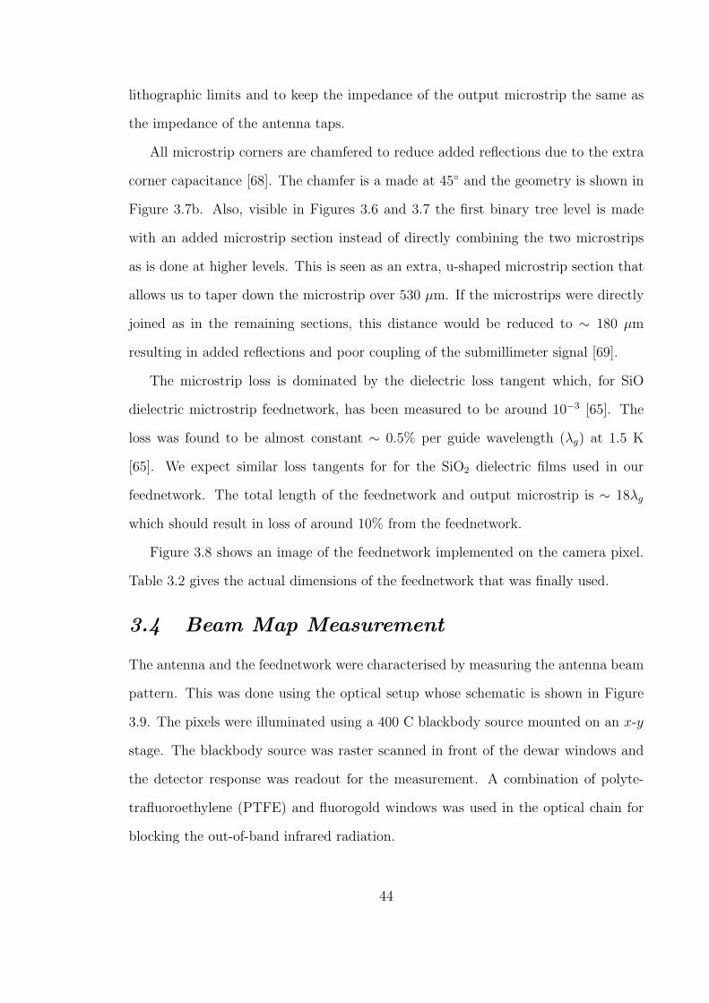
lithographic limits and to keep the impedance of the output microstrip the same as
the impedance of the antenna taps.
All microstrip corners are chamfered to reduce added reflections due to the extra
corner capacitance [68]. The chamfer is a made at 45 and the geometry is shown in
Figure 3.7b. Also, visible in Figures 3.6 and 3.7 the first binary tree level is made
with an added microstrip section instead of directly combining the two microstrips
as is done at higher levels. This is seen as an extra, u-shaped microstrip section that
allows us to taper down the microstrip over 530 µm. If the microstrips were directly
joined as in the remaining sections, this distance would be reduced to ∼ 180 µm
resulting in added reflections and poor coupling of the submillimeter signal [69].
The microstrip loss is dominated by the dielectric loss tangent which, for SiO
dielectric mictrostrip feednetwork, has been measured to be around 10−3 [65]. The
loss was found to be almost constant ∼ 0.5% per guide wavelength (λg) at 1.5 K
[65]. We expect similar loss tangents for for the SiO2 dielectric films used in our
feednetwork. The total length of the feednetwork and output microstrip is ∼ 18λg
which should result in loss of around 10% from the feednetwork.
Figure 3.8 shows an image of the feednetwork implemented on the camera pixel.
Table 3.2 gives the actual dimensions of the feednetwork that was finally used.
3.4 Beam Map Measurement
The antenna and the feednetwork were characterised by measuring the antenna beam
pattern. This was done using the optical setup whose schematic is shown in Figure
3.9. The pixels were illuminated using a 400 C blackbody source mounted on an x-y
stage. The blackbody source was raster scanned in front of the dewar windows and
the detector response was readout for the measurement. A combination of polyte-
trafluoroethylene (PTFE) and fluorogold windows was used in the optical chain for
blocking the out-of-band infrared radiation.
44

Room Temp
1” Zotefoam
1” PTFE
1” PTFE
0.06” Fluorgold
300 K
77 K
4 K
220 mK
400 oC Blackbody
On X-Y stage
13.9
”
Lyotstop
4 K
Detector Chip
PTFE Lens
Figure 3.9: Optical chain used to measure the beam maps
The figure also shows a lens was used in the optical chain. The cryostat used
to measure the beam maps was adapted from an existing setup and had windows
smaller than the beam size. The lens was needed to ensure that the main beam was
not blocked by the dewar winows. This arrangement will reduce the efficiency of
coupling to the telescope optics due to beam mismatch and will be rectified for future
cryostat designs. The lens has a diameter 3.67” and a radius of curvature of 75 mm
for the parabola on both sides. The maximum thickness was 32.45 mm. PTFE has
a refractive index of 1.44. The distance between Lyot stop and the pixel was twice
the lens focal length, such that the location of the antenna beam waist is at the same
location as the Lyot stop. The Lyot stop is a cold surface (4 K) with an aperture in
45

-2
0
2
-2
0
2
0
0.5
1
X (inches)Y (inches)
No
rmal
ised
Res
po
nse
-2 -1 0 1 2-2
-1
0
1
2
X (inches)
Y (
inch
es)
-2 -1 0 1 2-2
-1
0
1
2
X (inches)Y
(in
ches
)
a)
b)
c)
d)
e)
f)
BPF 1 (209 - 265 GHz) BPF 2 (335 - 361 GHz)
−1.5 −1 −0.5 0 0.5 1 1.50
0.1
0.2
0.30.4
0.5
0.60.7
0.80.9
1
Radius (Inches)
No
rmal
ised
Res
po
nse
-2
0
2
-2
0
2
0
0.5
1
X (inches)Y (inches)
No
rmal
ised
Res
po
nse
−1 0 1 2
0.5
0.6
0.7
0.8
0.9
1
Radius (inches)
Norm
alis
ed R
esponse
Figure 3.10: a), b), d), e) show 3D (top) and 2D (bottom) contour maps for theantenna beams. x and y axes show the location on the antenna beam and z axis(color in the 2D map) shows the normalised antenna response at the location. c), f)show ZEMAX simulations for the same. All the plots are at a distance of 13.9” fromthe Lyot stop. The plots in the left column are for the 209-265 GHz band and in theright column are for 335-361 GHz band.
the center, which terminates the antenna diffraction sidelobes but lets the antenna
main beam pass through the aperture.
Figure 3.10 shows the beam maps for the antenna in the two frequency bands (209-
265 GHz, 335-361 GHz). The contour plots are the actual data with the blackbody
source 13.9” away from the Lyot stop. The bottom two plots are the simulations for
46

the same optical configuration as used to take the beam maps using ZEMAX [70]. The
near-field simulations done using ZEMAX result in fringes in the calculated response
which have been smoothed using a box car function. Residues of these smoothed out
fringes are still visible as, for example, the dip at the center of the 335-361 GHz band
(Figure 3.10 f)). However, the beams are seen to be well defined with sharp skirts.
The measured FWHM value of the beam matches the ZEMAX simulations well, with
a beam diameter of 2.45” (2θout = 10).
We notice a slight dip at the center of the beam for the first BPF band (209-265
GHz) and a small hump for the second BPF band (335-361 GHz) in the measured
response. These features may be a result of making the beam map measurements in
the near field. The far field is 40” away and at that distance a 400 C blackbody gives
a poor signal-to-noise ratio, which results in poor quality beam maps. A stronger
source (1000 C) will be used in the far field for further studies. But the results for
simulations and measured beam maps are seen to be in good agreement, and the
quality of beam maps was good enough to use the pixel for first demonstration of the
camera on the sky (Chapter 5).
3.5 Photon Detector Design
The photon detectors used to detect the submillimeter wave signal were implemented
using Kinetic Inductance Detector (KIDs) technology [27] developed in our group at
Caltech and JPL. This section outline the physics and operating principles of these
devices.
3.5.1 Physics of Microwave Kinetic Inductance Detectors
KIDs are pair-breaking, superconducting photon detectors. Electrons in the ground
state of a superconductor are bound together to form Cooper pairs. This results in an
energy gap in the electronic density of states, similar to semiconductors. The energy
gap is typically a couple of meV and falls in the submillimeter frequency range. The
47

table 3.3 lists the values for some typical superconductors. When photons with energy
higher than the Cooper pair binding energy (2∆) are absorbed in a superconductor,
the Cooper pairs are broken resulting in the formation of single electron quasi-particles
(Figure 3.11). This quasi-particle density perturbation causes a measurable change
in the surface impedance of the superconductor, which can be used to make a photon
detector.
Figure 3.11: Schematic to explain Cooper Pair breaking in superconductors due tophoton absorption. Cooper pairs at the Fermi energy break into quasi-particles whenstruck by a photon with energy hν > 2∆.
Figure 3.12 plots the change in surface reactance (δXs), surface resistance (Rs),
and quasi-particle density (nqp) of the superconductor as a function of the temper-
ature. The dependence of the thermal quasi-particle density on temperature can be
Superconductor Energy Gap (meV) Energy Gap (GHz)
Aluminum 0.375 90
Tantalum 1.45 350
Niobium 2.9 700
Table 3.3: Energy gaps of some typical superconductors in meV and GHz
48

Figure 3.12: A plot showing surface resistance, change in surface reactance, andquasi-particle density in aluminum as a function of temperature at 10 GHz (Credit:Prof. Jonas Zmuidzinas)
calculated using:
nqp(T ) = 2N0
√
2πkBT∆(0)e−∆(0)/kBT (3.8)
where N0 is the single spin density of states at the Fermi energy, kB is the Boltzmann’s
constant, ∆(0) is the energy gap at 0 K and T is the temperature. For Aluminum
N0 = 1.72 × 10¹⁰/eV/µm3 including the electron-phonon enhancement factor [27].
The surface impedance change with temperature can be calculated using the
Mattis-Bardeen theory [55]. The figure shows that the δXs, Rs and nqp, all de-
crease exponentially with the temperature which indicates that the responsivity of
the detector remains constant so long as it is operated well below critical temperature
of the superconductor. This can shown more rigorously as follows. The response of
the superconductor to pair breaking submillimeter radiation may be quantified by
change in surface impedance per change in quasi-particle density as:
49

Rnqp =δLs
δnqp
(3.9)
For thin films the fractional change in surface inductance depends on fraction change
in imaginary part of conductivity (σ2) as:
δLs
Ls
= −δσ2
σ2
(3.10)
Rnqp can then be written as:
Rnqp = −Ls
σ2
δσ2
δnqp
(3.11)
Using Mattis-Bardeen theory we have, assuming temperature much lower than su-
perconductor’s transition temperature:
δσ2
δnqp
= − σ2
2N0∆(0)
(
1 +
√
2∆(0)
π2~ω
)
(3.12)
Using Ls =1
σ2t, for thin films, t being the film thickness, we get the final expression
for Rnqp as:
Rnqp =δLs
δnqp
=1
2N0∆(0)σ2t
(
1 +
√
2∆(0)
π2~ω
)
(3.13)
which is nearly independent of the temperature so long as the film is well below its
superconducting transition temperature implying the same for the responsivity of the
photon detector.
Small changes in Zs of the superconductor (e.g., Al) can be sensitively measured
by fabricating a transmission line resonantor out of it. The transmission line resonator
is made using the coplanar waveguide geometry similar to that discussed in Chapter 2
and are readout using a similar homodyne measurement scheme. The ideal resonator
response is given by (Figure 3.13):
50

S21(δx) =
[
1 − Qr
Qc
1
1 + 2jQrδx
]
(3.14)
where δx =f − fr
fr
, where f is the microwave readout frequency and fr is the reso-
nance frequency, Qr and Qc are the resonator total quality factor and coupling quality
factor, respectively.
1
cQ
Q−1
Re
Im S21
a) b)
0.2
0.4
0.6
0.8
1
30
60
90
330
0
Figure 3.13: a) Polar plot of S21 data (thick blue line) and the fit (thin green line).The resonator has a resonance fr = 5.334 GHz and Qr = 9866. b) A schematic ofthe S21 plotted in complex plane
The magnitude of the complex response is seen as a dip in the microwave forward
scattering parameter (S21) at the resonance frequency (Figure 3.14). The figure also
shows change in the response of the resonator as it is exposed to the submillimeter
radiation of increasing intensity. The submillimeter radiation for this experiment was
generated using a blackbody source whose temperature can be varied from 4 to 20 K
in steps of 2 K. As the temperature of blackbody is changed the resonance frequency
of the device changes by approximately 30 KHz for every 2 K change in blackbody
temperature. The total change in the device resonance frequency and quality factor
is 300 KHz and 1400 over the temperature sweep range starting with initial values
51

of 5.334 GHz and 9866, a fractional change of 5.6×10⁻⁵ and 0.1419, respectively.
This happens due to the increase in surface impedance and quasi-particle number
consistent with the trend in Figure 3.12. The total bandwidth of the resonator is
close to 500 KHz and the above changes in Qr and fr are easily discernible.
The responsivity of the resonator can then be calculated as change in S21 per
change in submillimeter power (Popt) and can be written as:
R =δS21
δx
δx
δLs
δLs
δnqp
δnqp
δPopt
(3.15)
whereδLs
δnqp
is given by equation 3.13 andδnqp
δPopt
defines the efficiency of the optical
chain. Differentiating equation 3.14 we have
dS21
dδx=Q2
r
Qc
[
d(1/Qr)
dδx+ 2j
]
(3.16)
The total quality factor of the resonator is given by the usual formula 1/Qr = 1/Qc +
1/Qi where the power lost to the outside world through the coupler limits Qc and
the resonator internal losses limit Qi (See Table 3.4). The expression for Qr is Qr =
QcQi
Qc +Qi
and the responsivity scales as R ∼ QcQ2i
(Qc +Qi)2which for small values of Qc
scales as R ∼ Qc and for large values of Qc scales as R ∼ 1/Qc. It is easily shown
that the responsivity maxima occurs at Qc = Qi by checking for the extremum of
Q2r/Qc with respect to Qc where Qi is the internal quality factor of the resonator
under loaded conditions (See Table 3.4). The differential term inside the brackett
in equation 3.16 is the change in the Qr with the change in fr due to change in the
quasi-particle density due to the photon absorption and can be calculated using the
Mattis-Bardeen theory.
3.5.2 Resonator Design
Figure 3.15 shows the photon detector. A hybrid design is used for the resonator
where most of the coplanar waveguide is made using niobium superconductor but the
52

0.2
0.4
0.6
0.8
1
30
0
Phase
(Deg)Mag.
a) b)
5.332 5.333 5.334 5.335 5.336
0.5
0.6
0.7
0.8
0.9
1
Frequency (GHz)
Tra
nsm
issi
on S
21
∆f = -300 kHzQ = −1400
Figure 3.14: The forward transmission |S21| with change in submillimeter signalpower. a) shows the change in magnitude of the response while b) plots the responsechange in the complex plane (similar to Figure 2.5). Blue lines and dots show thechange in the complex response at a constant readout frequency. The measurementwas performed using the circuit shown in Figure 2.4. As the submillimeter poweris increased by raising the illuminating blackbody temperature from 4 to 20 K thecurves are shown in color changing from black to red. The data shown is for a hybridresonator (see Section 3.5.2) made using a 20 nm thick film of aluminum on sapphiresubstrate. The total length of the resonator is 3.5 mm
Mechanism Approx.Q
Substrate loss 1,000,000
CPW radia!on 1,000,000
Submm Microstrip Coupling 100,000
300 K Op!cal loading 15,000
Coupler length (150 μm on Si) 15,000
Table 3.4: Table for effects limiting resonator Q
sensitive short-circuited end of the resonator where the photons are absorbed is made
out aluminum. Thickness of the niobium film is 2000 A while that of aluminum
53

input output
Lc
Feedline
Niobium
Ground Plane
Niobium
Center Strip
Aluminum
Sensor
Center Strip
Figure 3.15: Schematic of a hybrid coplanar waveguide resonator used as a photondetector
Microstrip
Wiring
CPW Slots
Niobium
Plug/GroundCPW Center
Conductorb)
a)
Figure 3.16: a) Picture of the submillimeter coupling section of the MKIDs withmicrostrip from the bandpass filter running over the aluminum part of CPW centerstrip. b) Schematic close up (not to scale) of submillimeter coupling end of theMKIDs. niobium ground plane is shown in blue. Aluminum layer is shown in orange,while the niobium wiring layer is shown in grey
54

Geometry
(Center-Slot)
(µm)
Coupling
Constant
(µm/GHz)2
6-4 3.5x10¹⁰
6-3 3.57x10¹⁰
6-2 3.79x10¹⁰
7-1 4.55x10¹⁰
5-0.5 5.67x10¹⁰
5-1 6.6x10¹⁰
Table 3.5: Table for coupling strength for different CPW geometries
film is 200 A. This design is necessary since making the entire coplanar waveguide
using aluminum would cause the sub-mm radiation to couple to the resonator directly
instead of through the antenna, feed network and bandpass filter channel since the
thin aluminum film impedance matches the free space impedance well. This design
also allows us to separate the two functionalities of photon absorption and detection
in to two separate parts of the resonator allowing more freedom for design.
In addition to the coplanar waveguide geometry (i.e., the center conductor width
and the slot spacing), the resonator design is completely specified by its resonance
frequency, coupling quality factor, and length of the aluminum section. The total
length of the resonator determines its resonance frequency. The resonator Q may
be limited by multiple effects listed in Figure 3.4. We empirically know that the
best substrates have given us internal Qs of close to 1 million. Coplanar waveguide
radiative losses limit Qs to about the same order of magnitude [71], depending on the
geomtery. Q limitations due to coupling to the submillimeter circuit can be estimated
using SUPERMIX to be close to a 100,000. Calculations show, however, [72] that
optical loading due to 300 K atmospheric emission will limit the Q to about 15,000.
The coupling quality factor governed by the coupler length should match this value
for maximum responsivity.
55

3.5.2.1 Total Length
Once the resonance frequency of the resonator has been specified the length of the
resonator can be calculated using:
L =c
4fr√εeff
(3.17)
where c is the speed of light and εeff is the effective dielectric constant seen by the
electro-magnetic wave travelling in the CPW and ideally includes effects of super-
conductivity as well [57]. εeff can be estimated as εeff = (εd + 1)/2 where εd is the
substrate dielectric constant.
3.5.2.2 Coupler Length
The coupler length can be ascertained by calculating the coupling capacitance between
the feedline and coupling section of the resonator. The feedline geometery used was
10 µm center strip and 6 µm slots. The resonators used had a center strip of 6 µm and
2 µm slot width. Both the co-planar waveguides were separated by a 2 µm ground
plane. In order to calculate the resonator Qc the feedline and coupling section of the
resonator can be simulated as a 3-port network (Figure 3.17) with coupling between
port 1 and 3 defined by scattering parameter S31 related to the resonator Qc as:
Qc =π
2 |S31|2. (3.18)
Using the layout shown in Figure 3.17 the 3-port network may be simulated using
SONNET to calculate the scattering parameter for different coupler lengths (Lc) and
fr. Assuming a linear dependence of transmission parameter S31 on fr and Lc, which
physically corresponds to a capacitive coupling between the resonator and the feedline
it can be written as [73]:
S31 = AfrLc +Bfr + CLc +D. (3.19)
56

1 2
3
S12
S23
S31
Figure 3.17: Three port network with ports 1 and 2 feedline input and output portsand port 3 the end of coupling section of the resonator
The data is fitted to the model in equation 3.19 to extract parameters A, B, C,
and D [73]. Since the coupling is primarily capacitive for our design (Chapter 5),
AfrLc >> Bfr, CLc, D. Lc for a given Qc can then be calculated using:
Lc(µm) =1
fr(GHz)
√
A
Qc
. (3.20)
Values for A are tabulated for different CPW geometries in Figure 3.5. Using these
values and resonance frequency in GHz gives coupler lengths in µm.
3.5.2.3 Resonator-microstrip Submillimeter Overlap
The submillimeter radiation is coupled to the resonator by running the microstrip
line over the CPW center strip as shown in Figure 3.16. The bottom layer for the
microstrip is made using the aluminum part of CPW while the top layer remains nio-
bium, with SiO2 dielectric in between. The length of the aluminum section is decided
by the length of overlap required to dump most of the submillimeter power from the
57

Device Parameters Inputs
Frequency (GHz) 200
Temperature (K) 0.22
Characteristic Impedance (Ω) 24
Niobium Film Parameters Inputs
Gap Voltage (mV) 2.9
Critical Temperature (K) 9.2
Resistivity (µΩ-cm) 2.5
Thickness (A) 2000
Aluminum Film Parameters Inputs
Resistivity (µΩ-cm) 2.82
Thickness (A) 200
SiO2 Dielectric Parameters Inputs
Dielectric Constant 4
Loss Tangent 0.0001
Microstrip Properties Outputs
Characteristic Impedance (Ω) 27.81
Propagation Constant (/mm) 5.03+j 9.6
Power Fraction Absorbed
Outputs
Length
(mm)
0.9 0.297
0.95 0.368
0.99 0.53
0.999 0.76
Table 3.6: Design parameters for the submillimeter coupler
microstrip to the CPW. This was calculated using SUPERMIX, and the length of
CPW and microstrip overlap required to dump close to 100% of the submillimeter
power at 200 GHz was determined to be 1 mm. The table 3.6 shows the parameter
values used for the SUPERMIX simulations and the corresponding outputs.
Making the submillimeter coupling section long will result in microwave (4-12
58

GHz) readout signal to leak out from the coupler and lower the quality factor of the
resonator, but for the low coupling quality factors close to 15,000 used in our designs
this is not a major issue.
Also it is essential that the section of aluminum under the ground plane and the
CPW resonator be electrically connected using niobium and not aluminum to prevent
the quasi-particles in the center strip from escaping into the ground and lowering the
response of the device. The details of the ’niobium plug’ which prevents this from
happening are as shown in Figure 3.16b.
3.6 Fabrication Steps
Substrate
(Si/Sapphire)
Microstrip
layer Antenna
Aluminum
Sensor Layer
Niobium Ground
Plane
SiO2
Figure 3.18: Schematic of pixel showing the various layers required for pixel fabri-cation
Figure 3.18 shows the various layers of material used to fabricate the pixel. The
aluminum sensor layer is first deposited on the silicon (or sapphire) substrate using
DC magnetron sputtering. The sensor layer is then patterned using photoresist and
BCl3/Cl2 inductively coupled plasma (ICP) etching. The niobium ground plane is
deposited using DC magnetron sputtering. The ground plane is patterned using
59

photoresist and SF6 ICP etching. SiO2 is deposited by RF magnetron sputtering
with a substrate bias. The vias on the niobium ground plane are patterned using
photoresist and CHF3/O2 ICP etching. The wiring layer of the niobium microstrip
is deposited using DC magnetron sputtering and is patterned using BCl3/Cl2 ICP
etching. The dielectric is removed using photoresist and CHF3/O2 ICP etching.
Finally, CPW is patterned using photoresist and BCl3/Cl2 ICP etching.
3.7 Conclusions
We have designed and tested various components necessary to implement a submil-
limeter pixel on chip. The antenna was implemented using a multi-slot structure on
chip. The antenna has a narrow beam and does not require any extra on-chip optics to
couple the light from the telescope. The submillimeter power from the antenna slots
is combined using binary tree feednetwork which brings it out into a single output
microstrip which then passes it through inline BPFs (see Chapter 4). The antenna
and the microstrip were implemented using niobium and SiO2 dielectric. The photon
detectors were implemented using microwave kinetic inductance detectors. The sub-
millimeter power is coupled from the output microstrip to the detector by running
the microstrip over the shorted end of MKIDs made out of aluminum. The detector
response is measured as change in the transmitted readout microwave signal using a
through line capacitively coupled to the resonator. The complete layout of the single
pixel schematic is shown in Figure 3.19. Figure 3.20 shows a photograph of an actual
pixel taken using the optical microscope.
60

Nb resonator , with shorted end made from Al
(Photon Detector)
Multi-slot antenna,
Binary tree networkBandpass Filters
Figure 3.19: Schematic of the final pixel with all the sub-components put together.It shows 8 slots and 8 taps on each slot making up the antenna for clarity, the actualnumber is 16 for both (Figure 3.20).
61

Nb resonator , with shorted end made
from Al (Photon Detector)
Bandpass Filters Multi-slot antenna,
Binary tree network
Figure 3.20: Picture of the two-color pixel taken under an optical microscope
62

CHAPTER IV
BANDPASS FILTER DESIGN
4.1 Introduction
100 200 300 400 500
0.2
0.4
0.6
0.8
Frequency (GHz)
Tra
nsm
issi
on
Water lines
Passbands
Figure 4.1: Atmospheric transmission spectrum (solid line) at CSO overlaid on theideal filter responses (dotted lines) calculated using the inductor and capacitor valuesgiven in Table 4.1. The atmospheric spectrum was generated using the programatm cso [74] (http://www.submillimeter.caltech.edu/cso/weather/atplot.shtml).
The opacity of the Earth’s atmosphere obscures portions of the sub-THz sky to
ground-based astronomical observation. This requires that band-defining filters be
used in conjunction with broad-band antenna and detectors to construct pixels work-
ing at mm-submillimeter wavelengths to reduce the loading on the detectors from the
Earth’s atmosphere. This chapter presents the design and testing of superconducting,
lumped-element, on-chip bandpass filters (BPFs), placed inline with the microstrip
63

connecting the antenna and the detector, covering the frequency range from 209-416
GHz. Four filters (BPF 1, 2, 3, and 4) were designed with passbands of 209-265 GHz,
274-315 GHz, 335-361 GHz and 397-416 GHz, corresponding to the atmospheric trans-
mission windows shown in Figure 4.1. The first atmospheric window extends from
200-320 GHz and is divided into two roughly equal parts by BPFs 1 and 2. Fourier
transform spectroscopy (FTS) was used to verify that the spectral response of the
BPFs is well predicted by the computer simulations. Two-color operation of the
pixels was demonstrated by connecting two detectors to a single broadband antenna
through two BPFs. A new pixel design allowing four-color operation is also discussed.
There are various existing designs for defining the passbands of mm-submillimeter-
wave pixels. Metal-mesh filters [64] have been used in conjunction with IR block-
ing materials such as teflon and fluorogold to make quasi-optical filters that can be
mounted on the dewar windows or device box. This approach, however, has the disad-
vantage of preventing multi-color pixel operation, since the entire array is irradiated
by the same frequency band. Multi-color pixel operation is desirable for upcoming
camera designs [75] to increase the overall throughput for a wide field survey by cap-
turing more photons in different frequency bands. This has many advantages, as
listed in Chapter 1, and additionally uses the focal plane more efficiently. Further,
the quasi-optical mesh filters are optimally designed for normally incident radiation.
Obliquely incident radation may leak through and load the detector. Since these
filters are mounted on the dewar windows they need to be carefully heat sunk to
prevent detector loading due to radiation emitted by the filters themselves. Multiple
filters and IR blockers in the optical chain also need to be coated with anti-reflection
(AR) films to prevent non-uniform transmission as a function of frequency in the filter
passband, due to standing waves present because of the refractive index mismatch at
the interfaces of adjacent optical components.
Although we chose to use lumped-element designs, on-chip bandpass filters may
64

also be implemented using distributed circuit elements [39]. However, using dis-
tributed circuit elements causes the bandpass filters to leak at higher harmonic fre-
quencies requiring a cascaded lowpass filter. This adds to the complexity of the
circuit and takes up precious real estate on the chip. The lowpass filter may also be
implemented using a metal mesh filter again leading to some of the issues mentioned
above.
The lumped-element, on-chip bandpass filters presented in this chapter circumvent
all the above problems.
4.2 Bandpass Filter Design
4.2.1 Lumped–Element Circuit Design
L1
C1
L1
C1
C2
L2
Lser
Cser1
Lser
Cser2
Cshunt
Cshunt
Lser
Cser1
a) b)
d)L
1C
1c) L1
C1
L1
C’2
Cn
Ln
Ln
K
-C -C
C
-C -C
C
K
Figure 4.2: Steps for lumped-element bandpass filter circuit design: a) 3-pole But-terworth low-pass filter prototype. Ln and Cn are normalised inductor and capacitor,respectively. b) Bandpass filter with series LC and shunt parallel LC resulting fromthe prototype low-pass filter. c) Bandpass filter with impedance inverter blocks andno shunt inductors. d) Final lumped-element bandpass filter circuit with no shuntinductors
We use a three-element Butterworth lowpass filter prototype (Figure 4.2a) with
cutoff at ωc = 1 and terminated in a 1 Ω load as a basis for design of our bandpass
filters. Using a Butterworth prototype should minimise any ripples in the filter pass
or stop bands. This normalised lowpass filter has element values Ln = 1, Cn = 2
65

Element
values
BPF1
209–265
GHz
BPF2
274–315
GHz
BPF3
335–361
GHz
BPF4
395–416
GHz
Lser (pH) 75 123.2 146.91 201.04
Cser1 (fF) 7.37 2.48 1.50 0.79
Cser2 (fF) 9.01 2.69 1.59 0.82
Cshunt (fF) 40.23 31.36 26.97 23.1
Table 4.1: Circuit element values for Figure 4.2 d) for the BPFs corresponding tothe atmospheric transmission windows
(Figure 4.2a). It is converted to a lumped-element bandpass filter using the usual
transformations [68], and replacing the series inductor by a series combination of
inductor (L1 =Z0Ln
ω0∆) and capacitor (C1 =
∆
Z0Lnω0
), and shunt capacitor by a
parallel combination of inductor (L2 =Z0∆
Cnω0
) and capacitor (C2 =Cn
Z0∆ω0
) (Figure
4.2b). Z0 is the embedding impedance set by the characteristic impedance of the
microstrip transmission line which brings submillimeter power from the antenna and is
equal to 20 Ω. ∆ (= ωc2−ωc1) is the design bandwidth of the BPF and ω0 (=√ωc1ωc2)
is the center frequency of the BPF given by the geometric mean of the 3 dB cutoff
frequencies of the BPF. ωc1 and ωc2 are the upper and lower cutoff frequencies of the
bandpass filter, respectively.
For the ease of fabrication of the circuit it cannot have any shunt inductors to
ground. For sufficiently narrow bandwidth (10−20%) impedance inverters can be used
to replace a parallel shunt admittance (Yp) by a series impedance (Zs) for two-port
networks [76] (Figure 4.2c). Using the identity Zs = K2Yp, where Zs = jωL1 +1
jωC ′2
,
Yp = jωC2 +1
jωL2
, and K is the impedance inverter, we get the value for K and
series capacitance K2 = L1/C2 and C ′2 = L2C2/L1.
The impedance invertor is implemented using a two-port T network with the series
66

branches containing capacitors −C and shunt branch containing capacitor C where
C = 1/ω0K (Figure 4.2c). The negative capacitance in the series branches can be
absorbed into C1 and C ′2 to give the final circuit (Figure 4.2d). Here Lser = L1,
Cshunt = C, Cser1 =CC1
C − C1
, and Cser2 =CC ′
2
C − 2C ′2
.
The lumped circuit element values are then further optimised using HP-ADS [77],
a circuit simulation software package, to give a power transmission of at most 10−4
in stop band, unity transmission in passband with sharpest possible rolloff. These
optimised values for various lumped components for the four bandpass filters are
listed in Table 4.1.
4.2.2 Circuit Layout and Fabrication
The schematic of the filter layout is shown in Figure 4.3. The integrated inline BPF
circuit was fabricated on chip with the other pixel components using photolithography.
The inductors were implemented using spiral geometry and the capacitors in the
parallel plate configuration. The bottom layer is 200 nm thick niobium film deposited
on the silicon substrate using DC magnetron sputtering. The ground plane, spiral
inductors (Figure 4.3 shown in blue) and lower plate of the parallel plate capacitors
(not visible in Figure 4.3) are patterned on this layer using photoresist and SF6
Inductively Coupled Plasma (ICP) etching. Following this, a 400 nm thick SiO2
dielectric layer is deposited on the bottom layer by RF magnetron sputtering with
substrate bias. Subsequently, a 200 nm thick layer of niobium is deposited using DC
magnetron sputtering and patterned using BCl3/Cl2 ICP etch to form the wiring layer
of microstrip geometry (Figure 4.3, shown in pink). The dielectric is then removed
using a CHF3/O2 ICP etch.
The input microstrip brings the broadband submillimeter power from the slot
antenna to the filter (Figure 3.20). In order to avoid making a via between the
bottom niobium layer and the top, the first series capacitor is divided into two series
67

capacitors each having double the design capacitance (CLSer1 = 2 Cser1) and placed on
either side of the spiral inductor as shown in Figure 4.3a. The microstrip line connects
the second series capacitor to the shunt capacitor. This design is then repeated for
the remaining two series capacitor-inductor sections. Finally, the output microstrip
takes the band limited submillimeter power to the detector.
Nb Ground
Plane
Si Substrate
(Ground Plane
Hole)
Series
Capacitor
(C = 2 C )
Series Inductor
L
Shunt
Capacitor
C
Silicon
Nb Wiring layer
(200 nm)
SiO2 (400 nm)Nb Ground Plane
(200 nm)
a)
b)
Output
MicrostripInput
Microstrip
LSer1 Ser1
1
Series Inductor
L2 s
Shunt
Capacitor
Cs
Series Inductor
L1
Series
Capacitor
(C = 2 C )LSer2 Ser2
Series
Capacitor
(C = 2 C )LSer1 Ser1
Figure 4.3: SONNET layout for the bandpass filters: (a) top view, b) side view.The top microstrip is made of niobium (pink). Below it is a layer of SiO2 (grey, notvisible in the top view), then niobium ground plane (blue). The series inductors andcapacitors are fabricated on top of the sapphire substrate (white) directly in holes inthe ground plane.
68

R1
R2
Rn
din
dout
t
Figure 4.4: Spiral inductor schematic detailing the dimensions used in the inductordesign. Rn is the length of the nth arm of the spiral inductor with n = 1 for theoutermost arm. dout and din are the outermost and innermost dimension of theinductor, respectively. t is the trace width.
4.2.3 Component Design
4.2.3.1 Spiral Inductor Design
Correct design of the inductor is critical for the optimal performance of the bandpass
filter. The inductor may either be implemented using the CPW geometry which is
simpler to layout but can provide relatively smaller inductance values, or a spiral
geometry, which was finally used for our design. To make the design choice we
calculated the length of CPW required to provide the minimum required inductance
of 75 pH, as follows.
Let Z0 (= 20 Ω), Zc (= 50 Ω), εd (= 10.5), f (= 250 GHz) be the characteristic
embedding impedance of the external circuit, characterstic impedance of CPW used
to implement the lumped inductor, substrate (sapphire) dielectric constant and the
filter center frequency, respectively. The effective dielectric constant seen by the EM
wave is close to εeff = (εd + 1)/2 = 5.75. This may be calculated more accurately
using SONNET simulations.
Using equations for transmission line characteristic impedance and propagation
69

BPF 1 BPF 2 BPF 3 BPF 4
L1 L2 L1 L2 L1 L2 L1 L2
R1 3.5 2.5 5.5 5 7 7 7.5 7.5
R2 19.5 20 17.5 17.5 15.5 15.5 15.5 15.5
R3 21 21 21 21 17 17 16.5 16
R4 12 10 14.5 14.5 12.5 12.5 12.5 12.5
R5 4.5 2.5 8 8.5 13 13 12.5 12
R6 0 0 2.5 2.5 5 5.5 9.5 9.5
R7 0 0 0 0 3 3 8 8
R8 0 0 0 0 0 0 3.5 3
t 1 1 1 1 1 1 1 1
Table 4.2: Spiral inductor dimensions for all the bandpass filters with schematicshown in Figure 4.4. L1 and L2 are shown in the SONNET layout for the BPF, inFigure 4.3a. The values for L1 and L2 are nominally equal (Table 4.1) and theirdimensions are close to each other. However, they end up with slightly differentdimensions while tweaking the layout in SONNET due to the small difference ingeometry of the capacitors CLSer1 and CLSer2. All the dimensions are in microns.
constant we can get the inductance per unit length:
Zc =
√
LC , β = ω
√LC (4.1)
L =βZc
ω=
√εeffZc
c(4.2)
where L, C are inductance and capacitance per unit length, c is the speed of light, β
is the propagation constant, and ω is the frequency in radians/sec. The wavelength
of the EM wave in sapphire at 250 GHz is 500 µm. Using equation (4.2) the length
of CPW line required to implement inductance (L = 75) pH lumped inductor is
l =Lc
√εeffZc
= 187.67 µm, which is a significant fraction of the wavelength. Hence,
a 75 pH inductor implemented using CPW with the above Zc will behave like a
distributed element. This will cause the filter to leak at integral multiples of the
transmission line fundamental mode.
70

Following [76] we can calculate the maximum inductance we can extract from
CPW geometry with the above characteristic impedance at frequencies of interest
(≃ 250 GHz) for a given error, as follows: The input impedance for the lumped
element is given by:
Zin = ZcZ0 + jZct
Zc + jZ0t(4.3)
where t = tan(βl). Since we want to use sections of CPW much shorter than the
wavelength and use high characteristic impedance sections to emulate inductors we
can use the approximation Z20 t
2 << Z2c . This gives us:
Zin = Z0 + Z0t2
(
1 − Z20
Z2c
)
+ jZct
(
1 − Z20
Z2c
)
. (4.4)
Comparing the real and imaginary parts of equation (4.4) to expression for input
impedance of ideal lumped inductor Zin = Z0 + jXl we get Xl = Zct(
1 − Z2
0
Z2c
)
.
To have the real part of the impedance match closely with the ideal case we need
t2(
1 − Z2
0
Z2c
)
→ 0. Assuming, a 5% error in real part of the imepdance (i.e., t2(
1 − Z2
0
Z2c
)
=
0.05) we get βl = 0.26. Using equation (4.2) we get maximum value for lumped-
element inductance using this scheme L = 8.28 pH, which is much less than the value
needed.
A spiral geometry for the inductor can instead be used to provide the high values
of the inductance needed for the bandpass filters. The rectangular spiral (Figure 4.4)
was chosen for layout convenience and the geometry was guessed by calculating the
inductance using the formulae available in the literature [78]:
L =µn2davgc1
2(ln(c2/ρ) + c3ρ+ c4ρ
2) (4.5)
ρ =dout − din
dout + din
(4.6)
davg =dout + din
2(4.7)
71

Here L is the inductance and c1, c2, c3, and c4 are geometry dependent co-efficients
with values 1.27, 2.07, 0.18, and 0.13, respectively, for rectangular spiral geometry. ρ
is the filling fraction, with din and dout the innermost and the outermost dimensions
of the inductor (Figure 4.4), µ is the magnetic permeability, and n is the number of
turns. This formula is not very accurate for large values of s/w where s is spacing
between the traces and w is the trace width, but exhibits maximum error of ∼ 8%
when s ≤ 3w for regular spirals [78]. s is typically 2-4 µm, while w is 1 µm, and the
formula works well as a zeroth order approximation since, in the final design, the s
changes from one turn to the next. The final inductor geometry is obtained by laying
it out in SONNET [79], simulating its impedance, and re-optimising the geometry
to give the desired inductance value. The optimization is done keeping in mind the
trends that decreasing the spacing between adjacent traces increases their coupling
and hence the mutual inductance, and vice versa, and that the orthogonal traces are
decoupled from one another. The trends suggested by the formulae in equation (4.5),
such as dependence on the number of turns are also used. The exact final dimensions
of each of the inductors finally used to implement the BPFs are tabulated in Table
4.2.
4.2.3.2 Capacitor Design
The dimensions for the capacitor with capacitance values tabulated in Table 4.1 can
be estimated using parallel plate formula C = ε0εdA/d, where ε0 is the free space
permittivity, εd (= 4) is the dielectric constant of SiO2, A is area of the parallel
plates, and d is the thickness of SiO2 (which is same as distance between the plates).
The capacitor dimensions were further optimised by laying out capacitor-inductor
series combinations in SONNET and optimizing the dimensions of the layout so that
it has a resonance at the same frequency as the series combination of lumped LC with
values in the table 4.1.
72

The final dimensions of the capacitors for each of the filters are tabulated in Table
4.3. As can be seen, the values calculated using the parallel plate formula can be
significantly different from the values finally obtained through simulations.
BPF 1 BPF 2 BPF 3 BPF 4
CLser1 CLser2 Cshunt CLser1 CLser2 Cshunt CLser1 CLser2 Cshunt CLser1 CLser2 Cshunt
Length 11.5 14.5 10.5 8 5 10.5 7 4.5 11.5 3.5 4.5 10
Width 13 15 23 9 7.5 19.5 6 7.5 17.5 5 5 10
Table 4.3: Dimensions of the capacitors in Figure 4.3a in microns assuming a 4000A thick SiO2 dielectric (εd = 4). The actual capacitance value of these capacitorsCLSer1,2 = 2CSer1,2, since two equal value series capacitors are being used to imple-ment the series capacitor shown in circuit schematic Figure 4.2d. The dimensionsof the parallel plate capacitors used to implement first and third series capacitor inFigure 4.2d are exactly the same. Length direction is assumed to be the direction ofpropagation of submillimeter radiation.
4.2.3.3 SONNET Simulations
The response of each of the circuit elements, and subsequently the entire layout, was
simulated using SONNET [79] – a planar 3D electromagnetic simulator. The soft-
ware uses method of moments calculation to compute the response of the circuit.
The SONNET layout of the BPF is seen in Figure 4.3. Initial simulations assumed
the niobium ground plane and wiring layers (seen in blue and pink respectively) to
be perfectly conducting 2D sheets (zero thickness) with 400 nm SiO2 dielectric be-
tween them. The lumped-element geometries were optimised to produce the required
bandpass filter response.
4.2.4 Effect of Superconductivity on the Filter Response
Niobium is used to fabricate the bandpass filters superconducts at the detector op-
erating temperatures (niobium Tc = 9.2 K, Top = 220 mK). Superconductors have a
73

Zn=377Ω
Zx Zx
L = µ0t
Ei
Er
Et
Zx Zx
t
Ei
Er
Et
ZS
t
a) b)
c)
Zn
Zin = ZS
ZnZnZnZn
Figure 4.5: a) A superconducting film of thickness t with surface impedance Zs. Zη
is the free space impedance, Ei, Er, and Et are the incident, reflected, and transmit-ted waves, respectively. b) A SONNET analog for schematic a)–two planar sheetsseparated by distance t having surface impedance Zx where Zx is related to Zs byequation 4.9. c) Equivalent transmission line circuit for the schematics
finite surface impedance at microwave and submillimeter wavelengths [55], and simu-
lating them as 2D planar films of perfect conductors can lead to significant errors in
the bandpass filter response calculation.
SONNET can be used to accurately simulate the bandpass filter response by
incorporating the effects of superconductivity and finite conductor thickness. This
can be done by replacing a single perfectly conducting planar sheet with multiple
planar sheets of a given surface impedance (Zx), different from the the actual surface
impedance (Zs) of the superconducting film, as a model for thick superconducting
film [65, 80]. For λL ≃ t a two-sheet model is sufficient (Figure 4.5a,b) [80].
In the local limit, at temperature well below Tc and frequency well below the
gap frequency, assuming Zη(= 377Ω) >> ωµ0λL(= 0.14 Ω) where Zη is the free
space impedance, and µ0 is free space permeability, the surface impedance of the
74

superconductor is given by [80]:
Zs = jωµ0λL coth(t/λL). (4.8)
The impedance seen by a TEM mode travelling along a transmission line is the same
as the surface impedance seen by an EM wave normally incident upon a conductor
[81]. Using this, the resulting equivalent circuit for the SONNET model in Figure
4.5b is shown in Figure 4.5c. If the distance between the sheets is much smaller
than the wavelength of incident light, an inductor with a value of µ0t can be used to
represent the impedance due to magnetic field energy stored between the sheets in
Figure 4.5b.
Equating the input impedance Zin of the transmission line equivalent circuit for
the film is the surface impedance Zs. We can solve for Zx:
Zx = Zs
[
1 − t
2λL coth(t/λL)+
(
1 +t2
4λ2L coth2(t/λL)
)1/2]
. (4.9)
Dividing Zs and Zx by ω gives us a surface inductance (Ls) of 88.5 fH and a modified
surface inductance (Lx) of 0.1166 pH/.
The above changes in geometry and material properties were incorporated in the
SONNET simulations done earlier with single perfectly conducting sheets. The di-
mensions of the bandpass filter layout were re-optimized to give the new corrected
bandpasses (Figure 4.6). The final layout schematic is shown in Figure 4.7, and the
corresponding dimensions are given in Table 4.4. The actual optical image of one of
the bandpass filters (BPF 1) is seen in Figure 4.8.
4.3 Measurements and Results
Figure 4.9 shows the normalised, predicted and measured responses of the bandpass
filters. The measurement was performed using a Fourier Transform Spectrometer
(FTS). Details of the FTS construction are given in [82].
75
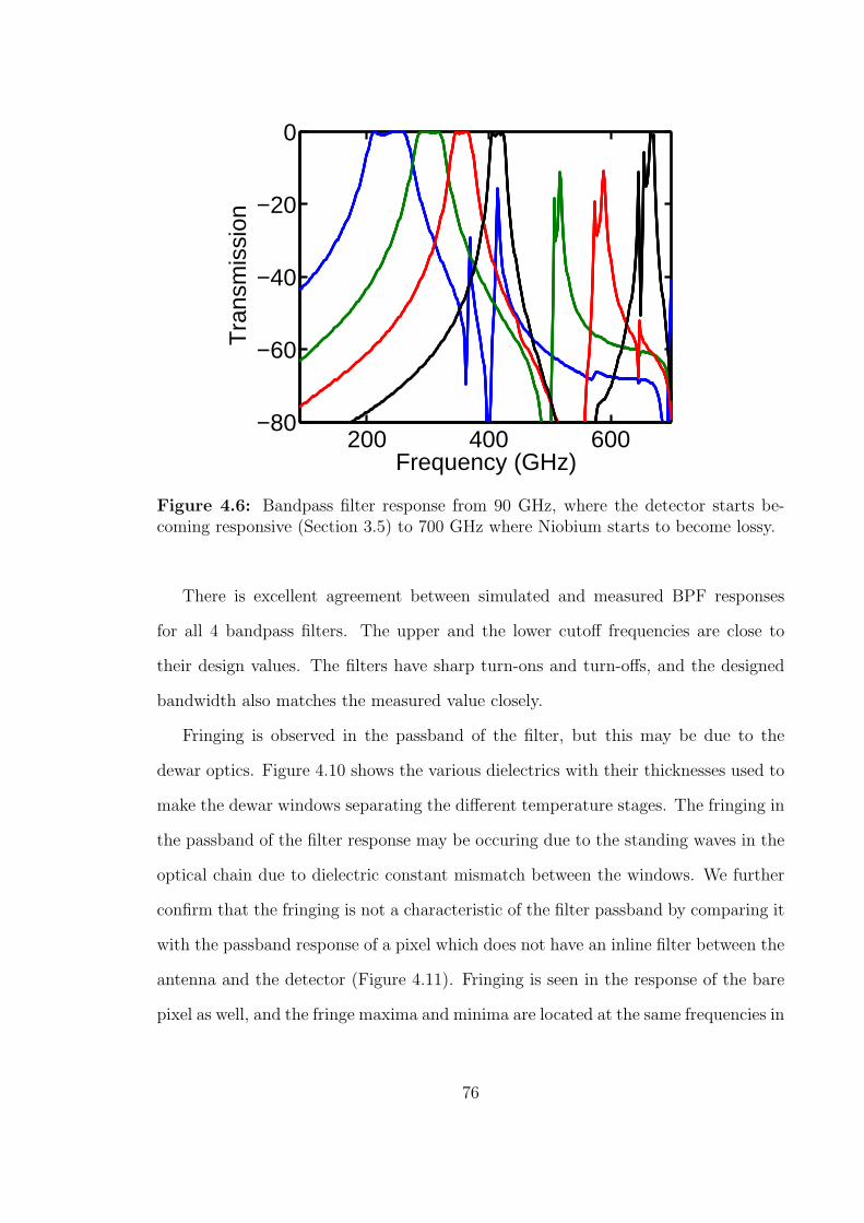
200 400 600−80
−60
−40
−20
0
Frequency (GHz)
Tra
nsm
issi
on
Figure 4.6: Bandpass filter response from 90 GHz, where the detector starts be-coming responsive (Section 3.5) to 700 GHz where Niobium starts to become lossy.
There is excellent agreement between simulated and measured BPF responses
for all 4 bandpass filters. The upper and the lower cutoff frequencies are close to
their design values. The filters have sharp turn-ons and turn-offs, and the designed
bandwidth also matches the measured value closely.
Fringing is observed in the passband of the filter, but this may be due to the
dewar optics. Figure 4.10 shows the various dielectrics with their thicknesses used to
make the dewar windows separating the different temperature stages. The fringing in
the passband of the filter response may be occuring due to the standing waves in the
optical chain due to dielectric constant mismatch between the windows. We further
confirm that the fringing is not a characteristic of the filter passband by comparing it
with the passband response of a pixel which does not have an inline filter between the
antenna and the detector (Figure 4.11). Fringing is seen in the response of the bare
pixel as well, and the fringe maxima and minima are located at the same frequencies in
76

0
1
2 3 4
5 6 7
8 9 10
11 12 13 14 15 16
17 18
19
Figure 4.7: SONNET geometry layout schematic for the final filter. Numbers indi-cate points on the schematic as follows: 0 is the origin, 1 the upper-right corner ofthe layout. 2, 3, 4 and 5, 6, 7 are the lower-left and upper-right corners, respectively,of the holes in the niobium ground plane. 8, 9, 10 are the lower-left corners of thespiral inductor. 11, 12, 13, 14, 15, 16 are the lower-left corners of series capacitorsCLseries1,2,3. 17, 18 are the lower-left corners of the two shunt capacitors. 19 is thelower-left corner of the input microstrip. The microstrip width is 2.5 µm.
Figure 4.8: Photograph of bandpass filter taken under the microscope. Green isthe hole in the niobium ground plane showing the substrate. Niobium ground planeand the wiring layer are seen in pink. The one-to-one correspondence between thephotograph and the SONNET layout in Figure 4.7 is evident.
the response of the pixels containing the filters and ones without them. This strongly
suggests that the fringes are not due to passband response of the BPFs. Furthermore,
the electrical delays implied by the rapid fringing are much too long to be explained
by the physical length of the filter. The source of the passband fringing is currently
77

BPF 1 BPF 2 BPF 3 BPF 4
1 148,74 145.5,74 145.5,74 145.5,74
2 8.5,23 8.5,23 8.5,23 8.5,23
3 55,23 57,23 57,23 57,23
4 106,23 105.5,23 105.5,23 105.5,23
5 41.5,51 39.5,51 39.5,51 39.5,51
6 92.5,51 88,51 88,51 88,51
7 139,51 136.5,51 136.5,51 136.5,51
8 10.5,25.5 12.5,29.5 12.5,29.5 12.5,30
9 58,25.5 61,29.5 61,29.5 61,30.5
10 108,25.5 109.5,29.5 109.5,29.5 109.5,30
11 15.5,30.5 15,32.5 16,34 19.5,34.5
12 28,30.5 28,32.5 27.5,34 27.5,34.5
13 60.5,29.5 64,32 64,34 67.5,34.5
14 76,29.5 76.5,32 76,34 76,34.5
15 113,30.5 112,32.5 113,34 116.5,34.5
16 125.5,30.5 125,32.5 124.5,34 124.5,34.5
17 43,25.5 43,27 43,28.5 43.5,32.5
18 94,25.5 91.5,27.5 91,29 92,32
19 0,36 0,36 0,36 0,36
Table 4.4: The table gives x,y coordinate locations of points for the SONNET layoutin Figure 4.7. All the dimensions are in microns.
under investigation.
Figure 4.11 also shows that the response of the pixel without a bandpass filter is
limited by the detector on the low-frequency side. Since band gap for superconducting
aluminum is 90 GHz, the kinetic inductance detector is unresponsive to radiation with
frequency less than that. On the high-frequency side the FTS response is limited by
the two 420 GHz (14 icm) filters in the optical chain. In the absence of these filters
78

Figure 4.9: Normalised measured and predicted bandpass filter responses. Lineswith dots are the actual data measured using a Fourier Transform Spectrometernormalised by the maximum transmission value for that filter. The lines withoutdots are the normalised response predicted using SONNET simulations.
Figure 4.10: The optical chain mounted on the dewar windows with temperaturesand thicknesses of various IR blockers and metal-mesh filters.
it would be limited by the high-frequency cutoff frequency of the multi-slot antenna.
Beyond the niobium bandgap at 700 GHz for the antenna and microstrip, both would
become lossy and would reduce pixel responsivity further.
The simulations predict that the filters should show an increased transmission
79

100 150 200 250 300 350 400 4500
0.2
0.4
0.6
0.8
1
Frequency (GHz)
Res
ponse
Turn on at
90 GHz
Turn off at
420 GHz
Figure 4.11: Normalised measured response of pixel with no inline bandpass filterbetween the antenna and the detector. The measurement was performed using anFTS. The response turns on at 90 GHz and turns off again at 420 GHz.
close to their second harmonic, possibly due to self-resonance of the series inductors.
However, if this effect is present it is much smaller than is predicted by the simulations
and is not clearly visible over the out of band baseline fluctuations in the measured
filter responses.
4.4 Multi-Color Pixel Design
One of the primary advantages of fabricating an inline bandpass filter is the ability
to make multi-color pixels. This can be done by connecting two (or more) filters
of different frequency passbands in parallel to the microstrip coming from a single
broadband antenna using very short microstrip line sections (see Section 4.4.2). The
output microstrips from each of these filters couples power to different detectors al-
lowing each pixel to see multiple colors, using single broad-band antenna and multiple
80

BPFs and detectors.
4.4.1 Two–Color Design and Results
a)
b)
Detector 1 Detector 2
Multi-slot Antenna
&
Binary Tree Network
Feedline
BPF1
Single Sub-mm
output microstrip
BPF3 Split Microstrip
Parallel Connection
To Detector 2To Detector 1
Figure 4.12: a) A schematic of the layout for a two-color pixel showing a singlebroadband, multi-slot antenna, single microstrip which splits in two and connects toBPF1 and BPF3 in parallel. The outputs of these bandpass filters are connected todifferent MKIDs made using resonators of different resonance frequency, and readoutusing a single feedline
Figure 4.12 shows the layout for a two-color pixel. For proper operation of the
multi-color pixel it is essential that the filters connected in parallel present each other
with high impedance outside their bands and don’t load each other. Figure 4.13 shows
the plot for input impedance for the bandpass filters vs the frequency. The plot shows
that the filter input impedance is roughly the same as the input microstrip inside the
filter band, resulting in high transmission, but high impedance out of band, resulting
in low transmission due to the mismatch. However, the figure also shows that the
81

200 250 300 350 400 4500
20
40
60
80
Frequency (GHz)
Imped
ance
( Ω
)
Figure 4.13: Input impedance of the bandpass filters simulated using SONNET
impedance of BPF 1 decreases to low values in the BPF 4 passband. The effects of
this on multi-color pixel performance are discussed in Section 4.4.2.
We have tested two different two-color pixels, with passband of the first type of
pixel defined by BPFs 1 and 2 and that of the second type of pixel by BPFs 1 and
3. The CSO demonstration camera (Chapters 1 and 5) was made using the second
multi-color pixel, with the two colors corresponding to the passbands of BPFs 1 and
3. Results of this two-color pixel response function are plotted in Figure 4.14. It
shows that the response of the two bandpass filters connected in parallel is close to
the predicted response of single filters seen in Figure 4.9. The overplotted atmospheric
transmission spectrum shows that the filter passbands lie well within the transmission
windows and away from the water lines.
4.4.2 Four–Color Design
The four-color pixel is an extension of the two-color pixel design and can be con-
structed by connecting four detectors to a broadband antenna in parallel through
four different bandpass filters (Figure 4.15a).
82

Figure 4.14: FTS response of the two-color pixel. Red and blue lines rep-resent response of detector connected to BPF1 (209-265 GHz) and BPF3 (335-361 GHz), respectively. Green line shows the atmospheric transmission as afunction of frequency for 0.5 mm precipitable water vapor plotted using AT(http://www.submillimeter.caltech.edu/cso/weather/atplot.shtml).
The equivalent microwave circuit for the schematic is shown in Figure 4.15b. Al-
though the filters were designed to have high input impedance out of band, sections of
transmission lines can act as impedance transformers. If the length of the microstrips
connecting inputs of the filter is a signficant fraction of λ/4 it can transform the
effective input impedance of the filter as seen by the other filters to a short. At the
frequency at which this happens, the filter with low input impedance will load the
other filters, resulting in the distortion of their passband. Hence, it is essential that
the transmission line length be much less than λ/4, where λ is the wavelength at the
higher cut off frequency of BPF4. Mathematically, this may be seen as follows: The
input impedance of jth BPF when transformed by a transmission line of characteristic
imepdance Z0 and length L is given by:
Zj = Z0Zinj + jZ0 tan(βL)
Z0 + jZinj tan(βL)(4.10)
83

335 – 361
GHz
Broadband
Input
BPF 1BPF 2
BPF 3BPF 4395 – 416
GHz
274 – 315
GHz
209 – 265
GHz
0
0
0
L
Z
Zin4
Z
Z
Z
L
Z
Zin3
Z3
Z4
Z
Zin1Z0
in1L
in1Z1
L
Z
Zin2Z2
0Z
BPF 1
BPF 3
BPF 2
BPF 4
a)
b)
Broadband
Input
0
0 0
0
15 µm
15 µm
Figure 4.15: a) Layout schematic for networked bandpass filters in a four-colorpixel. The broadband input comes from a wideband, multi-slot antenna. The inputmicrostrip splits into 4 microstrips, which connect the bandpass filters in parallel.Output of each of the filters goes to a separate detector. b) A block diagram for thelayout in a). The input microstrip bringing power from the antenna is idealized andrepresented by impedance Z0 (≃ 20 Ω). It splits into 4 transmission line sectionseach, with characteristic impedance Z0 in their respecitve bands and length l. Theseare connected to BPF inputs. The output of the BPF is connected to the detector,which itself is represented by a load of matched impedance Z0 to ground.
where β is the propagation constant of the wave at a wavelength where L = λ/4,
β = π/2L, and Zj = Z20/Zinj. Hence, we see that for large Zinj we get small Zj,
which can load other filters when connected using long transmission lines. In order
to ensure short sections of connecting transmission lines, the ground plane of the
filters adjacent to one another need to overlap such that the common ground plane
is only ∼ 15 µm wide, as shown in Figure 4.15a. We expect that decreasing the
ground plane overlap between the filters any further would cause increased mutual
inductance between inductors in adjacent filters and result in degradation of filter
response. No such effects were observed in simulations with the current dimensions.
Simulations were peformed using the layout shown in Figure 4.15a. The results
84

100 200 300 400 500 600 700
−100
−80
−60
−40
−20
0
Frequency (GHz)
No
rmal
ised
Res
po
nse
(d
B)
Figure 4.16: SONNET simulation for response of four bandpass filters connected inparallel using the feednetwork as shown in Figure 4.15a
100 200 300 400 500 600 700
−100
−80
−60
−40
−20
0
Frequency (GHz)
No
rmal
ised
Res
po
nse
(d
B)
Figure 4.17: SONNET simulation for response of four bandpass filters connected inparallel directly to a common input port without a feednetwork inbetween
85

for the filter transmission for each of the four filters is shown in Figure 4.16. We
find that that filter performance matches the stand-alone filter performance well for
passbands 1, 2, and 3, and any out-of-band features remain well below -20 dB for
all the four passbands. However, the BPF 4 response shows a notch in its passband
as a result of connecting all the four filters in parallel. This is a result of band 1
input impedance reducing to ≃ 20 Ω in the passband of filter 4 and loading it (Figure
4.13). To finally use this design in a 4-color pixel, the design for BPF 1 will have to
be tweaked to prevent this. The dimensions used to make the feednetwork are shown
in Figure 4.15. The resultant filter response is shown in Figure 4.16. This can be
compared with the best that can be theoretically done with current design for BPF
1. For this, inputs of all the 4 BPF are connected directly to a common input port
in SONNET without a feednetwork between them. The results for the filter response
in this case are shown in Figure 4.17. The notch deepens from -9 to -16 dB due to
the impedance transformation done by the feednetwork.
4.5 Conclusions
We have designed and tested on-chip, lumped-element bandpass filters with passbands
corresponding to the atmospheric windows from 209-274 GHz, 265-315 GHz, 335-361
GHz, and 397-416 GHz. The performance of the filters is well predicted by computer
simulations done using SONNET, implying that the fabrication process matches the
estimated value for the thickness of SiO2 dielectric (t = 400 nm) and its dielectric
constant value (εd = 4) well. Further, we have fabricated pixels with a single antenna
coupled to multiple bandpass filters and detectors and demonstrated their two-color
operation.
Our measurements show no effects due to interaction between the bandpass fil-
ters connected to the same input microstrip other than due to loading from each
other’s input impedance. Furthermore, when networked to form a four-color pixel,
86

simulations do not show a change in response due to coupling between inductors of
adjacent filters. Hence, it should be possible to integrate all the filters into a single
pixel by simply scaling the filter network and using four detectors connected to each
of the filters thereby operating a multi-color pixel with 4 colors, after tweaking BPF
1 response to prevent it from loading BPF 4.
87

CHAPTER V
A 16–PIXEL, TWO–COLOR, SUBMILLIMETER
DEMONSTRATION CAMERA
5.1 Introduction
Figure 5.1: Photograph of Caltech submillimeter obervatory on Mauna Kea, Hawaii(http://www.submillimeter.caltech.edu/cso/)
This chapter elaborates the design and implementation of the 16-pixel, two-color
DemoCam, which was used to show the submillimeter pixels developed using the novel
technologies discussed in Chapter 3 and 4 their first light on a telescope (CSO). As
mentioned in Chapter 1, the future generation of this camera – MKIDCam – will have
576 pixels, each with four-color imaging capability, and will be a superior-performance
replacement for Bolocam as a CSO facility instrument. Further into the future this
technology may be used to build cameras with still larger numbers of pixels and 4- or
5-color imaging capabilities for CCAT since designs for larger number of pixels and
88

colors are easily scalable from our current design.
5.2 Camera Design and Layout
Pixel
Detector A (Band 209-265 GHz) Detector B (Band 335-361 GHz)
fr (GHz) Lc (µm) Lt (µm) fr (GHz) Lc (µm) Lt (µm)
1 6.5 244.55 4560.98 6.54 243.05 4533.08
2 6.58 241.57 4505.52 6.59 241.21 4498.69
3 6.51 244.17 4553.97 6.55 242.68 4526.16
4 6.6 240.84 4491.87 6.61 240.48 4485.08
5 6.66 238.67 4451.4 6.67 238.31 4444.73
6 6.74 235.84 4398.57 6.78 234.45 4372.62
7 6.68 237.96 4438.08 6.69 237.6 4431.44
8 6.75 235.49 4392.05 6.79 234.10 4366.18
9 6.52 243.8 4546.99 6.56 242.31 4519.26
10 6.62 240.11 4478.3 6.63 239.75 4471.55
11 6.53 243.42 4540.02 6.57 241.94 4512.38
12 6.64 239.39 4464.81 6.65 239.03 4458.10
13 6.7 237.25 4424.83 6.71 236.89 4418.23
14 6.76 235.14 4385.56 6.8 233.76 4359.76
15 6.72 236.54 4411.66 6.73 236.19 4405.10
16 6.77 234.79 4379.08 6.81 233.41 4353.36
Table 5.1: Table of detector design parameters. The resonant frequency definesthe resonator length, and the resonator quality factor determines the coupler length.The length of the submillimeter overlap between microstrip and CPW is uniformly 1mm (Chapter 3). Bands for detectors A and B in each pixel refer to the BPFs usedbetween the detector and antenna.
89

Single PixelFeedline
1
2
3
4
5
6
7
8
9
10
11
12
13
14
15
16
a) b)
Figure 5.2: a) Layout of the 16-pixel, two-color camera chip, with pixels tiled in a4×4 format with a shared feedline to readout all the pixels. b) Layout schematic ofa single, two-color pixel. Schematic shows 8 slot and 8 taps on each slot for clarity.The design uses 16 slots and taps, as discussed in Chapter 3.
Two-color pixels with passbands in frequency ranges 209-265 GHz and 335-361
GHz were used to fabricate the array. The design dimensions for the antenna and mi-
crostrips are tabulated in Chapter 3 and for bandpass filters are tabulated in Chapter
4.
The photon detectors were implemented using MKIDs resonators. The specifi-
cations for the resonators are tabulated in Table 5.1. The resonators were designed
to have resonance frequencies between 6.5-6.81 GHz with a gap of 10 MHz between
any 2 consecutive resonators. The quality factor under 300 K load was empirically
estimated to be close to 15,000, and coupling quality factor was designed to be the
same value to maximise detector response (Chapter 3).
Once the pixels were designed with the two-color architecture (Chapter 4) using
resonator dimensions tabulated in Table 5.1, they were laid out on the chip in a
4×4 array with a common feedline snaking through the array (Figure 5.2). The
feedline carries a frequency comb with a tone at the resonance frequency of each of the
90

detectors for readout. This arrangement greatly simplifies the cryogenic electronics
needed and allows for frequency division multiplexing schemes to readout all the
detectors simultaneously using a single microwave co-ax, enabling the large arrays
needed for future astronomical missions.
12 (6.61)
-------------------
11 (6.6)
30 (6.79)
-------------------
26 (6.75)
16 (6.65)
-------------------
15 (6.64)
32 (6.81)
-------------------
28 (6.77)
6 (6.55)
-------------------
2 (6.51)
20 (6.69)
-------------------
19 (6.68)
8 (6.57)
-------------------
4 (6.53)
24 (6.73)
-------------------
23 (6.72)
10 (6.59)
-------------------
9 (6.58)
29 (6.78)
-------------------
25 (6.74)
14 (6.63)
-------------------
13 (6.62)
31 (6.8)
-------------------
27 (6.76)
5 (6.54)
-------------------
1 (6.5)
18 (6.67)
-------------------
17 (6.66)
7 (6.56)
-------------------
3 (6.52)
22 (6.71)
-------------------
21 (6.7)
Figure 5.3: Layout of the resonators in different pixels according to frequency.Bracketed numbers are the resonator frequency, the non-bracketed numbers are theresonator order in frequency space. Different pixels are separated by solid lines, anddotted lines separate two detectors on the same pixel.
Figure 5.3 shows the layout of the resonators on the chip. Due to readout elec-
tronics constraint that only resonators within 50 MHz of one another can be readout
simultaneously (see Section 5.3.1), 16 of the 32 resonators are laid out so that the
pairs of adjacent frequency resonators are on the same pixel. This enables us to si-
multaneously readout both the detectors on the same pixel, which allows observation
of submillimeter sources in both the frequency bands simultaneously as well. These
detectors are on pixels 2, 4, 5, 7, 10, 12, 13, and 15. The remaining detectors are
placed on the chip such that the pairs of adjacent frequency resonators corresponding
to the same submillimeter frequency band lie far apart on the chip, allowing us to
look at the source with one detector and the sky with another and use sky noise
subtraction to get a better signal-to-noise ratio.
91

a)
b)
c)
d)
e)
f)
Figure 5.4: Picture of 16-pixel camera and different sub-components after zooming in. a) 16-pixel, two-color camera. b)Single camera pixel. c) Antenna Slots, taps, and feednetwork. d) Resonator coupler. e) Two submillimeter BPFs connected inparallel. f) Submillimeter microstrip and CPW overlap
92

Figure 5.4 shows a picture of the DemoCam chip. The figure also shows zoomed-in
pictures of different components of the chip for clarity. Figure 5.5 shows picture of a
single wafer with at least 12 usable 16-pixel cameras.
Figure 5.5: Picture of the wafer on which the camera was fabricated
5.3 Setup
5.3.1 Electronics
The electronics are implemented using a digital equivalent of the analog readout dis-
cussed in Chapter 2. The analog readout requires multiple copies of discrete and
expensive microwave circuitry such as the frequency synthesizers – one for each res-
onator. The digital circuit discussed below integrates generation of frequency comb
used to readout the resonators simultaneously and detection of different tones out
onto a single board. Figure 5.6 shows the block diagram for the readout electronics.
It is implemented using a software-defined radio [31]. In this method the required
number of tones, each corresponding to a detector, are generated – separated by the
93

76407640 T R
(500 MHz 16 bit
D/A Convertor)
(105 MHz 14 bit
A/D Convertor)
Figure 5.6: Schematic of the room-temperature electronics used to readout thecamera
difference of the detector resonance frequencies. This is done using a 16-bit, 500 MHz
digital to analog (D/A) convertor which resides inside a Pentek 7640 board. The
entire frequency comb is then upconverted using a single side-band (SSB) mixer with
the carrier generated by a Anritsu frequency sythesizer which can generate signal
up to 20 GHz. The frequency synthesizer is stabilised using a rubidium frequency
standard.
The frequency comb is then passed through the detectors and mixed back to
baseband with another SSB mixer and signal from the frequency synthesizer. The
baseband signal is anti-alias filtered and digitized using as 14-bit, 105 MHz analog to
digital (A/D) converter which also resides on the Pentek 7640 board. The resulting
tones are then individually mixed down to 0 Hz and the complex detector output is
stored in a computer. This readout system currently allows us to read an arbitrary
number of resonators with resonance frequencies within a 105 MHz band.
For this telescope run the detector phase response was measured because the
resonator responsivity is higher in phase direction. However, the phase noise of the
resonator is much higher than the amplitude noise as well (Chapter 2). Ideally, the
94

entire complex signal needs to be readout and the final measurement made along
the direction with maximum signal-to-noise ratio [44]. However, this can be easily
implemented using the same readout electronics by simply changing the software.
5.3.2 Optics
Room Temp
1” Zotefoam
1” PTFE
1” PTFE
0.06” Fluorgold
300 K
77 K
4 K
220 mK
13.9”
Lyotstop
4 K
Detector Chip
Light from
Telescope
Figure 5.7: Optical chain used for filtering IR light to reduce the thermal load onthe cold stage
Bolocam optics box [83] was used to couple light from the telescope to the dewar.
Different temperature stages of the fridge were physically separated using the dewar
windows (Figure 5.7). The fridge optical chain (Figure 5.7) consisted of a 1”-thick
Zotefoam window at room temperature, 1”-thick PTFE window at 77 K, 1”’ thick
PTFE window at 4 K, followed by 0.060”-thick flurogold sheet. Subsequently, a
PTFE lens (Chapter 3) is used to ensure the antenna beam can pass through the
dewar windows. PTFE and fluorogold act as good IR blockers to reduce heat load on
the fridge cold stage and allow cycling to base temperature. All PTFE components
95

and lens are AR coated using Zitex. No metal-mesh filters were used and filtering at
submillimeter frequencies was completely implemented using on-chip filters discussed
in Chapter 4. This allowed for multi-color pixel operation (Chapter 4).
5.3.3 Cryogenics
5.3.3.1 Cryostat
Figure 5.8: Photographs of the cryostat
Figure 5.8 shows photographs of the fridge used to cool down the DemoCam in
the lab and at CSO (Figure 5.1). It is a closed-cycle, two-stage He-3/He-4 system
similar to the one used to cool down Bolocam. The fridge has a base temperature
of 220 mK with the windows open and the optical chain shown in Figure 5.7. The
fridge has much lower cooling power compared to a dilution fridge and the material
and geometry for readout microwave co-axes has to be carefully chosen and heat
sunk in order to ensure it cools down to the base temperature. We used 0.085”
co-ax made out of stainless steel from room temperature to 4 K. From 4 K to 220
mK stage 0.085” NbTi alloy coaxes were chosen for their better thermal properties
close to 220 mK, compared to Nb. The cables were carefully heat sunk at 77 K, 4
K, and the intermediate stage. Heat sinking for the center conductor of the co-axes
was ensured by connecting the co-axes bringing the signal into the stage and co-ax
96

taking signal out of the stage through a small valued attenuator (1-3 dB). This allows
for a thermally conductive path from center conductor to the co-ax shield. These
attenuators were held in custom designed heat sinks made out of gold-plated oxygen
free high conductivity (OFHC) copper.
The device was magnetically shielded using Metglas 2705M tape at 4 K and 77 K.
In spite of this, the device was seen to respond to the Earth’s magnetic field. Future
telescope runs will correct this by using niobium shielding can at 4 K (See 6.2.2.4).
5.3.3.2 Device Box
Carbon loaded
plastic cones
SMA Connector
Microstrip/CPW
duroid transition
Camera Chip
Device Box Lid Device Box
Figure 5.9: Photograph of the housing used to mount the camera chip in the cryostat
The device was mounted on the fridge ultra-cold stage housed in a gold-plated box
(Figure 5.9) made out of OFHC copper. Gold plating ensured good thermal contact
between the cold stage and the device box. Microwave readout circuit consisted of an
SMA connector, followed by duroid microstrip-to-CPW transition [84], the feedline
on the camera chip and then a duroid transition and an SMA connector again. The
97

different portions of microwave circuit were carefully designed to ensure that there
was a 50 Ω impedance match all along, to prevent standing waves or losses due to
reflections. This was further ensured by using a 1 mm wide ribbonised wirebond to
minimise reflections due to the wirebond inductance. The depth of the channel for
the duroid microstrip and the democam chip is carefully chosen such that the top
surfaces are flush with each other to minimise the length of wirebond required for the
connection.
The features on the chip are on the top surface (visible), and the device was
illuminated using submillimeter radiation from the substrate side (Chapter 3) from
a hole in the box below the device (not visible). Carbon loaded plastic cones were
glued on to the box lid since they are good submillimeter loads and prevent excitation
of box resonant modes at those frequencies. The box design is versatile and may be
adapted to the study of other microwave frequency devices.
5.4 Results
The 16-pixel, two-color camera, along with the associated instrumentation discussed
in this chapter was used to take maps of Jupiter, Saturn, and G34.4 using two pixels
and in the two frequency bands corresponding to BPFs 1 and 3.
Figures 5.10a, and b show maps of Jupiter obtained by raster scanning over the
source. This was accomplished soon (couple of hours) after beginning the on-sky
observation for the first time. Jupiter is a bright source and was detected with high
significance in both the bands. The sensitivity for this mode of operation are 1
Jy/√Hz and 10 Jy/
√Hz for band 1 and 3, respectively [14].
The figure also shows the images of G34.3 – a galactic HII region. These were
obtained by drift scanning over the source and as such we expected to see more 1/f
atmospheric noise. The sensitivities in this mode of operation are 1.6 Jy/√Hz and
14 Jy/√Hz for band 1 and 3, respectively [14].
98

The sensitivities quoted in both cases are effective sensitivities limited by the
efficiency of the optical chain rather than the efficiency of the detector itself (See
Chapter 6).
a) b)
c) d)
Figure 5.10: Images of Jupiter and G34.3 taken using the DemoCam [14]. a) Jupiterin Band 1. b) Jupiter in Band 3. c) G34.3 in Band 1. d) G34.3 in Band 3
5.5 Conclusion
In conclusion we have used the planar technology for making submillimeter wave
antenna, microstrips, and bandpass filters to implement a multi-color submillimeter
pixel. We have integrated the pixels on a single chip to make a 16-pixel, two-color
camera – which along with the cryogenic, readout, and optical intrumentation – was
mounted on top of CSO and used to take astronomical data. With this we have shown
that the Microwave Kinetic Inductance Detectors are a viable technology for making
99

a full-fledged facility instrument in the submillimeter frequency range. Future steps
involve realisation of a 24×24 pixel, four-color camera which can be used as a facility
instrument on CSO and used to replace Bolocam.
100

CHAPTER VI
FUTURE SCOPE
6.1 Resonator Noise
6.1.1 Conclusions
We have studied the temperature and the power dependence of resonance frequency
shift and frequency noise of superconducting resonators which are used to make the
sensing element of our photon detectors. Our experiments indicate that the resonance
frequency response of the resonator matches two-level system theory well, thereby
indicating that these could be responsible for the resonator frequency noise as well.
Due to the high readout power used for these measurements, the TLS dissipation
was strongly saturated and the quality factor data cannot be explained using the
TLS theory. The power law dependence of the resonator frequency noise, which is
the dominant noise in our resonators, with the resonator readout power is P−0.46
and matches the index of −0.5 in the literature [44]. The frequency noise was seen
to decrease by close to two orders of magnitude as temperature was increased by
an order of magnitude from 120 – 1200 mK, with the power law dependence well
approximated as T−1.73. This is a new and very interesting result with important
implications for resonator design. The temperature dependence of this noise has
important practical implications. For instance, if the two level system origin of the
noise is correct, designing resonators to operate in the regime fr << 2kT/h could
result in lower noise and improved performance.
101

6.1.2 Future Work
Future experiments could concentrate on repeating the measurements in a low-power
regime to be able to reconcile the quality factor data as well. Gathering the data
at lower temperatures, different resonance frequencies, and multiple harmonics of the
same resonators would also provide deeper insights into behavior of two level systems
and how to further optimize the resonator performance. From a scientific standpoint
it is critical to not only understand that the two-level systems are causing the noise but
also to understand the mechanism for noise generation. This would involve devising
a theory that explains the noise spectrum along with the temperature and power
dependence. It might also be necessary to evaluate the time scales for the mechanism
and whether the generation mechanism is related to T1 (dissipative processes) or
T2 (dephasing processes). Experimental data helping to corroborate or falsify such a
theory would indicate new avenues to optimize the resonator performance parameters
and the trade-offs involved in making good resonators for different applications from
qubit readouts to photon detectors.
6.2 Camera Design
6.2.1 Conclusion
We have designed and tested a 16-pixel, two-color submillimeter wave, prototype cam-
era. Each of the pixel components of the camera are implemented using novel planar
technologies which allow for a monolithic architecture. The antenna is implemented
using multi-slot architecture [62] allowing for large effective area and narrow beams.
This obviates the need for interceding on-chip optics and enables scalability and inte-
gration. The multi-slot antenna uses a binary tree feed network [65] used to combine
power from each of the slots and taps into a single output microstrip. On-chip su-
perconducting, lumped-element, bandpass filters were designed and implemented and
placed inline between the antenna output and the detector to prevent loading of the
102

detector due to atmospheric emissions. These remove the need to use complicated
and bulky metal mesh filters reducing the heat load. These also make it possible to
design multi-color pixels where a single broadband antenna is connected to multiple
bandpass filters in parallel, output of each of which is detected by a separate photon
detector. We have demonstrated the two-color operation of a 16-pixel camera and
designed a four-color pixel. The photon detectors were implemented using Kinetic
Inductance Detector technology [28] which uses superconducting microresonators as
the sensing element. This is a powerful new approach to make very large arrays.
The readout for the entire array can be easily accomplished by frequency division
multiplexing the readout signal on just two microwave coaxes.
Our submillimeter pixel design conclusively addresses the problem of scalability
to large arrays and four colors. Both these goals are scientifically significant. Sections
below suggest some technical issues that need to be overcome while desigining the
next generation instrument with four colors and 36 pixels before the final MKIDCam
with four colors and 576 pixels can be implemented.
6.2.2 Future Directions
6.2.2.1 Coupling Quality Factor Design
To maximise the detector sensitivity the coupling quality factor, which may be ad-
justed by changing the coupler length (Section 3.5.2.2), needs to be equal to the
internal quality factor of the resonator (Section 3.5.1). The internal quality factor
can in principle be limited by various effects and for our designs it is limited by the
resonator optical loading (Table 3.4). For the design of the DemoCam an optical
loading due to 300 K was assumed for purposes of lab testing the camera. The result-
ing empirical value of Qi was 15,000 and the coupler length was adjusted to give the
same value for Qc. However, the optical loading at the telescope through the optical
chain is lower, resulting in a higher Qi. Implementation of a sensitive next generation
camera needs to account for lower optical loading at the telescope and proportionally
103

design for a higher coupling quality factor. Such a critically coupled resonator will
respond optimally to astronomical sources [72].
6.2.2.2 Material and Geometry Exploration
The ultimate sensitivity of a device with ideal design Qc is limited by its noise. In ad-
dition to the noise studies mentioned above the device design may be further improved
by exploring different metals, substrates, dielectrics alongwith fabrication techniques
such as passivisation of the superconductor using different metals. Different device
geometries may also be explored such as microstrip based MKIDs or separation of
the absorber and detector (resonator) section of the device to control more of device
design parameters separately. The readout power handling abilities are limited by
choice of metal and geometry as well. Experiments have shown lower fractional fre-
quency noise at higher readout powers which gives incentives to explore this part of
the design phase space as well. Both these directions materials and gemoetries can
effect the ultimate noise equivalent power of the detector and will have consequences
for further optimising device design [27].
6.2.2.3 Optical Chain
The optical chain used for the DemoCam instrument was low efficiency resulting in
a higher detector noise. The background limited sensitivity is 50 mJy/√
Hz in 240
GHz band window but our achieved sensitivity is approximately 20 times worse. This
is a result of contribution from multiple factors including - magnetic field sensitivity,
sky noise (i.e. atmospheric emissivity fluctuations), and lower than expected detector
frequency responsivity, all of which are currently under further investigation.
Recent lab tests have shown that the detectors themselves are working properly
but one reason for the low responsivity can be attributed to thicker than desired
aluminum film in sensing layer. Additionally, there is excess in-band optical load-
ing reasons for which are being currently investigated. Latest lab experiments with
104

cryogenic black body show definitively that the optical efficiency of just the detector
is actually quite high, 50% or better. Newer resonator designs which are much less
susceptible to stray magnetic fields are also being tested.
For future engineering runs at the telescope, optimization of the optical chain
performance is a very important area of performance improvement and will itself
result in significant instrument sensitivity improvement. This will require a new filter
stack with better dielectric constant matching, fewer layers and better AR coating to
reduce reflections and increase in band transmission. A 420 GHz metal mesh filter
will be incorporated in the filter chain to further reduce the leakage, obviating the
need for some of the dielectric layers and resulting in fewer standing waves [14]. This
will also require that the design of BPF 1 be tweaked so that its impedance does
not reduce to transmission line characteristic impedance (20 Ω) in BPF 4 pass band.
This effect causes BPF1 to load BPF 4 resulting in a strong notch in its passband
and will add to lower optical efficiencies.
6.2.2.4 Magnetics
Design of better magnetic shielding for the instrument is critical to ensure a supe-
rior detector performance. With present system the detectors are sensitive to small
changes in the earth’s magnetic field. While raster scanning Jupiter, we noticed linear
drifts in the detector response compared to large signal from Jupiter. Resultantly,
with the present set up, mapping was done either using raster scans to alleviate sky
1/f noise or drift scans which elminates magnetic field effects by leaving the cryo-
stat stationary for the scan duration. Better magnetic shielding would render the
detectors insensitive to Earth’s field allowing raster scans to reduce the sky noise.
This can be achieved by using a niobium can or cryoperm at low temperatures and
permalloy shielding at room temperature for the magnetic shielding [14]. Further, we
can fabricate ground planes and resonators with holes in the superconducting films.
105

This will pin the magnetic flux lines that would otherwise be trapped in the MKID
resonators and will lead to change in responsivity as they move [14].
6.2.2.5 Readout Electronics
The advent of very fast analog to digital (A/D) and digital to analog (D/A) convertors
has made it possible to use software defined radio (SDR) technology for fabricating
high performance and low cost boards that read out large pixel count cameras. The
specific readout scheme used for our 16-pixel, two-color camera is outlined in Section
5.3.1. The scheme works by digitally generating tones separated in the frequency
space by the difference in the resonance frequencies of the resonators. These tones
are converted to an analog signal using the D/A convertor and then block upcon-
verted to the readout frequencies of the different photon detectors using a frequency
synthesizer stabilised using a rubidium frequency standard. This frequency comb is
passed through the detectors and downconverted to the baseband. A fast A/D con-
vertor is used to digitize the output and the signals from different readout channels
are separated using a channelisation algorithm implemented using field programmable
gate arrays (FPGAs).
This technology is an excellent candidate for building the readouts for future
generations of camera. It is an economic solution which is also high performance
- often exceeding the performance of the analog readout component which requires
bulky expensive signal generators and other analog circuitry to readout each detector.
Pentek 7640 board (Section 5.3.1) already incorporates the functionality to generate
and detect the frequency comb to readout multiple resonators, on a single board.
Future developments in the technology which would be relevant to reading out MKIDs
arrays are an increase in the total bandwidth and the number of resonators that can
be read out simultaneously using the SDR and changing the software to optimally
measure the resonator signal in direction of maximum signal to noise in real time [85].
106

6.3 Outlook
A second engineering run is being planned in 2008 with 36 element, 4 color array. With
the above changes in design we are anticipating a background limited performance for
all the four frequency bands. The larger scale designs will require changing to focal
plane architecture in which pixels are fabricated in octants and each octant is readout
using a single feedline. Each feedline will require its own HEMT amplifier and a pair
of co-axial cables, but will allow greater flexibility in terms of readout - resonance
frequency design, and digital readout [14]. This architecture will also be simpler in
terms of fabrication issues. With a limited stepper field currently being used for
fabrication no more than 4x4 pixels can be accommodated without stitching together
different fields of view. New designs will reduce the requirements for fabrication
uniformity over large areas.
The previous observing run in March 2007 [14] shows an immense promise for
submillimeter pixels made using the MKIDs, planarised multi-slot antenna and the
lumped-element bandpass filters. While there still remain technical challenges that
need to be overcome, it is to be expected that this technology will play a vital role
in astronomical instrumentation and discoveries in the future.
107

REFERENCES
[1] J. D. Kraus, Radio Astronomy (McGraw–Hill: New York, 1966).
[2] J. L. Steinberg and J. Lequeux, Radio Astronomy (McGraw–Hill: New York,
1963).
[3] A. Unsld and B. Baschek, The New Cosmos: An Introduction to Astronomy and
Astrophysics, fifth ed. (Springer, 2001).
[4] J. Carlstrom and J. Zmuidzinas, “Millimeter and submillimeter techniques,”, in
Review of Radio Science 1993–1996, edited by W. R. Stone pp. 839–882 Oxford
University Press 1996.
[5] J. Zmuidzinas and P. Richards, “Superconducting detectors and mixers for mil-
limeter and submillimeter astrophysics,” Proc. IEEE 92, 1597 (2004).
[6] Atacama Large Millimeter Array
URL: http://en.wikipedia.org/wiki/Atacama Large Millimeter Array.
[7] CCAT Review, URL: http://www.submm.caltech.edu/∼sradford/ccat//mtg
a/2007/2007-07-waterloo/07-Fich.pdf, 2007.
[8] H. Dole, G. Lagache, J. Puget, K. Caputi, N. Fernandez-Conde, E. L. Floc’h,
C. Papovich, P. Perez-Gonzalez, G. Rieke, and M. Blaylock, “The cosmic infrared
background resolved by Spitzer – Contributions of mid-infrared galaxies to the
far-infrared background,” AA 451, 417 (2006).
[9] M. Birkinshaw, “The Sunyaev-Zel’dovich Effect,” PhysRep 310, 97 (1999).
108

[10] S. C. Chapman, A. W. Blain, I. Smail, , and R. J. Ivison, “A Redshift Survey
of the Submillimeter Galaxy Population,” APJ 622, 772796 (2005).
[11] C. M. Baugh, C. G. Lacey, C. S. Frenk, G. L. Granato, L. Silva, A. Bressan,
A. J. Benson, and S. Cole, “Can the faint submillimetre galaxies be explained
in the Λ cold dark matter model?,” MNRAS 356, 1191 (2005).
[12] J. Siegrist, Overviews of SZ Effect, Dark Matter
URL: http://supernova.lbl.gov/ evlinder/SZetc.pdf, 1999.
[13] P. Coles and F. Luchin, COSMOLOGY: The Origin and Evolution of Cosmic
Structure (John Wiley and Sons, Ltd., 2002).
[14] J. Schlaerth, A. Vayonakis, P. Day, J. Glenn, S. Golwala, S. Kumar, H. LeDuc,
B. Mazin, J. Vaillancourt, and J. Zmuidzinas, “A millimeter and submillimeter
kinetic inductance detector,” in Low Temperature Detectors 2007, in press.
[15] J. Glenn, J. Bock, G. Chattopadhyay, S. F. Edgington, A. E. Lange, J. Zmuidz-
inas, P. D. Mauskopf, B. Rownd, and L. Yuen, “BOLOCAM: a millimeter–wave
bolometric camera,” Proc. SPIE 3357, 326 (1998).
[16] C. D. Dowell, C. A. Allen, S. Babu, M. M. Freund, M. B. Gardner, J. Groseth,
M. Jhabvala, A. Kovacs, D. C. Lisa, J. S. HarveyMoseley, T. G. Phillips, R. Sil-
verberg, G. Voellmer, , and H. Yoshida, “SHARC II: a Caltech Submillimeter
Observatory facility camera with 384 pixels,” Proc. SPIE 4855, 73 (2002).
[17] W. S. Holland, C. R. Cunningham, W. K. Gear, T. Jeness, K. Laidlaw, J. F.
Lightfoot, and E. I. Robson, “SCUBA: a submillimeter camera operating on the
James Clerk Maxwell Telescope,” in Advanced Technology MMW, Radio, and
Terahertz Telescopes, edited by T. G. Phillips volume 3357 pp. 305–318 1998.
109

[18] J. Williams, J. Aguirre, J. Bally, J. Glenn, N. Evans, M. Nordhaus, J. Walawen-
der, E. Mills, and R. Chamberlin, “Anomalous low-temperature thermal prop-
erties of glasses and spin glasses,” AAS 210 (2007).
[19] A sub-millimetre survey of the Galactic Plane
URL: http://www.astro.keele.ac.uk/ ae/index.html.
[20] S. C. Chapman, A. W. Blain, R. J. Ivison, and I. R. Smail, “A median redshift
of 2.4 for galaxies bright at submillimetre wavelengths,” Nature 422, 695 (2003).
[21] G. Laurent, J. Aguirre, J. Glenn, P. Ade, J. Bock, S. Edgington, A. Goldin,
S. Golwala, D. Haig, A. Lange, P. Maloney, P. Mauskopf, H. Nguyen, P. Rossinot,
J. Sayers, and P. Stover, “The Bolocam Lockman Hole Millimeter-Wave Galaxy
Survey: Galaxy Candidates and Number Counts,” Astrophysical Journal 623,
742 (2005).
[22] E. Komatsu, T. Kitayama, Y. Suto, M. Hattori, R. Kawabe, H. Matsuo,
S. Schindler, and K. Yoshikawa, “Submillimeter Detection of the Sunyaev-
Zeldovich Effect toward the Most Luminous X-Ray Cluster at z = 0.45,” As-
trophysical Journal 516, L1 (1999).
[23] J. Glenn, “Internal Communication,”, 2007.
[24] K. D. Irwin and K. W. Lehnert, “Microwave SQUID multiplexer,” Appl. Phys.
Lett. 85, 2107 (2004).
[25] J. E. Mooij, T. P. Orlando, L. Levitov, L. Tian, C. H. van der Wal, and S. Lloyd,
“Josephson Persistent-Current Qubit,” Science 285, 1036 (1999).
[26] A. Wallraff, D. I. Schuster, A. Blais, L. Frunzio, R.-S. Huang, J. Majer, S. Kumar,
S. M. Girvin, and R. J. Schoelkopf, “Circuit quantum electrodynamics: Coherent
coupling of a single photon to a Cooper pair box,” Nature 431, 162 (2004).
110

[27] B. A. Mazin, Microwave kinetic inductance detectors, PhD thesis Caltech 2004.
[28] P. K. Day, H. G. LeDuc, B. A. Mazin, A. Vayonakis, and J. Zmuidzinas, “A
broadband superconducting detector suitable for use in large arrays,” Nature
425, 817 (2003).
[29] J. Lee, W. Oliver, T. Orlando, and K. Berggren, “Resonant Reasout of a Persis-
tent Current Qubit,” ASC 15, 841 (2005).
[30] D. R. Schmidt, K. W. Lehnert, A. M. Clark, W. D. Duncan, K. D. Irwin,
N. Miller, and J. N. Ullom, “A superconductor–insulator–normal metal bolome-
ter with microwave readout suitable for large-format arrays,” Appl. Phys. Lett.
86, 053505 (2005).
[31] B. A. Mazin, M. E. Eckart, B. Bumble, S. Golwala, P. K. Day, J. Zmuidzinas, and
F. A. Harrison, “A Position Sensitive X-ray Spectrophotometer using Microwave
Kinetic Inductance Detectors,” Appl. Phys. Lett. 89, 222507 (2006).
[32] B. Abdo, E. Arbel-Segev, O. Shtempluck, and E. Buks, “Escape rate of
metastable states in a driven NbN superconducting microwave resonator,” JAP
101, 083909 (2007).
[33] B. Yurke and E. Buks, “Performance of cavity-parametric amplifiers, employ-
ing Kerr nonlinearites, in the presence of two-photon loss,”, arXiv.org:quant-
ph/0505018 2005.
[34] E. Abrel-Segev, B. Abdo, O. Shtempluck, E. Buks, and B. Yurke, “Prospects
of employing superconducting stripline resonators for studying the dynamical
Casimir effect experimentally,” PLA 370, 202 (2007).
[35] D. I. Schuster, A. A. Houck, J. A. Schreier, A. Wallraff, J. M. Gambetta, A. Blais,
L. Frunzio, J. Majer, B. R. Johnson, M. H. Devoret, S. M. Girvin, and R. J.
111
Schoelkopf, “Resolving photon number states in a superconducting circuit,”
Nature 445 (2007).
[36] R. H. Koch, G. A. Keefe, F. P. Milliken, J. R. Rozen, C. C. Tsuei, J. R. Kirtley,
and D. P. DiVincenzo, “Experimental Demonstration of an Oscillator Stabilized
Josephson Flux Qubit,” PRL 96, 127001 (2006).
[37] P. Rabl, D. DeMille, J. M. Doyle, M. D. Lukin, R. J. Schoelkopf, and P. Zoller,
“Hybrid Quantum Processors: Molecular Ensembles as Quantum Memory for
Solid State Circuits,” Phys. Rev. Lett. 97 (2006).
[38] A. Andr, D. DeMille, J. M. Doyle, M. D. Lukin, S. E. Maxwell, P. Rabl, R. J.
Schoelkopf, and P. Zoller, “A coherent all-electrical interface between polar
molecules and mesoscopic superconducting resonators,” Nature Physics 2 (2006).
[39] M. J. Myers, W. Holzapfel, A. T. Lee, R. O’Brient, P. L. Richards, H. T. Tran,
P. Ade, G. Engargiola, A. Smith, and H. Spieler, “An antenna-coupled bolome-
ter with an integrated microstrip bandpass filter,” Applied Physics Letters 86,
114103 (2005).
[40] B. A. Mazin, P. K. Day, J. Zmuidzinas, and H. G. LeDuc, “Multiplexable Kinetic
Inductance Detectors,” in Ninth International Workshop on Low Temperature
Detectors, edited by F. S. Porter, D. McCammon, M. Galeazzi, and C. K. Stahle
volume 605 of AIP Conf. Proc. pp. 309–312 AIP: New York 2002.
[41] J. Zmuidzinas, B. Mazin, A. Vayonakis, P. Day, and H. G. LeDuc, “Multiplexable
Kinetic Inductance Detectors,” in Proceedings far–IR, sub–mm, and mm detector
workshop, edited by J. Wolf, J. Farhoomand, and C. R. McCreight volume NASA
CP/211408 2002.
112

[42] B. A. Mazin, P. K. Day, H. G. Leduc, A. Vayonakis, and J. Zmuidzinas, “Su-
perconducting Kinetic Inductance Photon Detectors,” Proc. SPIE 5166 (2002),
in press.
[43] M. E. Eckart, Measurements of X-ray Selected AGN and Novel Superconducting
X-ray Detectors, PhD thesis Caltech 2007.
[44] J. Gao, J. Zmuidzinas, B. A. Mazin, P. K. Day, and H. G. LeDuc, “Noise Prop-
erties of Superconducting Coplanar Waveguide Microwave Resonators,” Appl.
Phys. Lett. 90, 817 (2007).
[45] J. Martinis, K. Cooper, R. McDermott, M. Steffen, M. Ansmann, K. Osborn,
K. Cicak, S. Oh, D. Pappas, R. Simmonds, and C. Yu, “Decoherence in Joseph-
son Qubits from Dielectric Loss,” Phys. Rev. Lett. 95 (2005).
[46] S. Hunklinger, W. Arnold, S. Stein, R. Nava, and K. Dransfeld, “Saturation of
the ultrasonic absorption in vitreous silica at low temperatures,” Phys. Lett. A
42, 253 (1972).
[47] M. von Schickfus, S. Hunklinger, and L. Pich, “Anomalous Dielectric Dispersion
in Glasses at Low Temperatures,” Phys. Rev. Lett. 35, 876 (1975).
[48] B. D. Laikhtman, “General theory of spectral diffusion and echo decay in
glasses,” Phys. Rev. B 31, 490 (1985).
[49] W. A. Phillips, “Two–level states in glasses,” Rep. Prog. Phys. 50, 1657 (1987).
[50] Model Kelvinox 25 Dilution Refrigerator, Oxford Cryosystems Ltd. URL:
www.lakeshore.com.
[51] Model RX-202A-CD RuO2 thermometer, Lake Shore Cryotronics, Inc. URL:
www.lakeshore.com.
113

[52] Model 370 AC resistance bridge, Lake Shore Cryotronics, Inc. URL:
www.lakeshore.com.
[53] Model MG3692A microwave synthesizer, Anritsu Corp. URL:
www.us.anritsu.com.
[54] Model FS725 rubidium frequency standard, Stanford Research Systems, Inc.
URL: www.thinksrs.com.
[55] D. C. Mattis and J. Bardeen, “Theory of the anomalous skin effect in normal
and superconducting metals,” Phys. Rev. 111, 412 (1958).
[56] W. Mason and R. Thurston, Physical Acoustics : Principles and Meth-
odsvolume 12 (Academic Press, New York; San Francisco; London, 1976).
[57] J. Gao, J. Zmuidzinas, B. A. Mazin, P. K. Day, and H. G. Leduc, “Experimental
study of the kinetic inductance fraction of superconducting coplanar waveguide,”
Nucl. Instrum. Methods Phys. Res., Sect. A 559, 585 (2006).
[58] J. Martinis, private communication 2007.
[59] ACBAR , URL: http://cosmology.berkeley.edu/group/swlh/acbar/.
[60] J. H. Goldstein, P. A. R. Ade, J. J. Bock, J. R. Bond, C. Cantalupo, C. R.
Contaldi, M. D. Daub, W. L. Holzapfel, C. Kuo, A. E. Lange, M. Lueker,
M. Newcomb, J. B. Peterson, D. Pogosyan, J. E. Ruhl, M. C. Runyan, and
E. Torbet, “Estimates of Cosmological Parameters Using the Cosmic Microwave
Background Angular Power Spectrum of ACBAR,” APJ 599, 773 (2003).
[61] C. Kuo, P. Ade, J. Bock, C. Cantalupo, M. Daub, J. Goldstein, W. Holzapfel,
A. Lange, M. Lueker, M. Newcomb, J. Peterson, J. Ruhl, M. Runyan, and E. Tor-
bet, “High-Resolution Observations of the Cosmic Microwave Background Power
Spectrum with ACBAR,” Astrophysical Journal 600, 32 (2004).
114

[62] A. Goldin, J. Bock, H. Leduc, A.Lange, A. Vayonakis, and J. Zmuidzinas, “High-
Directivity Planar Multi-slot Antenna Arrays for Sensitive Imaging at Millimeter
Wavelengths,”.
[63] T. Buttgenbach, “An Improved Solution for Integrated Array Optics in Quasi-
Optical mm and Submm Receivers: the Hybrid Antenna,” MTT 41 (1993).
[64] P. A. R. Ade, G. Pisano, C. Tucker, and S. Weaver, “A review of metal
mesh filters,” in Millimeter and Submillimeter Detectors and Instrumentation
for Astronomy III. Edited by Zmuidzinas, Jonas; Holland, Wayne S.; Withing-
ton, Stafford; Duncan, William D.. Proceedings of the SPIE, Volume 6275, pp.
62750U (2006). 2006.
[65] A. Vayonakis, H. Leduc, C. Luo, and J. Zmuidzinas, “Precision Measurements
of the Millimeter Wave properties of Superconducting Thin-Film Microstrip
Lines,”.
[66] M. C. Runyan, P. A. R. Ade, R. S. Bhatia, J. J. Bock, M. D. Daub, J. H.
Goldstein, C. V. Haynes, W. L. Holzapfel, C. L. Kuo, A. E. Lange, J. Leong,
M. Lueker, M. Newcomb, J. B. Peterson, C. Reichardt, J. Ruhl, G. Sirbi, E. Tor-
bet, C. Tucker, A. D. Turner, and D. Woolsey, “ACBAR: The Arcminute Cos-
mology Bolometer Array Receiver,” APJS 149, 265 (2003).
[67] SUPERMIX URL: http://www.submm.caltech.edu/supermix/.
[68] D. M. Pozar, Microwave Engineering (John Wiley and Sons Inc., c1998, 1998).
[69] A. Vayonakis, “Internal Communication,”, 2006.
[70] ZEMAX Development Corporation URL: http://www.zemax.com/.
[71] A. Vayonakis, “Internal Communication,”, 2002.
115

[72] J. Zmuidzinas, “Internal Communication,”, 2006.
[73] J. Gao, “Internal Communication,”, 2003.
[74] E. Serabyn, E. Weisstein, D. Lis, and J. R. Pardo, “Submillimeter FTS Mea-
surements of Atmospheric Opacity above Mauna Kea,” Applied Optics 37, 2185
(1998).
[75] R. F. Silverberg, B. Campano, T. C. Chen, E. Cheng, D. A. Cottingham, T. M.
Crawford, T. Downes, F. M. Finkbeiner, D. J. Fixsen, D. Logan, S. S. Meyer,
T. Perera, E. H. Sharp, and G. W. Wilson, “A bolometer array for the SPEctral
Energy Distribution (SPEED)Camera,” Proc. SPIE 5498 (2004).
[76] R. E. Collins, Foundations of Microwave Engineering (New York : IEEE Press,
c2001, 2001).
[77] Agilent Advanced Design System
URL: http://eesof.tm.agilent.com/products/ads main.html.
[78] S. S. Mohan, M. del Mar Hershenson, S. P. Boyd, and T. H. Lee, “Simple
accurate expressions for planar spiral inductances,” IEEE Journal of Solid-State
Circuits 34, 1419 (1999).
[79] SONNET Software Inc. URL: http://www.sonnetusa.com/.
[80] A. Kerr, Surface Impedance of Superconductors and Normal Conductors in EM
Simulators URL: http://www.alma.nrao.edu/memos/, 1999.
[81] R. Matick, Transmission Lines for Digital and Communication Networks
(McGraw-Hill, 1969).
[82] M. Bin, D. J. Benford, M. C. Gaidis, T. Buttgenbach, J. Zmuidzinas, E. Ser-
abyn, and T. Phillips, “A large throughput high resolution Fourier Transform
116

Spectrometer for submillimeter applications,” International journal of infrared
and millimeter waves 20, 383 (1999).
[83] J. Glenn, J. Bock, S. Edgington, A. Lange, J. Zmuidzinas, P. Mauskopf,
B. Rownd, L. Yuen, and P. Ade, “A Millimeter-Wave Bolometric Camera,”
volume 3357 Proc. SPIE. vol. 3357 1998.
[84] J. S. Ward, Observations of carbon monoxide in the starburst galaxy M82 with
a 690 GHz wide spectral bandwidth receiver, PhD thesis Caltech 2001.
[85] B. A. Mazin, P. K. Day, K. D. Irwin, C. D. Reintsema, and J. Zmuidzinas,
“Digital Readouts for large microwave low-temeprature detector arrays,” Nuclear
Instruments and Methods in Physics Research 559, 799 (2006).
117