submitted in partial ful llment of the requirement of the...
TRANSCRIPT

1
Submitted in partial fulfillment of the requirementof the degree of Electronic Engineering from the Technic University FedericoSanta Maria

Design and Construction of an Smart
Antenna GSM 900 MHz for Marine
Applications
Thesis work
Nestor HernandezSchool of Engineering, Griffith University,
Industrial Partner: Dr. Junwei LuCentre for Wireless Monitoring and Applications, CWMA,
Griffith UniversityBrisbane, Australia
July 11, 2007

1
Statement Of Originality
This work has not previously been submitted for a degree or diploma inany university. To the best of my knowledge and belief, the thesis contains nomaterial previously published or written by another person except where duereference is made in the thesis itself.
—————————————————–Nestor Hernandez, Brisbane, Australia
—————————————————–Junwei Lu, Brisbane, Australia
Acknowledgment
The author would like to thank to the Dr. Junwei Lu for the opportunity gaveme, to investigate and obtain more knowledge in this Area. Also I would liketo thanks to the Dr. David Thiel, Dr. David Rowlands Dr. Steven O’kefe, Dr.Denis Sweatman and David Ireland for their advices.

2
This work is dedicated to the beautiful souls that have supported me during thiswonderful journey; My Parents, My Spouse and our coming Son.

Contents
1 Introduction 121.1 Project Stakeholders . . . . . . . . . . . . . . . . . . . . . . . . . 121.2 Problem Definition . . . . . . . . . . . . . . . . . . . . . . . . . . 121.3 Problem Solution . . . . . . . . . . . . . . . . . . . . . . . . . . . 131.4 Wider professional issues . . . . . . . . . . . . . . . . . . . . . . . 14
1.4.1 Advantages . . . . . . . . . . . . . . . . . . . . . . . . . . 141.5 Smart antennas . . . . . . . . . . . . . . . . . . . . . . . . . . . . 141.6 Marine Communications . . . . . . . . . . . . . . . . . . . . . . . 15
1.6.1 Fixed Wireless Terminals . . . . . . . . . . . . . . . . . . 151.7 GSM - Global system for mobile Communications . . . . . . . . 15
2 Antenna System 182.1 Introducction . . . . . . . . . . . . . . . . . . . . . . . . . . . . . 182.2 Antenna Theory . . . . . . . . . . . . . . . . . . . . . . . . . . . 182.3 3 Beam / 13 Elements ESMB Antenna . . . . . . . . . . . . . . 19
2.3.1 Requirements . . . . . . . . . . . . . . . . . . . . . . . . . 202.4 Simulation Software. NEC . . . . . . . . . . . . . . . . . . . . . . 20
2.4.1 Antenna Modeling . . . . . . . . . . . . . . . . . . . . . . 212.4.2 Ground Plane . . . . . . . . . . . . . . . . . . . . . . . . . 222.4.3 Excitation . . . . . . . . . . . . . . . . . . . . . . . . . . . 222.4.4 Plotting . . . . . . . . . . . . . . . . . . . . . . . . . . . . 222.4.5 Optimization . . . . . . . . . . . . . . . . . . . . . . . . . 24
2.5 Design A . . . . . . . . . . . . . . . . . . . . . . . . . . . . . . . 242.5.1 Results Simulation A . . . . . . . . . . . . . . . . . . . . . 25
2.6 Design B . . . . . . . . . . . . . . . . . . . . . . . . . . . . . . . 282.6.1 Results Simulation B . . . . . . . . . . . . . . . . . . . . . 29
2.7 Real Design . . . . . . . . . . . . . . . . . . . . . . . . . . . . . . 312.8 Conclusions . . . . . . . . . . . . . . . . . . . . . . . . . . . . . . 32
3 RF System 343.1 Introduction . . . . . . . . . . . . . . . . . . . . . . . . . . . . . . 343.2 RF Characteristics GSM 900 MHz . . . . . . . . . . . . . . . . . 343.3 Design . . . . . . . . . . . . . . . . . . . . . . . . . . . . . . . . . 34
3.3.1 Directional Coupler . . . . . . . . . . . . . . . . . . . . . 36
3

CONTENTS 4
3.3.2 Ultra Low Noise Amplifier . . . . . . . . . . . . . . . . . . 363.3.3 Pass Band Filter . . . . . . . . . . . . . . . . . . . . . . . 373.3.4 Amplifier 2 . . . . . . . . . . . . . . . . . . . . . . . . . . 373.3.5 Variable Gain Amplifier . . . . . . . . . . . . . . . . . . . 373.3.6 RF Power Detector . . . . . . . . . . . . . . . . . . . . . . 383.3.7 Switch . . . . . . . . . . . . . . . . . . . . . . . . . . . . . 403.3.8 Power Splitter/Combiner . . . . . . . . . . . . . . . . . . 403.3.9 Termination SMA . . . . . . . . . . . . . . . . . . . . . . 41
3.4 Power Budget . . . . . . . . . . . . . . . . . . . . . . . . . . . . . 413.5 PCB Design . . . . . . . . . . . . . . . . . . . . . . . . . . . . . . 43
3.5.1 Microstrip Transmsion Lines . . . . . . . . . . . . . . . . 443.5.2 Board . . . . . . . . . . . . . . . . . . . . . . . . . . . . . 453.5.3 Schematic . . . . . . . . . . . . . . . . . . . . . . . . . . . 453.5.4 RF module . . . . . . . . . . . . . . . . . . . . . . . . . . 453.5.5 Splitter/Combiner Module . . . . . . . . . . . . . . . . . . 45
3.6 Conclusions . . . . . . . . . . . . . . . . . . . . . . . . . . . . . . 46
4 Control System 484.1 Introduction . . . . . . . . . . . . . . . . . . . . . . . . . . . . . . 484.2 Requirements . . . . . . . . . . . . . . . . . . . . . . . . . . . . . 484.3 High Level Design . . . . . . . . . . . . . . . . . . . . . . . . . . 504.4 Hardware . . . . . . . . . . . . . . . . . . . . . . . . . . . . . . . 51
4.4.1 Power Supply . . . . . . . . . . . . . . . . . . . . . . . . . 514.4.2 Amplifier Control Circuit . . . . . . . . . . . . . . . . . . 514.4.3 Switch Control Circuit . . . . . . . . . . . . . . . . . . . 524.4.4 Microcontroller . . . . . . . . . . . . . . . . . . . . . . . . 54
4.5 Software . . . . . . . . . . . . . . . . . . . . . . . . . . . . . . . . 554.6 Conclusions . . . . . . . . . . . . . . . . . . . . . . . . . . . . . . 55
5 Verification and Validation of the Project 565.1 Introduction . . . . . . . . . . . . . . . . . . . . . . . . . . . . . . 565.2 Antenna Test . . . . . . . . . . . . . . . . . . . . . . . . . . . . . 56
5.2.1 Reflection Coefficient S11 . . . . . . . . . . . . . . . . . . 565.2.2 Bandwidth . . . . . . . . . . . . . . . . . . . . . . . . . . 575.2.3 Gain . . . . . . . . . . . . . . . . . . . . . . . . . . . . . . 585.2.4 Radiation Pattern Test . . . . . . . . . . . . . . . . . . . 615.2.5 Beam-width . . . . . . . . . . . . . . . . . . . . . . . . . . 63
5.3 RF System Test . . . . . . . . . . . . . . . . . . . . . . . . . . . . 665.3.1 RF Module . . . . . . . . . . . . . . . . . . . . . . . . . . 665.3.2 RF Detector Test . . . . . . . . . . . . . . . . . . . . . . . 665.3.3 Splitter/Combiner Module . . . . . . . . . . . . . . . . . . 675.3.4 RF System Complete . . . . . . . . . . . . . . . . . . . . 69
5.4 Control System . . . . . . . . . . . . . . . . . . . . . . . . . . . . 705.4.1 ADC Module and Comparator Test . . . . . . . . . . . . 705.4.2 Switching Latency Test . . . . . . . . . . . . . . . . . . . 70
5.5 Complete System Test . . . . . . . . . . . . . . . . . . . . . . . . 71

CONTENTS 5
5.6 Conclusions . . . . . . . . . . . . . . . . . . . . . . . . . . . . . . 72
6 General Comments 736.1 Conclusion . . . . . . . . . . . . . . . . . . . . . . . . . . . . . . 736.2 Future Works . . . . . . . . . . . . . . . . . . . . . . . . . . . . . 74
Bibliography 74
Appendices 76
A Code NEC 77
B Schematic of the RF module 83
C Schematic of the Splitter/Combiner module 85
D PCB layout of the ”RF” module 86
E PCB layout of the Splitter/Combiner” module 87
F Devices Values 88
G Control System Schematic 89
H Datasheets RF System 91
I Datasheets Control System 93
J Code control.c 95
K Cost of the project 101
L Planning Report 103
M Milestone Reports 117

List of Figures
1.1 Smart antenna diagram. . . . . . . . . . . . . . . . . . . . . . . . 131.2 Time Division Multiplexing Access/Frequency Multiple Access
system. . . . . . . . . . . . . . . . . . . . . . . . . . . . . . . . . 161.3 Function of the bits of a normal transmission burst. . . . . . . . 161.4 The alignment of times slots in the uplink and downlink. . . . . . 17
2.1 Diagram of the 13 element ESMB antenna. . . . . . . . . . . . . 202.2 Performance graph of the ESMB antenna with different number
of cross arms. . . . . . . . . . . . . . . . . . . . . . . . . . . . . . 202.3 Model of the ESMB antenna with 4NEC2 software. . . . . . . . . 222.4 Azimuth and elevation coordinate system. . . . . . . . . . . . . . 232.5 Plot of the gain, SWR and Front back ratio for each antenna
model with different number of arms. . . . . . . . . . . . . . . . . 252.6 Radiation pattern in dBi of the design A, at the center frequency
of the GSM band . . . . . . . . . . . . . . . . . . . . . . . . . . . 262.7 Radiation pattern in dBi of the design A, at the maximum gain
over GSM band at the 945 Mhz ”. . . . . . . . . . . . . . . . . . 272.8 3D radiation pattern of the model A. . . . . . . . . . . . . . . . . 282.9 Standing Wave Ratio and Reflection Coefficient of the design A,
in the GSM band . . . . . . . . . . . . . . . . . . . . . . . . . . . 282.10 Azimuthal radiation pattern in dBi of the design B. . . . . . . . 302.11 3D radiation pattern of the model B. . . . . . . . . . . . . . . . . 302.12 Standing Wave Ratio and Reflection Coefficient of the design B,
in the GSM band . . . . . . . . . . . . . . . . . . . . . . . . . . . 312.13 Radiation pattern of the multi beam antenna. . . . . . . . . . . . 322.14 Diagram of the 13 element ESMB antenna . . . . . . . . . . . . . 33
3.1 Schematic of the RF system. . . . . . . . . . . . . . . . . . . . . 353.2 Operating circuit recommended by the manufacturer. . . . . . . 363.3 Frequency response of the band pass filter. . . . . . . . . . . . . . 373.4 Response of the variable Gain amplifier, with the analog control
signal VCNTL. . . . . . . . . . . . . . . . . . . . . . . . . . . . . 383.5 In Detector Mode (RSSI), OUTA/OUTB is a DC Voltage Pro-
portional to the Input Power. . . . . . . . . . . . . . . . . . . . . 39
6

LIST OF FIGURES 7
3.6 Response of the RF detector. . . . . . . . . . . . . . . . . . . . . 393.7 Schematic of the switch. . . . . . . . . . . . . . . . . . . . . . . . 403.8 Switch control voltages values. . . . . . . . . . . . . . . . . . . . 403.9 Recommended configuration for the splitter/combiner. . . . . . 413.10 Power budget of the RF system . . . . . . . . . . . . . . . . . . . 423.11 Power budget of the Main Line, and the RF power detector line. 423.12 Maximum input power of the RF devices. . . . . . . . . . . . . . 433.13 Modules of the smart antenna system. . . . . . . . . . . . . . . 443.14 View of a micro strip line. h is the thick of the dielectric material,
w is the width of the conductor, and t is the thickness of theconductor. . . . . . . . . . . . . . . . . . . . . . . . . . . . . . . . 44
3.15 Screenshot of the Java applet, MWIJ, used to find the width ofthe RF tracks. . . . . . . . . . . . . . . . . . . . . . . . . . . . . 46
4.1 Schematic of the input and output of the Control system. . . . . 494.2 Input value’s range of the internal ADC . . . . . . . . . . . . . . 494.3 Schematic of the switch . . . . . . . . . . . . . . . . . . . . . . . 504.4 Gain response of the amplifier 3, with the analog control signal
Vcntl . . . . . . . . . . . . . . . . . . . . . . . . . . . . . . . . . . 514.5 Flowchart diagram of the program for the control of the Smart
antenna’s beam direction . . . . . . . . . . . . . . . . . . . . . . 524.6 +-5 V power supply circuit used in the Control system. . . . . . 534.7 Schematic of the gain amplifier control circuit . . . . . . . . . . . 534.8 Schematic of the gain amplifier control circuit . . . . . . . . . . . 544.9 Stamp AVR Atmega 128 . . . . . . . . . . . . . . . . . . . . . . . 55
5.1 Photo of the 3 Beam / 13 elements antenna array. . . . . . . . . 575.2 Reflection coefficient graph of the driven 1, with the driven 2 and
3 connected to a 50 Ω Load. . . . . . . . . . . . . . . . . . . . . . 585.3 Reflection coefficient graph of the driven 2, with the driven 1 and
3 connected to a 50 Ω Load. . . . . . . . . . . . . . . . . . . . . . 595.4 Reflection coefficient graph of the driven 3, with the driven 1 and
2 connected to a 50 Ω Load. . . . . . . . . . . . . . . . . . . . . . 605.5 Anechoic chamber, where were carry out the measurement of the
Radiation pattern, . . . . . . . . . . . . . . . . . . . . . . . . . . 615.6 Real radiation pattern of the three beam directions in the az-
imuthal plane, 0elevation angle, of the antenna array. . . . . . . 625.7 Comparison plot of the real and simulated radiation pattern, az-
imuthal plane, 0elevation angle, of the antenna array. . . . . . . 645.8 Real radiation pattern of the elevation plane of the antenna array. 655.9 Comparison plot of the real and simulated radiation patterns,
elevation plane of the antenna array. . . . . . . . . . . . . . . . . 655.10 Photo of the RF module. . . . . . . . . . . . . . . . . . . . . . . 665.11 Image of the Splitter/Combinner module. . . . . . . . . . . . . . 685.12 Detail photo of the defects in the construction of the Splitter/Combinner
module. . . . . . . . . . . . . . . . . . . . . . . . . . . . . . . . . 69

LIST OF FIGURES 8
5.13 Schematic of the ADC and comparator test module. . . . . . . . 705.14 Response time of the RF switch control signal. . . . . . . . . . . 71
F.1 Values of the electronic devices used in the PCB design. . . . . . 88

List of Tables
2.1 Requirements of the ESMB antenna. . . . . . . . . . . . . . . . . 212.2 Element’s dimension of the ESMB antenna design A, proposed
by the S.L. Preston, J.W. Lu and D.Thiel . . . . . . . . . . . . . 242.3 Variables in the optimization of the ESMB antenna design with
the limit values. . . . . . . . . . . . . . . . . . . . . . . . . . . . . 292.4 Variables in the optimization of the ESMB antenna design, using
λ=32.4 [cm]. . . . . . . . . . . . . . . . . . . . . . . . . . . . . . 292.5 Requirements of the ESMB antenna. . . . . . . . . . . . . . . . . 32
3.1 Specifications of the directional coupler. . . . . . . . . . . . . . . 363.2 Details about the Board FR-4 . . . . . . . . . . . . . . . . . . . . 453.3 Voltage supply for the RF system . . . . . . . . . . . . . . . . . . 46
4.1 Micro controller signals, Control signals of the switch and thestate of the RF switch. . . . . . . . . . . . . . . . . . . . . . . . . 50
5.1 Measurement of the reflection coefficient of the ESMB antennain the central frequency 925 MHz and for the Resonant Frequency. 57
5.2 Measured Bandwidth of the ESMB antenna. . . . . . . . . . . . . 575.3 Obtained values for the 3 beam/ 13 elements antenna gain mea-
surement. . . . . . . . . . . . . . . . . . . . . . . . . . . . . . . . 605.4 Comparison table of the real beam width and simulated beam
width. . . . . . . . . . . . . . . . . . . . . . . . . . . . . . . . . . 635.5 Measurement of the reflection coefficient , and insertion loss of
the RF module, with the switch in ON and OFF state. . . . . . . 675.6 Measurement of the Reflection coefficient and Insertion loss of
the Splitter/Combiner module, between the ports 1,2,3 with theSum port. . . . . . . . . . . . . . . . . . . . . . . . . . . . . . . . 67
5.7 Measurement of the Insolation of the Splitter/Combiner module,between the ports 1-2 and 1-3 with the sum port terminated to50 Ω. . . . . . . . . . . . . . . . . . . . . . . . . . . . . . . . . . . 68
5.8 Measurement of the Insertion loss of the RF system. . . . . . . . 69
9

LIST OF TABLES 10
Abstract
GSM communications are continuously improving their coverage, performanceand accessibility. These characteristics give it the potential to use this technol-ogy for other applications, such as communications between marine vessels andthe coast. This project addresses the need to create a ESMB Antenna for theGSM 900 MHz band for marine applications. The antenna will be mounted onthe boat. As the boat changes direction, the orientation of the antenna beamhas to change to maintain the link to the base station on the coast. This an-tenna has three possible active beams, which all together covers communicationin 360. The requirements were to design and construct a prototype of 13 ele-ments ESMB antenna, with 3 beams directions, 6 dB of gain and with a beamwidth bigger than 120, for cellular comunications in the GSM 900 MHz band.
The main advantages of this project are; Increase of coverage and transmis-sion distance for the cellular communications, decrease the transmitted power,improves of link quality, eliminates the uses of booster (RF Amplifiers) andreduce the cost of marine communications.
The model is following described: the system automatically detects signalstrength from the three directions. Selects the strongest signal and switches theRF transceiver from one beam to another as the ship changes the position.
An array of 13 elements configured like 3 Yagi-Uda Antenna with a cornerreflector, was designed to satisfy the requirements. The model has 3 possiblebeam directions. The simulated and optimized values with the software 4NEC2,gave a gain value of 9.5 dB and the beam width of the each sector was 140.This antenna was optimized using genetic algorithms, with a cost function thatmaximized the Gain in the end of the beam width ( 60 azimuthal plane) andminimized the Reflection Coefficient, for the frequency band between 890 MHzand 925 MHz.
This RF system is in charge to measure the reception signal from each beamdirection and allow communication between the RF transceiver and the antennain order to have the best position to communicate with the Base Station. Thesolution includes a RF module for each antenna, that uses a directional couplerto provided some signal power proportional to the receiver signal. This mod-ule was constructed with microstrip transmission lines theory and with surfacemount technology
The control system is used to compare the RF power level received from eachbeam pattern and obtain the beam direction where arrives strongest signal, thenswitches the beam direction of the antenna to the RF Terminal. This processis performed with a micro controller AVR ATMega 128.
This document explains the theory behind the idea, the designs and theresults of this IAP project.
The requirements made for the antenna design were not satisfy completely,although optimization with GA of the ESMB antenna was successful, improvingthe gain to 9.6 dB using the software 4NEC2. The reflection coefficient gavegood results, less than -11 dB, with a band width that covers the GSM 900 MHzband from 890 MHz to 960 MHz . Also the obtained gain was over the 6 dBi,

LIST OF TABLES 11
however the radiation pattern in the azimuthal plane, 0elevation angle, suffereda decreasing in the beam width from 140to 70, this results are produced by adecreasing of the radiation pattern in the elevation angle.
The RF system were not completely satisfied, because of the high insertionloss, produced by manufactured mistakes and lack of technology in the electronicworkshop with the mounting process of the devices. Also the RF power detectordid not work, for the same reason previous explained. Anyhow the switchingsystem works.
The Control module works perfectly, comparing the values and controllingthe RF switches. Also the variable gain controller fulfill the requirements.

Chapter 1
Introduction
1.1 Project Stakeholders
The present thesis was realized in the Griffith University, School of Engineeringon the Nathan Campus, with the following team.Student detailsStudent name: Nestor HernandezStudent Number: s2612872E-mail: [email protected] number: 61-04-20756717
Industry partnerCompany name: Centre of Wireless Monitoring and Applications, Griffith Uni-versityCompany contact: Dr. Junwei LuE-mail: [email protected] number: 61-7-373 55118
Academic supervisorName: Dr. David RowlandsE-mail: [email protected] number: 61-7-373 55383
1.2 Problem Definition
In Australia obtain a commercial boat is relativity simple and cheap, this createa large quantity of users that need a cheap communication system for theirmarine vessels.
The marine communications are always been evolved in researches and de-velopment by the Navy for military issues, using some actual methods like UHF
12

CHAPTER 1. INTRODUCTION 13
communications and Satellite communications, However there is one possibiitythat has not been fully developed, use the cellular network in marine applica-tions.
The cellular communications are shortly been used for marine applications,with the inclusion of fixed terminals, mechanical rotational directives antennas,etc.,the main problem is the short distance of the link. This limitation canbe enhance changing the normal omnidirectional antennas used in the marinevessel for a directional antenna that always be aiming to the base station in thecoast.
Summarizing the main problem is the needs of design and construct anantenna that maintain the beam direction to the coast while the boat changesthe orientation and position.
1.3 Problem Solution
The explained problem can be solved using an smart antenna system for thecellular communication. This antenna changes constantly the beam direction tothe base station in the coast. This process is done with three different modules,Antenna system , RF system and Control system as is shown in the Figure 1.1.
GSM Base stationin the Coast.
GSM Base stationin the Coast.
CommunicationTerminal
RF System
ControlSystem
AntennaDirectionSelector
RF Receiver
Figure 1.1: Smart antenna diagram.
The system is constantly measuring with the RF system the power of thereceived signal from each antenna beam (Downlink path 935 MHz 960 MHz).Then the control system detects from where comes the strongest signal and thenswitch on the RF transceiver to this new beam direction of the antenna.
The antenna system is an Electronic Switched Multiple Beam Antenna .array of 13 elements, this antenna create three independent beam that covers

CHAPTER 1. INTRODUCTION 14
the horizontal plane in 360, this gives the capacity to the antenna to switch onone beam to another maintaining the communication with the base station.
The RF module takes a portion of the receiver signal and detects the powerof that signals. Also allows the communication between the RF transceiver andthe selected beam direction of the antenna. Also using a directional coupler, it
1.4 Wider professional issues
This project is novel idea given by the Dr. Junwei Lu, in the area of the marinecommunications, and a pioneer development by the student in this area.
This project gives important advances to the marine communication systems,because currently does not exist any product like this.
1.4.1 Advantages
• Increase of coverage: The energy supplied to the antenna will be transmit-ted only to one direction, this concentrate the power just in one zone. Alsothe antenna is directive, these give to the system the feature to increasethe distance between the marine vehicle and the base station.
• Decrease of transmitted power : ESMB antenna uses the third part of thepower required by the omni-directional antennas system used in the ships.This involves the reduction of the cost of the amplifiers, an essential partof the wireless communication system.
• Improvement of link quality : by increasing the signal power and/or de-creasing interference power, the system can also increase the transmissionquality on each single link.
• Elimination of booster : Australian Communication and Media Authority(ACMA) prohibits the use of booster ( amplifiers ) for cellular communi-cations, this due the receiver system of the base station are very sensitive,and this booster introduce noise in the channel and could damage thereceptors.
• Reduce the cost of communications: GSM Communications are 5 timescheaper than satellite communications, also the equipment to communi-cate with the satellite is considerable more expensive.
1.5 Smart antennas
Since 1990s, there has been enormous interest in multi antenna systems. Asspectrum became a more and more precious resources, smart antenna systemsoffer such possibility.
A switched-beam antenna is an antenna array that can form a small set ofpatterns, i.e., beams pointing in certain discrete directions.

CHAPTER 1. INTRODUCTION 15
1.6 Marine Communications
Using the mobile network to communicate whilst out on the water is significantlycheaper than using satellite to keep in touch most of the time it is one fifth ofthe price of satellite.
GSM hardware for voice, fax and data communication are in a marine envi-ronment.
1.6.1 Fixed Wireless Terminals
Fixed Wireless Terminals (FWTs) are a solution for clear and reliable phonereception via the GSM mobile network whilst on board any marine vessel. Al-though calls are being sent over the mobile network, call quality is identical toa fixed line telephone call.
This equipment also provides Internet and Fax.
1.7 GSM - Global system for mobile Communi-cations
GSM (Global System for Mobile communications) is an open, digital cellulartechnology used for transmitting mobile voice and data services.
GSM uses Gaussian Minimum Shift Keying (GMSK) as a modulation format.GSMK is a variant of Minimum Shift Keying (MSK) the difference is that thedata sequence is passed through a filter with a Gaussian impulse response (timebandwidth product BGT=0.3)
GSM employs a combined FDMA/TDMA approach which further combineswith FDD, this acronyms are following presented.
Frequency Division Duplex(FDD). The frequencies from 890 to 915 MHzand from 935 to 960 MHz are available. The lower band is used for the uplink(connection from the Mobile Station to the Base station). The upper bandis used for the downlink. The frequency spacing between the uplink and thedownlink for any given connection is 45 MHz.
Frequency Division Multiple Access (FDMA). The Frequency band is par-titioned into 200 KHz grid. The outer 100 KHz of each 25 MHz band are notused, as they are guard bands to limit inteference in the adjoined spectrum,which is used by other system. The remaining 124 200 KHz sub bands arenumbered consecutively by the so-called Absolute Radio Frequency ChannelNumbers (ARFCNs).
Time Division Multiple Access (TDMA). Due to the very-bandwidth-effiiecntmodulation technique (GSMK), each 200 kHz sub band support a data rate of271 Kbit/s. Each sub band is shared by eight users. The time axis is partitionedinto time slots, which are periodically available to each of the possible eight users(see Figure 1.2). Each time slot is 576.92 µ s long, which is equivalent to 156.25bits. A set of eight time slots is called a frame; it has a duration of 4.615 ms.Within each frame the time slot are numbered from 0 to 7. Each subscribe

CHAPTER 1. INTRODUCTION 16
periodically accesses one specific time slot in every frame on one frequency subband. The combination of time slot number and frequency band is called thephysical channel.
Figure 1.2: Time Division Multiplexing Access/Frequency Multiple Access sys-tem.
The assignment of time slots in the uplink and downlink. A subscriber uti-lizes the time slots with the same number (index) in the uplink and downlink.However, numbering in the uplink is shifted by three slots relative to the num-bering in the downlink. This facilitates the design of the transmitter/receiver,because reception and transmission do not occur at the same time, see Figure1.3.
Figure 1.3: Function of the bits of a normal transmission burst.
Structure of a time slot. Figure 1.4 illustrates the data contained in a timeslot with a length of 148 bits. However, not all of these bits are payloads data.Payload data are transmitted over two blocks of 57 bits, between these blocks

CHAPTER 1. INTRODUCTION 17
in the so-called midamble. This is a known sequence of 26 bits and providesthe training for equalization. Also, the midamble serves as an identifier of theBS. There is an extra control bit between the midamble and each of the twodata-containing blocks. Finally the transmission burst starts and ends with atail bits. These bits are known, and enable termination of Maximum LikehoodSequence Estimator (MLSE) in defined states at the beginning and end of thedetection of the burst data. This reduces the complexity and Increases theperformance of decoding. The time slot ends with a guard period of 8.25 bits.[1]
Figure 1.4: The alignment of times slots in the uplink and downlink.

Chapter 2
Antenna System
2.1 Introducction
This chapter describes the theory, design and simulations of a 3 Beam / elementsantenna array. This type of antenna will be used in marine vehicles for mobilecommunications working in the cellular band GSM 900 MHz ( 890 MHz to 960MHz).
The design and the simulations were made using the software 4NEC2, ob-taining the Gain, the SWR plot and the 3D model of the radiation pattern.
Two model are discussed and simulated. The first model is the one took itfrom the work shown in the paper[2]. The second model presented was obtainedusing optimization procedure based in the first model. The objective functionincorporates the SWR (Standing Wave Ratio) and the gain in the limit of thebeam width of the beam direction.
2.2 Antenna Theory
The antenna array functions on the principle of mutual coupling, a fundamen-tal principle in multi-element antenna systems describing the interchange ofelectromagnetic radiation between the radiating elements of the antenna array.Modelling of the electromagnetic coupling and its influence on the behaviour ofan antenna array made up of N can be modelled using a system of N simulta-neous equations, as shown in the following equation.
V1 = I1Z11 + I2Z12 + I3Z13 + ...+ INZ1N
V2 = I1Z21 + I2Z22 + I3Z23 + ...+ INZ2N
V3 = I1Z31 + I2Z32 + I3Z33 + ...+ INZ3N
...
VN = I1ZN1 + I2ZN2 + I3ZN3 + ...+ INZ1N
18

CHAPTER 2. ANTENNA SYSTEM 19
ZNN is referred to as the self impedance of element N, and relates the volt-age VN at the element to the current IN in the element when there are zeroinduced currents, and can thus be expressed as equation 2.1.
ZNN =VN
IN(2.1)
ZNM relates the voltage VN induced at element N by the current IM inelement M, and is referred to as the coupled impedance of the element, as isexpress as equation 2.2.
ZNM =VN
IM(2.2)
The far-field radiation pattern of an antenna array can be derived throughthe superposition of the individual radiation fields of each element weighted bythe element currents, as expressed in equation 2.3
ETOTAL =∑
INEN (2.3)
In equation 2.3 ETOTAL is the far field radiation pattern of the N elementantenna array, In is the current in element N and EN is the radiation patternproduced by individual element N. The far field radiation pattern of the antennaarray is changed by varying the currents in each element.
2.3 3 Beam / 13 Elements ESMB Antenna
The main model is an array of 13 monopoles elements [2] shown in the Figure2.1. The number of arm used in this work is taken from the Figure 2.2 wherethe antenna with 3 arms gives the best comprise between gain, front back ratioand beamwidth. This array has a central reflector, 3 passive arms of reflectorsand 3 active arms, set with the driven elements S1, S2 and S3, and a directorfor. each arm. This model functions on the principle of a Yagi-Uda antennawith a corner reflector.
Also the inclusion of a skirt, was investigated [3]. The metallic skirt improvethe elevation angle of the peak directivity and the horizontal gain for a ground-based communication system. An increase in the horizontal gain of about 2 dBwas obtained in the refereed research when the total length the skirt length wasabout 0.25 wavelengths. In other words the skirt make the beam more directivein the vertical plane.

CHAPTER 2. ANTENNA SYSTEM 20
d aR S1
S2
S3
D1
D2
D3
R
R
R
R
RR x
dri a
h
LiLr
Lo
Figure 2.1: Diagram of the 13 element ESMB antenna.
Figure 2.2: Performance graph of the ESMB antenna with different number ofcross arms.
2.3.1 Requirements
The requirement for the ESBM antenna are shown in the Table 2.1. The mostimportant items are the beam width ( bigger than 120) and SWR for the GSM900 MHz band.
2.4 Simulation Software. NEC
The numerical Electromagnetic code software was used to simulate the designsof the ESMB antenna. NEC models can include wires buried in a homogeneousground, insulated wires and impedance loads. The code is based on the methodof moments solution of the electric field integral equation for thin wires and the

CHAPTER 2. ANTENNA SYSTEM 21
Operation frequency Between 890 MHz and 960 MHzBeam position 3Beam Width 120 degree Azimuthal plane
Gain 6 dBi (directional)Polarization Vertical
External connector Male SMA 50 OhmCharacteristic impedance 50 Ohm
Table 2.1: Requirements of the ESMB antenna.
magnetic field integral equation for closed, conducting surfaces. The algorithmhas no theoretical limit and can be applied to very large arrays or for detailedmodelling of very small antenna systems. Models are defined as elements of wireor similar as an input text file (typically in ASCII). They are then input intothe NEC[4] application to generated tabular results. The results can then beinput into subsequent ’helper’ applications for visual viewing and the generationof other graphical representations as smith charts, etc. The way of modelingand simulating the models is using Cards. This card allows you to draw thestructure’s wires, add voltage sources, include different ground planes, simulatesradiation patterns, etc.
2.4.1 Antenna Modeling
The construction of the model was made by the student. To model a wire isnecessary write the GW card with the following values; the tag of the wire, thenumber of segments that divides the wire, the coordinates (x,y,z) of the wire’sfirst end, the coordinates (x,y,z) of the wire’s second end and the radius of thewire.
The cartesian coordinates and the radius of the wires were written in functionof variables. This is the way that NEC optimizer achieves to change the valueof the variables.
The circle ground and the skirt were constructed by the helper 4NEC2 pro-gram ”Geometry Builder” included in the 4NEC2 V.5.6.8 package. The simu-lation’s code of the design is included in the appendix.
The ground plane is made by a mesh of radial wires and concentrical circlesof wires with a minimum space between preferable less than λ /10. This valuegives enough accuracy to simulate a real ground plane.
The monopoles must be mounted over the wires junction of the ground planemesh, to permit the movement of the current over the ground plane.
The antenna’s model is shown in the Figure 2.3.

CHAPTER 2. ANTENNA SYSTEM 22
Figure 2.3: Model of the ESMB antenna with 4NEC2 software.
2.4.2 Ground Plane
Due the inclusion of an skirt, the model is represented over an infinite plane.The card for the ground plane GE, is set in a free space mode.
The ground plane must be infinitely thin, otherwise the charge can be storedalong the circunference and the current may not be zero at the edges of theground plane. This can alter the impedance and the radiation pattern of theantenna [5]
2.4.3 Excitation
The source of power is located in the first segment of driven element situatedover the X axis (source 1). The card EX includes the type of excitation, thewire tag and the segment where is applied the excitation and the voltage value.
2.4.4 Plotting
4NEC2 uses a coordinate system of azimuth and elevation angles, as can be seenin the Figure 2.4.
The antenna’s models will be characteristic by the following parameters. Thedefinitions are taken from IEEE Standard Definitions of Terms for Antennas [6].
Gain
In antenna design, gain is the logarithm of the ratio of the intensity of anantenna’s radiation pattern in the direction of strongest radiation to that of areference antenna. If the reference antenna is an isotropic antenna, the gainis often expressed in units of dBi (decibels over isotropic). The gain of anantenna is a passive phenomenon - power is not added by the antenna, butsimply redistributed to provide more radiated power in a certain direction than

CHAPTER 2. ANTENNA SYSTEM 23
Figure 2.4: Azimuth and elevation coordinate system.
would be transmitted by an isotropic antenna. If an antenna has a positive gainin some directions, it must have a negative gain in other directions as energyis conserved by the antenna. The gain that can be achieved by an Antenna istherefore trade-off between the range of directions that must be covered by anAntenna and the gain of the antenna.
SWR
Standing Wave Ratio is defined by the ratio of the maximum/minimum valuesof standing wave pattern along a transmission line to which a load is connected.
The SWR is usually defined as a voltage ratio called the VSWR, for voltagestanding wave ratio. It is also possible to define the SWR in terms of current,resulting in the ISWR, which has the same numerical value. The power standingwave ratio (PSWR) is defined as the square of the VSWR.
The voltage component of a standing wave in a uniform transmission lineconsists of the forward wave (with amplitude Vf) superimposed on the reflectedwave (with amplitude Vr). Reflections occur as a result of discontinuities, suchas an imperfection in an otherwise uniform transmission line, or when a trans-mission line is terminated with other than its characteristic impedance.
VSWR value ranges from 1 (matched load) to infinity for a short or an openload. For most base station antennas the maximum acceptable value of VSWRis 1.5. VSWR is related to the reflection coefficient Γ by:
VSWR=1+— Γ| 1−|Γ|(2.4)

CHAPTER 2. ANTENNA SYSTEM 24
The reflection coefficient Γ is defined by the equations below, where Z0 is theimpedance toward the source, ZL is the impedance toward the load:
Γ =ZL− Z0ZL+ Z0
(2.5)
2.4.5 Optimization
The software 4NEC2 V.5.6.8 has the optimization feature of different objectivefunctions, like Gain, SWR. Nec uses a genetic algorithm (GA), which is a real-value based algorithm. This GA includes a number of selection-, crossover-and mutation-techniques like Roulette-Wheel-, SUS-, or tournament selection,N-point-, Blend- or Simulated binary crossover and random-, gaussian- or none-uniform mutation.
2.5 Design A
The design A was taken from the article [2] in which the industrial supervisor,Dr. Junwei Lu participated. This article explains the systematic approach tothe design of directional antennas using switched parasitic and switched activeelements. The Electronic Switched Multiple Beam antenna with three crossarms( three switched active elements) gives the best compromise between gain,front to back ratio and size, as is shown the Figure 2.5. This structure in thepaper was manually optimized to improve gain and front to back ratio.
This model was simulated using the following dimensions shown in the Table2.2. The dimension are giving in function of wavelength, using a frequency of925 MHz.
Element Length WIre Radius Radial Location
Main Reflector 0.8λ 0.025λ 0Corner Reflector 0.495λ 0.0025λ 0.25λ and 0.5λ
Driven 0.495λ 0.0025λ 0.25λDirector 0.495λ 0.0025λ 0.5λ
Ground plane 0.75λ ( radius) - -Skirt 0.25λ - -
Table 2.2: Element’s dimension of the ESMB antenna design A, proposed bythe S.L. Preston, J.W. Lu and D.Thiel

CHAPTER 2. ANTENNA SYSTEM 25
Figure 2.5: Plot of the gain, SWR and Front back ratio for each antenna modelwith different number of arms.
2.5.1 Results Simulation A
For this array the obtained radiation pattern is shown in the Figure 2.6, thatbelongs to the central frequency of the GSM Band 925 GHz. The 3 dB beamwidth is 140 in the azimuthal plane, and 70 in the elevation plane,with thecenter on 20.

CHAPTER 2. ANTENNA SYSTEM 26
Figure 2.6: Radiation pattern in dBi of the design A, at the center frequency ofthe GSM band .

CHAPTER 2. ANTENNA SYSTEM 27
The maximum gain is 6.31 dB at 945 MHz., obtained in the 15of the ele-vation angle as the Figure 2.7 shows. The 3D radiation pattern is shown in theFigure 2.8.
Figure 2.7: Radiation pattern in dBi of the design A, at the maximum gain overGSM band at the 945 Mhz ”.
The Standing Wave Ratio and the Reflection coefficient obtained in thesimulations are shown in the Figure 2.9. This values are refereed to a 50 Ωtransmission line.
With the average value of the reflection coefficient equal to -0.78 at the centerfrequency, the percentage of the reflection power Pref can be obtained by thefollowing equation.
Pref
Ptrans= 10
Γ10
Pref
Ptrans= 10
−0.7810 = 0.8356
This result is not a good indicator, 83.56% of the of the transmitted powerwill be reflected and just only 16.43% will be incident power. With this resultthis model is not viable to construct.

CHAPTER 2. ANTENNA SYSTEM 28
Figure 2.8: 3D radiation pattern of the model A.
Figure 2.9: Standing Wave Ratio and Reflection Coefficient of the design A, inthe GSM band .
2.6 Design B
The design B is based in the geometry of the design A. An optimization methodwas applyed to the model using Genetic Algorithms. The cost function used

CHAPTER 2. ANTENNA SYSTEM 29
to optimized the antenna performance, was set up minimizing the SWR, andmaximize the Gain for the 30of the azimuthal plane and 5 of elevation angle.The variables of the optimization are shown in the Table 2.3.
Element min. Value [mm] Max. Value [mm]
Length Main Reflector 80 324Length Driven 40 200
Length Director 40 240Length Corner Reflector inner circle 80 324Length Corner Reflector outer circle 80 324
Radius Main Reflector 2 9Radius Driven 0.5 5
Radius Director 0.1 5Radius Corner Reflector inner circle 1 9Radius Corner Reflector outer circle 1 9
Table 2.3: Variables in the optimization of the ESMB antenna design with thelimit values.
Table 2.4 shows the results of the optimization using 50 generation, popu-lation size of 50, selection operation Roul-wheel, Crossover operation Blend-X,Mutation operation Uniform, 70 % of crossover probabilities and 4 % of Muta-tion probabilities.
Element Length Wire Radius Radial Location
Main Reflector 0.6833λ 0.0555λ 0Corner Reflector 0.7401λ 0.0123λ 0.25λCorner Reflector 0.6167λ 0.0123λ 0.5λ
Driven 0.1653λ 0.0308λ 0.25λDirector 0.2485λ 0.0031λ 0.5λ
Table 2.4: Variables in the optimization of the ESMB antenna design, usingλ=32.4 [cm].
2.6.1 Results Simulation B
As can be seen in the Figure 2.10 the horizontal radiation pattern in the centralfrequency 925 MHz gives a very good result, 9.86 dBi at 100of azimuthal angleand 5 of elevation angle.
The 3D model of the radiation pattern produced by the software 4NEC2 isshown in the Figure 2.11.
The Standing Wave Ratio and the Reflection coefficient obtained in the

CHAPTER 2. ANTENNA SYSTEM 30
Figure 2.10: Azimuthal radiation pattern in dBi of the design B.
Figure 2.11: 3D radiation pattern of the model B.
simulations are shown in the Figure 2.12, This values are refereed to a 50 Ωcharacteristic impedance.
The worst value of the reflection coefficient is present at the 890 MHz equal

CHAPTER 2. ANTENNA SYSTEM 31
Figure 2.12: Standing Wave Ratio and Reflection Coefficient of the design B, inthe GSM band .
to -8.2 dB. The percentage of the reflection power Pref can be obtain by thefollowing equation.
Pref
Ptrans= 10
Γ10
Pref
Ptrans= 10
−8.210 = 0.1577
15.77 % of the transmitted power will be reflected and 84.2 % will be incidentpower. The values of Γ below -10 dB is considered satisfactory, this mean a 90% of incident power. Analyzing the result of the reflection coefficient Γ, theband between 915 MHz and 960 MHz has a good match impedance and thehigh gain compensates the return loss.
The three radiation pattern of the antenna array are shown in the Figure2.13. The -3 dB beam width of each beam is 135, but the excelent gain obtainedjustify this low loss.
2.7 Real Design
This prototype of the Multiple Beam Antenna was manufactured by the Elec-tronic Workshop of the Griffith University, Nathan Campus. The dimension ofthe elements ( Figure 2.14) are shown in the Table 2.5. All the elements exceptthe Driven elements are connected to the ground plane.

CHAPTER 2. ANTENNA SYSTEM 32
Figure 2.13: Radiation pattern of the multi beam antenna.
Element Length [mm] Diameter [mm] Material
Ground plane - 525 FR4 d/s copperSkirt 81 - brass
Main reflector 221.6 18 rod brassCorner reflector 1 (cr1) 240 4 rod brassCorner reflector 2 (cr2) 200 4 rod brass
Driven 53.6 10 rod brassDirector 80.6 1 rod brass
Inner circle r1 95 - -Outer circle r1+r2 181 - -
Table 2.5: Requirements of the ESMB antenna.
2.8 Conclusions
The design A did not satisfied the requirements, because the SWR was too high22.32, obtaining a reflected coefficient of -0.78. With this model of antenna, 83% of the transmitted power will be reflected.
Anyway this model was used for the optimization process, using the costfunction that incorporates the SWR, the Gain at the 30 azimuthal angle,

CHAPTER 2. ANTENNA SYSTEM 33
LdrivenLdir
Lcr2
Lmr
ar2 aar1
ddir
dcr2
dmr
ddriven
b
dcr1
Lcr1
Figure 2.14: Diagram of the 13 element ESMB antenna
5elevation angle, the resistance and the reactance of the antenna.The results of the optimization were very positive, finding an array that
gives 9.86 dBi of gain, and a good values of SWR, -1.489. The beam width is135 .

Chapter 3
RF System
3.1 Introduction
This chapter discusses the design of a Radio Frequency system for an Electroni-cally Steering Multiple Beam Antenna (ESMB). The purpose of the RF systemis to quantify the receiving power of the GSM 900 MHz band for each antenna,while the transceiver works normally.
This process has to be faster, non-invasive, and scalable for future applica-tions in Smart Antennas with more direction of beam steering.
3.2 RF Characteristics GSM 900 MHz
The first research in this stage was to find the frequency band for the cellularmobile communications [7] and study with details the GSM modulation [8]. InAustralia the GSM 900 MHz Band includes an uplink path 890-915 MHz (signalfrom the mobile phone to the base station) and a downlink path 935-960 MHz(signal from the base station to the mobile).
The transmission power in the handset is limited to a maximum of 2 wattsin GSM850/900. It is also important to understand the technical requirementsof each cellular standard, and how they relate to these figures of merit. TheGSM 900 MHz band presents the most challenging standard, as it requires thereceiver to detect a signal as small as -104 dBm, or as large as -13 dBm, in thepresence of blockers and interferers.
3.3 Design
The RF systems model designed is shown in the Figure 3.1. The antenna re-ceives the signal from the base station, then the receiving signals pass througha directional coupler, this device takes a small percentage of the received signalinto the coupler port. The signal now is amplified to make up the power loss
34

CHAPTER 3. RF SYSTEM 35
in the coupler. Then the signal passes through a band pass filter, which elim-inates any frequency out of the downlink path. The next step is to match theinput power range into the power range level required by the RF detector input.Therefore the RF detector converts the AC signal into a DC voltage. Finallyan ADC is used to digitalize the RF detector output.
The main line of the directional coupler communicates the antenna with aswitch that has two states: connecting the antenna to the RF transceiver orconnecting the antenna with a 50 Ω internal load of the switch. The switch iscontrolled by a micro controller, that connects the RF transceiver to the antennawith the strongest reception signal.
Another inclusion to the system is the switching method, if the control sys-tem detects a change in the direction of arrival and has to change the beamdirection, the control system first connects the RF transceiver with the antennathat is in a better position to communicate with the base station, and then dis-connects the other antenna. This process is necessary because, if the transceiverloses communication with the base station, the communication will be termi-nated. The transceiver equipment will be connected to a Male SMA connector.Then the signal goes to a splitter/combiner, that connects the RF transceiverwith each switch.
S3
ADC 1
ADC 2
ADC 3
Switch1
Switch3
Switch2
Co
mp
ara
tor
S1
S2
S3
A1
A2
A3Directional
Coupler
DirectionalCoupler
DirectionalCoupler
RF Detector
Amp1
Amp2
Amp3
RF Detector
Amp1
Amp2
Amp3
RF Detector
Amp1
Amp2
Amp3
RF
MaleSMA
Spliter
S2
S1
S2
S2
Pass bandFilter
Pass bandFilter
Pass bandFilter
Figure 3.1: Schematic of the RF system.

CHAPTER 3. RF SYSTEM 36
3.3.1 Directional Coupler
The directional coupler takes a portion of the signals coming from the antenna tothe RF system. After reviewing literature about the use of directional couplersin mobile phones [9], the chosen model was the SCDC-11-2 from the companyMinicircuits. The device works in the frequency band used for the downlinkband (base station to mobile) 935-960MHz. Another consideration is that thedevice must have a high coupling factor, otherwise the RF transceiver will loose aconsiderable amount of input power from the receiving signal. The specificationsof the directional coupler are included in the Table 3.1.
Application F. Band[MHz]
Coupling[dB]
I. Loss[dB]
ReturnLoss [dB]
Directivity[dB]
GSM 500-1100 10.78 1.02 20.76 - 17.06 16.58
Table 3.1: Specifications of the directional coupler.
Another important aspect of this coupler is that allows a maximum inputpower of 25 W through the main line, this is useful in the case that the clientwill want to include a booster between the smart antenna and the mobile phone.
3.3.2 Ultra Low Noise Amplifier
The signal that comes from the coupler is very low, that is why an amplifierneeds to be included. The MAX 2604 is an ultra low noise amplifier, optimizedfor 400 MHz to 1500 MHz applications, with a performance of 15.1 dB and anoise figure of 0.9 dB at 947.5 MHz. The amplifier operates on a 5 Volts powersupply. Figure 3.2 shows the typical operating circuit and the electronic devicesvalues.
Figure 3.2: Operating circuit recommended by the manufacturer.

CHAPTER 3. RF SYSTEM 37
3.3.3 Pass Band Filter
This device filters the frequencies bands out of the downlink path (935-960MHz.) The bandwidth of the pass band filter is 25MHz, with a central frequencyof 947.5 MHz. This device is necessary because a portion of the transmitterpower from the mobile phone could pass to the coupler port, otherwise the RFdetector could measure a wrong input. The maximum input power level is 10dBm. The model used is the TA947FG from the company Golledge electronicsLtd. This device introduces a loss of 3 dB. The frequency response is shown inthe Figure 3.3.
Figure 3.3: Frequency response of the band pass filter.
3.3.4 Amplifier 2
The second amplifier is used to match up the voltage range of the output cou-pler port signal to the RF power detector. The VNA-23, manufactured byMinicircuits, is used to compensate 18 dB of the 33 dB of loss power. The maincharacteristics is that no external biasing circuit are required, works betweenthe 0.5 and 2.5 GHz. and introduce a figure noise of 4.7 dB.
3.3.5 Variable Gain Amplifier
A third amplifier is used to match up the voltage range of the output couplerport signal with the RF power detector range. The amplifier model MAX2056,has the feature to change the gain with an external control voltage.This devicewill be controlled by the micro controller with an analog input voltage. Theresponse of the gain under the control signal is shown in the Figure 3.4.
Due the RF power detector MAX2016 has a maximum input power of 19dBm, is necessary control the gain of the amplifier 3 to avoid damages of the RFpower detector. This mean that the system will work in two states of operation.
• State HIGH, Gain 15 dB, Control voltage 1.5 V

CHAPTER 3. RF SYSTEM 38
Figure 3.4: Response of the variable Gain amplifier, with the analog controlsignal VCNTL.
Works when the vessel moves further away from the base station. In thisscenery the power detector will reach a value under -60 dBm( 0.7 V powerdetector’s output), then the micro controller will activate the gain of allamplifiers 3 to 15 dB.
• State LOW, Gain 0 dB, Control voltage 3 V
This state will be activated when the power of any RF power detectorinput reaches the -30 dBm (1.25 V power detector’s output). Then themicro controller will change the gain of all variable gain amplifiers to 0dBm. In this way, the maximum received power will be match up withthe RF power detector.
3.3.6 RF Power Detector
The purpose of using a RF detector is to convert the RF signal sample receivedby the antenna into a DC voltage, which is processed by the control system todirect the beam.
The MAX2016 is a dual logarithmic detector for the wideband (low fre-quency to 2.5GHz), ideal for GSM/EDGE applications. In detector mode, theMAX2016 acts like a receive-signal-strength indicator (RSSI), wich provides anoutput voltage proportional to the input power. This is accomplished by provid-ing a feedback path from OUTA(OUTB) to SETA (SETAB) (R1/R2 = 0; seeFigure 3.5).This device works between the -70 dBm and the 10 dBm, as is shownin the FIgure 3.6. By connecting SET directly to OUT, the op-amp Gain is setto 2V/V due to two internal 20 k feedback resistors. This provides a detectorslope of approximately 18 mV/dB with a 0,5V to 1,8 V output range.This device

CHAPTER 3. RF SYSTEM 39
supports a maximum input power of 19 dBm, stresses beyond this parametermay cause a permanent damage of the device.
A similar device for the 2.4 GHz band was used in the thesis [10], givinggood results.
Figure 3.5: In Detector Mode (RSSI), OUTA/OUTB is a DC Voltage Propor-tional to the Input Power.
Figure 3.6: Response of the RF detector.

CHAPTER 3. RF SYSTEM 40
3.3.7 Switch
The switch is the responsible to connect the antenna with the RF transceiveror with an internal 50 Ohm load. The switch needs to be controlled by twocontrol signals. The advantage of this device is its very fast switching, 5 nstypically.The schematic and the control values of the switch are shown in theFigures 3.7 and 3.8.
Antenna 1
Control 1
Coupler
Control 2
50 Ω 50 Ω
50 Ω
Splitter/Combiner RF TransceiverSwitch 2
Switch 3
Switch 1
Figure 3.7: Schematic of the switch.
Figure 3.8: Switch control voltages values.
3.3.8 Power Splitter/Combiner
The signal of the RF transceiver must be available for the three switches, thebest solution was include a power Splitter and Combiner. This device has lowinsertion loss, 1 dB typ. The device used is the SCN-3-13, 50 Ohm, 750 to 1325MHz, manufactured by Minicircuits. The sum port of this device has 16 dB ofreturn loss, this mean the reflected energy from that device is always 16dB lower

CHAPTER 3. RF SYSTEM 41
than the energy presented for the RF Transceiver. The recommended circuit isshown in the Figure 3.9.
Figure 3.9: Recommended configuration for the splitter/combiner.
3.3.9 Termination SMA
A male SMA termination is needed in the end of the RF system. A mobilephone or another type of transceiver will be connected to the Smart Antenna.This specifications were given to the student by the industrial Partner.
3.4 Power Budget
The main idea of the power budget is to calculate the values of the amplifiersto match up the loss of the RF components, and adapt the input power to theRF power detector levels.
Figure 3.10 shows the power budget of the RF system, which has a couplingfactor of C= 10.78 dB.The gain of the low noise amplifier 1, Gamp1= 15 dB. Theloss of the band pass filter is Lf= 3 dB. The gain of the amplifier 2, Gamp2=18 dB. The two gain values of the Amplifier 3 are Gamp3= 15 or 0 dB. Theminimum detected power for the RF detector is - 70 dB, and the maximum 10dB.
In the other side of the RF system, the main line, the Directional couplerhas a insertion loss Lc= 1 dB. the Switch has a insertion loss Lsw= 1 dB. Thesplitter has a loss, Lsp= 1 dB, and the loss for the connector and the wires isLcw= 1 dB.
With this range of value and considering the loss of the devices, L1, ispossible calculate the input power in the coupler Pin− c.
L1 = Lc+ Lsw + Lsp+ Lcw
L1 = 1.02dB + 1dB + 1dB + 1dB = 4.02dB
Pr = Pin− c− C +Gamp1− Lf +Gamp2 +Gamp3

CHAPTER 3. RF SYSTEM 42
RF
ADC 1
Ls= 1dB
Co
mp
ara
tor
S1
A1Ga=6 dB Lc= 0.4 dB
C=14.3 dB
Lf= 3 dBGamp1= 15 dB
RF Detector
Amp1
-104 dBm < Prx < -10.4 dBm
MaleSMA
Spliter
S2
S3
S1
-70 dBm <Pr<10 dBm
Amp2
-100.6 dBm < Pin-c
< -17 dBm
Pin-c
Lconector+wires = 1 dB
Ls = 1 dB
Gamp2= 18 dB
Pin
Amp3
Gamp3= 15 or 0 dB
2
-106.6 dBm < Pin
< -13 dBm
C=10.78 dB
Lc=1.02 dB
Lsp=1dB -->>
5.2 dB <<--
-105.98 dBm < Pin <
-8.91 dBm
-99.98 dBm < Pin-c <
-2.91 dBm
-104 dBm < Prx < -6.93 dBm
Figure 3.10: Power budget of the RF system
.Considering the power budget equation, the system match perfectly with
this values. This values are shown in the Figure 3.11 with the minimum andmaximum values of the reception power range.
Figure 3.11: Power budget of the Main Line, and the RF power detector line.
The minimum power value before the coupler Pin− c. is -99.98 dBm. Thissignal must be amplified to match up the minimum input power level of the RFdetector.
(1) This scenario happens when a mobile phone is transmitting at the max-imum of its power ( 2 W, 33 dBm) located close to the Smart antenna. The

CHAPTER 3. RF SYSTEM 43
Smart antenna will be receiving that power. Considering a minimum distanceto the antenna of 1.5 meter and a frequency of 902.5 MHz, the Free space Lossare 35.03 dB, This gives an input to the antenna of -2.03 dBm.
(2) This value is not important, due the antenna array is working as a mobilenot as a base station.
(3) This scenario happens when the boat is in the bay close to the basestations. Lets consider a minimum distance from the base station of 50 metres,with a sownlink frequency 947.5 MHz ( centre ferquency of the downlink band).The Free Space Loss are 65.91 dB, and the transmision power of the base stationin the worst case is 47 dBm, the antenna of the base station has a gain of 10dB, Resulting a Receiver power of Prx=47+10-65.91=-8.91 dBm.
(4) This scenario is considered when the vessel is far away from the basestation. The minimum input receiver signal is limited for the sensibility of theFixed Terminal equal to -104 dBm.
The maximum input values of the RF devices are shown in the Figure 3.12.The maximum values are not exceeded, as shown in the Figure 3.11.
Figure 3.12: Maximum input power of the RF devices.
3.5 PCB Design
The design of the PCB is being creating with the software Adium V.6 [11].Someconsiderations of the PCB design are:
• Each RF power detector will be constructed in a separed pcb board, cre-ating 3 modules RF, one for each antenna.
• The Splitter/ combiner will be mounted in a separate PCB board, calledSplitter/Combiner Module.
• MicroStrip lines are used to avoid problems with the characteristic impedanceof the transmission lines. The required impedance is 50 ohm.
• Propper voltage-supply bypassing is essential for high frequency circuitstability. Bypass each VCC pin with capacitors placed as close to thedevice as possible.
• The control Module will be developed in a develop board, to make testand to manage the system like modules.
The PCB design is shown in the Figure 3.12, where the system is divided inthe modules; Splitter/combinner, RF 1-2-3 and Control-Power.

CHAPTER 3. RF SYSTEM 44
RF 1 Module
RF 2 Module
RF 3 Module
StampAVR
ATMega128
DAC
VoltageRegulator
+5 V-5 V
A1
A2
A3
Splitter/Combiner
Control & Power Module
RF
5
5
5
Control switch AControl switch B
Control amp3RSSI
Ground
12 V
Figure 3.13: Modules of the smart antenna system.
3.5.1 Microstrip Transmsion Lines
Microstrip lines is a thin, flat electrical conductor separated from the groundplane by a dielectric layer. Figure 3.13 shows a microstrip line. Microstrips areused in printed circuit designs where high frequency signals need to be routedfrom one part of the assembly to another with high efficiency and minimalsignal loss due to radiation. They are from a class of electrical conductors calledtransmission lines, having specific electrical properties that are determined byconductor width and resistivity, spacing from the ground plane, and dielectricproperties of the insulating layer. A microstrip transmission line is similar toa stripline, except that the stripline is sandwiched between two ground planesand respective insulating layers [12].
Figure 3.14: View of a micro strip line. h is the thick of the dielectric material,w is the width of the conductor, and t is the thickness of the conductor.

CHAPTER 3. RF SYSTEM 45
3.5.2 Board
The PCB board available in the Electronic Workshop is the FR-4 FiberglassEpoxy-Resin Boded laminated . The most important characteristics are shownin the Table 3.2. The guide lines for the design, document emitted by the officeof technical services, is included in the appendix section.
Item Value
Board Thickness 0.4 mmCoper Thickness 18 um
Dielectric Constant 4.34 at 1 GHzLost Tangent 0.016 at 1 GHz
Table 3.2: Details about the Board FR-4
Java applet Microwave impedance Calculator (MWIJ1.0) [13] was used toobtain the width of the Microstrip lines. The screenshot of the program is shownin the Figure 3.14.
The optimal width of the micro strip lines is 0.7544 mm. The characteristicimpedance obtain is 49.98 Ohm, working in a frequency of 947 Mhz.
3.5.3 Schematic
The circuit design was made with the software Altium Designer V.6 . Most ofthe devices were not in the library and the construction of the devices footprintand schematic were made by the student. This activity took a considerable timestudying the training module of the software [14].
3.5.4 RF module
The RF module is located between the antenna and the spliter/combiner mod-ule. The main function is measure the power of the signals in the band betweenthe 935 and 960 MHz coming from the antenna. Figure 4 shows the schematicof the RF module.
3.5.5 Splitter/Combiner Module
This module connects the RF transceiver with the RF modules, The PCB designinclude micro strip lines technic, using a ground plane in the bottom layer of theboard. The Sum port will be end with a female SMA connector, and the othersports will be end with a low loss cable, that end with female SMB connector.The Figure 7, 8 and 9 show the schematic design and the PCB respectively.
The PCB must include the following voltage supply for each component, asare shown in the Table 3.3.

CHAPTER 3. RF SYSTEM 46
Figure 3.15: Screenshot of the Java applet, MWIJ, used to find the width of theRF tracks.
Device Voltage
Amplifier MAX2640 5 VAmplifier VNA23 5 V
Amplifier MAX2056 5 VRF Detector MAX 2016 5 V
Switch -5 V
Table 3.3: Voltage supply for the RF system
3.6 Conclusions
In this chapter was explained the design of the RF modules of the smart antenna.The solution fulfill the requirements for the GSM 900 MHz and for the different

CHAPTER 3. RF SYSTEM 47
scenarios that the Smart Antenna will be exposed. The power budget of the RFdesign showed the functioning of the RF system working in the secure levels.
The PCB design was described. This PCB was made using micro striptransmission lines technic to match the characteristic impedance of 50 Ω.

Chapter 4
Control System
4.1 Introduction
This chapter explains the design and construction of the Control System of theSmart Antenna prototype.
The main idea of the control system is to measure periodically the signalstrength indicator output, find the strongest signal coming from the antennas,switch the RF transceiver to the antenna in the best position. Also the systemcontrols the gain of the variable gain RF amplifier of the RF modules, main-taining the RF power detector between the secures levels, when the boat comecloser to the base station.
The requirements of the control system are explained with details, next isdescribed the the solution, explaining the hardware used for power the switchesand the variable gain amplifiers . Afterwards is describe the code that managedthe micro controller.
4.2 Requirements
The requirement for the control system are presented in the Figure 4.1. Thismodel was design in the RF system stage, where a micro controller is used likethe main core of the Control System. Also where defined the inputs and outputsof the micro controller.
Measurement of the Receiver Signal Strength Indicator’s output Themicro controller must measure the analog DC signal comming from the RSSIoutput of each RF module. The quantization of the analog signal into a digitalsignal is made by an internal analog to digital converter with 10 bit of resolution.The input values of the ADC cover the range from 0.5 V to 2.25 V, as is shownin the Figure 4.2.
48

CHAPTER 4. CONTROL SYSTEM 49
AVR ATMega 128
Switch control
Gain Amplifier control
RSSI 2 Output
RSSI 3 Output
RSSI 1 Output
Figure 4.1: Schematic of the input and output of the Control system.
Figure 4.2: Input value’s range of the internal ADC
Find the strongest signal After the input signals are digitalized, the microcontroller must find the maximum values between the 3 input saved in theinternal register.
Control the switching of the 3 RF modules The switches that connectsthe RF transceiver with the antennas are set as the configuration shown in theFigure 4.3. Each RF module has a switch that is controlled by two signals,control A and control B. The states of the switch and the respectively values ofthe control values are shown in Table 4.1.
Supply +5V and -5 V The positive 5 volts are necessary for the microcontroller and general devices like operational amplifiers, RF power detector,whereas the negative 5 volts are required to control the RF switches.

CHAPTER 4. CONTROL SYSTEM 50
Antenna 1
Control 1
Coupler
Control 2
50 Ω 50 Ω
50 Ω
Splitter/Combiner RF TransceiverSwitch 2
Switch 3
Switch 1
Figure 4.3: Schematic of the switch
Pin 1 u-c Pin 2 u-c Control A Control B Antenna
0V 5V 0V -5V OFF5V 0V -5V 0V ON
Table 4.1: Micro controller signals, Control signals of the switch and the stateof the RF switch.
Control the amplifier 3 A protection system for the maximum input powerof the RSSI device is included, because the input range levels of the antenna arebigger than the RF power detector range. The gain of the amplifier 3 maintainthe input values of the RSSI between secure levels. A control voltage, Vcntl willchange the gain from 3V (Low State 0 dB of gain) to 1.5 V (High State 15 dBof gain). Figure 4.4 shows the gain curve with the variable voltage Vcntl.
4.3 High Level Design
The designed program that meet the previous mentioned requirements is shownin the flowchart diagram of the Figure 4.5. The model start with the sequen-tially measuring of the output values of the receive signal strength indicator ofeach RF module ( each antenna). The maximum value is determined betweenthe 3 inputs, RF module 1, 2 and 3. Then, the RF switch is switched on, com-municating the RF transceiver with that RF module. Then the micro controllercompares the values of all RF power detector outputs with an upper level ( 1.25V), if one value exceed that level, the amplifier 3 of all RF modules will be set tothe Low State ( Gain amp.3 to 0 dB), switching Amp3 control. Afterwards the

CHAPTER 4. CONTROL SYSTEM 51
Figure 4.4: Gain response of the amplifier 3, with the analog control signalVcntl
maximum value is compared with the lower level (0.7 V). If this value is smallerthan this level, the amplifiers 3 of all RF modules will be switched to the HighState (Gain 15 dB). Next, the cycle start again after a period of 3 second.
4.4 Hardware
The circuits that can achieve the requirement are following explained, The im-plementation of the circuits was made over a prototype board.
4.4.1 Power Supply
The circuit needs +5 V and -5 V to work properlly using a single 12 V powersupply from the boat.
The positive 5 V was created with a 7805c voltage regulator.The negative 5 volts are provide by a simple switching power supply [15],
this circuit which is basically a 555-based oscillator, and a voltage-doublingrectifier. The article claims the negative-voltage output should be good forabout 60 [mA]. This design feed the circuit with a higher voltage 12V and thenjust regulate the output down to -9V using a 7909 regulator. This circuit wassimulated with the the software Multisim student version [16]. The schematicof the power supply circuit is shown in the Figure 4.6.
4.4.2 Amplifier Control Circuit
The amplifier 3 of each RF module is controlled by the micro controller, as isshown in the Figure 4.7. The circuit is controlled only with one pin B.0. Whenthe pin B.0 is in low state ( 0V ) the transistor is in cut state. and the voltage

CHAPTER 4. CONTROL SYSTEM 52
Different Maximum?
Any value over the
upper limit?
Measure Signal
Strength A1
Measure Signal
Strength A2
Measure Signal
Strength A3
Comparison of maximum
value
Switch on the new beam
direction
Switch off the old beam
direction
Yes
Compare the values of the RSSI 1,2,3
with the secure levels
No
Change Amp 3 to Low State
Yes
Maximum value down the lower
limit?
Change Amp 3 to
High State
No
Wait 3 Seconds
No
Yes
Figure 4.5: Flowchart diagram of the program for the control of the Smartantenna’s beam direction
before the operational amplifier is given by the voltage divider. This voltageis 1.5 V, and as the operational amplifier is configured as a buffer, the outputvalue is 1.5 V.
In the other case, when pin B.0 is high ( 5V), the transistor turn to be insaturation state, introducing a voltage under the operational amplifier of 3 V.
For the amplifier control signal, is suggested that a current-limiting resistorbe included in series with this connection to limit the input current to less than40 [mA]. A series resistor of 330Ω will provide compete protection for the voltageranges. Also the amplifier has a Gain-control Pin input Resistance of 500K Ω.with this values the circuit was simulated with the software Multisim [16] givinggood result.
4.4.3 Switch Control Circuit
The switching hardware was designed to be controlled by a TTL voltage (0Vand 5V), The inverter configuration of an operational amplifier ( LM741) wasused. The positive power voltage of the operational amplifier is connected to+5 V, and the negative supply voltage is -9 V. The design has six individual

CHAPTER 4. CONTROL SYSTEM 53
Vcc= 5V
Vdd= -9V
Figure 4.6: +-5 V power supply circuit used in the Control system.
Port B.00V / 5V
Vin
Vout
Figure 4.7: Schematic of the gain amplifier control circuit
inverters to control each control signal, (two control signals of each switch). Theschematic is shown in the Figure 4.8.

CHAPTER 4. CONTROL SYSTEM 54
Switch 2 APA.2
Switch 1 APA.0
Switch 3 APA.4
Switch 3 BPA.5
Switch 1 BPA.1
Switch 2 BPA.3
Figure 4.8: Schematic of the gain amplifier control circuit
4.4.4 Microcontroller
The core used to control the system is the AVR Stamp Atmega128 [17] shownin the Figure 4.9. The student chose this development board for the followingcharacteristics.
• Feature of high-performance, Low-power , 8-bit Micro controller, Ad-vanced RISC Architecture.
• Nonvolatile Program and Data Memories.
• Fast clock frequency. The module include a internal oscillator of 16 MHz.
• Includes 7 I/O ports, 8 ADC converter with 10 bit of resolution.
• Easy mounted and configuration. Only was necessary to connect Vcc andGnd to make it work, with this feature the student avoid possible problemwith the circuitry.
• All the hardware of control has been mounted over a prototype board.

CHAPTER 4. CONTROL SYSTEM 55
Figure 4.9: Stamp AVR Atmega 128
The complete schematic of the control system is included in the Appendix,where is possible to see the Receiver Signal Strength Indicator output (RF powerdetector) as the input of the micro controller of the pins F.0, F.1 and F.2 . Theoutput are the amplifier 3 control, Pin B.0, and switch control signals, whichare physically pins A.0, A.1, A.2, A.3, A.4 and A.5,
4.5 Software
The code was written in C language, using a very helpful library called AVRlib[18] .That tool proportioned to the student almost all the libraries needs tocreate the source code, The student use the analag to digital converter library,the initialization and definitions of the micro controller library.
The code was compiled using AVR Studio 4 and Winavr [19] [20]. The microcontroller was programed with an ISP interface cable connected to the parallelport, using the program ponnyprog 2000 [21]. The source code is shown in theAppendix section of this report.
4.6 Conclusions
The system for the control was successfully developed, The Power supply, switch,gain amplifier, circuits were simulated obtaining good result.

Chapter 5
Verification and Validationof the Project
5.1 Introduction
In this report are included the measurements that validate the designs of the 3beam/13 elements antenna array, the RF system and the control system.
The measurements were realized in the RF laboratory and in the anechoicchamber of Griffith University.
5.2 Antenna Test
In the RF laboratory the 3 beam/13 elements array antenna, Figure 5.1, wastested to identify important features like reflection coefficient, BW, gain andradiation pattern.
Each measure was made for each driven element. When a measurement wasrealized, one driven element was connected to VNA and the two others drivenelements were connected to a 50 Ω load.
5.2.1 Reflection Coefficient S11
The values of the reflection coefficient for the driven elements 1, 2 and 3. betweenthe frequency band 890/960 MHz are shown in the Figure 5.2, 5.3 and 5.4.Also the values of the reflection coefficient for the frequency 925 MHz and theresonant frequency were recorded in the Table 5.1.To refine the real performanceof the antenna, was used a tuner in the driven elements. This tuner improvedthe reflection coefficient in the GSM band.
56

CHAPTER 5. VERIFICATION AND VALIDATION OF THE PROJECT 57
Figure 5.1: Photo of the 3 Beam / 13 elements antenna array.
Measurement S11 925 MHz Resonant Frequency S11 Resonant Frequency
S11 driven 1 -16 [dB] 907.8 MHz -64.42 dBS11 driven 2 -18.4 [dB] 914.85 MHz -60.01 dBS11 driven 3 -19.39 [dB] 914.675 MHz -63.73 dB
Table 5.1: Measurement of the reflection coefficient of the ESMB antenna inthe central frequency 925 MHz and for the Resonant Frequency.
5.2.2 Bandwidth
The BW is considered between the band of frequencies where the reflectioncoeficient is below -10 dB, this mean that the 90 % of the Tx power is transmittedand only a 10% is reflected. The frequency band for each driven element areshown in the Table 5.2.
Driven Frequency 1 Frequency 2 Bandwidth
Driven 1 877 MHz 985.7 MHz 108.7 MHzDriven 2 886.25 MHz 987.98 MHz 101.73 MHzDriven 3 884.8 MHz 996.1 MHz 111.3 MHz
Table 5.2: Measured Bandwidth of the ESMB antenna.

CHAPTER 5. VERIFICATION AND VALIDATION OF THE PROJECT 58
Figure 5.2: Reflection coefficient graph of the driven 1, with the driven 2 and 3connected to a 50 Ω Load.
5.2.3 Gain
To know the beam direction gain of the antenna array, was used the Friis trans-mitting equation, that gives the power transmitted from one antenna to anotherunder idealized conditions. Also in the equation was included the loss of thecables.
First was necessary to measure the gain of the horn antenna. For this taskwere achieved the following steps:
1. Make the link with 2 same horn antennas with gain GHorn, separated bya distance of 2.81 mt.
2. Carry out a calibration enhance of the VNA.
3. Measure the loss of the cables LC , using the VNA.
4. Set a transmission power PTX of the VNA with a power of 1 dBm.
5. Calculate the receiving signal of the link PRX ..
6. Calculate the free space loss LFS .
7. Calculate the gain of the antennas from equation 1, working out the valueof the GHorn from the friss equation.

CHAPTER 5. VERIFICATION AND VALIDATION OF THE PROJECT 59
Figure 5.3: Reflection coefficient graph of the driven 2, with the driven 1 and 3connected to a 50 Ω Load.
GHorn =PRX + LC + LFS − PTX
2(5.1)
Obtaining a gain value of 10.8 dB for the horn antenna.
Then the steps 2 to 6 are made again, changing one antenna horn for the 3beam/ 13 elements antenna array. The Table 5.3 shows the obtained parametersfor the most relevant frequencies; 890, 925 and 960 MHz for each beam direction.
The values of the gain are considered acceptable, only for the the uplinkpath (890 MHz to 960 MHz), the gain in the downlink path gives values underthe requirements, 6 dB.
The difference of the simulated values, can be associated with the loss of thesolder between the driven element and the SMA female connector. Also in thesimulation with the software NEC, were not incorporated the resistivity of thematerials.
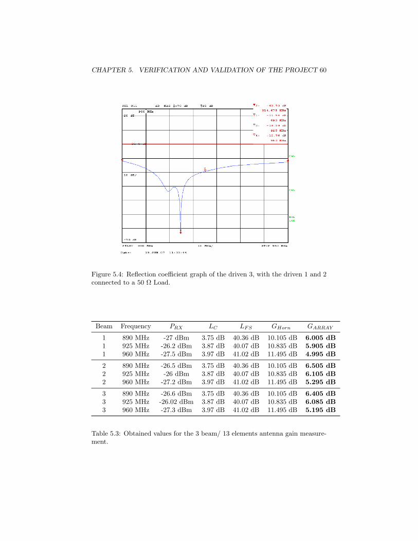
CHAPTER 5. VERIFICATION AND VALIDATION OF THE PROJECT 60
Figure 5.4: Reflection coefficient graph of the driven 3, with the driven 1 and 2connected to a 50 Ω Load.
Beam Frequency PRX LC LFS GHorn GARRAY
1 890 MHz -27 dBm 3.75 dB 40.36 dB 10.105 dB 6.005 dB1 925 MHz -26.2 dBm 3.87 dB 40.07 dB 10.835 dB 5.905 dB1 960 MHz -27.5 dBm 3.97 dB 41.02 dB 11.495 dB 4.995 dB
2 890 MHz -26.5 dBm 3.75 dB 40.36 dB 10.105 dB 6.505 dB2 925 MHz -26 dBm 3.87 dB 40.07 dB 10.835 dB 6.105 dB2 960 MHz -27.2 dBm 3.97 dB 41.02 dB 11.495 dB 5.295 dB
3 890 MHz -26.6 dBm 3.75 dB 40.36 dB 10.105 dB 6.405 dB3 925 MHz -26.02 dBm 3.87 dB 40.07 dB 10.835 dB 6.085 dB3 960 MHz -27.3 dBm 3.97 dB 41.02 dB 11.495 dB 5.195 dB
Table 5.3: Obtained values for the 3 beam/ 13 elements antenna gain measure-ment.

CHAPTER 5. VERIFICATION AND VALIDATION OF THE PROJECT 61
5.2.4 Radiation Pattern Test
This test was achieved in the anechoic chamber. The antenna array was mountedin a mobile arm, this rotator arm has an accuracy of 977 measurements for the360. This antenna was connected to the reflection port, ( RF Transmitter) andthe receiver antenna was a horn antenna for the 1 GHz band. The measurementsof the received signal were acquired by the computer using the software Rotator.The scenario of the test is shown in the Figure 5.5.
Figure 5.5: Anechoic chamber, where were carry out the measurement of theRadiation pattern, .
The Tx signal was configured between 850 MHz and 1GHz, The markers usedto measure the radiation pattern were the start, center and end frequencies ofthe GSM 900 Band (890, 925 and 960 MHz).
The results of the radiation pattern where plotted with the software Matlab.Each graphic includes the radiation pattern in the azimuth plane of the threebeams as is shown in the Figure 5.6, the elevation angle of the measurementswas 0. Also is included the -3 dB level, to identify the beam width of the eachbeam direction.

CHAPTER 5. VERIFICATION AND VALIDATION OF THE PROJECT 62
Figure 5.6: Real radiation pattern of the three beam directions in the azimuthalplane, 0elevation angle, of the antenna array.

CHAPTER 5. VERIFICATION AND VALIDATION OF THE PROJECT 63
A comparison of the real and the simulated radiation pattern are shown inthe Figure 5.7, the results of the real beam width decreased considerably.
Figure 5.8 shows the radiation pattern in the elevation angle. The azimuthangle was set to 0.
The result of the real and simulated radiation pattern in the elevation planewere plotted with Matlab, to compare the radiation patterns (Figure 5.9). Theresult shows the real maximum gain at the 25, this maximum values matchesthe simulation pattern. However the decrease of the beam width of the realpattern is the main problem, due in the angle of 0the real pattern shows adecrease of 3 dB, exactly the difference between the Simulated and Real gain.
5.2.5 Beam-width
The results of the real beam width is very narrow, compared with the simulation,this can be seen in the previous Figure 5.7 and Figure 5.8, for the azimuthaland elevation plane respectively. The Table 5.4 shows the simulated and realvalues.
Frequency Simulated Beam Width Real Beam Width
890 MHz 175 70
925 MHz 140 70
960 MHz 85 55
Table 5.4: Comparison table of the real beam width and simulated beam width.

CHAPTER 5. VERIFICATION AND VALIDATION OF THE PROJECT 64
Figure 5.7: Comparison plot of the real and simulated radiation pattern, az-imuthal plane, 0elevation angle, of the antenna array.

CHAPTER 5. VERIFICATION AND VALIDATION OF THE PROJECT 65
Figure 5.8: Real radiation pattern of the elevation plane of the antenna array.
Figure 5.9: Comparison plot of the real and simulated radiation patterns, ele-vation plane of the antenna array.

CHAPTER 5. VERIFICATION AND VALIDATION OF THE PROJECT 66
5.3 RF System Test
The tests for the RF system where divided into RF module test and the Split-ter/Combiner module test . The following activities are included to validate thedesign and construction.
5.3.1 RF Module
The electronic workshop of Griffith University fabricated this module, as isshown in the Figure 5.10 this module has two RF port; the antenna port andthe Splitter/combinner port.
SPLITTER/COMBINNERPORT
ANTENNAPORT
Figure 5.10: Photo of the RF module.
The measurement made to the RF module are shown in the Table 5. Withthe Vector Network Analyzer were calculated the Reflection Coefficient S11 ,input impedance Zin see from the input port, and the insertion losses betweenthe Antenna port and the Switch Port, with the switch on and the switch off.
5.3.2 RF Detector Test
The RF power detector was measured increasing the RF power level to theantenna port, from -30 to -1 dbm, The RF power detector, MAX 2016 did notresponse for any change in the input power. The RSSI always gave a DC valueof 0.944 V. This result is due the surface mount device was not soldering withthe necessary technology. In fact the electronic workshop mentioned that theywere not sure if the device would work. However another RF module has beensoldered in another workshop.

CHAPTER 5. VERIFICATION AND VALIDATION OF THE PROJECT 67
Input Frequency Switch S11 Zin Insertion Loss
Antenna port 890 MHz ON -22.5 dB 45.7 Ω 4.42 dBAntenna port 925 MHz ON -19.08 dB 45 Ω 5.34 dBAntenna port 960 MHz ON -15.9 dB 44.1Ω 5.9 dBAntenna port 890 MHz OFF -10.5 dB 41.3 Ω 11.96 dBAntenna port 925 MHz OFF -10.17 dB 41.0 Ω 11.65 dBAntenna port 960 MHz OFF -9.8 dB 40.7 Ω 10.9 dBSplitter Port 890 MHz ON -18.4 dB 44.8 Ω 4.3 dBSplitter Port 925 MHz ON -12.7 dB 42.7 Ω 5.4 dBSplitter Port 960 MHz ON -10.84 dB 45.4 Ω 5.88 dBSplitter Port 890 MHz OFF -7.35 dB 38.0 Ω 12 dBSplitter Port 925 MHz OFF -7.1 dB 37.7 Ω 11.54 dBSplitter Port 960 MHz OFF -7.88 dB 38.7 Ω 11.2 dB
Table 5.5: Measurement of the reflection coefficient , and insertion loss of theRF module, with the switch in ON and OFF state.
5.3.3 Splitter/Combiner Module
The same procedure was performance for the module Splitter/Combiner, asis shown in the Figure 5.11, the module is formed by a sum port, and threeisolated ports. In the measurement, two of the ports were conected to the VNA( Reflection and Transmission ports), and the other two were connected to a 50Ω terminal. The results are shown in the Table 5.6, were is displayed the Inputimpedance Zin of each port and the insertion Loss between the measured portand the sum port.
Measurement port Frequency S11 Zin Insertion loss
Port 1 890 MHz -8.66 dB 39.6 Ω 22 dBPort 1 925 MHz -9.14 dB 40.1 Ω 19 dBPort 1 960 MHz -7.8 dB 38.6 Ω 17.7 dBPort 2 890 MHz -9.89 dB 40.8 Ω 7 dBPort 2 925 MHz -9.1 dB 40.1 Ω 6.8 dBPort 2 960 MHz -11.6 dB 42.1 Ω 6.7 dBPort 3 890 MHz -8.5 dB 39.5 Ω 22.15 dBPort 3 925 MHz -9.06 dB 40.1 Ω 19.4 dBPort 3 960 MHz -7.77 dB 38.6 Ω 17.7 dB
Table 5.6: Measurement of the Reflection coefficient and Insertion loss of theSplitter/Combiner module, between the ports 1,2,3 with the Sum port.

CHAPTER 5. VERIFICATION AND VALIDATION OF THE PROJECT 68
SUM PORT
PORT 3
PORT 1
PORT 2
Figure 5.11: Image of the Splitter/Combinner module.
Isolation
To know it the module is working properly, the splitter should offer 25 to 30 dBisolation in its mid-band range. In the measurement of the isolation with thesum port properly terminated, 25 to 30 dB should be read. Then was removedthe termination. If isolation drops to 6 dB, the power splitter is OK; if isolationis still high, there is an open circuit in the power splitter.
Input port Output port Insolation with 50Ωin the Sum port
Insolation without 50Ωin the Sum port
Port 1 Port 2 -13.88 dB 14.9 dBPort 1 Port 3 -13 dB 14.5 dB
Table 5.7: Measurement of the Insolation of the Splitter/Combiner module,between the ports 1-2 and 1-3 with the sum port terminated to 50 Ω.
The data from the Table 5.7 shows that the module presents problems,because the module did not decrease in 6dB of the isolation. Also the moduleincludes a high amount of losses, if can be seen in details the Figure 5.12, showssome defects in the mounting of the splitter/combiner, It is mounted upsidedown, and was not constructed with the appropriated technology. This pointwas very crucial because, the thickness of the tracks and the ground layer, hasa different size from the requirements.

CHAPTER 5. VERIFICATION AND VALIDATION OF THE PROJECT 69
MANUFACTURE MISTAKES
Figure 5.12: Detail photo of the defects in the construction of the Split-ter/Combinner module.
5.3.4 RF System Complete
The total insertion loss of the RF system were obtained, this value was measuredwith the input power connected to the antenna port, and the sum port of thesplitter module connected to the receiver port of the VNA. The RF modulewas connected to the port 2 of the Splitter module, and the ports 1 and 3 wereterminated to 50 Ω. The result are Shown in the Table 5.8.
Frequency Theoretical Insertion Loss Real Insertion Loss
890 MHz 4.02 dB 11.22 dB925 MHz 4.02 dB 13.05 dB960 MHz 4.02 dB 13.88 dB
Table 5.8: Measurement of the Insertion loss of the RF system.
The values are to high compare with the theory, These losses could be forthe impedance mismatch caused for:
• The tracks of the PCB were tined, and this process change the thickness ofthe micro-strip transmission lines, changing the characteristic impedance.
• The splitter combiner chip, was soldered upside down, this technique usedin the workshop was not appropriated to RF devices, because radiates alot amount of RF energy.

CHAPTER 5. VERIFICATION AND VALIDATION OF THE PROJECT 70
5.4 Control System
5.4.1 ADC Module and Comparator Test
A 10 KΩ potentiometer, was used to change the voltage from 0 to 5V, as shownin the Figure 13. The input voltage value of the micro controller was measuredwith a tester.
To measure the comparator test, a LED connected to ground in series witha 580 Ω resistor, was connected to the output of the micro controller. Thisoutput is connected to the operational amplifier connected like inverter, whichare the control signal of the RF switches, as is shown in the Figure 5.13. Withthis method was visually known which switch was active.
Figure 5.13: Schematic of the ADC and comparator test module.
5.4.2 Switching Latency Test
Using a digital oscilloscope, was measured the fall time response of the RFswitch control signal. As the Figure 5.14 shows the response time as 9 ns. Inthe previous chapter was explained that is necessary to follow this sequence,activate the new antenna direction, wait until the switch has been activatedand then turn off the previous active beam. This was achieved programming adelay time between the switch off and switch on of the RF system. ( note thatthe On signal is -5V and the OFF signal is 0 V).
In the Chapter one was explained the duration of the GSM time slot is 575.92us, divided in 156.25 bits, this gives a bit duration of 3.69 us. The time weretwo antennas are connected to the splitter/combinner is 2.5 us. This meansthat possible destructive interference caused by the phase of the input signalswill affect only to one bit. This bit could be easily corrected by algorithms thatthe RF transceiver uses.

CHAPTER 5. VERIFICATION AND VALIDATION OF THE PROJECT 71
Figure 5.14: Response time of the RF switch control signal.
5.5 Complete System Test
This test could not be achieved, because the PCB of the RF module are infabrication in another workshop. This test will be performance in the nextweeks, when the module arrives.

CHAPTER 5. VERIFICATION AND VALIDATION OF THE PROJECT 72
5.6 Conclusions
The requirements made for the antenna design were not completely satisfying,the reflection coefficient gave good results, with a band width that covers theGSM 900 MHz band from 890 MHz to 960 MHz . Also the obtained gain wasover the 6 dBi, however the radiation pattern in the azimuthal plane, 0elevationangle, suffered a decreasing in the beam width from 140to 70, this results areproduced by a decreasing of the radiation pattern in the elevation angle.
The RF system were not completely satisfied, because the high insertionloss, produced by mistakes and lack of technology in the electronic workshopwith the mounting process of the devices. Also the RF power detector did notwork, for the same reason previous explained. Anyhow, the switching systemworks.
The Control module works perfectly, comparing the values and controllingthe RF switches. Also, the variable gain controller fulfills the requirements.

Chapter 6
General Comments
6.1 Conclusion
The work presented in this thesis was the first approach in the design of asmart antenna GSM 900 for marine applications. Representing a big step in theimplementation of cellular networks in marine applications.
The simulation and optimization of the 3 beam /13 elements antenna arraywas made with the software 4NEC2, using Genetic Algorithms, with a costfunction that maximized the Gain in the edge of the beam width(60azimuthalplane) and minimized the Reflection Coefficient, for the frequency band between890 MHz and 925 MHz. The theoretical results improved the gain to 9.6 dBi ,and the beam width of the each sector is 140and a S11 below -8.2 dB.
Otherwise the real parameter were measured in the anechoic chamber. Thereflection coefficient gave good results, less than -11 dB, with a band width thatcovers the GSM 900 MHz band from 890 MHz to 960 MHz . Also the obtainedgain was over the 6 dBi, however the radiation pattern in the azimuthal plane,0elevation angle, suffered a decreasing in the beam width from 140to 70, thisresults are produced by a decreasing of the radiation pattern in the elevationangle.
This real values do not satisfy completely, the requirements made for the 3beam / 13 elements antenna array.
The solution of the RF system fulfills the requirements for the GSM 900 MHzand for the different scenarios that the Smart Antenna will be exposed. Thepower budget of the RF design showed in the chapter 3, describe the functioningof the RF system working in the secure levels. Also the system was design usingmicro strip transmission lines technic to match the characteristic impedance of50 Ω.
Experimentally the RF system were not completely satisfied, because of thehigh insertion loss, produced by manufactured mistakes and lack of technology inthe electronic workshop with the mounting process of the devices. Also the RFpower detector did not work, for the same reason previous explained. Anyhow
73

CHAPTER 6. GENERAL COMMENTS 74
the switching system works. However the PCB is being mounted in anotherworkshop.
The control module is used to compare the RF power received from eachbeam pattern and obtain the strongest signal, then switch the direction of theantenna to the RF Terminal. This process is performed with a micro controllerAVR ATMega 128.
The Control module works perfectly, comparing the values and controllingthe RF switches. Also the variable gain controller fulfills the requirements.
This project is a novel idea in the marine communications area, becausecurrently does not exist any commercial product like this.
6.2 Future Works
This project was the beginning of the development of the smart antennas forcellular networks for marine applications, which implies a great number of im-provement that could be done in this area, in future researches.
• Reduce the size of the antenna using dielectric embedded antenna theory,with this method the size could be decreased up to 80 %.
• Use a down-converter circuit and process the signals in the intermediumband with FPGA. With this method the number of RF elements willdecrease, avoiding loss for insertion and reflection caused by the impedancemismatching.
• Develop a system for 3G technology. This can be achieved using a com-mercial OEM cellular Module. Also, this module can detect the time whenthe transceiver is not transmitting and receiving data, in this moment theRF system can switch between one antenna to another without problems.Also it could be used to detect the transmitting frequency of the antenna,and switch to the required band pass filter, this idea needs a long time ofresearch.
• Develop from this Idea, a smart repeater. This system has an omnidirec-tional antenna for the cellular band connected at the end of the Smartantenna, this omnidirectional antenna is located inside vessels, like touristcatamaran, ferries, etc.

Bibliography
[1] A. Molisch, Wireless Communications. Wiley-IEEE Press, 2005.
[2] D. T. S. Preston, J. Lu, “Systematic approach to the design of directionalantennas using switched parasitic and swithced active element,” in Proc.APMC, pp. 531–534, Dec. 1998.
[3] T. O. Haruo Kawakami, “Electrically steerable passive array radiator (es-par) antennas,”
[4] N. S. Inc., “Nec, ”antenna analisys software version 5.8.9”,” California,2007.
[5] D. Thiel and S. Smith, Switched Parasitic Antennas for Cellular Commu-nications. Artech House, 2001.
[6] IEEE Standard Definitions of Terms for Antennas. No. 0-7381-4343-X,Antenna Standards Committee of the IEEE Antennas and PropagationGroup, USA;, 1983.
[7] G. association.
[8] R. Blake, Electronic Communication Systems. International Thomson,2001.
[9] Mini-circuits, Technical infromation about Directional Couplers, 1999.
[10] M. Shah, “Smart antenna control system for wireless ad hoc mobile com-puting,” 2005.
[11] “Pcb software creator, altium designer v6.”
[12] C. Sayre, Complete Wireless Design. McGraw-Hill, 2001.
[13] “Microwave impedance calculator (mwij 1.0).”
[14] A. CO., PCB Design Training Module, Altium Designer., training mod-ule ed.
[15] R. Grossblatt, “Issues of radio-electronics,” March 1984.
75

BIBLIOGRAPHY 76
[16] “Multisim simulator, electronic workbench.”
[17] Futurlec, “Et avr stamp avr atmega128.”
[18] P. Stang, “C-language function library for atmel avr processors.”
[19] ATMEL, “Avr studio R© 4, integrated development environment (ide).”
[20] “Open source software development tools for the atmel avr.”
[21] C. Lanconelli., “Ponyprog2000, serial device programer software.”

Appendix A
Code NEC
77

CM Design B: 3Beam/13 Elemnts over the circular ground plane with a skirt. CM Model; Optimization base of the paper Paper Junwei LuCM Skirt 1/4 LamdaCM Re!ector Wire 1, 11 segmentsCM Driven 1 Wire 2, 11 segmentsCM Driven 2 Wire 3, 11 segmentsCM Driven 3 Wire 4, 11 segmentsCM Director 1 Wire 5, 11 segmentsCM Director 2 Wire 6, 11 segmentsCM Director 3 Wire 7, 11 segmentsCM CESY r1=0.081 'Radius inner circleSY r2=0.081 'Radius outter circleSY Lmr=0.221662 'Main Re!ector lengthSY Ldriven=0.053579 'Driven Wire lengthSY Ldirec=0.08057 'Director Wire lengthSY Lcr1=0.24 'Corner Re!ector 1 lengthSY Lcr2=0.200031 'Corner Re!ector 2 lengthSY rmr=9.e-3 'Radius main re!ectorSY rdriven=5.e-3 'Radius of the inner elementsSY rdirec=5.e-4 'Radius of the outer elementsSY rcr1=2.e-3 'Radius of corner re!ectorsSY rcr2=2.e-3 'Radius corner re!ector 2SY d=0.SY s=11 'SegmentationGW 1 s .0 .0 d .0 .0 d+Lmr rmrGW 2 s r1*cos(0) r1*sin(0) d r1*cos(0) r1*sin(0) d+Ldriven rdrivenGW 3 s r1*cos(120) r1*sin(120) d r1*cos(120) r1*sin(120) d+Ldriven rdrivenGW 4 s r1*cos(240) r1*sin(240) d r1*cos(240) r1*sin(240) d+Ldriven rdrivenGW 5 s (r1+r2)*cos(0) (r1+r2)*sin(0) d (r1+r2)*cos(0) (r1+r2)*sin(0) d+Ldirec rdirecGW 6 s (r1+r2)*cos(120) (r1+r2)*sin(120) d (r1+r2)*cos(120) (r1+r2)*sin(120) d+Ldirec rdirecGW 7 s (r1+r2)*cos(240) (r1+r2)*sin(240) d (r1+r2)*cos(240) (r1+r2)*sin(240) d+Ldirec rdirecGW 8 s r1*cos(60) r1*sin(60) d r1*cos(60) r1*sin(60) d+Lcr1 rcr1GW 9 s r1*cos(180) r1*sin(180) d r1*cos(180) r1*sin(180) d+Lcr1 rcr1GW 10 s r1*cos(300) r1*sin(300) d r1*cos(300) r1*sin(300) d+Lcr1 rcr1GW 11 s (r1+r2)*cos(60) (r1+r2)*sin(60) d (r1+r2)*cos(60) (r1+r2)*sin(60) d+Lcr2 rcr2GW 12 s (r1+r2)*cos(180) (r1+r2)*sin(180) d (r1+r2)*cos(180) (r1+r2)*sin(180) d+Lcr2 rcr2GW 13 s (r1+r2)*cos(300) (r1+r2)*sin(300) d (r1+r2)*cos(300) (r1+r2)*sin(300) d+Lcr2 rcr2GW 14 2 .0 .0 .0 .0405 .0 .0 .000002GW 15 2 .0405 .0 .0 .081 .0 .0 .000002GW 16 2 .081 .0 .0 .1215 .0 .0 .000002GW 17 2 .1215 .0 .0 .162 .0 .0 .000002GW 18 2 .162 .0 .0 .2025 .0 .0 .000002GW 19 2 .2025 .0 .0 .243 .0 .0 .000002GW 20 2 .0 .0 .0 .039615 .00842 .0 .000002GW 21 2 .039615 .00842 .0 .07923 .016841 .0 .000002GW 22 2 .07923 .016841 .0 .118845 .025261 .0 .000002GW 23 2 .118845 .025261 .0 .15846 .033682 .0 .000002GW 24 2 .15846 .033682 .0 .198075 .042102 .0 .000002GW 25 2 .198075 .042102 .0 .23769 .050523 .0 .000002GW 26 2 .0 .0 .0 .036999 .016473 .0 .000002GW 27 2 .036999 .016473 .0 .073997 .032946 .0 .000002GW 28 2 .073997 .032946 .0 .110996 .049419 .0 .000002GW 29 2 .110996 .049419 .0 .147994 .065891 .0 .000002GW 30 2 .147994 .065891 .0 .184993 .082364 .0 .000002GW 31 2 .184993 .082364 .0 .221992 .098837 .0 .000002GW 32 2 .0 .0 .0 .032765 .023805 .0 .000002GW 33 2 .032765 .023805 .0 .06553 .047611 .0 .000002GW 34 2 .06553 .047611 .0 .098296 .071416 .0 .000002GW 35 2 .098296 .071416 .0 .131061 .095221 .0 .000002GW 36 2 .131061 .095221 .0 .163826 .119027 .0 .000002GW 37 2 .163826 .119027 .0 .196591 .142832 .0 .000002GW 38 2 .0 .0 .0 .0271 .030097 .0 .000002GW 39 2 .0271 .030097 .0 .0542 .060195 .0 .000002GW 40 2 .0542 .060195 .0 .081299 .090292 .0 .000002GW 41 2 .081299 .090292 .0 .108399 .120389 .0 .000002GW 42 2 .108399 .120389 .0 .135499 .150487 .0 .000002GW 43 2 .135499 .150487 .0 .162599 .180584 .0 .000002GW 44 2 .0 .0 .0 .02025 .035074 .0 .000002GW 45 2 .02025 .035074 .0 .0405 .070148 .0 .000002GW 46 2 .0405 .070148 .0 .06075 .105222 .0 .000002GW 47 2 .06075 .105222 .0 .081 .140296 .0 .000002GW 48 2 .081 .140296 .0 .10125 .17537 .0 .000002GW 49 2 .10125 .17537 .0 .1215 .210444 .0 .000002GW 50 2 .0 .0 .0 .012515 .038518 .0 .000002GW 51 2 .012515 .038518 .0 .02503 .077036 .0 .000002GW 52 2 .02503 .077036 .0 .037546 .115553 .0 .000002GW 53 2 .037546 .115553 .0 .050061 .154071 .0 .000002GW 54 2 .050061 .154071 .0 .062576 .192589 .0 .000002GW 55 2 .062576 .192589 .0 .075091 .231107 .0 .000002GW 56 2 .0 .0 .0 .004233 .040278 .0 .000002GW 57 2 .004233 .040278 .0 .008467 .080556 .0 .000002GW 58 2 .008467 .080556 .0 .0127 .120834 .0 .000002GW 59 2 .0127 .120834 .0 .016934 .161113 .0 .000002GW 60 2 .016934 .161113 .0 .021167 .201391 .0 .000002GW 61 2 .021167 .201391 .0 .0254 .241669 .0 .000002GW 62 2 .0 .0 .0 -.004233 .040278 .0 .000002GW 63 2 -.004233 .040278 .0 -.008467 .080556 .0 .000002GW 64 2 -.008467 .080556 .0 -.0127 .120834 .0 .000002GW 65 2 -.0127 .120834 .0 -.016934 .161113 .0 .000002GW 66 2 -.016934 .161113 .0 -.021167 .201391 .0 .000002GW 67 2 -.021167 .201391 .0 -.0254 .241669 .0 .000002GW 68 2 .0 .0 .0 -.012515 .038518 .0 .000002GW 69 2 -.012515 .038518 .0 -.02503 .077036 .0 .000002GW 70 2 -.02503 .077036 .0 -.037546 .115553 .0 .000002GW 71 2 -.037546 .115553 .0 -.050061 .154071 .0 .000002GW 72 2 -.050061 .154071 .0 -.062576 .192589 .0 .000002GW 73 2 -.062576 .192589 .0 -.075091 .231107 .0 .000002GW 74 2 .0 .0 .0 -.02025 .035074 .0 .000002GW 75 2 -.02025 .035074 .0 -.0405 .070148 .0 .000002GW 76 2 -.0405 .070148 .0 -.06075 .105222 .0 .000002GW 77 2 -.06075 .105222 .0 -.081 .140296 .0 .000002GW 78 2 -.081 .140296 .0 -.10125 .17537 .0 .000002GW 79 2 -.10125 .17537 .0 -.1215 .210444 .0 .000002GW 80 2 .0 .0 .0 -.0271 .030097 .0 .000002GW 81 2 -.0271 .030097 .0 -.0542 .060195 .0 .000002GW 82 2 -.0542 .060195 .0 -.081299 .090292 .0 .000002GW 83 2 -.081299 .090292 .0 -.108399 .120389 .0 .000002GW 84 2 -.108399 .120389 .0 -.135499 .150487 .0 .000002GW 85 2 -.135499 .150487 .0 -.162599 .180584 .0 .000002GW 86 2 .0 .0 .0 -.032765 .023805 .0 .000002GW 87 2 -.032765 .023805 .0 -.06553 .047611 .0 .000002GW 88 2 -.06553 .047611 .0 -.098296 .071416 .0 .000002GW 89 2 -.098296 .071416 .0 -.131061 .095221 .0 .000002GW 90 2 -.131061 .095221 .0 -.163826 .119027 .0 .000002GW 91 2 -.163826 .119027 .0 -.196591 .142832 .0 .000002GW 92 2 .0 .0 .0 -.036999 .016473 .0 .000002GW 93 2 -.036999 .016473 .0 -.073997 .032946 .0 .000002GW 94 2 -.073997 .032946 .0 -.110996 .049419 .0 .000002GW 95 2 -.110996 .049419 .0 -.147994 .065891 .0 .000002GW 96 2 -.147994 .065891 .0 -.184993 .082364 .0 .000002GW 97 2 -.184993 .082364 .0 -.221992 .098837 .0 .000002GW 98 2 .0 .0 .0 -.039615 .00842 .0 .000002GW 99 2 -.039615 .00842 .0 -.07923 .016841 .0 .000002GW 100 2 -.07923 .016841 .0 -.118845 .025261 .0 .000002GW 101 2 -.118845 .025261 .0 -.15846 .033682 .0 .000002GW 102 2 -.15846 .033682 .0 -.198075 .042102 .0 .000002GW 103 2 -.198075 .042102 .0 -.23769 .050523 .0 .000002GW 104 2 .0 .0 .0 -.0405 .0 .0 .000002GW 105 2 -.0405 .0 .0 -.081 .0 .0 .000002GW 106 2 -.081 .0 .0 -.1215 .0 .0 .000002GW 107 2 -.1215 .0 .0 -.162 .0 .0 .000002GW 108 2 -.162 .0 .0 -.2025 .0 .0 .000002GW 109 2 -.2025 .0 .0 -.243 .0 .0 .000002GW 110 2 .0 .0 .0 -.039615 -.00842 .0 .000002GW 111 2 -.039615 -.00842 .0 -.07923 -.016841 .0 .000002GW 112 2 -.07923 -.016841 .0 -.118845 -.025261 .0 .000002GW 113 2 -.118845 -.025261 .0 -.15846 -.033682 .0 .000002

GW 114 2 -.15846 -.033682 .0 -.198075 -.042102 .0 .000002GW 115 2 -.198075 -.042102 .0 -.23769 -.050523 .0 .000002GW 116 2 .0 .0 .0 -.036999 -.016473 .0 .000002GW 117 2 -.036999 -.016473 .0 -.073997 -.032946 .0 .000002GW 118 2 -.073997 -.032946 .0 -.110996 -.049419 .0 .000002GW 119 2 -.110996 -.049419 .0 -.147994 -.065891 .0 .000002GW 120 2 -.147994 -.065891 .0 -.184993 -.082364 .0 .000002GW 121 2 -.184993 -.082364 .0 -.221992 -.098837 .0 .000002GW 122 2 .0 .0 .0 -.032765 -.023805 .0 .000002GW 123 2 -.032765 -.023805 .0 -.06553 -.047611 .0 .000002GW 124 2 -.06553 -.047611 .0 -.098296 -.071416 .0 .000002GW 125 2 -.098296 -.071416 .0 -.131061 -.095221 .0 .000002GW 126 2 -.131061 -.095221 .0 -.163826 -.119027 .0 .000002GW 127 2 -.163826 -.119027 .0 -.196591 -.142832 .0 .000002GW 128 2 .0 .0 .0 -.0271 -.030097 .0 .000002GW 129 2 -.0271 -.030097 .0 -.0542 -.060195 .0 .000002GW 130 2 -.0542 -.060195 .0 -.081299 -.090292 .0 .000002GW 131 2 -.081299 -.090292 .0 -.108399 -.120389 .0 .000002GW 132 2 -.108399 -.120389 .0 -.135499 -.150487 .0 .000002GW 133 2 -.135499 -.150487 .0 -.162599 -.180584 .0 .000002GW 134 2 .0 .0 .0 -.02025 -.035074 .0 .000002GW 135 2 -.02025 -.035074 .0 -.0405 -.070148 .0 .000002GW 136 2 -.0405 -.070148 .0 -.06075 -.105222 .0 .000002GW 137 2 -.06075 -.105222 .0 -.081 -.140296 .0 .000002GW 138 2 -.081 -.140296 .0 -.10125 -.17537 .0 .000002GW 139 2 -.10125 -.17537 .0 -.1215 -.210444 .0 .000002GW 140 2 .0 .0 .0 -.012515 -.038518 .0 .000002GW 141 2 -.012515 -.038518 .0 -.02503 -.077036 .0 .000002GW 142 2 -.02503 -.077036 .0 -.037546 -.115553 .0 .000002GW 143 2 -.037546 -.115553 .0 -.050061 -.154071 .0 .000002GW 144 2 -.050061 -.154071 .0 -.062576 -.192589 .0 .000002GW 145 2 -.062576 -.192589 .0 -.075091 -.231107 .0 .000002GW 146 2 .0 .0 .0 -.004233 -.040278 .0 .000002GW 147 2 -.004233 -.040278 .0 -.008467 -.080556 .0 .000002GW 148 2 -.008467 -.080556 .0 -.0127 -.120834 .0 .000002GW 149 2 -.0127 -.120834 .0 -.016934 -.161113 .0 .000002GW 150 2 -.016934 -.161113 .0 -.021167 -.201391 .0 .000002GW 151 2 -.021167 -.201391 .0 -.0254 -.241669 .0 .000002GW 152 2 .0 .0 .0 .004233 -.040278 .0 .000002GW 153 2 .004233 -.040278 .0 .008467 -.080556 .0 .000002GW 154 2 .008467 -.080556 .0 .0127 -.120834 .0 .000002GW 155 2 .0127 -.120834 .0 .016934 -.161113 .0 .000002GW 156 2 .016934 -.161113 .0 .021167 -.201391 .0 .000002GW 157 2 .021167 -.201391 .0 .0254 -.241669 .0 .000002GW 158 2 .0 .0 .0 .012515 -.038518 .0 .000002GW 159 2 .012515 -.038518 .0 .02503 -.077036 .0 .000002GW 160 2 .02503 -.077036 .0 .037546 -.115553 .0 .000002GW 161 2 .037546 -.115553 .0 .050061 -.154071 .0 .000002GW 162 2 .050061 -.154071 .0 .062576 -.192589 .0 .000002GW 163 2 .062576 -.192589 .0 .075091 -.231107 .0 .000002GW 164 2 .0 .0 .0 .02025 -.035074 .0 .000002GW 165 2 .02025 -.035074 .0 .0405 -.070148 .0 .000002GW 166 2 .0405 -.070148 .0 .06075 -.105222 .0 .000002GW 167 2 .06075 -.105222 .0 .081 -.140296 .0 .000002GW 168 2 .081 -.140296 .0 .10125 -.17537 .0 .000002GW 169 2 .10125 -.17537 .0 .1215 -.210444 .0 .000002GW 170 2 .0 .0 .0 .0271 -.030097 .0 .000002GW 171 2 .0271 -.030097 .0 .0542 -.060195 .0 .000002GW 172 2 .0542 -.060195 .0 .081299 -.090292 .0 .000002GW 173 2 .081299 -.090292 .0 .108399 -.120389 .0 .000002GW 174 2 .108399 -.120389 .0 .135499 -.150487 .0 .000002GW 175 2 .135499 -.150487 .0 .162599 -.180584 .0 .000002GW 176 2 .0 .0 .0 .032765 -.023805 .0 .000002GW 177 2 .032765 -.023805 .0 .06553 -.047611 .0 .000002GW 178 2 .06553 -.047611 .0 .098296 -.071416 .0 .000002GW 179 2 .098296 -.071416 .0 .131061 -.095221 .0 .000002GW 180 2 .131061 -.095221 .0 .163826 -.119027 .0 .000002GW 181 2 .163826 -.119027 .0 .196591 -.142832 .0 .000002GW 182 2 .0 .0 .0 .036999 -.016473 .0 .000002GW 183 2 .036999 -.016473 .0 .073997 -.032946 .0 .000002GW 184 2 .073997 -.032946 .0 .110996 -.049419 .0 .000002GW 185 2 .110996 -.049419 .0 .147994 -.065891 .0 .000002GW 186 2 .147994 -.065891 .0 .184993 -.082364 .0 .000002GW 187 2 .184993 -.082364 .0 .221992 -.098837 .0 .000002GW 188 2 .0 .0 .0 .039615 -.00842 .0 .000002GW 189 2 .039615 -.00842 .0 .07923 -.016841 .0 .000002GW 190 2 .07923 -.016841 .0 .118845 -.025261 .0 .000002GW 191 2 .118845 -.025261 .0 .15846 -.033682 .0 .000002GW 192 2 .15846 -.033682 .0 .198075 -.042102 .0 .000002GW 193 2 .198075 -.042102 .0 .23769 -.050523 .0 .000002GW 194 1 .0405 .0 .0 .039615 .00842 .0 .000002GW 195 1 .039615 .00842 .0 .036999 .016473 .0 .000002GW 196 1 .036999 .016473 .0 .032765 .023805 .0 .000002GW 197 1 .032765 .023805 .0 .0271 .030097 .0 .000002GW 198 1 .0271 .030097 .0 .02025 .035074 .0 .000002GW 199 1 .02025 .035074 .0 .012515 .038518 .0 .000002GW 200 1 .012515 .038518 .0 .004233 .040278 .0 .000002GW 201 1 .004233 .040278 .0 -.004233 .040278 .0 .000002GW 202 1 -.004233 .040278 .0 -.012515 .038518 .0 .000002GW 203 1 -.012515 .038518 .0 -.02025 .035074 .0 .000002GW 204 1 -.02025 .035074 .0 -.0271 .030097 .0 .000002GW 205 1 -.0271 .030097 .0 -.032765 .023805 .0 .000002GW 206 1 -.032765 .023805 .0 -.036999 .016473 .0 .000002GW 207 1 -.036999 .016473 .0 -.039615 .00842 .0 .000002GW 208 1 -.039615 .00842 .0 -.0405 .0 .0 .000002GW 209 1 -.0405 .0 .0 -.039615 -.00842 .0 .000002GW 210 1 -.039615 -.00842 .0 -.036999 -.016473 .0 .000002GW 211 1 -.036999 -.016473 .0 -.032765 -.023805 .0 .000002GW 212 1 -.032765 -.023805 .0 -.0271 -.030097 .0 .000002GW 213 1 -.0271 -.030097 .0 -.02025 -.035074 .0 .000002GW 214 1 -.02025 -.035074 .0 -.012515 -.038518 .0 .000002GW 215 1 -.012515 -.038518 .0 -.004233 -.040278 .0 .000002GW 216 1 -.004233 -.040278 .0 .004233 -.040278 .0 .000002GW 217 1 .004233 -.040278 .0 .012515 -.038518 .0 .000002GW 218 1 .012515 -.038518 .0 .02025 -.035074 .0 .000002GW 219 1 .02025 -.035074 .0 .0271 -.030097 .0 .000002GW 220 1 .0271 -.030097 .0 .032765 -.023805 .0 .000002GW 221 1 .032765 -.023805 .0 .036999 -.016473 .0 .000002GW 222 1 .036999 -.016473 .0 .039615 -.00842 .0 .000002GW 223 1 .039615 -.00842 .0 .0405 .0 .0 .000002GW 224 1 .081 .0 .0 .07923 .016841 .0 .000002GW 225 1 .07923 .016841 .0 .073997 .032946 .0 .000002GW 226 1 .073997 .032946 .0 .06553 .047611 .0 .000002GW 227 1 .06553 .047611 .0 .0542 .060195 .0 .000002GW 228 1 .0542 .060195 .0 .0405 .070148 .0 .000002GW 229 1 .0405 .070148 .0 .02503 .077036 .0 .000002GW 230 1 .02503 .077036 .0 .008467 .080556 .0 .000002GW 231 1 .008467 .080556 .0 -.008467 .080556 .0 .000002GW 232 1 -.008467 .080556 .0 -.02503 .077036 .0 .000002GW 233 1 -.02503 .077036 .0 -.0405 .070148 .0 .000002GW 234 1 -.0405 .070148 .0 -.0542 .060195 .0 .000002GW 235 1 -.0542 .060195 .0 -.06553 .047611 .0 .000002GW 236 1 -.06553 .047611 .0 -.073997 .032946 .0 .000002GW 237 1 -.073997 .032946 .0 -.07923 .016841 .0 .000002GW 238 1 -.07923 .016841 .0 -.081 .0 .0 .000002GW 239 1 -.081 .0 .0 -.07923 -.016841 .0 .000002GW 240 1 -.07923 -.016841 .0 -.073997 -.032946 .0 .000002GW 241 1 -.073997 -.032946 .0 -.06553 -.047611 .0 .000002GW 242 1 -.06553 -.047611 .0 -.0542 -.060195 .0 .000002GW 243 1 -.0542 -.060195 .0 -.0405 -.070148 .0 .000002GW 244 1 -.0405 -.070148 .0 -.02503 -.077036 .0 .000002GW 245 1 -.02503 -.077036 .0 -.008467 -.080556 .0 .000002GW 246 1 -.008467 -.080556 .0 .008467 -.080556 .0 .000002GW 247 1 .008467 -.080556 .0 .02503 -.077036 .0 .000002GW 248 1 .02503 -.077036 .0 .0405 -.070148 .0 .000002GW 249 1 .0405 -.070148 .0 .0542 -.060195 .0 .000002GW 250 1 .0542 -.060195 .0 .06553 -.047611 .0 .000002GW 251 1 .06553 -.047611 .0 .073997 -.032946 .0 .000002GW 252 1 .073997 -.032946 .0 .07923 -.016841 .0 .000002

GW 253 1 .07923 -.016841 .0 .081 .0 .0 .000002GW 254 2 .1215 .0 .0 .118845 .025261 .0 .000002GW 255 2 .118845 .025261 .0 .110996 .049419 .0 .000002GW 256 2 .110996 .049419 .0 .098296 .071416 .0 .000002GW 257 2 .098296 .071416 .0 .081299 .090292 .0 .000002GW 258 2 .081299 .090292 .0 .06075 .105222 .0 .000002GW 259 2 .06075 .105222 .0 .037546 .115553 .0 .000002GW 260 2 .037546 .115553 .0 .0127 .120834 .0 .000002GW 261 2 .0127 .120834 .0 -.0127 .120834 .0 .000002GW 262 2 -.0127 .120834 .0 -.037546 .115553 .0 .000002GW 263 2 -.037546 .115553 .0 -.06075 .105222 .0 .000002GW 264 2 -.06075 .105222 .0 -.081299 .090292 .0 .000002GW 265 2 -.081299 .090292 .0 -.098296 .071416 .0 .000002GW 266 2 -.098296 .071416 .0 -.110996 .049419 .0 .000002GW 267 2 -.110996 .049419 .0 -.118845 .025261 .0 .000002GW 268 2 -.118845 .025261 .0 -.1215 .0 .0 .000002GW 269 2 -.1215 .0 .0 -.118845 -.025261 .0 .000002GW 270 2 -.118845 -.025261 .0 -.110996 -.049419 .0 .000002GW 271 2 -.110996 -.049419 .0 -.098296 -.071416 .0 .000002GW 272 2 -.098296 -.071416 .0 -.081299 -.090292 .0 .000002GW 273 2 -.081299 -.090292 .0 -.06075 -.105222 .0 .000002GW 274 2 -.06075 -.105222 .0 -.037546 -.115553 .0 .000002GW 275 2 -.037546 -.115553 .0 -.0127 -.120834 .0 .000002GW 276 2 -.0127 -.120834 .0 .0127 -.120834 .0 .000002GW 277 2 .0127 -.120834 .0 .037546 -.115553 .0 .000002GW 278 2 .037546 -.115553 .0 .06075 -.105222 .0 .000002GW 279 2 .06075 -.105222 .0 .081299 -.090292 .0 .000002GW 280 2 .081299 -.090292 .0 .098296 -.071416 .0 .000002GW 281 2 .098296 -.071416 .0 .110996 -.049419 .0 .000002GW 282 2 .110996 -.049419 .0 .118845 -.025261 .0 .000002GW 283 2 .118845 -.025261 .0 .1215 .0 .0 .000002GW 284 2 .162 .0 .0 .15846 .033682 .0 .000002GW 285 2 .15846 .033682 .0 .147994 .065891 .0 .000002GW 286 2 .147994 .065891 .0 .131061 .095221 .0 .000002GW 287 2 .131061 .095221 .0 .108399 .120389 .0 .000002GW 288 2 .108399 .120389 .0 .081 .140296 .0 .000002GW 289 2 .081 .140296 .0 .050061 .154071 .0 .000002GW 290 2 .050061 .154071 .0 .016934 .161113 .0 .000002GW 291 2 .016934 .161113 .0 -.016934 .161113 .0 .000002GW 292 2 -.016934 .161113 .0 -.050061 .154071 .0 .000002GW 293 2 -.050061 .154071 .0 -.081 .140296 .0 .000002GW 294 2 -.081 .140296 .0 -.108399 .120389 .0 .000002GW 295 2 -.108399 .120389 .0 -.131061 .095221 .0 .000002GW 296 2 -.131061 .095221 .0 -.147994 .065891 .0 .000002GW 297 2 -.147994 .065891 .0 -.15846 .033682 .0 .000002GW 298 2 -.15846 .033682 .0 -.162 .0 .0 .000002GW 299 2 -.162 .0 .0 -.15846 -.033682 .0 .000002GW 300 2 -.15846 -.033682 .0 -.147994 -.065891 .0 .000002GW 301 2 -.147994 -.065891 .0 -.131061 -.095221 .0 .000002GW 302 2 -.131061 -.095221 .0 -.108399 -.120389 .0 .000002GW 303 2 -.108399 -.120389 .0 -.081 -.140296 .0 .000002GW 304 2 -.081 -.140296 .0 -.050061 -.154071 .0 .000002GW 305 2 -.050061 -.154071 .0 -.016934 -.161113 .0 .000002GW 306 2 -.016934 -.161113 .0 .016934 -.161113 .0 .000002GW 307 2 .016934 -.161113 .0 .050061 -.154071 .0 .000002GW 308 2 .050061 -.154071 .0 .081 -.140296 .0 .000002GW 309 2 .081 -.140296 .0 .108399 -.120389 .0 .000002GW 310 2 .108399 -.120389 .0 .131061 -.095221 .0 .000002GW 311 2 .131061 -.095221 .0 .147994 -.065891 .0 .000002GW 312 2 .147994 -.065891 .0 .15846 -.033682 .0 .000002GW 313 2 .15846 -.033682 .0 .162 .0 .0 .000002GW 314 3 .2025 .0 .0 .198075 .042102 .0 .000002GW 315 3 .198075 .042102 .0 .184993 .082364 .0 .000002GW 316 3 .184993 .082364 .0 .163826 .119027 .0 .000002GW 317 3 .163826 .119027 .0 .135499 .150487 .0 .000002GW 318 3 .135499 .150487 .0 .10125 .17537 .0 .000002GW 319 3 .10125 .17537 .0 .062576 .192589 .0 .000002GW 320 3 .062576 .192589 .0 .021167 .201391 .0 .000002GW 321 3 .021167 .201391 .0 -.021167 .201391 .0 .000002GW 322 3 -.021167 .201391 .0 -.062576 .192589 .0 .000002GW 323 3 -.062576 .192589 .0 -.10125 .17537 .0 .000002GW 324 3 -.10125 .17537 .0 -.135499 .150487 .0 .000002GW 325 3 -.135499 .150487 .0 -.163826 .119027 .0 .000002GW 326 3 -.163826 .119027 .0 -.184993 .082364 .0 .000002GW 327 3 -.184993 .082364 .0 -.198075 .042102 .0 .000002GW 328 3 -.198075 .042102 .0 -.2025 .0 .0 .000002GW 329 3 -.2025 .0 .0 -.198075 -.042102 .0 .000002GW 330 3 -.198075 -.042102 .0 -.184993 -.082364 .0 .000002GW 331 3 -.184993 -.082364 .0 -.163826 -.119027 .0 .000002GW 332 3 -.163826 -.119027 .0 -.135499 -.150487 .0 .000002GW 333 3 -.135499 -.150487 .0 -.10125 -.17537 .0 .000002GW 334 3 -.10125 -.17537 .0 -.062576 -.192589 .0 .000002GW 335 3 -.062576 -.192589 .0 -.021167 -.201391 .0 .000002GW 336 3 -.021167 -.201391 .0 .021167 -.201391 .0 .000002GW 337 3 .021167 -.201391 .0 .062576 -.192589 .0 .000002GW 338 3 .062576 -.192589 .0 .10125 -.17537 .0 .000002GW 339 3 .10125 -.17537 .0 .135499 -.150487 .0 .000002GW 340 3 .135499 -.150487 .0 .163826 -.119027 .0 .000002GW 341 3 .163826 -.119027 .0 .184993 -.082364 .0 .000002GW 342 3 .184993 -.082364 .0 .198075 -.042102 .0 .000002GW 343 3 .198075 -.042102 .0 .2025 .0 .0 .000002GW 344 3 .243 .0 .0 .23769 .050523 .0 .000002GW 345 3 .23769 .050523 .0 .221992 .098837 .0 .000002GW 346 3 .221992 .098837 .0 .196591 .142832 .0 .000002GW 347 3 .196591 .142832 .0 .162599 .180584 .0 .000002GW 348 3 .162599 .180584 .0 .1215 .210444 .0 .000002GW 349 3 .1215 .210444 .0 .075091 .231107 .0 .000002GW 350 3 .075091 .231107 .0 .0254 .241669 .0 .000002GW 351 3 .0254 .241669 .0 -.0254 .241669 .0 .000002GW 352 3 -.0254 .241669 .0 -.075091 .231107 .0 .000002GW 353 3 -.075091 .231107 .0 -.1215 .210444 .0 .000002GW 354 3 -.1215 .210444 .0 -.162599 .180584 .0 .000002GW 355 3 -.162599 .180584 .0 -.196591 .142832 .0 .000002GW 356 3 -.196591 .142832 .0 -.221992 .098837 .0 .000002GW 357 3 -.221992 .098837 .0 -.23769 .050523 .0 .000002GW 358 3 -.23769 .050523 .0 -.243 .0 .0 .000002GW 359 3 -.243 .0 .0 -.23769 -.050523 .0 .000002GW 360 3 -.23769 -.050523 .0 -.221992 -.098837 .0 .000002GW 361 3 -.221992 -.098837 .0 -.196591 -.142832 .0 .000002GW 362 3 -.196591 -.142832 .0 -.162599 -.180584 .0 .000002GW 363 3 -.162599 -.180584 .0 -.1215 -.210444 .0 .000002GW 364 3 -.1215 -.210444 .0 -.075091 -.231107 .0 .000002GW 365 3 -.075091 -.231107 .0 -.0254 -.241669 .0 .000002GW 366 3 -.0254 -.241669 .0 .0254 -.241669 .0 .000002GW 367 3 .0254 -.241669 .0 .075091 -.231107 .0 .000002GW 368 3 .075091 -.231107 .0 .1215 -.210444 .0 .000002GW 369 3 .1215 -.210444 .0 .162599 -.180584 .0 .000002GW 370 3 .162599 -.180584 .0 .196591 -.142832 .0 .000002GW 371 3 .196591 -.142832 .0 .221992 -.098837 .0 .000002GW 372 3 .221992 -.098837 .0 .23769 -.050523 .0 .000002GW 373 3 .23769 -.050523 .0 .243 .0 .0 .000002GW 374 2 .243 .0 -.081 .243 .0 -.054 .000002GW 375 2 .243 .0 -.054 .243 .0 -.027 .000002GW 376 2 .243 .0 -.027 .243 .0 .0 .000002GW 377 2 .23769 .050523 -.081 .23769 .050523 -.054 .000002GW 378 2 .23769 .050523 -.054 .23769 .050523 -.027 .000002GW 379 2 .23769 .050523 -.027 .23769 .050523 .0 .000002GW 380 2 .221992 .098837 -.081 .221992 .098837 -.054 .000002GW 381 2 .221992 .098837 -.054 .221992 .098837 -.027 .000002GW 382 2 .221992 .098837 -.027 .221992 .098837 .0 .000002GW 383 2 .196591 .142832 -.081 .196591 .142832 -.054 .000002GW 384 2 .196591 .142832 -.054 .196591 .142832 -.027 .000002GW 385 2 .196591 .142832 -.027 .196591 .142832 .0 .000002GW 386 2 .162599 .180584 -.081 .162599 .180584 -.054 .000002GW 387 2 .162599 .180584 -.054 .162599 .180584 -.027 .000002GW 388 2 .162599 .180584 -.027 .162599 .180584 .0 .000002GW 389 2 .1215 .210444 -.081 .1215 .210444 -.054 .000002GW 390 2 .1215 .210444 -.054 .1215 .210444 -.027 .000002GW 391 2 .1215 .210444 -.027 .1215 .210444 .0 .000002

GW 392 2 .075091 .231107 -.081 .075091 .231107 -.054 .000002GW 393 2 .075091 .231107 -.054 .075091 .231107 -.027 .000002GW 394 2 .075091 .231107 -.027 .075091 .231107 .0 .000002GW 395 2 .0254 .241669 -.081 .0254 .241669 -.054 .000002GW 396 2 .0254 .241669 -.054 .0254 .241669 -.027 .000002GW 397 2 .0254 .241669 -.027 .0254 .241669 .0 .000002GW 398 2 -.0254 .241669 -.081 -.0254 .241669 -.054 .000002GW 399 2 -.0254 .241669 -.054 -.0254 .241669 -.027 .000002GW 400 2 -.0254 .241669 -.027 -.0254 .241669 .0 .000002GW 401 2 -.075091 .231107 -.081 -.075091 .231107 -.054 .000002GW 402 2 -.075091 .231107 -.054 -.075091 .231107 -.027 .000002GW 403 2 -.075091 .231107 -.027 -.075091 .231107 .0 .000002GW 404 2 -.1215 .210444 -.081 -.1215 .210444 -.054 .000002GW 405 2 -.1215 .210444 -.054 -.1215 .210444 -.027 .000002GW 406 2 -.1215 .210444 -.027 -.1215 .210444 .0 .000002GW 407 2 -.162599 .180584 -.081 -.162599 .180584 -.054 .000002GW 408 2 -.162599 .180584 -.054 -.162599 .180584 -.027 .000002GW 409 2 -.162599 .180584 -.027 -.162599 .180584 .0 .000002GW 410 2 -.196591 .142832 -.081 -.196591 .142832 -.054 .000002GW 411 2 -.196591 .142832 -.054 -.196591 .142832 -.027 .000002GW 412 2 -.196591 .142832 -.027 -.196591 .142832 .0 .000002GW 413 2 -.221992 .098837 -.081 -.221992 .098837 -.054 .000002GW 414 2 -.221992 .098837 -.054 -.221992 .098837 -.027 .000002GW 415 2 -.221992 .098837 -.027 -.221992 .098837 .0 .000002GW 416 2 -.23769 .050523 -.081 -.23769 .050523 -.054 .000002GW 417 2 -.23769 .050523 -.054 -.23769 .050523 -.027 .000002GW 418 2 -.23769 .050523 -.027 -.23769 .050523 .0 .000002GW 419 2 -.243 .0 -.081 -.243 .0 -.054 .000002GW 420 2 -.243 .0 -.054 -.243 .0 -.027 .000002GW 421 2 -.243 .0 -.027 -.243 .0 .0 .000002GW 422 2 -.23769 -.050523 -.081 -.23769 -.050523 -.054 .000002GW 423 2 -.23769 -.050523 -.054 -.23769 -.050523 -.027 .000002GW 424 2 -.23769 -.050523 -.027 -.23769 -.050523 .0 .000002GW 425 2 -.221992 -.098837 -.081 -.221992 -.098837 -.054 .000002GW 426 2 -.221992 -.098837 -.054 -.221992 -.098837 -.027 .000002GW 427 2 -.221992 -.098837 -.027 -.221992 -.098837 .0 .000002GW 428 2 -.196591 -.142832 -.081 -.196591 -.142832 -.054 .000002GW 429 2 -.196591 -.142832 -.054 -.196591 -.142832 -.027 .000002GW 430 2 -.196591 -.142832 -.027 -.196591 -.142832 .0 .000002GW 431 2 -.162599 -.180584 -.081 -.162599 -.180584 -.054 .000002GW 432 2 -.162599 -.180584 -.054 -.162599 -.180584 -.027 .000002GW 433 2 -.162599 -.180584 -.027 -.162599 -.180584 .0 .000002GW 434 2 -.1215 -.210444 -.081 -.1215 -.210444 -.054 .000002GW 435 2 -.1215 -.210444 -.054 -.1215 -.210444 -.027 .000002GW 436 2 -.1215 -.210444 -.027 -.1215 -.210444 .0 .000002GW 437 2 -.075091 -.231107 -.081 -.075091 -.231107 -.054 .000002GW 438 2 -.075091 -.231107 -.054 -.075091 -.231107 -.027 .000002GW 439 2 -.075091 -.231107 -.027 -.075091 -.231107 .0 .000002GW 440 2 -.0254 -.241669 -.081 -.0254 -.241669 -.054 .000002GW 441 2 -.0254 -.241669 -.054 -.0254 -.241669 -.027 .000002GW 442 2 -.0254 -.241669 -.027 -.0254 -.241669 .0 .000002GW 443 2 .0254 -.241669 -.081 .0254 -.241669 -.054 .000002GW 444 2 .0254 -.241669 -.054 .0254 -.241669 -.027 .000002GW 445 2 .0254 -.241669 -.027 .0254 -.241669 .0 .000002GW 446 2 .075091 -.231107 -.081 .075091 -.231107 -.054 .000002GW 447 2 .075091 -.231107 -.054 .075091 -.231107 -.027 .000002GW 448 2 .075091 -.231107 -.027 .075091 -.231107 .0 .000002GW 449 2 .1215 -.210444 -.081 .1215 -.210444 -.054 .000002GW 450 2 .1215 -.210444 -.054 .1215 -.210444 -.027 .000002GW 451 2 .1215 -.210444 -.027 .1215 -.210444 .0 .000002GW 452 2 .162599 -.180584 -.081 .162599 -.180584 -.054 .000002GW 453 2 .162599 -.180584 -.054 .162599 -.180584 -.027 .000002GW 454 2 .162599 -.180584 -.027 .162599 -.180584 .0 .000002GW 455 2 .196591 -.142832 -.081 .196591 -.142832 -.054 .000002GW 456 2 .196591 -.142832 -.054 .196591 -.142832 -.027 .000002GW 457 2 .196591 -.142832 -.027 .196591 -.142832 .0 .000002GW 458 2 .221992 -.098837 -.081 .221992 -.098837 -.054 .000002GW 459 2 .221992 -.098837 -.054 .221992 -.098837 -.027 .000002GW 460 2 .221992 -.098837 -.027 .221992 -.098837 .0 .000002GW 461 2 .23769 -.050523 -.081 .23769 -.050523 -.054 .000002GW 462 2 .23769 -.050523 -.054 .23769 -.050523 -.027 .000002GW 463 2 .23769 -.050523 -.027 .23769 -.050523 .0 .000002GW 464 3 .243 .0 -.081 .23769 .050523 -.081 .000002GW 465 3 .23769 .050523 -.081 .221992 .098837 -.081 .000002GW 466 3 .221992 .098837 -.081 .196591 .142832 -.081 .000002GW 467 3 .196591 .142832 -.081 .162599 .180584 -.081 .000002GW 468 3 .162599 .180584 -.081 .1215 .210444 -.081 .000002GW 469 3 .1215 .210444 -.081 .075091 .231107 -.081 .000002GW 470 3 .075091 .231107 -.081 .0254 .241669 -.081 .000002GW 471 3 .0254 .241669 -.081 -.0254 .241669 -.081 .000002GW 472 3 -.0254 .241669 -.081 -.075091 .231107 -.081 .000002GW 473 3 -.075091 .231107 -.081 -.1215 .210444 -.081 .000002GW 474 3 -.1215 .210444 -.081 -.162599 .180584 -.081 .000002GW 475 3 -.162599 .180584 -.081 -.196591 .142832 -.081 .000002GW 476 3 -.196591 .142832 -.081 -.221992 .098837 -.081 .000002GW 477 3 -.221992 .098837 -.081 -.23769 .050523 -.081 .000002GW 478 3 -.23769 .050523 -.081 -.243 .0 -.081 .000002GW 479 3 -.243 .0 -.081 -.23769 -.050523 -.081 .000002GW 480 3 -.23769 -.050523 -.081 -.221992 -.098837 -.081 .000002GW 481 3 -.221992 -.098837 -.081 -.196591 -.142832 -.081 .000002GW 482 3 -.196591 -.142832 -.081 -.162599 -.180584 -.081 .000002GW 483 3 -.162599 -.180584 -.081 -.1215 -.210444 -.081 .000002GW 484 3 -.1215 -.210444 -.081 -.075091 -.231107 -.081 .000002GW 485 3 -.075091 -.231107 -.081 -.0254 -.241669 -.081 .000002GW 486 3 -.0254 -.241669 -.081 .0254 -.241669 -.081 .000002GW 487 3 .0254 -.241669 -.081 .075091 -.231107 -.081 .000002GW 488 3 .075091 -.231107 -.081 .1215 -.210444 -.081 .000002GW 489 3 .1215 -.210444 -.081 .162599 -.180584 -.081 .000002GW 490 3 .162599 -.180584 -.081 .196591 -.142832 -.081 .000002GW 491 3 .196591 -.142832 -.081 .221992 -.098837 -.081 .000002GW 492 3 .221992 -.098837 -.081 .23769 -.050523 -.081 .000002GW 493 3 .23769 -.050523 -.081 .243 .0 -.081 .000002GW 494 3 .243 .0 -.054 .23769 .050523 -.054 .000002GW 495 3 .23769 .050523 -.054 .221992 .098837 -.054 .000002GW 496 3 .221992 .098837 -.054 .196591 .142832 -.054 .000002GW 497 3 .196591 .142832 -.054 .162599 .180584 -.054 .000002GW 498 3 .162599 .180584 -.054 .1215 .210444 -.054 .000002GW 499 3 .1215 .210444 -.054 .075091 .231107 -.054 .000002GW 500 3 .075091 .231107 -.054 .0254 .241669 -.054 .000002GW 501 3 .0254 .241669 -.054 -.0254 .241669 -.054 .000002GW 502 3 -.0254 .241669 -.054 -.075091 .231107 -.054 .000002GW 503 3 -.075091 .231107 -.054 -.1215 .210444 -.054 .000002GW 504 3 -.1215 .210444 -.054 -.162599 .180584 -.054 .000002GW 505 3 -.162599 .180584 -.054 -.196591 .142832 -.054 .000002GW 506 3 -.196591 .142832 -.054 -.221992 .098837 -.054 .000002GW 507 3 -.221992 .098837 -.054 -.23769 .050523 -.054 .000002GW 508 3 -.23769 .050523 -.054 -.243 .0 -.054 .000002GW 509 3 -.243 .0 -.054 -.23769 -.050523 -.054 .000002GW 510 3 -.23769 -.050523 -.054 -.221992 -.098837 -.054 .000002GW 511 3 -.221992 -.098837 -.054 -.196591 -.142832 -.054 .000002GW 512 3 -.196591 -.142832 -.054 -.162599 -.180584 -.054 .000002GW 513 3 -.162599 -.180584 -.054 -.1215 -.210444 -.054 .000002GW 514 3 -.1215 -.210444 -.054 -.075091 -.231107 -.054 .000002GW 515 3 -.075091 -.231107 -.054 -.0254 -.241669 -.054 .000002GW 516 3 -.0254 -.241669 -.054 .0254 -.241669 -.054 .000002GW 517 3 .0254 -.241669 -.054 .075091 -.231107 -.054 .000002GW 518 3 .075091 -.231107 -.054 .1215 -.210444 -.054 .000002GW 519 3 .1215 -.210444 -.054 .162599 -.180584 -.054 .000002GW 520 3 .162599 -.180584 -.054 .196591 -.142832 -.054 .000002GW 521 3 .196591 -.142832 -.054 .221992 -.098837 -.054 .000002GW 522 3 .221992 -.098837 -.054 .23769 -.050523 -.054 .000002GW 523 3 .23769 -.050523 -.054 .243 .0 -.054 .000002GW 524 3 .243 .0 -.027 .23769 .050523 -.027 .000002GW 525 3 .23769 .050523 -.027 .221992 .098837 -.027 .000002GW 526 3 .221992 .098837 -.027 .196591 .142832 -.027 .000002GW 527 3 .196591 .142832 -.027 .162599 .180584 -.027 .000002GW 528 3 .162599 .180584 -.027 .1215 .210444 -.027 .000002GW 529 3 .1215 .210444 -.027 .075091 .231107 -.027 .000002GW 530 3 .075091 .231107 -.027 .0254 .241669 -.027 .000002

GW 531 3 .0254 .241669 -.027 -.0254 .241669 -.027 .000002GW 532 3 -.0254 .241669 -.027 -.075091 .231107 -.027 .000002GW 533 3 -.075091 .231107 -.027 -.1215 .210444 -.027 .000002GW 534 3 -.1215 .210444 -.027 -.162599 .180584 -.027 .000002GW 535 3 -.162599 .180584 -.027 -.196591 .142832 -.027 .000002GW 536 3 -.196591 .142832 -.027 -.221992 .098837 -.027 .000002GW 537 3 -.221992 .098837 -.027 -.23769 .050523 -.027 .000002GW 538 3 -.23769 .050523 -.027 -.243 .0 -.027 .000002GW 539 3 -.243 .0 -.027 -.23769 -.050523 -.027 .000002GW 540 3 -.23769 -.050523 -.027 -.221992 -.098837 -.027 .000002GW 541 3 -.221992 -.098837 -.027 -.196591 -.142832 -.027 .000002GW 542 3 -.196591 -.142832 -.027 -.162599 -.180584 -.027 .000002GW 543 3 -.162599 -.180584 -.027 -.1215 -.210444 -.027 .000002GW 544 3 -.1215 -.210444 -.027 -.075091 -.231107 -.027 .000002GW 545 3 -.075091 -.231107 -.027 -.0254 -.241669 -.027 .000002GW 546 3 -.0254 -.241669 -.027 .0254 -.241669 -.027 .000002GW 547 3 .0254 -.241669 -.027 .075091 -.231107 -.027 .000002GW 548 3 .075091 -.231107 -.027 .1215 -.210444 -.027 .000002GW 549 3 .1215 -.210444 -.027 .162599 -.180584 -.027 .000002GW 550 3 .162599 -.180584 -.027 .196591 -.142832 -.027 .000002GW 551 3 .196591 -.142832 -.027 .221992 -.098837 -.027 .000002GW 552 3 .221992 -.098837 -.027 .23769 -.050523 -.027 .000002GW 553 3 .23769 -.050523 -.027 .243 .0 -.027 .000002GW 554 3 .243 .0 .0 .23769 .050523 .0 .000002GW 555 3 .23769 .050523 .0 .221992 .098837 .0 .000002GW 556 3 .221992 .098837 .0 .196591 .142832 .0 .000002GW 557 3 .196591 .142832 .0 .162599 .180584 .0 .000002GW 558 3 .162599 .180584 .0 .1215 .210444 .0 .000002GW 559 3 .1215 .210444 .0 .075091 .231107 .0 .000002GW 560 3 .075091 .231107 .0 .0254 .241669 .0 .000002GW 561 3 .0254 .241669 .0 -.0254 .241669 .0 .000002GW 562 3 -.0254 .241669 .0 -.075091 .231107 .0 .000002GW 563 3 -.075091 .231107 .0 -.1215 .210444 .0 .000002GW 564 3 -.1215 .210444 .0 -.162599 .180584 .0 .000002GW 565 3 -.162599 .180584 .0 -.196591 .142832 .0 .000002GW 566 3 -.196591 .142832 .0 -.221992 .098837 .0 .000002GW 567 3 -.221992 .098837 .0 -.23769 .050523 .0 .000002GW 568 3 -.23769 .050523 .0 -.243 .0 .0 .000002GW 569 3 -.243 .0 .0 -.23769 -.050523 .0 .000002GW 570 3 -.23769 -.050523 .0 -.221992 -.098837 .0 .000002GW 571 3 -.221992 -.098837 .0 -.196591 -.142832 .0 .000002GW 572 3 -.196591 -.142832 .0 -.162599 -.180584 .0 .000002GW 573 3 -.162599 -.180584 .0 -.1215 -.210444 .0 .000002GW 574 3 -.1215 -.210444 .0 -.075091 -.231107 .0 .000002GW 575 3 -.075091 -.231107 .0 -.0254 -.241669 .0 .000002GW 576 3 -.0254 -.241669 .0 .0254 -.241669 .0 .000002GW 577 3 .0254 -.241669 .0 .075091 -.231107 .0 .000002GW 578 3 .075091 -.231107 .0 .1215 -.210444 .0 .000002GW 579 3 .1215 -.210444 .0 .162599 -.180584 .0 .000002GW 580 3 .162599 -.180584 .0 .196591 -.142832 .0 .000002GW 581 3 .196591 -.142832 .0 .221992 -.098837 .0 .000002GW 582 3 .221992 -.098837 .0 .23769 -.050523 .0 .000002GW 583 3 .23769 -.050523 .0 .243 .0 .0 .000002GE 0LD 4 3 1 0 50
'Load in the Driven 2LD 4 4 1 0 50
'Load in the Driven 3GN -1EKEX 0 2 1 11 1 0 'Voltage source (1+j0) at wire 2 segment 1.EN

Appendix B
Schematic of the RFmodule
83

APPENDIX B. SCHEMATIC OF THE RF MODULE 84

Appendix C
Schematic of theSplitter/Combiner module
85

Appendix D
PCB layout of the ”RF”module
86

Appendix E
PCB layout of theSplitter/Combiner” module
87

Appendix F
Devices Values
Figure F.1: Values of the electronic devices used in the PCB design.
88

Appendix G
Control System Schematic
89

APPENDIX G. CONTROL SYSTEM SCHEMATIC 90
12
34
ABCD
43
21
D C B AT
itle
Num
ber
Rev
isio
nS
ize
A4
Dat
e:5-A
pr-
2006
Shee
t o
f F
ile:
D:\
ET
-BA
SE
AT
meg
a64_128.D
db
Dra
wn B
y:
XT
AL
124
XT
AL
223
VCC21
VCC52
GND22
GND53
PE
N1
PA
0(A
D0)
51
PA
1(A
D1)
50
PA
2(A
D2)
49
PA
3(A
D3)
48
PA
4(A
D4)
47
PA
5(A
D5)
46
PA
6(A
D6)
45
PA
7(A
D7)
44
PB
0(S
S)
10
PB
1(S
CK
)11
PB
2(M
OS
I)12
PB
3(M
ISO
)13
PB
4(O
C0)
14
PB
5(O
C1A
)15
PB
6(O
C1B
)16
PB
7(0
C2/O
C1C
)17
PC
0(A
8)
35
PC
1(A
9)
36
PC
2(A
10)
37
PC
3(A
11)
38
PC
4(A
12)
39
PC
5(A
13)
40
PC
6(A
14)
41
PC
7(A
15)
42
PD
0(S
CL
/IN
T0)
25
PD
1(S
DA
/IN
T1)
26
PD
2(R
XD
1/I
NT
2)
27
PD
3(T
XD
1/I
NT
3)
28
PD
4(I
CP
1)
29
PD
5(X
CK
1)
30
PD
6(T
1)
31
PD
7(T
2)
32
PG
0(W
R)
33
PG
1(R
D)
34
PG
2(A
LE
)43
PG
3(T
OS
C2)
18
PG
4(T
OS
C1)
19
RE
SE
T20
PF
7(A
DC
7/T
DI)
54
PF
6(A
DC
6/T
DO
)55
PF
5(A
DC
5/T
MS
)56
PF
4(A
DC
4/T
CK
)57
PF
3(A
DC
3)
58
PF
2(A
DC
2)
59
PF
1(A
DC
1)
60
PF
0(A
DC
0)
61
GN
D63
AR
EF
62
AV
CC
64
PE
7(I
CP
3/I
NT
7)
9P
E6(T
3/I
NT
6)
8P
E5(O
C3C
/IN
T5)
7P
E4(O
C3B
/IN
T4)
6P
E3(O
C3A
/AIN
1)
5P
E2(X
CK
0/A
IN0)
4P
E1(T
XD
0/P
DO
)3
PE
0(R
XD
0/P
DI)
2
16M
Hz
22pF
22pF
10
10k
RE
SE
T
+5V
RE
SE
T
PA
0
PE
7P
E6
PE
5P
E4
PE
3P
E2
PE
1P
E0
PA
1P
A2
PA
3P
A4
PA
5P
A6
PA
7
PB
0P
B1
PB
2P
B3
PB
4P
B5
PB
6P
B7
PC
0P
C1
PC
2P
C3
PC
4P
C5
PC
6P
C7
PD
0P
D1
PD
2P
D3
PD
4P
D5
PD
6P
D7
PF
7P
F6
PF
5P
F4
PF
3P
F2
PF
1P
F0
PG
0P
G1
PG
2P
G3
PG
410k
+5V
12
34
56
78
910
ISP
LO
AD
12
34
56
78
910
PO
RT
A
PC
1P
C3
PC
5P
C7
PC
0P
C2
PC
4P
C6
GN
D+
5V
0.1
uF
+5V
0.1
uF
+5V
+5V
PE
1
PE
0
GN
D
RE
SE
TP
B1
+5V
GN
DM
ISO
MO
SI
SC
K
MO
SI
MIS
O
SC
K
RE
SE
T
AT
ME
GA
64/1
28
RE
SE
T
12
34
56
78
910
PO
RT
B
PB
1P
B3
PB
5P
B7
PB
0P
B2
PB
4P
B6
GN
D+
5V
12
34
56
78
910
PO
RT
C
PC
1P
C3
PC
5P
C7
PC
0P
C2
PC
4P
C6
GN
D+
5V
12
34
56
78
910
PO
RT
D
PD
1P
D3
PD
5P
D7
PD
0P
D2
PD
4P
D6
GN
D+
5V
12
34
56
78
910
PO
RT
E
PE
1P
E3
PE
5P
E7
PE
0P
E2
PE
4P
E6
GN
D+
5V
12
34
56
78
910
PO
RT
F
PF
1P
F3
PF
5P
F7
PF
0P
F2
PF
4P
F6
GN
D+
5V
10
0.1
uF
12
34
56
78
910
11
12
13
14
ET
-CL
CD
10K
GN
D
+5V
VO
RW
D0
D2
D4
D6
+V
D1
D3
RS
EN
D5
D7
PG
0P
G2
PG
1P
G3
PG
4P
D7
C1+
1
C1-
3
C2+
4
C2-
5
R1O
12
T1I
11
R2O
9
T2I
10
VC
C16
V+
2
V-
6
GN
D15
R1I
13
T1O
14
R2I
8
T2O
7
ICL
3232
1 2 3 4
RS
232-C
H0
1 2 3 4
RS
232-C
H1
+5V
+5V
0.1
uF
+5V
PD
2P
D3
PE
0P
E1
RX
DT
XD
RX
DT
XD
RX
D1
TX
D1
RX
D0
TX
D0
0.1
uF
0.1
uF
0.1
uF
0.1
uF
Adis
ak C
hooch
an
ET
T C
O.,L
TD
. (W
WW
.ET
T.C
O.T
H)
Rev
0
ET
-BA
SE
AV
R A
TM
EG
A64/1
28
Vin
GND
Vout
7805
0.1
uF
0.1
uF
100uF
/25V
10uF
/16V
+5V
7-1
2V
DC
1N
4001
RSSI
1
RSSI
3
RSSI
2
Cont
rol
Switc
h 1.
B
Cont
rol
Switc
h 1.
A
Cont
rol
Switc
h 3.
B
Cont
rol
Switc
h 3.
A
Cont
rol
Switc
h 2.
A
Cont
rol
Switc
h 2.
B
Cont
rol A
mp3
RF1
Cont
rol A
mp3
RF2
Cont
rol A
mp3
RF3

Appendix H
Datasheets RF System
91

APPENDIX H. DATASHEETS RF SYSTEM 92
Dev
ice
Mod
elSu
pply
UR
L
Cou
pler
SCD
C-1
1-2
Min
icir
cuit
shttp://www.minicircuits.com/pdfs/SCDC-11-2.pdf
Am
plifi
er1
MA
X26
40E
UT
+M
axim
http://datasheets.maxim-ic.com/en/ds/MAX2640-MAX2641.pdf
Filt
erT
A94
7FG
Gol
ledg
ehttp://www.golledge.com/pdf/products/saw/gsrf.pdf
Am
plifi
er2
VN
A-2
3M
inic
ircu
its
http://www.minicircuits.com/pdfs/VNA-23.pdf
Gai
nA
mpl
ifier
MA
X20
56E
TX
+M
axim
http://datasheets.maxim-ic.com/en/ds/MAX2056.pdf
RF
Pow
erD
etec
tor
MA
X20
16E
TI+
Max
imhttp://datasheets.maxim-ic.com/en/ds/MAX2016.pdf
Swit
chM
SWA
-2-2
0+M
inic
ircu
its
http://www.minicircuits.com/pdfs/MSWA-2-20.pdf
Split
ter
SCN
-3-1
3+M
inic
ircu
its
http://www.minicircuits.com/pdfs/SCN-3-13.pdf

Appendix I
Datasheets Control System
93

APPENDIX I. DATASHEETS CONTROL SYSTEM 94
Dev
ice
Mod
elU
RL
Mic
roco
ntro
ller
AV
RA
TM
ega
128
http://www.atmel.com/dyn/products/datasheets.aspfamilyid=607
SPI
Pro
gram
erL
M74
05http://www.futurlec.com.au/ET-AVR\_Stamp.jsp
5VV
olta
gere
gula
tor
LM
7805
http://www.ortodoxism.ro/datasheets/fairchild/LM7805.pdf
-9V
Vol
tage
regu
lato
rL
M79
09http://www.datasheets.org.uk/datasheet.php?article=2028216
Tim
er55
5L
M74
05http://www.national.com/pf/LM/LM555.html
Ope
rati
onal
Am
plifi
erL
M74
1http://www.national.com/pf/LM/LM741.html
Tra
nsis
tor
BC
548
http://www.ortodoxism.ro/datasheets/fairchild/BC548.pdf

Appendix J
Code control.c
95

//*****************************************************************************
//
// File Name : 'control.c'
// Title : Control Electronically Switched Multiple Beam Antenna
// Author : Néstor Hernández
// Version : 1.1
//
//*****************************************************************************
#define F_CPU 16000000
#define DELAY_MS 10000
#include <avr/io.h>
#include <avr/interrupt.h>
#include <util/delay.h>
#include "global.h"
#include "a2d.h"
//! Software flag used to indicate when
/// the a2d conversion is complete.
volatile unsigned char a2dCompleteFlag;
//global variables
int num=0;
int short x=0, y=0, z=0, k=0, u=0;
// functions
// initialize a2d converter
void a2dInit(void)
sbi(ADCSR, ADEN); // enable ADC (turn on ADC power)
cbi(ADCSR, ADFR); // default to single sample
convert mode
a2dSetPrescaler(ADC_PRESCALE); // set default prescaler
a2dSetReference(ADC_REFERENCE); // set default reference
cbi(ADMUX, ADLAR); // set to right-adjusted result
sbi(ADCSR, ADIE); // enable ADC interrupts
a2dCompleteFlag = FALSE; // clear conversion complete flag
sei(); // turn on interrupts (if
not already on)
// configure A2D converter clock division (prescaling)
void a2dSetPrescaler(unsigned char prescale)
outb(ADCSR, ((inb(ADCSR) & ~ADC_PRESCALE_MASK) | prescale));
// configure A2D converter voltage reference
void a2dSetReference(unsigned char ref)
outb(ADMUX, ((inb(ADMUX) & ~ADC_REFERENCE_MASK) | (ref<<6)));
// Perform a 10-bit conversion
// starts conversion, waits until conversion is done, and returns result
unsigned short a2dConvert10bit(unsigned char ch)

a2dCompleteFlag = FALSE; // clear conversion
complete flag
outb(ADMUX, (inb(ADMUX) & ~ADC_MUX_MASK) | (ch & ADC_MUX_MASK)); // set
channel
sbi(ADCSR, ADIF); // clear hardware
"conversion complete" flag
sbi(ADCSR, ADSC); // start
conversion
//while(!a2dCompleteFlag); // wait until conversion
complete
//while( bit_is_clear(ADCSR, ADIF) ); // wait until conversion complete
while( bit_is_set(ADCSR, ADSC) ); // wait until conversion complete
// CAUTION: MUST READ ADCL BEFORE ADCH!!!
return (inb(ADCL) | (inb(ADCH)<<8)); // read ADC (full 10 bits);
// *********MAIN*************************************************
int main(void)
a2dInit(); // Init ADC
DDRA=0xFF; //Set pins port A as output
DDRB=0xFF; //Set pins port B as output.
PORTB=0x81;
PORTA=0x29;
newmax=0;
lastmax=1;
while(1)
a2d();
compare();
if (newmax!=lastmax)
switchControl();
lastmax=newmax;
ampControl();
PORTD=0x00;
mydelay(600);
mydelay(600);
return 0;
//*************************************************************
// *********ANALOG DIGITAL CONVERTER**************
//Measure signals strength
void a2d(void)
int i;
// Make conversion and save the values in the array valuea2d
//Pins F.0, F.1 and F.2
for(i=0; i<3;i++)

valuea2d[i]=a2dConvert10bit(i);
//*************************************************************
//********COMPARATION********************************
unsigned short int compare(void)
int i;
max=valuea2d[0];
newmax=0;
//Compare values. Get maximum
for(i=1;i<3;i++)
if(valuea2d[i]>max)
max=valuea2d[i];
newmax=i;
/*
if(valuea2d[1]>max)
max=valuea2d[1];
newmax=1;
else
if(valuea2d[2]>max)
max=valuea2d[2];
newmax=2;
else
newmax=0;
*/
return newmax;
//*************************************************************
//********SWITCH CONTROL********************************
void switchControl(void)
//Set the proper switch On
switch(newmax)
case 0:

if(lastmax=1)
PORTA=0x25;
usdelay();
PORTA=0x29;
if(lastmax=2)
PORTA=0x19;
usdelay();
PORTA=0x29;
break;
case 1:
if(lastmax=0)
PORTA=0x25;
usdelay();
PORTA=0x26;
if(lastmax=2)
PORTA=0x16;
usdelay();
PORTA=0x26;
break;
case 2:
if(lastmax=0)
PORTA=0x19;
usdelay();
PORTA=0x1A;
if(lastmax=1)
PORTA=0x16;
usdelay();
PORTA=0x1A;
break;
//******************************************************************
//*********AMP CONTROL*********************************
//
void ampControl(void)
if(max>479)
PORTB=0x81; //AMP Off
else
if(max<268)

PORTB=0x00; // AMP On
//**************************************************************
void mydelay(int num)
for(x=0;x<num;x++) // THIS IS the timing loop, very critical
for(y=0;y<255;y++)
for(z=0;z<10;z++)
k++; //do something to satisfy avr-gcc
num=0;
k=0;
//**************************************************************
void usdelay(void)
u=0;
for(u=0;u<9;u++) // THIS IS the timing loop, very critical
;

Appendix K
Cost of the project
101

APPENDIX K. COST OF THE PROJECT 102
#D
EVIC
EM
OD
EL
Supplie
rU
NIT
SPa
ckPR
ICE (
UN
IT)
PRIC
E1
Couple
rSCD
C-1
1-2
Min
icircu
its
44
$11.9
5$47.8
02
Am
plif
ier1
MAX2640EU
T+
Max
im4
4$1.2
5$5.0
02.1
C1 4
70 p
F8819688 (
0402)
Farn
ell
44
$0.0
5$0.2
02.2
C2 3
pF
SM
D3.3
/2 (
0603)
Min
ikits
44
$1.7
0$6.8
02.3
C3 4
70 p
F8819688 (
0402)
Farn
ell
44
$0.0
5$0.2
02.3
Z1 9
.85 n
H1198376 (
0603)
Farn
ell
44
$0.5
3$2.1
22.4
ZM
1 2
pF
SM
D2.2
/2 (
0603)
Min
ikits
44
$1.7
0$6.8
03
Filter
TA947FG
Golle
dge
36
$9.5
7$57.4
24
Am
plif
ier2
VN
A-2
3M
inic
ircu
its
44
$3.8
0$15.2
04.1
C3 4
70 p
F8819688 (
0402)
Farn
ell
44
$0.0
5$0.2
05
Gai
n A
mplif
ier
MAX2056ETX+
Max
im4
4$10.7
7$43.0
85.1
C1 4
7pF
8819670 (
0402)
Farn
ell
16
16
$0.0
2$0.3
25.2
C2 1
000 p
F8819556 (
0402)
Farn
ell
16
16
$0.0
7$1.1
25.3
C3 3
.9 p
F1100625 (
0402)
Farn
ell
44
$1.2
4$4.9
65.4
C4 0
,1 u
F7569556 (
0603)
Farn
ell
12
12
$0.1
8$2.1
65.5
R1 1
.2 K
ohm
9239243 (
0402)
Farn
ell
44
$0.1
6$0.6
45.6
R2 3
.95 K
ohm
9239308 (
0402)
Farn
ell
44
$0.1
6$0.6
46
RF
Pow
er D
etec
tor
MAX2016ETI+
Max
im3
3$14.8
3$44.4
96.1
C4 6
80 p
F uc
3019378 (
0402)
Farn
ell
12
12
$0.2
0$2.4
06.2
C5 3
3 p
F uc
8819645 (
0402)
Farn
ell
12
12
$0.0
2$0.2
46.3
C6 0
.1 u
F 7569556 (
0603)
Farn
ell
12
12
$0.1
8$2.1
66.4
C7 1
0uF
(Cca
se)
Tanta
lium
9753907 (
C c
ase)
Farn
ell
33
$0.4
5$1.3
56.5
R0 3
7.4
Ohm
(1206)
4221709 (
0603)
Farn
ell
350
$0.0
4$2.0
07
Sw
ith (
3)
MSW
A-2
-20+
Min
icircu
its
410
$2.4
5$24.5
07.1
R 5
0 o
hm
(0
402)
(47 o
hm
)3898519
Farn
ell
350
$0.0
9$4.5
08
Split
ter
(1)
SCN
-3-1
3+
Min
icircu
its
11
$7.9
5$7.9
58.1
R1 1
24 O
hm
(2)
1170695 (
0603)
Farn
ell
250
$0.0
4$2.0
08.2
R 1
27ohm
(1206)
420177
Farn
ell
150
$0.1
1$5.5
09
Sta
mp A
VR A
TM
ega1
28
Sta
mp A
TM
ega1
28
Futu
rlec
11
$29.1
3$29.1
39.1
ATM
EG
A S
PI P
rogra
mer
ATM
EG
A8535L-
8PI
Futu
rlec
11
$5.4
0$5.4
010.1
FR4 D
ouble
d s
ide
Boar
dFR
4Sute
ck1
1$30.0
0$30.0
010.1
Rods
Hobbyo
ne
11
$24.0
0$24.0
0TO
TAL
$326.28
RF
CO
NTRO
L
AN
TEN
NA

Appendix L
Planning Report
103

4001ENG INDUSTRIAL AFFILIATES PROGRAM
PLANNING REPORT
“SMART ANTENNA GSM 900 MHz FOR MARINE APPLICATIONS”
NESTOR HERNANDEZ
13/4/2007

PLANNING REPORT NESTOR HERNANDEZ S2612872
ESMB FOR GSM 800/2000 MHz IN MARINE APPLICATIONS
2
CONTENTS
1. Introduction Page 3
1.1 Project description Page 3
1.2 Project Stakeholders Page 4
1.2.1 Student detail Page 4
1.2.2 Industry partner Page 4
1.2.3 Project supervisor Page 4
2. Technical specifications Page 5
2.1 Antenna system Page 5
2.2 RF system Page 6
2.3 Control system Page 7
2.4 Benefits and costs Page 8
2.4.1 Benefits Page 8
2.4.2 Costs Page 8
3. Program schedule Page 9
3.1 Scoping diagram Page 9
3.2 Resources estimates Page 9
3.3 Gantt chart Page 10
3.4 Project outcomes Page 11
4. Risk assessment Page 11
5. Quality schedule Page 12
6. Wider professional issues Page 12
7. References Page 13

PLANNING REPORT NESTOR HERNANDEZ S2612872
ESMB FOR GSM 800/2000 MHz IN MARINE APPLICATIONS
3
1. INTRODUCTION
1.1 Project description
GSM communications are continuously increasing their coverage, performance and accessibility,
with this characteristic result so interesting use this technology for other application, like the
communications between the ships and the coast. This project addresses the need to create a multi
directional antenna for the GSM band for marine application. This report explains the method of the
construction of an electronically switched multiple beam antenna. As the boat orientation changes, the
direction of the antenna beam has to change to maintain the communication between the ship and the base
station in the coast. This antenna will have three active elements (monopoles), which cover the azimuthal
plane in 360°. The system automatically detects signal strength from the three directions, selects the
strongest signal and switches, from one beam to another as the ship changes the position and orientation.
The figure 1 shows the block diagram of the project.
Figure 1. Main diagram of the project.
This project is conducted by the industrial partner, associated Professor Junwei Lu, who requires
the construction of this prototype antenna with a gain of 6 [dBi], for the frequencies between 800 [MHz]
and 2000 [MHz] using an hybrid switched-beam Array, with 13 elements based in work previously
published [1].

PLANNING REPORT NESTOR HERNANDEZ S2612872
ESMB FOR GSM 800/2000 MHz IN MARINE APPLICATIONS
4
The main modules of this project are.
• Antenna system: The module consists of an ESMB antenna for the GSM 900 band with 3 possible
beams. The antenna will transmit only for the beam ( zone) with a better position to link the base
station. The antenna will be receiving for the 3 zones.
• RF receiver: Includes the electronic prototype to measure the signal’s strength of each active
element by RF power detectors.
• Control system: Acquire and compares the values of the RF detector output, selects the maximum
value, and active this antenna’s beam to keep the link with the baes station in the coast.
• Antenna direction controller switches the RF source to the monopole which is in a better condition
to transmit, and switches the other two monopoles to an open circuit
1.2 Project stakeholders
This work will be done in the Griffith University, School of Engineering on the Nathan Campus.
1.2.1 Student detail
Student name: Nestor Hernandez
Student Number: s2612872
E-mail: [email protected]
Phone number: 04-20756717
1.2.2 Industry partner
Company name: Centre of Wireless Monitoring and Applications, Griffith University
Company contact: Dr. Junwei Lu
E-mail: [email protected]
Phone number: 373 55118
1.2.3 Projet supervisor.
Name: Dr. Junwei Lu
E-mail: [email protected]
Phone number: 373 55118

PLANNING REPORT NESTOR HERNANDEZ S2612872
ESMB FOR GSM 800/2000 MHz IN MARINE APPLICATIONS
5
2 TECHNICAL SPECIFICATIONS
The system is divided in three main areas, which are follow describe.
2.1 Antenna System
The first part of the project requires the design, simulation and testing of the antenna array with
the follow characteristic.
SPECIFICATONS
s
Operation frequency Between 800 MHz and 2000 MHz Beam position 3 Beam Width ( -3dB ) > 120° Azimuthal plane Gain 6 dBi (directional) Polarization Vertical External connector SMA connector 50 Ω
Table 1. Specifications of the Antenna prototype.
The first design is shown in the figure 2. The array has 13 elements, which consists of a central
reflector element surrounded by 6 arms of 2 elements, 3 arms are configured like reflectors and the other
3 arms are configured like Yagi-Uda antenna with the active elements (S1, S2 and S3) as driver and
follow by one director (D), each active arm is inserted between two reflector arm.
Figure 2. 13 elements array antenna, S1, S2 and S3 are the active elements where is meassure the RF level and
switched the RF voltage.
This array creates a multi-beam antenna with 3 possible beam positions1, 2 and 3 as shown by
the figure 3, providing 360° azimuthal coverage. The structure has been simulated in a previews work [1]
and the optimum length of the elements was found to be: for central reflector R, 0.8λ long with 0.025λ

PLANNING REPORT NESTOR HERNANDEZ S2612872
ESMB FOR GSM 800/2000 MHz IN MARINE APPLICATIONS
6
radius, the other elements were 0.495λ long with a radius of 0.0025λ, and the radial inter-element was
fixed at 0.25λ.
Figure 3. Estimated H plane radiation pattern of the multiple beam antenna. For the three switch positions.
The design and simulations of the antenna models will be made with the software NEC [2] optimizing its performance including extra elements like directors and different kind of reflectors.
2.2 RF system.
The RF system will be continuously measuring the signals strength of the GSM band, coming
from each zone of the antenna. The measure will be make by RF detector devices. Also the system must
include a directional coupler for each detector (see Figure 4). The coupler must communicate the RF
switch and the antenna in both directions, the antenna and the RF detector only in one direction, and do
not communicate the RF detector and the RF switch.
Figure 4. Diagram of the coupler use in the RF system.

PLANNING REPORT NESTOR HERNANDEZ S2612872
ESMB FOR GSM 800/2000 MHz IN MARINE APPLICATIONS
7
2.3 Control system.
A microcontroller will be used to acquire the output values of the RF detectors, determine the
strongest signal, and activate the switches. The microcontroller must have the following features:
• 3 Analog to digital converter (ADC- 8bits),
• 3 digital output ports to control the switch setting.
Figure 5 shows the schematic of the decision system of the strongest signal and the switching
method. The microcontroller measures periodically the output of the RF detectors (V1,V2 and V3),
afterwards compares the three values and identifies the maximum power, then a dc electronic signal
control the switch [3]. When the switch is closed, the monopole is connected with the RF voltage, and
when the switch is opened the monopole is connected to a 50 Ω charge.
Figure 5. Schematic of the control system (the antennas position are not like the figure. Real position, see figure 2) .
The switching can be achieved electronically using active semiconductor devices, p-i-n diodes or
field effect transistor switches, like the Infineon BAR series or by radio frequency
microelectromechanical systems (RF MEMS) switches [5].

PLANNING REPORT NESTOR HERNANDEZ S2612872
ESMB FOR GSM 800/2000 MHz IN MARINE APPLICATIONS
8
2.4 Benefit and Cost
2.4.1 Benefits
The electronically switched multiple-beam antenna has a better performance compare with the
other steering beam antennas, because of their fast response. Also the ESMB antenna have a better power
efficiency compared with the actual antennas used in marine applications, generally omni-directional
antennas. This aspect reduces the cost of the communication system (lower amplifier costs) and decrease
the power supply to the antenna, therefore the electromagnetic pollution is reduced, improving the signal
noise ratio.
The smart antenna system could be sold, with the purpose of reduce cost in amplifiers and
increase the signal quality of the link with the radio-based system through more focused transmission of
radio signals.
2.4.2 Costs The figure 6 shows the list of the cost that will be incurred. This list includes the labour cost of
37.5 hours per weeks of student’s work and 1 hr per week of the academic supervisor’s work. The
prices of the elements are only a first approximation, due is still not defined the correct choice of the
electronic devices.
ITEM #
UNIT COST
A$
TOTAL COST
PER ITEM A$
1 Antenna system
1.1 Prototype Antenna 1 200 200
2 RF system
2.1 RF MENS 3 10 30
2.2 RF Detectors 3 10 30
2.3 Couples 3 36 108
3 Control system
3.1 Kit microcontroller 1 50 50
3.2 Extra elements 10
3.3 Power supply 5V 1 40 40
4 Integration
4.1 PCB for the final assemble 200
5 Final Report
5.1 Reports and documentation 50
TOTAL 1 718
6 Labour cost
6.1 Student 563 20 11,250
6.2 Academic Staff 15 200 3,000
TOTAL 2 14,968 Table 2. Estimation costs of the project.

PLANNING REPORT NESTOR HERNANDEZ S2612872
ESMB FOR GSM 800/2000 MHz IN MARINE APPLICATIONS
9
3 PROGRAM SCHEDULLE
3.1 Scoping diagram.
The following figure 6 shows the list of tasks that are necessaries for the success of this project.
Figure 6. Diagram of project’s tasks.
3.2 Resources estimate
This project requires access to some tools for antenna design and testing. These are:
a. Computer and Internet access: needed for the research activities and simulation.
b. Electromagnetic simulation software: one of the software: NEC [2] or FEMLAB [5] will be
used during the first part of the project designing and simulating the antenna array, the
radiation diagram, the gain, reflection coefficient, etc.
c. Mathematical software: Matlab [6] will be used to plot the real diagram radiation pattern.
d. Anechoic Chamber: in this chamber it will be performed the measurement of the radiation
pattern.
e. Network analyzer: it is necessary to measure the reflection coefficient and the real Bandwidth of the antenna.

PLANNING REPORT NESTOR HERNANDEZ S2612872
ESMB FOR GSM 800/2000 MHz IN MARINE APPLICATIONS
10
f. Protoboard: necessary for assemble of the electronic devices.
g. Digital Oscilloscope: it will measure the output of the RF system.
h. Microcontroller developer kit: need it to program the microcontroller and make some test.
i. PCB design software: it will be used to design the path of the final prototype. 3.3 Gantt Chart
This project has some important activities during the semester, In the figure 6, are shown the most
important tasks, wich are the same that are shown in the figure 7.
Figure 7. Chart Gantt of the project.

PLANNING REPORT NESTOR HERNANDEZ S2612872
ESMB FOR GSM 800/2000 MHz IN MARINE APPLICATIONS
11
3.4 Project outcomes.
The following table 3 shows the relevant deliverables to the Industrial partner and the IAP office.
DATE DELIVERABLES RECIPIENT 12 March Planning Report 23 March Milestone 1 Project confirmation 29 March Milestone 2 Antenna system 18 April Milestone 3 RF detector an Switching system 10 May Milestone 4 Control system 28 May Milestone 5 Complete system 2 April 8 June
Seminar presentation Project thesis and poster
Professor Jun Wei Lu &
Griffith University
29 March Antenna Prototype 18 April RF circuit design and switching system design 10 May Control system design 1 June Full system test
Professor Jun Wei Lu
Table 3. Documents and elements, witch must be delivered.
4 RISKS AND SOLUTIONS
This project contains some risk elements that must be considered, the following list describe them
and identify the strategy to manage those risks.
a. Possible late arrival of necessary components.
Solution: purchase it with anticipations, or have another dealer.
b. Possible damage of the microcontroller.
Solution: this should not happened if it is made a rigorous design of the electronic system, if
some thing wrong happen, the solution is to buy another one and find what was the mistake.
c. Deliver of the antenna prototype with defective.
Solution: send it to fix, and while start the next task on the Gantt chart.
d. Risk if the antenna fails.
Solution: Before construct the antenna prototype, it will be simulated by NEC [2], this
simulation includes radiation pattern and the reflection coefficient S11. The project supervisor
will verify all these results. Anyway, if antenna fails, it will be proceeded to analyze the model,
find the problem, re simulated, contrast the results and send it to manufacture. The ultimate
alternative will be buy 3 directional antennas, and mounted in a base reaching the required
radiation patter.

PLANNING REPORT NESTOR HERNANDEZ S2612872
ESMB FOR GSM 800/2000 MHz IN MARINE APPLICATIONS
12
5 QUALITY SCHEDULE
The table 4 shows the Verification and Validation Plan. The tests will be verified by the project
supervisor, Professor Junwei Lu.
AREA TEST NOTES
Bandwidth measure Using the VNA, it will be measured the reflection coefficient S11 to obtain the bandwidth of the antenna.
Gain measure For this measure it will be used the three antennas technique.
Antenna Test.
Radiation pattern
Anechoic chamber will be used to obtain the data for create the real radiation pattern with matlab [6]
RF detector Test In the RF laboratory, with the oscilloscope will be measured the RF detector’s output under a RF tone transmitted to the antenna. RF system
Test. Impedance Test
The impedance in the RF system will be measure in the cases that the switch will change the position.
Test the ADC module With a potentiometer changing the voltage from 0 to 5V will be test the ADC module.
Test the comparator module
A LED will be connected to each beam control output to test the comparator and know which antenna is active.
Control
systemTest.
Switching latency test The time of the activation of the switch will be
measured. Laboratory test Indoor test of the full system.
Full system test Field test
Outdoor test of the full system measuring the SNR in a real link.
Table 4. Test and verification plan for the project.
6 WIDER PROFESSIONAL ISSUES.
The student will manage this project. He is the responsible for the success of the tasks that are been included in the project schedule. All the activities must be synchronized with the Gantt chart shown in this report. The costs of the devices must be carefully considering at the moment to purchase the elements, in other way; the project will not be profitable. To avoid problems with the schedule, the activities that require the presence of the industrial supervisor must be informed to him with 1 week of anticipation. This project gives important advances to the marine communication systems, bue the energy supplied to the antenna will be smaller than the actual system, ESMB antenna uses the third part of the power required by the omni-directional antennas system used in the ships. This involves the reduction of the cost of the amplifiers, an essential part of the wireless communication system. With this advance will be cheaper obtain a communication system for marine applications.

PLANNING REPORT NESTOR HERNANDEZ S2612872
ESMB FOR GSM 800/2000 MHz IN MARINE APPLICATIONS
13
7 REFERENCES
[1] S. Preston, J. Lu, and D. Thiel, “Systematic approach to the design of directional antennas using
swithced parasitic and swithced active element”, in Proc. APMC, Dec. 1998, pp 531-534.
[2] NEC WIN Professional TM, “ Antenna analisys software version 1.1”. Nittany Scientific Inc.
California, 1997.
[3] D. Thiel, S. Smith, “Switched parasitic antennas for cellular communications”. 2002 Artech House
Inc. ISBN 1-58053-154-7, pag 52.
[4] J. Wei Lu, D. Thiel, “FDTD analisys of Dielectric-Embedded Electronically Switched Multiple-
Beam (DE-ESMB) Antenna Array” pag. 1.
[5] Femlab V.3.2, Comsol.
[6] Matlab V. r2006b, Mathworks.

Appendix M
Milestone Reports
117