submolecular imaging with single particle atomic force
TRANSCRIPT

Mem
ber
of th
e H
elm
holtz
Ass
ocia
tion Submolecular imaging with single particle atomic force sensors
Georgy Kichin
Schlüsseltechnologien / Key TechnologiesBand/ Volume 87ISBN 978-3-89336-976-8 87
Schl
üsse
ltec
hnol
ogie
nK
ey T
echn
olog
ies
Subm
olec
ular
imag
ing
with
ato
mic
forc
e se
nsor
G
eorg
y Ki
chin

Schriften des Forschungszentrums JülichReihe Schlüsseltechnologien / Key Technologies Band / Volume 87


Forschungszentrum Jülich GmbHPeter Grünberg Institut (PGI)Functional Nanostructures at Surfaces (PGI-3)
Submolecular imaging with single particle atomic force sensors
Georgy Kichin
Schriften des Forschungszentrums JülichReihe Schlüsseltechnologien / Key Technologies Band / Volume 87
ISSN 1866-1807 ISBN 978-3-89336-976-8

Bibliographic information published by the Deutsche Nationalbibliothek.The Deutsche Nationalbibliothek lists this publication in the Deutsche Nationalbibliografie; detailed bibliographic data are available in the Internet at http://dnb.d-nb.de.
Publisher and Forschungszentrum Jülich GmbHDistributor: Zentralbibliothek 52425 Jülich Tel: +49 2461 61-5368 Fax: +49 2461 61-6103 Email: [email protected] www.fz-juelich.de/zb Cover Design: Grafische Medien, Forschungszentrum Jülich GmbH
Printer: Grafische Medien, Forschungszentrum Jülich GmbH
Copyright: Forschungszentrum Jülich 2014
Schriften des Forschungszentrums JülichReihe Schlüsseltechnologien / Key Technologies, Band / Volume 87
D 82 (Diss. RWTH Aachen University, 2014)
ISSN 1866-1807ISBN 978-3-89336-976-8
The complete volume is freely available on the Internet on the Jülicher Open Access Server (JUWEL) at www.fz-juelich.de/zb/juwel
Neither this book nor any part of it may be reproduced or transmitted in any form or by any means, electronic or mechanical, including photocopying, microfilming, and recording, or by any information storage and retrieval system, without permission in writing from the publisher.

Abstract
Scanning probe methods with decorated tips is a new trend in surfacestudy. An application of complex probe like a tip with an attached singlemolecule or single atom allows to get new details about the surface proper-ties. It has been shown that the scanning tunnelling hydrogen microscopy(STHM) approach can reach atomic scale resolution and reveals intermolecu-lar interactions. Because of the complexity, this new rapidly developing areais not yet fully understood.
In this work systematic studies of tips decorated with Xe, H2, D2, CO,CH4 was carried out. The tip with a single atom or a single molecule creates asingle particle sensor that simultaneously performs the function of an atomic-scale force sensor and a signal transducer, which couples the short-rangeforce acting on the tip to the tunnelling conductance of the junction. Insome cases the sensor-transducer function of the decorated STM tips canbe quantitatively calibrated. Differences in the performance of the studiedsensors suggest that the sensor functionality can be modified by tuning theinteraction between the sensor particle and the STM tip. Based on force-field calculations, theoretical analysis of the single particle sensor shows aninterrelation between the relative movement of the particle on the tip andcontrast structure of the surface images.
3

4

Kurzfassung
Der Einsatz von Rastersondenmethoden mit funktionalisierten Spitzen istein neuer Trend in der Oberflachen Physik. Eine Anwendung der komplexenSonde aus einer Spitze mit einem einzelnen adsorbierten Molekul oder Atomerlaubt es, neue Details uber die Oberflacheneigenschaften zu erhalten. Eswurde gezeigt, dass mit dem Rastertunnelwasserstoffmikroskopie (STHM)Ansatz eine Auflosung auf atomarer Skala erzielt werden und intermoleku-laren Wechselwirkungen sichtbar gemacht werden konnen. Auf Grund derhohen Komplexitat ist dieses neue, sich rasch entwickelnde Gebiet noch nichtvollstandig verstanden.
In dieser Arbeit wurden systematische Untersuchungen von mit Xe, H2,D2, CO und CH4 besetzten Spitzen durchgefuhrt. Die Spitze mit einemeinzelnen Atom oder Molekul stellt einen Einteilchen-Sensor dar, der gleich-zeitig als atomarer Kraftsensor und Signalwandler fungiert und so die kurz-reichweitigen Krafte, die an der Spitze wirken, mit der Tunnelleitfahigkeit desKontaktes koppelt. In einigen Fallen kann die Sensor-Signalwandlerfunktionder dekorierten STM-Spitzen fur eine quantitative Kalibration genutzt wer-den. Die Unterschiede im Verhalten der untersuchten Sensoren zeigen, dassdie Sensorfunktionalitat durch die Wechselwirkung zwischen Sensorteilchenund STM-Spitze modifiziert werden kann. Auf der Grundlage von Kraftfeld-berechnungen zeigt eine theoretische Analyse der einzelnen Sensorteilcheneine Wechselbeziehung zwischen der relativen Bewegung des Teilchens aufder Spitze und Kontraststruktur der Oberflachenbilder.
5

6

Contents
List of Acronyms 9
Introduction 11
1 Theory of measurements 151.1 STM . . . . . . . . . . . . . . . . . . . . . . . . . . . . . . . . 15
1.1.1 Bardeen approach . . . . . . . . . . . . . . . . . . . . . 171.1.2 Tersoff-Hamann theory . . . . . . . . . . . . . . . . . . 181.1.3 Scanning Tunnelling Spectroscopy . . . . . . . . . . . . 191.1.4 STM microscope . . . . . . . . . . . . . . . . . . . . . 20
1.2 IETS . . . . . . . . . . . . . . . . . . . . . . . . . . . . . . . . 211.3 AFM . . . . . . . . . . . . . . . . . . . . . . . . . . . . . . . . 221.4 AFM STM simultaneous measurements . . . . . . . . . . . . . 251.5 Scanning tunnelling hydrogenmicroscopy . . . . . . . . . . . . 26
2 Experiment 292.1 PTCDA . . . . . . . . . . . . . . . . . . . . . . . . . . . . . . 292.2 PTCDA/Au(111) . . . . . . . . . . . . . . . . . . . . . . . . . 292.3 Sample preparation . . . . . . . . . . . . . . . . . . . . . . . . 312.4 PTCDA deposition . . . . . . . . . . . . . . . . . . . . . . . . 322.5 Gas deposition . . . . . . . . . . . . . . . . . . . . . . . . . . 322.6 Tip preparation . . . . . . . . . . . . . . . . . . . . . . . . . . 33
2.6.1 Tip for STM sensor . . . . . . . . . . . . . . . . . . . . 332.6.2 Tip for AFM sensor . . . . . . . . . . . . . . . . . . . . 34
3 A single particle as a sensor 353.1 Introduction . . . . . . . . . . . . . . . . . . . . . . . . . . . . 353.2 Experiment . . . . . . . . . . . . . . . . . . . . . . . . . . . . 36
3.2.1 Xenon . . . . . . . . . . . . . . . . . . . . . . . . . . . 373.2.2 Carbon monoxide . . . . . . . . . . . . . . . . . . . . . 423.2.3 Methane . . . . . . . . . . . . . . . . . . . . . . . . . . 46
7
8 CONTENTS
3.3 Discussion . . . . . . . . . . . . . . . . . . . . . . . . . . . . . 483.4 Conclusions . . . . . . . . . . . . . . . . . . . . . . . . . . . . 52
4 Calibration of the atomic-force sensor 554.1 Introduction . . . . . . . . . . . . . . . . . . . . . . . . . . . . 554.2 Experiment . . . . . . . . . . . . . . . . . . . . . . . . . . . . 574.3 Discussion . . . . . . . . . . . . . . . . . . . . . . . . . . . . . 624.4 Conclusions . . . . . . . . . . . . . . . . . . . . . . . . . . . . 65
5 TLS surface scanning microscopy 675.1 Introduction . . . . . . . . . . . . . . . . . . . . . . . . . . . . 675.2 Experiment . . . . . . . . . . . . . . . . . . . . . . . . . . . . 685.3 Two level systems . . . . . . . . . . . . . . . . . . . . . . . . . 695.4 Experimental results . . . . . . . . . . . . . . . . . . . . . . . 72
5.4.1 Lateral dependence of conductance spectra . . . . . . . 725.4.2 Bias dependence of the STHM contrast . . . . . . . . . 75
5.5 Reconstruction of the D2-surface potential . . . . . . . . . . . 785.5.1 Force-field model . . . . . . . . . . . . . . . . . . . . . 785.5.2 Energy maps . . . . . . . . . . . . . . . . . . . . . . . 815.5.3 Displacement of D2 in the junction . . . . . . . . . . . 855.5.4 PTCDA/Ag(110) . . . . . . . . . . . . . . . . . . . . . 90
5.6 Conclusions . . . . . . . . . . . . . . . . . . . . . . . . . . . . 91
6 Summary and Outlook 956.1 Main results of the work . . . . . . . . . . . . . . . . . . . . . 956.2 Future development . . . . . . . . . . . . . . . . . . . . . . . . 96
Appendix 99Program code . . . . . . . . . . . . . . . . . . . . . . . . . . . . . . 99
Bibliography 119

List of Acronyms
AFM – Atomic force microscopy
CFM - chemical force microscopy
CuPc - copper phthalocyanine
DFT – Density functional theory
DOS – Density of states
DSP – Digital signal processor
ECSTM - electrochemical scanning tunnelling microscope
EELS – Electron energy loss spectroscopy
EFM - electrostatic force microscopy
FM-AFM – Frequency modulated atomic force microscopy
GXPS – X-ray photoelectron spectroscopy
GIXD - Grazing Incidence X-ray Diffraction
GIXRD - Grazing Incidence X-ray Diffraction
IETS – Inelastic electron tunnelling spectroscopy
KPFM - Kelvin probe force microscopy
LDA – Local density approximation
LDOS – Local density of states
LEED – Low energy electron diffraction
LEEM – Low energy electron microscopy
MFM - magnetic force microscopy
9

10 CONTENTS
ML - monolayer
NC-AFM – Non-contact atomic force microscopy
NSOM (or SNOM) - near-field scanning optical microscopy
OLED - organic light emitting diode
OTFT - organic thin-film transistor
OPV - organic photovoltaic device
PEEM – Photo electron energy microscopy
PTCDA – 3,4,9,10 perylene tetracarboxylic dianhydride
RHEED – Reflection high energy electron diffraction
SEM – Scanning electron microscopy
SnPc – Tin-II-phthalocyanine
SPSM - spin polarized scanning tunnelling microscopy
STHM – Scanning tunnelling hydrogen microscopy
STM – Scanning tunnelling microscopy
STS – Scanning tunnelling spectroscopy
TED – Total electron density
TEM – Transmission electron microscopy
TLS - two levels system
TPD – Temperature dependent desorption
UHV – Ultra high vacuum
UPS – Ultraviolet photoelectron spectroscopy
XPS – X-ray photoelectron spectroscopy
XSW – X-ray standing wave
Introduction
The interest to the study of interfaces has increased significantly in re-cent years. This happens thanks to the successes in organic electronics thatdemonstrates the great potential for constructing electronic devices, such ashigh-efficiency organic light emitting diodes (OLEDs) [1–9], organic photo-voltaic devices (OPVs) [10–12], biosensors [13, 14], solar cells [15, 16], cheapthin-film transistors (OTFTs) [17–24]. It starts to become possible to pro-duce in a cheap, compact way electronic devices based on thin organic films.Organic electronics deals with carbon based semiconductors in a form of smallorganic molecules and conjugated polymers. Carbon based π-conjugatedelectronic systems are able to access the full range of electric properties,from insulators to metals [25], and can be widely used in electronics alongwith traditional copper and silicon [26]. In such case analysis methods ofinterfaces and individual organic molecules are highly important for boththe further advances in device design, usability and also for fundamentalresearch.
In general, methods of surface analysis can be divided in two large groups[27]. The first group contains diffraction methods. This set of methods isused for surface analysis in reciprocal space. Methods like low electron en-ergy diffraction (LEED) [28–31], X-ray diffraction (XRD) [32, 33] and graz-ing incidence X-ray diffraction (GIXD or GIXRD) [34–39] are widely usedfor structural analysis and crystal growth control. These methods are espe-cially successful for studying of ordered structures, but are not useful for ananalysis of local features like defects or contacts.
Another large group includes methods of real space structure study. Thereare great of variety of different techniques that can be classified as one of threebasic types: optical, charged particle (electron and ion) and scanning probemicroscopy.
Optical methods are mainly used in biology because they are safe forbiological objects and do not destroy them during the measurements. The
11

12 CONTENTS
resolution of optical methods is quite low. For profound surface analysis itis usually not enough.
Much higher resolution can be obtained employing electrons instead pho-tons. It is possible since an electron has wave-like properties and its wave-length is about several orders of magnitude shorter than visible light wave-length. Photoelectron emission microscopy (PEEM or PEM) is employedto study thin film growth in a real time [40, 41]. PEEM is usually com-bined with Low Energy Electron Microscope (LEEM). LEEM belongs to theelectron method of surface analysis where the image is formed by elasticallybackscattered electrons from the surface. Pair PEEM/LEEM is used usuallyfor studying dynamic processes on the surfaces, such as film grows, adsorp-tion or phase transition [42–44].
Scanning Electron Microscopy (SEM) and Transmission electron micro-scopy (TEM) are widely used for studying the physical properties of the thinfilms. SEM is mainly used for analysis of a surface topography and com-position [45, 46]. TEM is used for studying the interfaces [47, 48], and thestructural and dynamic properties of the thin films [49, 50]. SEM resolutionis 1 − 20 nm, and TEM resolution reaches 0.05 nm [51]. An advantage ofTEM is, that it is capable to get not only an image of the surface, but alsodiffraction patterns for the same region of the surface. TEM images reflectthe periodicity of the crystal lattice since the lattice acts as a phase grating.The interpretation of the images obtained with TEM can be complicated,because it depends on the sample thickness, objective lens defocus and inter-ference effects. However, none of these methods can be used for organic thinfilm study because high energy electrons are capable to destroy the organicsamples. TEM and SEM are widely used in industrial application, where theresolution of tens and hundreds nm is usually required.
The last large group of surface analysis methods includes scanning probemicroscopy (SPM) techniques. SPM methods are based on the interactionbetween a probe and a surface of a sample. With the probe that is usuallysharp tip, it is possible not only to investigate the electronic structure witha subangstrom precision but also measure forces [52], surface conductivity[53, 54], static charge distribution [55–57], local magnetic fields [58, 59] andfriction [60] or modulus of elasticity [61–63]. A big advantage of SPM is theadditional possibility to manipulate the molecules on the surfaces [64–67].
The two most widely used SPM methods are the scanning tunnelling mi-croscopy (STM) and the atomic force microscopy (AFM). Historically STMwas first. AFM was built shortly after, applying underlying principles ofSTM for force measuring. Due to the simple construction and ability to

CONTENTS 13
resolve single atoms, SPM is used in a wide variety of disciplines.
SPM group grows quite fast and new methods arise continuously. Scan-ning probe techniques are graded and named after the type of interactiondetection of probe: force detection (chemical force microscopy (CFM) [68],electrostatic force microscopy (EFM) [69], magnetic force microscopy (MFM)[70]), tunnelling current detection (ECSTM electrochemical scanning tun-nelling microscope [71], KPFM, kelvin probe force microscopy [72], SPSMspin polarized scanning tunnelling microscopy [73]), photon detection (near-field scanning optical microscopy (NSOM or SNOM) [74, 75]). And this isnot the full list.
No SPM technology can define the type and the structure of an atomor a molecule without any additional information. Chemical analysis of themolecules is based on spectroscopic studies or on increasing the STM resolu-tion to enable direct determination of the chemical structure. Spectroscopymethods are used for probing electronic states (inelastic electron tunnellingspectroscopy (IEST) [76], tip-enhanced Raman spectroscopy (TERS) [77],or electro-luminescence spectroscopy (ELS) [78]). Information to restore thestructure of molecules is obtained from the combination of the informationobtained from images and spectra. However, the analysis is complicatedbecause spectra are strongly affected by a local interaction with a surface.
The steps to improve SPM resolution has been made recently. They in-cluded application of tip decorated with a single molecule. AFM sensorterminated with CO showed a map associated with the chemical structureof complex organic molecules. Pentacene, placed on a dielectric layer todecouple it from the metal surface, was used for experiment [79].
Another research has shown that the resolution can be improved using theSTM tip terminated with H2 or D2. The resulting image contrast resemblethe structure formula of the molecules [80]. This approach was called scan-ning tunnelling hydrogen microscopy (STHM). The mechanism that is behindthe contrast formation is still studied. The advantage of this method is theability to observe submolecular structural form of large organic moleculeswith very little effort.
The thesis is organized as follows:
In chapter 1 a brief overview of some theoretical principles of STM andAFM techniques used in this study is given.
In chapter 2 experiment preparation procedure is given.
In chapter 3 is discussed what gases other than hydrogen or deuterium

14 CONTENTS
can be used to achieve the STHM-like resolution. Discussion is based onresults of the experiment. The results of this chapter have been publishedin paper: G. Kichin, C. Weiss, C. Wagner, F. S. Tautz, R. Temirov. Sin-gle Molecule and Single Atom Sensors for Atomic Resolution Imaging ofChemically Complex Surfaces. Journal of the American chemical society,133:16847-16851, 2011.
In chapter 4 the experiment where force and conductance are measuredsimultaneously is described. Discussion shows possible relation between forceand conductance of the tip junction with atom or molecule. The results ofthis chapter have been published in paper: G. Kichin, C. Wagner, F. S.Tautz, R.Temirov. Calibrating atomic-scale force sensors installed at the tipapex of a scanning tunneling microscope. Physical review B, 87:081408, 2013.
In chapter 5 is described the experiment about excitation of D2 from thejunction. The experiment results are compared with force field calculations.The mechanism of STHM image formation is discussed.

Chapter 1
Theory of measurements
1.1 STM
The STM is one of the main instruments for the surface analysis withsubangstrom resolution. It was invented by Binnig and Rohrer in 1981 [81].Due to the relative simplicity of the STM equipment, it is one of the main toolfor studies of the conductive surfaces with a subangstrom resolution underdifferent experimental conditions, e.g. in solutions [82–84] at high pressures[85, 86], high vacuum [87] in a wide temperature range from hundreds ofKelvins [85] down to millikelvin [88].
Despite a large variety of STM applications, the basic principles of thetechnique remain the same and are based on the concept of quantum tun-nelling. Electron moves from one classically allowed region to another onethrough a potential barrier, a region where the electron is classically forbid-den to exists. One allowed region is in the tip, other one is in the surface. Abarrier in the STM junction is due to a small gap between the tip and thesurface in the electric circuit. Electrons flowing through the junction tunnelthrough the barrier (see Fig. 1.1).
Tunnelling of the electrons is a quantum mechanical phenomenon thatcannot be described with a classical mechanics. Electrons behave as a particleand a wave and their motion can be described with Schrodinger equation.In the presence of potential U(z), assuming 1D case, the energy levels of theelectrons are given by the single-particle Schrodinger equation,
− ~2
2m
∂2ψ(z)
∂z2+ U(z)ψ(z) = Eψ(z). (1.1)
15

16 CHAPTER 1. THEORY OF MEASUREMENTS
0 a z
E
U(z)
U0
eUbias
Ф
Figure 1.1: Quantum tunnelling through a 1D rectangular potential barrier.
The solution of the Schrodinger equation has a form
ψ(z) = ψ(0)e±ikz, (1.2)
where
k =
√
2m(E − U(z))
~, (1.3)
~ is the Planck’s constant, E is the energy of the electron, m is the massof electron. For tunnelling through the simple rectangular potential barrierwith parameters U(x) = U0 and a (see Fig.1.1) the solution has a form
ψI = A1 exp (iκz) + B1 exp (−iκz), for z < 0,
ψII = A2 exp (−χz) + B2 exp (χz), for 0 < z < a,
ψIII = A3 exp (iκ(z − a)) + B3 exp (−iκ(z − a)) , for z > a, (1.4)
where
χ =
√
2m(U0 −E)
~and κ =
√2mE
~. (1.5)
The coefficient B3 is 0 for the tunnelling regime because the reflected wave isabsent. The current is proportional to the particle flow j, which is describedas
j =i~
2m
(
∂ψ∗
∂xψ − ∂ψ
∂xψ∗
)
. (1.6)
Equation (1.4) can be exactly solved. In the case of a large barrier U >> Ethe transition coefficient is given by
D =
∣
∣
∣
∣
jIIIjI
∣
∣
∣
∣
=
∣
∣
∣
∣
A3
A1
∣
∣
∣
∣
2
∼= D0 exp
−2
~
a∫
0
√
2m(U(z) −E)dz
. (1.7)

1.1. STM 17
In the 1D case the current I depends exponentially on the barrier thicknessa:
I = I0e−2χa. (1.8)
Generally, χ is a function of the barrier height. The 1D case is valid only forplanar electrodes but it shows an important result. An exponential behaviouris the key mechanism that produces high vertical resolution and allows imag-ing the surfaces. To solve the Schrodinger equation in 3D case, geometricaland electronic properties of the tip and the surface are required to be know.
1.1.1 Bardeen approach
The next important step in the tunnelling theory was made by Bardeen[89]. Instead of solving the Schrodinger equation for the complete system (twoelectrodes and junction), he suggested to divide the system into subsystemsand solve the Schrodinger equation for each of the subsystems (the first andthe second electrode) to find states in the different subsystems (differentelectrodes). In this case the tunnelling current will be a sum of tunnellingsof the electrons from all the states of one electrode to the states of otherelectrode. The rate of the transferring electrons M can be calculated usingthe time-depending perturbation theory. Bardeen showed that the amplitudeof the electron transfer is determined by the overlap of the wave functions ofthe two subsystems of the two separated electrode surfaces:
M =~
2m
∫
z=z0
(
χ∗∂ψ
∂z− ψ
∂χ∗
∂z
)
dS, (1.9)
where ψ and χ are the wave functions of the two surface-electrodes. Theintegral is over the separating surface between the two electrodes. The rateof electron transfer is determined by the Fermi golden Rule
w =2π
~|M |2δ(Eψ − Eχ), (1.10)
where Eφ and Eχ are eigenenergies for the states ψ and χ. Then the tun-nelling current can be evaluated as
I =4πe
~
∫
∞
−∞
[f(Ef − eV + ǫ)− f(Ef + ǫ)]×
ρs(Ef − eV + ǫ)ρt(Ef + ǫ)|M|2dǫ, (1.11)
f(E)−1 = 1 + exp[(E −Ef)/kBT ] is the Fermi distribution function and ρsand ρt are the density of states (DOS) of two electrodes.

18 CHAPTER 1. THEORY OF MEASUREMENTS
If kBT is smaller than the energy resolution required in the experiment,
then the integration limits can be substituted∞∫
−∞
→0∫
eVbias
. Bardeen assumed
that |M | does not change in interval (0, eVbias) and thus,
I ∝∫ eV
0
ρs(Ef − eV + ε)ρt(Ef + ε)dε. (1.12)
The tunnelling current is proportional to the overlapping of DOSs of twoelectrodes.
1.1.2 Tersoff-Hamann theory
R
r0 d
Figure 1.2: STM junction geometry in the Tersoff–Hamann model.
Tersoff and Hamann made the next step in the theory of STM [90, 91].Taking into account Bardeen’s approach, they developed a simple tunnellingtheory for a 3D junction. The tip was assumed locally spherical and the elec-tronic wavefunctions of the tip are modelled radially symmetric (see Fig. 1.2).The spherical geometry refers to the s-orbital and, therefore, Tersoff-Hamanntheory is called often s-wave model. If the applied bias is much smaller thanthe work function of an electron in the sample and the temperature is lowthen the current can be represented as
I ∼ Uρt(Ef)ρs(r0, Ef) exp(2κR), (1.13)
where ρt is tip’s DOS at the Fermi level, ρs is local DOS (LDOS) of thesurface at the Fermi level in the position r0 of the tip, R is radius of thetip. If the DOS of the tip does not depend on its position and the bias iskept constant, then the STM constant-current image reflects the properties

1.1. STM 19
of the sample only, the LDOS. This model works well for the metallic andconducting samples.
The Tersoff-Hamann theory gives a simple interpretation of scanned im-ages. The equation for current reproduces the Ohm’s low on atomic level:I ∼ U . The tunnelling current exponentially depends on the distance:
I ∝∫ eV
0
ρs(Ef − eV + ε)ρt(Ef + ε)dε, (1.14)
and
ρs(Ef , r0) = ρs(Ef) exp(−χ(d+R)), (1.15)
for DOS of the sample
I ∝∫ eV
0
ρs(Ef − eV + ε)ρt(Ef + ε)T (Ef + ε, V )dε, (1.16)
where T (E, V ) = exp(−2dχ) is a transmission coefficient. Not all electronsare involved equally in the tunnelling process.
However, Tersoff-Hamann approach is not universal. It does not work forsemiconductors. For the study of semiconductors, high voltage is needed ina range of several volts, which is comparable to the work functions for theelectrons. Thus, not only the electrons near Fermi level are involved in thetunnelling.
The tips used in experiments usually are made of tungsten and PtIr. Thesetips are not s-shaped. The tunnelling happens through the p-orbital. Thisproblem was solved introducing the derivative rule [92] to take other thans-shaped orbitals into account [93].
1.1.3 Scanning Tunnelling Spectroscopy
Scanning Tunnelling Spectroscopy (STS) is an extension of the STM tech-nique, which is used to provide information about the density of electrons ina sample as a function of their energy. The tip is placed at a certain positionabove the surface and the bias voltage is swept in a range of interest whilethe response current is measured. The usual goal of the STS experiments isto probe the DOS distribution of the sample surface.

20 CHAPTER 1. THEORY OF MEASUREMENTS
Using the equation (1.16), the differential conductance has form
dI
dV(V ) =
2e2
~
ρt(0)ρs(eV )T (eV, E) +
eV∫
0
ρt(−eV + E)ρs(E)dT (V,E)
dVdE
.
(1.17)The differential conductance is proportional to the LDOS but with an addi-tional term. The second term in Eq. 1.17 represents a non-linear background.This term can be set equal to zero if the transmission coefficient, T(E,V),does not depend on the bias V . In this case the current will be describedby Eq. 1.12 and dI
dV∝ ρs(Ef − eV + ε). This equation is widely used in
spectroscopy.
1.1.4 STM microscope
The base scheme of STM is shown in Fig. 1.3. Controlling the tip positionabove the surface, the tunnelling current can be changed. The position of thetip over the sample is controlled by piezocrystals. The piezocrystals workingmechanism is based on the reverse piezoeffect. Voltage applied to the crystalbrings to the change in length of the crystal in a subangstrom range. Thetip can be moved over the sample surface with a very high precision. Theelectric tunnelling current in a range of pico- or nanoampers emerges whenbias V is applied between the tip and the surface. The tunnelling current isamplified to make it easier handling by the electronic devices.
Figure 1.3: Schematic view of the STM setup. The picture is taken fromWikipedia.

1.2. IETS 21
STM can operate in two regimes: a constant current regime and a constantheight regime. In the constant height regime the tip is moved above thesurface at a constant distance and a variation of the current is recorded. Inthe constant-current regime the current is kept constant via variation of thetip-sample distance. In this case, the topography image is measured. Theelectric signal related to the z-displacement is recorded. The control over thetip movement is performed by the electronics and the computer.
1.2 IETS
Electrons passing the junction can interact with the media, e.g. moleculein the junction, the tip, the surface [94–96], and induce excitations of thelocalised vibrational modes [96]. If the energy of the electron eV is larger than~ω, where ω is the frequency of vibrational mode, then the electron can losequantum of energy E = ~ω exciting this vibrational mode and tunnel intoanother empty state. This opens an additional inelastic tunnelling channeland changes the conductance σ of the junction. The usual change of theconductance ∆σ is quite small ∆σ
σ< 10%, what makes it hard to detect.
V
I
V
dIdV
2
2
V
dIdV
Figure 1.4: Opening of the inelastic tunnelling channel. A change of theslope is observed in the current I spectrum (a). A step is observed in thedifferentiate conductance dI/dV . The second derivative d2I/dV 2 (c) has thepeak-like feature.
For the passing electron energy below ~ω, no inelastic tunnelling is possi-ble. For the electron energy greater than ~ω, an inelastic tunnelling channelopens. The current through the inelastic channel is proportional to the biasvoltage. The current spectra show a change in the current curve slope afterthe channel is opened. In the conductance spectra, an opening of the inelas-tic tunnelling channel is observed like a step up (see Fig. 1.4). Consequently,in the d2I/dV 2 spectra, a narrow peak is observed. The inelastic process is

22 CHAPTER 1. THEORY OF MEASUREMENTS
independent to the polarity of applied bias and, therefore, is determined bythe excess of the electron energy only.
EF
EFħωeVa)
b)
eV
Figure 1.5: Two types of electron tunnelling. An elastic regime (a). Theenergy of tunnelling electrons conserves. An inelastic regime (b), an inelastictunnelling with excitation of a vibrational level, eV > ~ω. The energy of thetunnelling electron changes.
The combined STM-IETS technique is used for an analysis of vibrationalproperties of molecules with a atomic scale resolution. An advantage of theSTM-IETS over conventional IETS made in a planar junction is that thistechnique allows performing vibrational spectroscopy on a single molecule.The resonances are quite strong due to the good localization of the electron-molecule interaction and the high current densities in the junction [97]. How-ever, first experiments with the STM-IETS have demonstrated that the in-terpretation of the obtained spectra is complicated. The selection rules aredifferent from rules of the traditional vibrational spectroscopy (IR, Raman,HREELS). The theory of the single molecule vibrational spectroscopy devel-oped by Lorente and Persson [98,99] have demonstrated that it is not possibleto extract the general set of STM-IETS selection rules. The opened inelasticchannel will always provide an additional tunnelling probability and increasethe conductance (see Fig. 1.5). But at the same time, the vibrational motionof the molecule gets excited and the electronic orbitals participating in theelastic tunnelling gets perturbed. This will strongly affect on the conduc-tance. Unfortunately, these two processes cannot be separated.
1.3 AFM
AFM is another popular technique for studying the surfaces. It was in-vented in 1986 by Gerd Binnig and Heinrich Rohrer [52]. AFM is based onthe design of STM. In AFM, the tip senses a force instead of the tunnelling

1.3. AFM 23
current. For the STM operation the surface should be conductive, while AFMmeasurements are tolerate to the surface conductance and, therefore, AFMstarts to become so popular and widely used [100]. As well as the STMmeasurements, the AFM measurements can be performed under differentexperimental conditions, e.g. in various gases [52, 101], liquids [102–104], invacuum [105], at low temperatures [106–109], at high temperatures [110,111].
AFM can be used in several modes depending on tip-surface distance:
1. contact mode, AFM probe is in contact with the surface,
2. non-contact mode, AFM probe is not in contact with the surface,
3. mixed mode (or tapping mode).
Different forces act on the tip from the surface, e.g. long-range forces likeelectrostatic, magnetic, van der Waals, and short-range like chemical forces.The electrostatic forces can be compensated applying a potential to the tip.To avoid the magnetic force, a non-magnetic tip can be used. The mainproblem is that van der Waals forces cannot be avoided. To obtain atomicresolution, it is important to filter out long-range force contribution and tomeasure only force components that vary at the atomic scale.
The construction of the AFM sensor is complicated comparable to theSTM sensor. The AFM sensor consists of a tip robustly glued to a can-tilever. The tip interacts with the surface and transfers the interaction tothe deformation of the cantilever. AFM can be operated either in a static orin a dynamic mode. In the static mode the cantilever is relaxed and the forceis measured by monitoring the deflection of the cantilever. In this mode allforces contribute to the measured signal value. The dynamic mode is used todiminish the long-range force influence. In the dynamic mode the cantileveris oscillating above the surface with a fixed amplitude, while the frequencyshift signal is monitored to obtain a surface image [112]. AFM that works indynamic regime is called frequency-modulation AFM (FM-AFM). The reso-nant oscillation frequency is related to the force field between the tip and thesample and the corresponding frequency shift is related to the force gradient.The short-range forces have a stronger force gradient in the vicinity of theobject of the study. Therefore, AFM is sensitive to the short-range forcesin the dynamic mode at close tip-surface distances. When AFM is in thedynamic mode it gives better lateral resolution than in static mode, but cannot measure force directly. Deconvolution methods are necessary to obtainthe force.
The cantilever can be approximated as a harmonic oscillator. Vts is the

24 CHAPTER 1. THEORY OF MEASUREMENTS
potential between the tip and the surface. The tip-sample force will be givenby Fts(z) = −dVts(z)/dz and the force gradient by kts(z) = −dFts(z)/dz.The actual resonance frequency, f , can be calculated from a equation ofmotion with an effective spring constant k+ kts and k is the spring constantof the cantilever,
f =1
2π
√
k + ktsm
, (1.18)
where m is an effective mass. In case of kts << k, expanding the root, wewill obtain
∆f
f0=kts2k, (1.19)
where ∆f = f − f0 is the frequency shift and f0 is the eigenfrequency of thecantilever. ∆f can be calculated using Hamilton-Jacobi approach if kts isnot constant during a cycle:
∆f =f 20
Ak
0∫
1/f0
Fts[z(t), z(t)] cos(2πf0t)dt = − f0kA2
〈Ftsz〉. (1.20)
The oscillation of the cantilever is described as z(t) = A cos(2πf0t), 〈〉 denotestime averaging over the period of the oscillation.
A good approximation for the force was proposed by Sader and Javisin [113]. Introducing Ω(t) as
Ω(t) =∆f
f0= − 1
πAk
−1∫
1
F (z + A(1 + u))u√
1− u2du, (1.21)
the relation between the force and the frequency shift will be
F (z) = 2k
z∫
∞
(
1 +A1/2
8√
π(t− z)Ω(t)
)
− A3/2
√
2(t− z)
dΩ(t)
dtdt. (1.22)
This equation takes into account the magnitude of the oscillation amplitudeand gives the force with an accuracy of 5%. For a small amplitude approxi-mation the formula can be simplified to
Fts,s(z) = 2
∫
∞
z
dzk
f0∆f(z) (1.23)

1.4. AFM STM SIMULTANEOUS MEASUREMENTS 25
and for a large amplitude approximation
Fts,l(z) = −√2kA3/2
z∫
∞
Ω(t)
dt
1√t− z
dt. (1.24)
The AFM sensor is sensible to the short-range forces in the dynamic modeif the amplitude of the cantilever oscillation is small. At the same time thelong-range forces contribute little to the interaction. If the amplitude enlargesthen the contribution of the long-range forces increases and can be greaterthan short-range force contribution. Thus, the resolution of the frequencyshift measurements is limited by the large amplitude. The way how to getsmaller and smaller resolution is to decrease the amplitude of the sensor.One of the ways to reduce the amplitude is to use a cantilever with a largestiffness (k ≈ 1 kN/m).
1.4 AFM STM simultaneous measurements
The properties of AFM and STM are combined in a qPlus sensor [114–116]. With the qPlus sensor it is possible to measure simultaneously a tun-nelling current and a change of a resonance frequency. From the frequencyshift the value of the force gradient can be restored. The qPlus sensor con-struction is based on clock-quartz-type oscillator that has a fork-like shape.One prong is fixed to the holder, and the second is free. A tip is glued tothe end of the free prong. Due to the high fork stiffness ≈ 1.8 kN/m, thefork oscillates with a high frequency ≈ 20− 50 kHz. The tuning fork is selfsensing. It does not need additional equipment to measure the deflection ofthe cantilever. The deflection is proportional to the voltage difference be-tween the prongs. This type of sensor is quite useful for low temperaturemeasurements, where additional equipment can bring an unnecessary noiseand heat into the system. Unfortunately, the fork oscillation affects the tun-nelling current channel. To get the right values for force and current, Sader’sapproach can be applied [113, 117]. In small amplitude approximation thecurrent coincide with the non-disturbed current.

26 CHAPTER 1. THEORY OF MEASUREMENTS
1.5 Scanning tunnelling hydrogen
microscopy
The scanning tunnelling hydrogen microscopy (STHM) was invented asa new method for the STM to obtain surface images with the “chemical”resolution. To get this resolution the molecular hydrogen is placed in thetunnelling junction. Then it is possible to determine directly the geometrystructure of the surface by ultra-high resolution of the images. An exampleof an image with the STHM contrast of the PTCDA molecule is shown inFig. 1.6(c). The hexagonal shape of the C6 and C5O rings is clearly visible.The image shows the conductance of the junction drops abruptly when thetip moves above the bonds. The imaginary lines that connect atoms areforming a pattern similar to the chemical formula of PTCDA Fig. 1.6(a).This type of contrast was named the geometrical contrast because it is relatedto the geometrical structure of the molecule. For the comparison, the highresolution image of a PTCDA molecule, scanned with a metal tip, showsLDOS-related contrast with no internal geometrical structure (Fig. 1.6(b)).
a)
b)
c)
Figure 1.6: (a) Structural formula of the PTCDA molecule. (b) An STMimage of PTCDA, the image is made with a clean tip. (c) An STM image ofPTCDA. The image is made with a functionalized tip, geometrical structureof PTCDA is observed.
A first STHM experiment was described in paper of Temirov et al. [80].The molecular hydrogen was dosed in the STM chamber at low pressureof 10−9 − 10−7 mbar. The STM working temperature was 5 K, what wasbelow the condensation temperature of the molecular hydrogen. Molecular

1.5. SCANNING TUNNELLING HYDROGEN MICROSCOPY 27
hydrogen condenses on cold surfaces inside the STM chamber, including thecrystal surface. To get the STHM contrast, the molecular hydrogen shouldbe in the junction. The tip should move along the surface in the constantheight regime. The STHM contrast is observed at a low bias voltage, ofapproximately from zero to tens of mV.
The precise amount of the hydrogen needed for experiment is unknown,because hydrogen is invisible with the STM. The amount of the hydrogenmolecules on the surface was estimated indirectly by measuring the time ofdeposition. The STHM experiments show the unstable STHM contrast at lowhydrogen coverage. Molecular hydrogen goes easily out of the junction andthe initial STM contrast reestablishes [118]. At high coverage, the STHM-likeimage is no longer observed. The STHM contrast is observed at intermediatecoverage [119].
The STM tip should be very close to the surface to become sensitive tothe short-range forces like the Pauli repulsion to get the STHM contrast.The switching between the conventional STM contrast and the STHM con-trast occurred at early stages of a hydrogen deposition when the coverage ispresumably low. It is reasonable to assume, that the surface is covered onlypartially in the beginning of the gas deposition. Therefore, it was suggestedthat only one molecule plays role in contrast formation [118].
tip
sample
signal
transduction
force sensing
total electron density
density of states
Figure 1.7: A sketch describing the STHM image formation mechanism. Asingle hydrogen molecule is physisorbed in the STM junction. It is confinedunderneath the tip apex. The molecule sense the short-range Pauli repul-sion from the surface and transforms this force signal into variations of thetunnelling conductance via Pauli repulsion.
The following model that describes the STHM contrast formation was
28 CHAPTER 1. THEORY OF MEASUREMENTS
proposed (see sketch in Fig. 1.7) [80] that a single hydrogen molecule is ph-ysisorbed on the tip directly under its apex forming STHM sensor [118,120].A single hydrogen molecule in the tunnelling junction acts as a nanoscaleforce sensor and a signal transducer. When the tip approaches the sur-face, the hydrogen molecule is pressed into the tip what leads to the deple-tion of the tip DOS because of the Pauli repulsion. The tunnelling currentvaries nonexponentially with the distance between the tip with the hydrogenmolecule and the surface. Therefore, it was suggested that the Pauli forceand the conductance of the junction are coupled [80, 118].
The STHM image of a surface is formed with the tunnelling current as incase of STM. The variation of the tunnelling current is used for the imagerecording. STHM is intrinsically insensitive to the long-range interactions,which usually limiting the image resolution. With the molecular hydrogenattached to the tip, an STHM sensor is sensitive to a lateral variation of sam-ple properties, other than the LDOS, like the short-range repulsion forces.The STHM ability to visualize directly the atomic structure of molecules ad-sorbed on the surface is valuable in the functional interfaces study. Therefore,STHM can be used as a method that reaches chemical sensitivity. It relies onthe molecular properties that are characteristic of molecular species. WithSTHM the chemical resolution can be achieved with a little effort [80, 118].
However, the mechanism of the STHM contrast formation is not yet fullyunderstood. The initial experiment was relied on molecular hydrogen or deu-terium (H2 or D2) condensed in the junction of a low-temperature scanningtunnelling microscope (STM). An experiment that directly shows that onlyone particle plays role in the contrast formation is needed. The full expla-nation of the intermolecular geometrical contrast is lacking. A link betweenthe Pauli repulsion and the junction conductance is not fully understood.Therefore, it cannot give a clear answer to the mechanism responsible forimage contrast formation. Some of the questions are the issue of the currentthesis.
Chapter 2
Experiment
2.1 PTCDA
The STHM experiments were performed with organic materials on metalsubstrates. The material of study was chosen a molecule of 3,4,9,10-perylene-tetracarboxylic-dianhydride (PTCDA). PTCDA is a well studied π-conjuga-ted organic dye molecule [121–124], with a flat and symmetric structure. Asingle molecule consists of the perylene core with the anhydride functionalgroups at two sides. PTCDA can be easily synthesised and is stable un-der electron and photon bombardment. The high stability of the moleculesof PTCDA allows depositing them on the surface without a sophisticatedequipment, simply by the evaporation. On the metal surfaces, the PTCDAmolecules form highly ordered films [125–129]. The structure of the filmsdepends on the interactions between the molecules, as well as between themolecules and the surface. Due to the epitaxial growth and simple sampledeposition procedure, the PTCDA interfaces are interesting objects for astudy.
2.2 PTCDA/Au(111)
The main experiments were performed with the PTCDA molecules de-posited on the (22 ×
√3) reconstructed Au(111) surface. The gold recon-
struction occurs due to the ∼ 4% increasing of the atoms concentration onthe surface and the nonuniform squeezing of the top gold layer along the 〈110〉direction [130]. On the Au(111) surface, the PTCDA molecules produce lay-
29

30 CHAPTER 2. EXPERIMENT
O
O
O
O
O
O
perylene core
anhyd
ride g
roup
Figure 2.1: The chemical structure of the 3,4,9,10-perylene-tetracarboxylic-dianhydride (PTCDA) molecule with the marked perylene core and anhy-dride groups.
ers of two types: “herringbone” and “square” phase [131]. A domain of eachstructure type can be quite large. PTCDA is weakly bound to the Au(111)surface. At the room temperature, PTCDA molecules on Au(111) are quitemobile. They are able to create large ordered domains. At the liquid heliumtemperature, molecules do not move and the domains are stable.
Au(111) Squarephase
herringbonephase10Å
Figure 2.2: PTCDA/Au(111). Two different phases on the surface: “her-ringbone” phase and “square” phase. While blobs in the “square” phase areXe atoms.
The “herringbone” phase is close to the [102] plane of the PTCDA bulkstructure where the molecules are arranged in a similar way [132]. Theunit cell of the “herringbone” phase is rectangular with the dimensions

2.3. SAMPLE PREPARATION 31
(19.2 ± 1.0) × (12.1 ± 1.0) A2, [123, 124]. This arrangement is caused bythe electrostatic forces between the negatively charged anhydride groups andthe perylene core [133]. There are three different types of “herringbone”domains on Au(111) that are slightly different from each other. The exis-tence of the different domains is caused by the reconstruction of the Au(111)surface. Each unit cell of “herringbone” phase has two flat-lying moleculesof PTCDA that are not equivalent and have a different orientation. Duringthe experiments we did not stick to the particular type of the domain. Theexperiments performed on the different domains showed no visual differencesin results.
Another phase of the PTCDA layer that was observed was the “square”phase. The “square” phase consists of the PTCDA molecules arranged ina square pattern [131, 134]. The unit cell consists also of two molecules.The size of the unit cell is (17.0 ± 1.0) × (17.0 ± 1.0) A2. The density ofthe molecule package is less than in the “herringbone” phase. Each unit cellimplies 6 mirror/rotation domains due to the symmetry of the substrate planethat has the hexagonal surface structure. Due to the large voids between thePTCDA molecules, a “square” phase demonstrates its suitability in storageof the Xe atoms.
The molecular orbitals of PTCDA change the energy because of the inter-action with a substrate. For PTCDA/Au(111), the highest occupied molec-ular orbital (HOMO) and the lowest unoccupied molecular orbital (LUMO)are observed at −1.8 V and +1 V respectively to the Fermi energy level [121].HOMO and LUMO are broadened due to the interaction with the Au 5d-band. The shape of calculated HOMO and LUMO of the free PTCDAmolecules in gas phase are shown in Fig. 2.3 [135].
2.3 Sample preparation
The sample preparation is crucial for the whole experiment because thequality of the sample directly affects the quality of results. The Au(111)sample was prepared using repeated sputtering the surface with Ar+ ions at0.8−1 keV followed by a two-step annealing. The first step was annealing at470 C for 15 minutes, is needed to restore the surface after the ion sputtering.During this step the large terraces of Au(111) (width > 100 nm) are forming.The second step of the annealing is at 180 C and lasts 1 hour. This step isnecessary to obtain the 22×
√3 “herringbone” reconstruction of the surface.
The quality of the sample was checked by LEED.

32 CHAPTER 2. EXPERIMENT
(a) (b)
Figure 2.3: Calculated charge density of HOMO (a) and LUMO (b) of a freePTCDA molecule, taken from reference [135]. Dashed lines indicate negativevalues of the wave function.
2.4 PTCDA deposition
Before the deposition PTCDA molecules were kept in the oven close tothe evaporation temperature, Tdep = 300C, for 10 hours to remove possiblecontaminations before the deposition. The oven that was located at thedistance of ≈ 5 cm far from sample. PTCDA was deposited on the samplewhich was hold close to the room temperature, ≈ 25C. The evaporation ofPTCDA lasts 10 seconds with a very low flux rate to get the final coverageof PTCDA of ≈ 0.1 ML. After the deposition, the sample with the PTCDAlayer is heated up to 200C for 2 minutes. During this procedure PTCDAmolecules form large islands owing to the high mobility of the molecules onAu(111). PTCDA/Au(111) form the “herringbone” phase and the “square”phase, which were important for the experiment.
2.5 Gas deposition
Gas molecules were deposited on the prepared PTCDA/Au(111) sample.The gases of H2, D2, Xe, CO, CH4 are dosed in the inner cryostat where thescanning tunnelling microscope is located. The gas was introduced througha tube which points directly to the sample through a hole in a cryoshild.The hole is 0.5 cm in diameter and is covered with a shutter. In the normalstate the shutter is closed to prevent the contamination of the STM tipand the sample surface. Gas pressure during the deposition was 10−8 −10−7 mbar. The temperature of the STM was ≈ 5 K. At this temperature

2.6. TIP PREPARATION 33
gas condensation is possible. The gas was condensed on the cold surfaces,including the sample surface. The coverage of the gas particles was monitoredby continuous scanning the surface of the crystal with the STM tip. Thetime of deposition was varied from half an hour up to several hours fromexperiment to experiment.
To estimate the coverage of the sample, a certain surface part was chosento be scanned repeatedly. The amount of the gas particles of Xe and COwas monitored visually. Separate CO molecules and Xe atoms can be seenon the surface. The gas deposition stops as soon as the desirable amountof the coverage was reached. The molecules of Xe and CO sit stable on thesurface at low temperature. Any single molecule of Xe or CO can be pickedup in a reproducible way. The usual coverage of Xe and CO molecules wasestimated less than <0.1 ML The tip with CO or Xe attached to its apexcreates a molecular sensor that was used in experiments.
In the case of H2, D2, CH4 the deposition procedure is sophisticated. Themolecules of H2 and D2 are mobile and invisible with STM. The moleculesof CH4 are visible only if they are confined in the void of “square” phase ofPTCDA/Au(111) where they spontaneously adsorb during the deposition.The coverage cannot be monitored as precise as in case of Xe or CO. There-fore, larger quantities of the molecules of H2, D2, CH4 were deposited onthe surface. The coverage is monitored via scanning the surface. Duringthe scanning, switching between the STM-like contrast and the STHM-likecontrast was observed. The STHM-like contrast occurs because of the spon-taneous formation of the molecular sensor. Gas deposition was stopped assoon as the regular STHM-like contrast was observed. After the depositionthe pressure drops back to the 1 − 10 × 10−11 mbar. The coverage of H2 orD2 or CH4 molecules was estimated less than <1 ML. The molecules of H2,D2, CH4 cannot be picked up in a controllable and reproducible way. Thesensor was formed spontaneous during the scanning, but after the sensor isformed it was stable enough for measurements.
2.6 Tip preparation
2.6.1 Tip for STM sensor
For the first STHM experiments the self-made tungsten tip was used. Apiece of wire 0.4 mm in diameter was cut and placed afterwards in the tipholder. The wire was electrochemically etched in the hydroxide solution of

34 CHAPTER 2. EXPERIMENT
50 g NaOH in 50 ml H2O. Next, it was rinsed in the distillate water and driedwith N2. To remove the rest water and the oxide cap, the tip was annealedin the preparation chamber simultaneously with the electron bombardment.The tip was placed inside the STM chamber in a working position. The tipwas covered with molecules of gold by numerous dipping into the gold surface.For gentle tip forming, the approach distance was around 10 − 15 A whilethe initial tip-surface separation range was estimated 7− 10 A, therefore thetip was dipped for 5−10 A in the surface. For tip in a bad quality, the depthof dipping was up to 50 A. The PTCDA island was scanned to check thequality of the tip. Better contrast corrugation of the islands corresponds tothe sharper tip geometry.
2.6.2 Tip for AFM sensor
For the combined STM/AFM measurements was used the qPlus sensor[114,115]. The sensor consists of the metal tip glued to the oscillating prongmade from the quartz. The tip of the sensor was made from the PtIr wire of0.15 µm in diameter which was cut and sharpened with a focused ion beam(FIB) (see Fig. 2.4). The eigenfrequency of the qPlus sensor was 30311 Hzand the spring constant 1800 N/m. During the experiments, the amplitudeof the sensor was kept at 0.2 A. Additional preparation of the sensor is notneeded because PtIr does not oxidised. Before the experiments the tip apexwas covered with gold by numerous gentle dipping into the gold surface (seeprevious subsection).
Figure 2.4: The apex of the PtIr tip of the qPlus sensor in scanning electronmicroscope.

Chapter 3
A single particle as a sensor
3.1 Introduction
An STM with the molecular hydrogen that is confined in the junctionrecords the geometrical structure of the surfaces [80]. The surface scan imagesshow that the contrast corrugation is due to the short-range Pauli repulsion.On the basis of that work it was suggested that STM tip with the molecularhydrogen in the junction acts as a microscopic force sensor that changes thetunnelling current in response to the forces acting from the surface. Such asensor can resolve the inner structure of large organic molecules and showcontrast pattern related to the geometrical structure of the molecule. Thestructure of junction in the case of hydrogen cannot be defined, until it is notclear how many hydrogen molecules are in the junction. The knowledge of thejunction structure is important for understanding the physical phenomenaresponsible for image corrugation formation.
The current chapter shows that actually one single particle acts as a sen-sor. The proof that it is indeed a single particle was found in the set ofexperiments with gases other than H2, such as CO, CH4, Xe. These gasescan also act as microscopic force sensors and can achieve geometrical res-olution of the surface. Since the experiment shows that the gases behavesimilarly to H2 in many ways, we can assume that in case of H2 it is oneparticle that produce the contrast. The differences in the performance ofthese sensors suggest that the sensor functionality can be adjust by changingthe sensor particle and, consequently, the interaction with the STM tip.
The results of this chapter have been published in paper: G. Kichin, C.
35

36 CHAPTER 3. A SINGLE PARTICLE AS A SENSOR
Weiss, C. Wagner, F. S. Tautz, R. Temirov. Single Molecule and SingleAtom Sensors for Atomic Resolution Imaging of Chemically Complex Sur-faces. Journal of the American chemical society, 133:16847-16851, 2011.
3.2 Experiment
An STM experiment was performed under ultra high vacuum (UHV) con-ditions. For the experiment the molecules of PTCDA were deposited onto theclean Au(111) substrate using hand-made Knudsen cell as it was describedin section 2.4. The coverage of PTCDA was ≈0.1 ML. PTCDA formed boththe stable herringbone phases and the metastable square phase, (section 2.2).The gases Xe, CO, CH4 were chosen for experiments. The independent ex-periments were performed with those gases. The molecules of gases weredeposited onto the sample with the tube pointing directly to the junctionthrough the hole in the cryoshild. The hole was 5 mm in diameter, coveredwith a shutter. The pressure in the chamber during deposition was heldat the level of ≈ 5 × 10⁻⁷ mbar. To monitor the deposition, the surfacewas scanned; as soon as the gas particles were detected on the surface thedeposition was stopped. After the deposition, the pressure returned to the(1− 5)× 10−11 mbar.
The STM tip was 0.4 mm diameter tungsten wire, electrochemically etchedin NaOH solution. After the etching the tip was cleaned by electron bom-bardment in UHV in the preparation chamber. Before the experiment theapex of the tip was covered with gold by numerous gentle dips into the cleanAu(111) surface.
The distance of approach was varied, the initial tip-surface separationrange was estimated at 7 − 10 A, as for the tip to be gently dipped by5 − 7 A into the surface an approach of 10 − 15 A was needed. After thetip preparation a PTCDA island was scanned to check the quality of the tip.Better contrast in corrugation corresponds to sharper clean tip geometry.Afterwards, the tip was functionalized with a particle of one of the threefollowing gases: xenon (Xe), carbon monoxide (CO), and methane (CH4)(see later). Such sensors (tip with the particle attached to its apex) wereused to scan the PTCDA/Au(111) in the constant height regime.

3.2. EXPERIMENT 37
3.2.1 Xenon
The suggestion that the closed-shell noble gas particles should behavesimilarly to H2 (D2) was proposed earlier (see in ref. [80]). Therefore, Xe wasused first as a gas with closed shell electron configuration ([Kr]5s24d105p6).At low temperature Xe has low mobility on the surface and on the tip. Xehas large atomic mass and high melting point of 161.4 K, whereas H2 (D2)has melting point of 14.01 K and has high diffusion rate along the surface atlow temperature. For the same reason the imaging of single H2 (D2) moleculewith STM is also not possible.
Figure 3.1: PTCDA/Au(111) metastable “square” phase. Atoms of Xe sit inthe voids and at the edges of the island. Xe is marked with red dots. Pictureis recorded in a constant height scanning regime.
Single Xe atoms can be easily identified on the surface with STM. Xeon Au(111) looks like a bright protrusion indicating higher conductance (seeFig. 3.1) [136, 137]. Calculations of tunnelling conductance, in which theelectrodes were described within a jellium model, indicate that conductanceof such structures depends strongly on the energy of the resonant state andits position relative to the Fermi energy. The unfilled 6s resonance level ofXe is located ≈ 4 V above Fermi level. Calculations show Xe 6s level isbroadened and extends further out into the vacuum than the bare-surface
38 CHAPTER 3. A SINGLE PARTICLE AS A SENSOR
wave functions [138–140]. Modern calculations were made by Zotti et al.with ab initio transport methods [141]. The interaction between the tip andthe surface was found to be screened with a dipole moment induced in anoble gas particle in the junction. In the junction, a particle of a light noblegas like He, Ne or Ar leads to the weakening of the metal-metal couplingand, consequently, to reduction of the tunnelling current. But for Xe andKr model shows an existence of the additional tunnelling path that occurdue to the valence p state. Tunnelling through the new path overcomes thescreening effect what results in enhancement of the tunnelling current. Nosignificant change of the LDOS of the tip was not found, what is in variancewith model proposed by Lang [138].
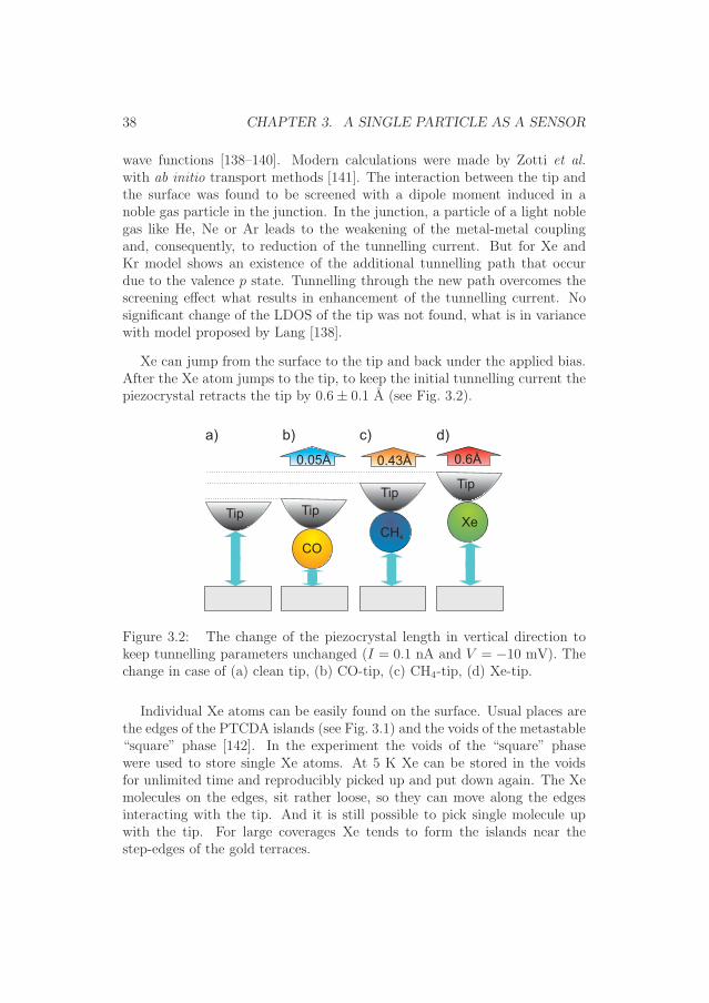
Xe can jump from the surface to the tip and back under the applied bias.After the Xe atom jumps to the tip, to keep the initial tunnelling current thepiezocrystal retracts the tip by 0.6± 0.1 A (see Fig. 3.2).
Tip
Tip
XeCH4
0.6Å
Tip
CO
0.43Å
Tip
0.05Å
a) b) c) d)
Figure 3.2: The change of the piezocrystal length in vertical direction tokeep tunnelling parameters unchanged (I = 0.1 nA and V = −10 mV). Thechange in case of (a) clean tip, (b) CO-tip, (c) CH4-tip, (d) Xe-tip.
Individual Xe atoms can be easily found on the surface. Usual places arethe edges of the PTCDA islands (see Fig. 3.1) and the voids of the metastable“square” phase [142]. In the experiment the voids of the “square” phasewere used to store single Xe atoms. At 5 K Xe can be stored in the voidsfor unlimited time and reproducibly picked up and put down again. The Xemolecules on the edges, sit rather loose, so they can move along the edgesinteracting with the tip. And it is still possible to pick single molecule upwith the tip. For large coverages Xe tends to form the islands near thestep-edges of the gold terraces.

3.2. EXPERIMENT 39
Time [sec]0 1 2 3
0
-10
-20
-30
-40
-50
I [n
A]
dista
nce
[Å]
Time [sec]0 1 2 3
0
20
40
60
80
I [n
A]
volta
ge
[V]
0
0.2
0.4
0.6
0.8
0
0.5
1
1.5a)
b) z = 0Å
U = -10mV
Figure 3.3: (a) Picking up a Xe atom. Approaching procedure of the tip(red line) and response of the current (black line) (b) Putting down Xe inthe void. Voltage variation procedure (red line) and current response (blackline). Jump in the current denote the moment when Xe jump to (a) or from(b) the tip.
The first experiments with single Xe atom manipulation were performedby Eigler and Schweizer [136]. It has been shown that Xe can be successfullypicked up from the Ni(110) surface and placed back with STM tip. Thepicking up procedure described by them was adapted in the current workfor picking up Xe from the Au(111) surface. It was taking into account thatAu(111) is less attractive than Ni(110). In the present work the tip has beenmoved from the stabilisation point (bias −10 mV, current 50 pA) towards theXe on the surface, for a distance of ≈ 1.6 A, until Xe spontaneously jumps tothe tip. In case of the Xe jump, the STS spectra show abrupt increase of theconductance, see Fig. 3.3(a). To put Xe back on the Au(111) surface or in thevoid of the “square” phase of PTCDA, we apply the potential of−0.8 V to thejunction [143]. The STS spectra show an abrupt decrease of the conductance(see Fig. 3.3(b)). Thus, the STS spectra can be used to monitor the processof Xe transition from the surface and back to the tip. The additional control

40 CHAPTER 3. A SINGLE PARTICLE AS A SENSOR
was carried out by rescanning the surface and checking if Xe is still on thesurface. The described protocol of the Xe atom manipulation is reliable andreproducible. This allowed us to study the imaging properties of STM tipsdecorated with a single Xe atom systematically.
Figure 3.4: PTCDA/Au(111). The change of the contrast before (left) andafter (right) the atom of Xe was picked up from the void. In case of scanimage made with Xe on the tip the edges of PTCDA molecules looks sharper.The images are recorded in the constant current regime. The current flowvalue is shown by the colorbar.
The images of molecules, recorded by scanning in the constant currentregime with the Xe on the tip apex, show the slight change in the contrast.The edges of the molecules are sharper (see Fig. 3.4) [139]. The currentand the conductance images, recorded very close to the surface in the con-stant height regime, show the similar contrast as in the H2 (D2) case. Thegeometrical structure of the molecules is visible (Fig. 3.5). However, the Xe-decorated tip shows poorer contrast of the intramolecular geometry structureof PTCDA than the H2 decorated tip. Nevertheless, the preparation of theXe-sensor is explicit and better controlled than preparation of H2- or D2-sensors [118].
As an other example the internal geometry structure of a copper phthalo-cyanine (CuPc) molecule on Au(111) was successfully resolved with Xe onthe tip. The experiment with CuPc molecules is sophisticated because themolecules are mobile on Au(111) and do not stick to the Au(111) substrateas good as PTCDA molecules. Due to the interaction with the tip, CuPc canfollow the tip along the surface. To obtain an image of CuPc, the moleculewas pinned to the edge of PTCDA island where the mobility of CuPc is re-duced significantly due to the interaction with the edge of PTCDA island.

3.2. EXPERIMENT 41
Figure 3.5: The image of PTCDA/Au(111), recorded in the constant heightregime with Xe modified tip. The image shows geometrical structure ofthe PTCDA molecule similar to that obtained in STHM experiments. Thecontrast in case of Xe is poor but the geometry of the molecule is visible.The current flow value is shown by the colorbar.
The geometrical contrast on the CuPc molecule is displayed in Fig. 3.6. Toget a better view of tiny details, it is shown as 3D plot.
Figure 3.6: Images of a single CuPc molecule at the edge of the PTCDAisland on Au(111), obtained in the constant current regime (left) and in theconstant height regime (right). For better view the contrast and the innertiny structure, it is plotted as a 3D surface. The current flow value is shownby the colorbar.
Another experiment with Xe was performed with PTCDA/Ag(110), wherethe structure of the PTCDA overlayer is completely different. On Ag(111),the structure is mainly “herringbone”, which is very close to the [1 0 2]plane of a bulk structure of the PTCDA crystal. This happens because theintermolecular interactions are much stronger than the interactions betweenthe molecules and the surface [132]. On Ag(110), molecules of PTCDA formcommensurate “brickwall” phase [144, 145] for the coverage less than 1 ML[146]. The interaction between the molecules and the surface is stronger

42 CHAPTER 3. A SINGLE PARTICLE AS A SENSOR
than between the neighbouring PTCDA molecules. Therefore, the PTCDAmolecules will be oriented perpendicular to the rows of the silver atoms,with the central C6 ring located between the atomic rows [144]. Due tothe interaction between the negatively charged anhydride groups and thepositively charged perylene cores, PTCDA molecules form rhombic islandswhere the negatively charged anhydride groups face each other. These placesare additionally preferable for Xe atoms, where they can be found easily. TheXe atoms adsorb above the adjacent anhydride groups, see Fig. 3.7(a), andcan easily switch between neighbouring positions 1 and 2. The jump toanother adjacent anhydride groups position is restricted by the interactionwith the PTCDA molecules.
A scan of PTCDA/Ag(110) recorded with Xe sensor is displayed in Fig.3.7(b). The scan is recorded in the constant height regime and shows theSTHM-like geometrical contrast where is possible to recognize the perylenecore with the bright central ring. It is observed a drop of the current wherethe C-C bond between adjacent C6 side ring is, but in fact it is very subtle.Nevertheless, it is possible to see it in the current profile across these tworings in Fig. 3.7(c), where the dip and its position on the scan is markedwith the red arrow. Difference in the STHM-like contrast can be dueto the structure of the Ag(110) surface that has rectangular unit cell andis more attractive than Au(111) surface. PTCDA molecules are orientedperpendicularly to the rows of sticking out Ag atoms. The central C6 ring ofPTCDA is located above one of the row. Side C6 rings are in average fartherfrom the surface. Due to the strong interaction between PTCDA moleculeand Au(111) surface geometry and electronic structure deviates from the freemolecule form [147,148]. Due to these reasons the conductance of the centerC6 rings can be higher then the side C6 rings.
3.2.2 Carbon monoxide
The next gas which was used for experiments was carbon monoxide. Pre-viously it was reported that CO was used in AFM experiments for tip func-tionalization to get high resolution of the molecules [149, 150]. The AFMexperiments have shown that it is possible to recover the structure of themolecule measuring the frequency shift of the dynamic AFM sensor. Scansof the organic molecules reveal the geometrical structure which looks similarto the structural formula from chemical books. Authors Gross et al. ascribethe contrast obtained with such tip to repulsive Pauli force [149]. Temirov etal. have linked STHM contrast also to the Pauli repulsion [118]. Therefore

3.2. EXPERIMENT 43
10Å10Å
a) b)high
low
high
low
12
2 4 6
I [a
.u.]
distance [Å]
c)
Figure 3.7: PTCDA/Ag(110), “brickwall” phase. The scan images are madewith Xe on the tip: (a) Image made in constant current regime. Xe moleculesits above adjacent anhydride groups and can switch from position 1 to 2under the interaction with the tip. (b) Image made in the constant heightregime, (set point 50 nA, 50 mV, voltage applied to the junction -10 mV).(c) Current profile along the dotted line across the double C6 rings (see inlayfigure), the dip in the conductance is shown with the red arrow. Dip positioncoincide with the location of C-C bond.
the next logical step is to check whether CO can be used to get STHM-likegeometrical contrast. This would confirm this aspect of STHM imaging.
The CO molecules present in every vacuum chamber as a rest gas, so it ispossible to find them on the surface. In the experiment for the reasons of clar-ity CO was deposited on the freshly prepared system in amount of ∼0.01 ML.The CO molecules sit on the Au(111) surface in the on-top sites and are ori-entated perpendicular to the surface with carbon end down [151, 152]. Asingle molecule of CO is visible with STM and has a distinct appearancethat makes it easy to distinguish on the surface: CO molecule appears as

44 CHAPTER 3. A SINGLE PARTICLE AS A SENSOR
depression independent of the polarity when they are scanned with a cleanSTM tip [151, 153]. CO appears as protrusion independently of the bias ifit is imaged with a tip with another CO molecule at its apex (see Fig. 3.8).Single molecules of CO located mainly on elbows of 22×
√3 Au(111) recon-
struction [130]. Owing to the change of the surface structure between fccand hcp, the elbows of the gold reconstruction are attractive to the adatomsof the different contaminations including CO molecules.
Figure 3.8: CO on Au(111), CO molecule looks like a black blob sits on theelbow of reconstruction. (a) two CO molecules scanned with clean tip. Beforeupper one is picked up. (b) CO molecule scanned with the CO-terminatedtip. CO on the surface appears as protrusion.
The deattachment of the CO molecule occurs due to the temporary tun-nelling electron injected into a 2π∗ antibonding state of CO, which leads tothe breakup of the bond between CO and the surface [151, 152, 154]. Theexcited CO molecule can jump either to a nearby atom on the surface ortowards the tip. Our experiments show that CO jumps to the tip with avery high probability which is in agreement with paper reports.
The molecule of CO can be picked up in controllable and reproducibleway [151]. To pick up CO from Au(111), the tip was positioned above it andthe bias of 2 V was applied between the tip and the sample. The initial setpoint of the tip was defined with I = 50 pA, V = −10 mV (see Fig. 3.9). Thechecking, whether the CO molecule is on the tip, is made visually by scanningthe position of the picked up CO. The quality of the tip was checked bymeasuring a molecule of CO that sits on the surface with the CO decorated

3.2. EXPERIMENT 45
Figure 3.9: Picking up the CO. Approaching procedure of the tip (red line)and response of the current (black line). The step in the current denotes themoment when CO jumps on the tip.
tip. The control of the CO jump by spectra is complicated because thetransition of CO molecule from the surface to the tip does not change stronglythe conductance of the junction. Ideally a small jump in the current shouldlook like in Fig. 3.9, but in many cases this jump was not observed, althoughthe CO molecule jumps actually to the tip. The tip is retracted from thesurface in average by ≈ 0.05 A when CO molecule comes in the junction(see Fig. 3.2). After one CO molecule is picked up, the contrast of the scanrecorded in the constant current regime changes. CO on the surface obtainsa characteristic bright spot (protrusion) in a dark ring (Fig. 3.8) [151].
Figure 3.10: PTCDA/Au(111) scanned in the constant height regime withCO on the tip. Perylene core is visible as 5 blobs corresponding to the C6
rings.

46 CHAPTER 3. A SINGLE PARTICLE AS A SENSOR
The CO modified tip yields better contrast resolution of the perylene coreof PTCDA than the Xe modified tip. Also the C6 rings of perylene corehave a specific round shape. The two C5O heterorings located at the ends ofthe molecule are not resolved as good as in case of the Xe. The specific COcontrast remains when molecules other from PTCDA species were scanned.An example of the scan image of TTCDA/Au(111) is presented in Fig. 3.11.
Figure 3.11: TTCDA/Au(111) scanned in the constant height regime withCO on the tip. The white blobs are corresponding to the C6 rings of theTTCDA core.
CO-sensors are characterized by a high stability with respect to bias ap-plied to the junction. The dI/dV image of PTCDA/Au(111) is shown inFig. 3.12(a). This scan image was recorded at the bias V = −1.6 V using thelock-in techniques. At −1.6 V it is a position of HOMO of the PTCDA onthe Au(111) substrate. At the same bias voltage, the dI/dV image recordedwith the clean tip shows contrast (Fig. 3.12(b)) related to the HOMO ofPTCDA. The comparison of two images in Fig. 3.12 (a) and (b) shows thatthe STHM contrast is not just an enhancement of the conventional LDOSresolution that derives from molecular electronic resonances. However, theSTHM contrast is affected by the sample LDOS what makes the central ringappears dark, because the HOMO has a node there, two mutually perpen-dicular nodal planes perpendicular to the plane of molecule intersect there.
3.2.3 Methane
The next series of experiments were performed with methane (CH4), be-cause the methane molecule has right tetrahedron form with four hydro-

3.2. EXPERIMENT 47
Figure 3.12: PTCDA/Au(111), (a) dI/dV image made with CO on the tipat −1.6 V. (b) Image of HOMO of PTCDA made with clean tip at −1.6 V.Inlay: model of HOMO.
gens in the corners. One corner of tetrahedron would point towards surface,whereas the other three interact with the tip and, thus, stabilize the con-figuration of the molecule. Because of the tetrahedron form the orientationof CH4 on the tip can be quite different which can bring variation in con-ductance of the junction and in the structure of the obtained image of thesurface. It is possible that one hydrogen atom sticks out or two atoms stickout. This case is similar to the orientation of hydrogen on the tip. In exper-iments CH4 was picked up randomly, without any control of the orientation.No dependence on the orientation of CH4 in the junction was revealed.
The melting temperature of methane is 91 K. A single methane moleculeis weakly bounded to the Au(111). Due to the high mobility on the surfacethe difficulties associated with methane were similar as in case of hydro-gen or deuterium. Individual CH4 molecules can be found in the voids of the“square” phase of PTCDA/Au(111) where they spontaneously adsorb duringthe deposition. The observation of the CH4 on the edges of islands is com-plicated because of the high mobility of the methane. Single CH4 moleculecannot be picked up reproducibly from the voids with the STM tip as it isin case of Xe or CO. Therefore, larger quantities of CH4 have to be adsorbedon the surface. Nevertheless, for methane the evaluated coverage was lessthan 1 ML. The preparation procedure of the CH4 sensor is thus very similarto the recipe used for obtaining STHM junctions with H2 or D2 [80], CH4
spontaneously jumps to the tip during the lateral scanning.
For the CH4 the submolecular resolution of the organic molecules wasobserved as in the previous cases. The structure of the image is similar toSTHM contrast but the intermolecular contrast is not as pronounced as in

48 CHAPTER 3. A SINGLE PARTICLE AS A SENSOR
case of hydrogen. The contrast in case of the CH4 is like the contrast obtainedwith Xe on the tip.
Figure 3.13: PTCDA/Au(111). The tip decorated with CH4 molecule demon-strates geometrical structure of the surface similar to the STHM-like contrast.
3.3 Discussion
The experiments with PTCDA/Au(111) showed that the CO-, Xe-, CH4-sensors can successfully reveal the structural contrast of the molecules de-posited on the metal substrate. The obtained images had a corrugationpattern very similar to the structural formula of the whole molecule or atleast parts of it. At the same time the corrugation of the intermolecularcontrast changes from sensor to sensor, but the pattern related to the geom-etry of the molecule remains. The best intramolecular contrast was observedwith CO-sensor which quality is comparable or similar to the H2 sensor. Theconductance above the bond and the centre of the rings have the sharpestchange in its value for the used sensors. In case of CO the C6 rings havespecific round shape while in case of Xe and CH4 the shape is angular andis closer to the hexagonal form, as in case of H2 or D2.
In Fig. 3.14(a) the profiles of the aromatic rings recorded above thePTCDA molecule are shown. The profiles demonstrate the corrugation ofthe Pauli repulsion contrast with low conductance above bonds where elec-tronic density is larger [118]. The figure shows that the images recorded withthe Xe- and CH4-sensors are laterally distorted. The Xe and CH4 sensorsshow asymmetry in the profiles across the molecule. Also the three aromatic

3.3. DISCUSSION 49
rings along the profile have different sizes. Note, that the structure of theprofile does not depend on the direction of the scanning. This rules out afriction and slip-stick as an origin of the asymmetry, because, otherwise, thedirection of the slope will depend on the direction of scanning what will beobserved in the experiment. Asymmetry of the profile and slope presencecannot be caused by the global drift of the tip from or towards the sur-face, the drift is small in the microscope. Since the position of the imagedPTCDA molecule does not change during the scan, the observed image dis-tortions must be caused by deformations of the sensor due to the complextip shape [153, 155]. In case of CO the profile is more symmetric and theleast distorted comparing to the profiles obtained with Xe and CH4 sensors.However, the distance between the extreme points of the rings in case of COis shorter than in other cases. This can be because CO is bounded stiff tothe tip while xenon or methane sit loosely and can move on the tip [156,157].But still, it can be possible that the image is distorted because of the tilt ofCO on the tip [153, 158].
x, [Å]
2 5 8 2 7 12
x, [Å]
G [a.u
.]
a) b)
Figure 3.14: PTCDA/Au(111). Conductance profile across the molecule (a)and the bond (b). Each of the curves was divided by the factor |Gmax−Gmin|,where Gmax (Gmin) are the maximum (minimum) values of the conductancein the current curve. The resulting curves were shifted along the verticalaxis.
Xe- and CH4- sensors show intermolecular contrast which coincides withthe contrast obtained with H2 (D2) sensor. The area between the molecules
50 CHAPTER 3. A SINGLE PARTICLE AS A SENSOR
is broken up into the tiles of different sizes and conductances. The tiles withsmall conductance have three PTCDA molecules as a neighbour and havelarge size. The tiles of low conductance interchange with tiles of high conduc-tance. They are smaller and have two PTCDA molecules as a neighbour. Theedges of the tiles are in good agreement with the location of H−H bonds [142].The profile recorded across the hydrogen bonds (see Fig. 3.14(b)) shows that,in fact, all three sensors behave in a similar way and are sensitive to the dif-ference of the conductance over different points of the intermolecular area.In case of Xe- and CH4-sensors, the conductance drop is stronger above thehydrogen bond and has a kink unlike in case of CO. In case of CO, con-ductance profile varies smoothly with a small variation of magnitude in theareas where H−H bonds should be. It is hard to observe a variation at thatregion on the scan images because of the very weak contrast variation. Themechanism of hydrogen bond imaging in STHM is not yet fully understood,so the poor performance of the CO-sensor can be related to some distinctiveproperties of CO.
To understand better the variation of the intramolecular contrast betweenthe different sensors, we analysed the STS conductance spectra versus tip-surface separation distance. The conductance spectra G(z) measured in twoneighbouring points (see inset of Fig. 3.15) are shown in Fig. 3.15: over thecenter of side ring (black) and over the side carbon atom (red). All theG(z) curves plotted in Fig. 3.15 show a similar exponential dependence farfrom the surface and nonexponential behaviour at short tip-sample distances.The analogous behaviour was demonstrated earlier for the spectra made withmolecular hydrogen and deuterium in the junction [118].
Far from the surface the conductance G(z) spectra are exponential. Thedeviation from the exponential behaviour emerges at some point and in-creases with the reduction of the tip-surface distance (See section 1.5). Thesuppression of the conductance is presumably due to the depletion of theDOS in the tip caused by Pauli repulsion between the tip and the particleadsorbed at the tip apex [118]. At the distances close to the surface spectrabehaves nonexponential and show distinction in curve shape for different tippositions above the surface, The spectra measured above a carbon atom (redcurve) show larger suppression of the conductance than the spectra measuredabove a center of C6 ring (black curve) of the PTCDA backbone. This dis-tinction leads to the pattern corrugation in conductance scan images. Thefirst point where the deviation emerges marks the starting distance when theSTHM-like contrast will be observed in the scan images. STHM-like contrast,observed in the scans of the surface, happens at the very short tip-surfacedistances where the spectra are nonexponential.

3.3. DISCUSSION 51
Figure 3.15: The approach conductance spectra measured above PTC-DA/Au(111) from the stabilization point: I = 50 pA, V = −10 mV. x-axisshows the relative distance between the surface and the tip. The curves wereshifted along the z-axis such that the tip-surface distances, at which the Fig-ures 1d, 2c, and 2g were scanned, coincide. For visual clarity the curves ofCH4 and CO were multiplied by 0.1.
The tip-surface distance at which the geometrical contrast is observableis different for three sensors. The sensitivity range, R, was introduced forthe sensor characterization. One endpoint of R-range is defined by the tip-sample distance where the first deviation from the exponential behaviouroccurs. Another endpoint is the tip-surface distance at which the maximumdifference in conductance values over the atom and over the center of the C6
ring is observed. Sensitivity range, R, shows how deep it is possible to probethe space under the tip (see Fig. 3.16). In case of Xe the sensitivity range islarger than in case of CO. According to Fig. 3.15, RXe > RCH4
> RCO. This

52 CHAPTER 3. A SINGLE PARTICLE AS A SENSOR
Tip
CO
Xe
RCO
Rxe
Tip
Figure 3.16: Sensitivity range defines how deep it is possible to probe thespace under the tip. In case of Xe the sensitivity range is larger than in caseof CO. This corresponds to the fact that with the Xe intermolecular andintramolecular contrast are observed while in case of CO only intramolecularcontrast is presented.
means that the Xe- and CH4-sensors produce detectable output in a widerrange of tip-surface distances, while the sensitivity of the CO-sensor decaysfaster as the tip is moved away from the sample surface.
3.4 Conclusions
In this chapter it has been shown that the STM tip with a single CO orCH4 molecule or with a single atom of Xe creates a single particle sensorthat simultaneously performs the function of an atomic-scale force sensorand a signal transducer, which couples the short-range force acting on thetip to the tunnelling conductance of the junction. These sensors have suc-cessfully resolved the inner structure of large organic molecules like PTCDAand CuPC and have shown the scan image contrast is related to the geomet-rical structure of the molecule. The scan image contrast have similar patternfor all different gas particles used in experiment. Therefore, the mechanismof the submolecular geometrical contrast formation does not depend on thedetails of the sensor particle or its interaction with a tip. This points outthat it should be a general physical phenomenon. Experiments with Xe and

3.4. CONCLUSIONS 53
CO have shown explicitly that only one molecule or one atom is needed tocreate the molecular force sensor. Therefore, one can conclude that in caseof H2 or D2 also only one molecule on the tip apex should play role for sensorformation but not a molecule on the surface under the tip. To get the STHMcontrast hydrogen molecule jumps and sticks to the tip, what happens dur-ing the motion of the tip above the surface. The area where the sensor wascreated and where it was used for scanning are spaced far on the surface whatexcludes the situation when the tip “drags” the particle along the surface.During dragging the particle will be lost because of the numerous defectsand the terraces on the surface. Therefore, the single particle sensor reallyconsists of the single molecule of the gas attached to the tip apex.
The studies of the PTCA molecules on different substrates show commonpattern of the geometrical contrast, however, slight variations are observed inthe contrast. The substrates of Au(111), Ag(111) or Ag(110) have differentmorphology and physical properties that affect the electronic structure of thePTCDA molecules and shift the position of the HOMO and LUMO of thePTCDA molecule. The full contrast observable in experiments with singleparticle sensor has variations due to the different electronic structure of themolecules but the geometrical pattern, ascribed to the geometrical structureof the molecule, remains and is the same for all the crystal surfaces.
For sensor characterization the parameter R, sensitivity range, was intro-duced. Sensitivity range determines how deep the sensor can probe the spaceunderneath it. The CO-sensors have the short sensitivity range, while Xe-or CH4-sensors have large sensitivity range. The sensors with large R showpoor contrast for the intramolecular area and matching contrast of the inter-molecular area related to the hydrogen bonds. Sensors with small R worksin the opposite way, they show poor structure of the intermolecular area, butthey show intramolecular contrast of good quality. H2 and D2, as well as Xe,are able to resolve the intermolecular structure, therefore, the sensors madewith H2 or D2 presumably should have large sensitivity range.

54 CHAPTER 3. A SINGLE PARTICLE AS A SENSOR

Chapter 4
Calibration of the atomic-forcesensor
4.1 Introduction
The STM tip decorated with a single molecule of CO or CH4 or with asingle Xe atom acts as a molecular force sensor. The action of that sensoris similar to the cases of H2 or D2 which were reported earlier [80]. Suchsensors were suggested to be able to change the tunnelling current in responseto the forces acting from the surface. Therefore, an image of the tunnellingcurrent variation, recorded with the tip in a constant height, reflects the Paulirepulsion effect from atoms. The image of the surface shows the structureof the surface. For molecules deposited on the surface, the image will reflectthe structure of the molecules. The structural resolution of the moleculeson the surface was obtained independently using an AFM sensor with COdecorated tip [93, 149, 159]. Gross et al. [149] have shown direct observationof Pauli repulsion from atoms. These two observations point out that thereis dependence between the force acting on the sensor and the tunnellingcurrent.
Current studies show that STHM contrast is related to the force acting onthe tip and therefore, it is possible to calibrate the signal in the conductancechannel in terms of force. For calibration, it is necessary to separate theeffect of the force acting on the sensor from all other factors influencing theconductance. The force cannot be tuned by simply changing the tip-surfacedistance, because in such cases the tunnelling current follows the changes ofLDOS. In experiment, the PTCDA molecule itself will be used as a force
55

56 CHAPTER 4. CALIBRATION OF THE ATOMIC-FORCE SENSOR
source. It has been shown that planar organic molecules can be used to varythe force acting on the tip in the pN range; if the tip is at a constant distancefrom the substrate and is placed at different locations of the molecule [149].Measurements in two closely spaced points in the PTCDA molecule showthat LDOS does not vary significantly. In this case, all the variations intunnelling conductance are only due to the change of the force acting on thetip.
A combined NC-AFM/STM sensor has an advantage that it can measurethe force and conductance spectra simultaneously. STM images LDOS atthe position of the tip, where the tip is far above the molecule. So the tipprobes not only a molecular orbital in its exponential tail, but also the tail ofmetal states that may leak through the molecule and blur the resulting pic-ture. AFM relies on the force measurements. To image the atomic resolutionthe tip should be moved very close to the object of study. Here the AFMsensor is in a regime where short-range forces give the main contributions.Pauli repulsion is responsible for the atomic resolution, while van der Waalsand electrostatic forces add only a diffuse attractive background [149]. Thisproblems can be partially solved with a reduced contribution of the long-range forces by using FM-AFM and the force gradient measuring. The forcegradient in the proximity of the surface depends mainly on rapidly varyingshort-range forces, while long-range forces vary rather slowly, and so can beneglected in FM-AFM. Additionally, at small distances, the results of mea-surements are affected by an influence of the exact atomic tip geometry andunintended lateral and vertical movement of the molecules. The functional-ization of the tip with an atom or a molecule allows the reactivity of the tipto be reduced and therefore, the tip can move closer to the surface.
Using a combined NC-AFM/STM sensor the tunnelling current and thefrequency shift were measured simultaneously at different tip-surface dis-tances. This information was used to reconstruct the force and conductancespectra as a function of the proximity to the surface. These spectra wereanalysed for the possibility to calibrate the sensor. As the relation betweenthe force and the conductance is known, it is possible to use an STM tip as amicroscopic force sensor when a molecule or an atom is attached to its apex.
The results of this chapter have been published in paper: G. Kichin,C. Wagner, F. S. Tautz, R.Temirov. Calibrating atomic-scale force sensorsinstalled at the tip apex of a scanning tunneling microscope. Physical reviewB, 87:081408, 2013.

4.2. EXPERIMENT 57
4.2 Experiment
An experiment was performed with NC-AFM/STM in UHV conditionsat 5 K. A test system was chosen as PTCDA/Au(111). The preparationof PTCDA/Au(111) is described in section 2.3. Above the monolayer of
“herringbone” phase of PTCDA was chosen an area 13×13 A2containing one
molecule. The probing of the surface was made with the qPlus sensor [114]with PtIr tip (see Fig. 2.4). Preparation of the tip is described in section 2.6.2.The operational oscillation frequency of the qPlus sensor was f0 = 30.3 kHz.During the measurements, the amplitude of the sensor’s oscillation was keptconstant at ≈ 0.2 A [160]. Constant height scan images were made withsmall tunnelling bias V = −12 mV applied to the junction.
Three different types of tips were used: a clean Au tip, an Au tip decoratedwith a single CO molecule and an Au tip decorated with a single Xe atom.Sequences of images with frequency shift (∆f) and conductance (dI/dV )were recorded simultaneously at various tip-surface distances with a step of0.1 A. Spectra of frequency shift (∆f(z)) and conductance (dI/dV (z)) wereextracted from the sequence of scanned images. For calibration spectra twoparticular positions on the molecule were chosen. One spectrum of interestwas obtained for the central point of the central C6 and the other abovethe nearest carbon atom, indicated by the blue and red circle in Fig. 4.1(a).These two points are located ≈ 1.4 A from each other. For these two points,force and conductance spectra have been obtained. Force spectra, F (z), wereobtained by integrating frequency shift spectra over the measured range ofdistances,
F (z) =
z∫
0
2k0f0
∆f(z)dz, (4.1)
where k0 = 1800 N/m is the fork stiffness of the qPlus sensor and z = 0 is themaximal distance from the surface, at which the scan image was recorded. zincreases as the tip approaches the surface. For large tip-to-surface distances,no corrugation in image contrast was observed [161].
A sequence of images recorded with a clean Au tip shows featureless con-trast without any internal structure of the molecule at any distance (Fig.4.1(a)). Spectra extracted above the ring and above the atom (see Fig. 4.1(b))are identical, so
Fatom(z) = Fring(z) (4.2)
anddI/dVatom(z) = dI/dVring(z). (4.3)

58 CHAPTER 4. CALIBRATION OF THE ATOMIC-FORCE SENSOR
10
00
0
01
00
00 1 2 3 4
z, [Å]
F, [pN
]
dI/dV, [n
S]
(b)
(a)
dI/dV
Δf
dI/dVatom= dI/dVring
Fatom = Fring
-45
-32 -50
-85
HzHz
-26
-23
Hz
77
10
416
50
562
66
nS nSnS
Figure 4.1: (a) 13 × 13 A2constant height ∆f (top) and dI/dV (bottom)
images from the image sequence of PTCDA/Au(111) measured at differentheights with the clean Au tip. The chemical structure formula of PTCDA isshown in the tile, red and blue circles mark the positions at which F (z) anddI/dV (z) were evaluated. (b) Force F (z) (top) and conductance dI/dV (z)(bottom) spectra extracted from the image series (a). Spectra were measuredover the atom (red curve) and over the middle point of central C6 ring. For Fscale negative (positive) value corresponds to an attractive (repulsive) force.
LDOS of PTCDA does not deviate significantly between these two locations.Force F (z) spectra in Fig. 4.1(b) show that clean Au tip is quite reactive.The tip senses a strong attraction toward the surface [162]. At z ≈ 3 A,white patches on the ∆f image show local interaction of the tip with thecorner oxygens of PTCDA. This points out the chemical nature of the at-traction. The corner oxygen flips up and tries to form a chemical bond withthe tip [163]. As the tip approach further towards the surface, the interactionincreases and destabilizes the junction.
Unlike the clean tip, a tip with attached CO molecule is able to showthe internal molecular structure of PTCDA in both ∆f and dI/dV channels
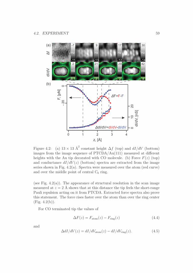
4.2. EXPERIMENT 59
20
0
01
020
0 1 2 3 4d
I/d
V,
[nS
]
F, [
pN
]
z, [Å]
(b)
(a)
ΔF= -F F
ΔdI/dV= -dI/dV dI/dV
dI/
dV
Δf
-12
17 30
-14
HzHz
-11
-7
Hz
-13
9
Hz
2
0.1
21
2
29
2
42
4
nS nSnSnS
Figure 4.2: (a) 13 × 13 A2constant height ∆f (top) and dI/dV (bottom)
images from the image sequence of PTCDA/Au(111) measured at differentheights with the Au tip decorated with CO molecule. (b) Force F (z) (top)and conductance dI/dV (z) (bottom) spectra are extracted from the imageseries shown in Fig. 4.2(a). Spectra were measured over the atom (red curve)and over the middle point of central C6 ring.
(see Fig. 4.2(a)). The appearance of structural resolution in the scan imagemeasured at z = 2 A shows that at this distance the tip feels the short-rangePauli repulsion acting on it from PTCDA. Extracted force spectra also provethis statement. The force rises faster over the atom than over the ring center(Fig. 4.2(b)).
For CO terminated tip the values of
∆F (z) = Fatom(z)− Fring(z) (4.4)
and∆dI/dV (z) = dI/dVatom(z)− dI/dVring(z). (4.5)

60 CHAPTER 4. CALIBRATION OF THE ATOMIC-FORCE SENSOR
show distinct variation with tip-surface distance. Far from the surface (z = 0)∆F (z) = 0. This value grows as the tip approaches the surface, reaching amaximum value at the distance z ≈ 2.2 A. Here ∆dI/dV (z) is negativeand keeps decreasing with the tip approach. Spectra show that junctionconductance drops with an increase of the force acting on the tip. Closeto the surface, at distances z & 2.3 A, the value of ∆F (z) starts to becomenegative. Inversion in ∆f happens at smaller z′ values (z′ < z), which followsfrom Eq. 4.1. In the spectra we observe a change of sign for ∆F (z) and ∆f .In the frequency shift scan images, this effect leads to the contrast inversion(see Fig. 4.2). Far from the surface C-C bonds are bright and the rings aredark. Frequency shift for tip positioned above the rings is smaller than overthe atoms and bonds (see Fig. 4.2). For z > 2.2, the frequency shift ∆f abovethe ring become larger than over the atoms or bonds. At the same z ≈ 2.2,∆dI/dV (z) shows a weak response to the change in tip-surface interaction,which can be due to different types of tip-surface interaction. The emergenceof an attractive force cannot be described with a simple two particle Lennard-Jones type potential. The emerged attraction can be due to the complicatedstructure of the junction that has a large number of degrees of freedom, owingto the particle in the junction. For instance, lateral movement of the particlecan influence strongly on the interactions in the junction. Therefore, at shorttip-surface distances, the coupling between ∆F (z) and ∆dI/dV might havea different character of relation.
The Xe-sensor shows similar behaviour to the CO-sensor. The relationbetween ∆F (z) and ∆dI/dV have similar characteristic as in the case ofCO. The molecular structure of PTCDA starts become visible at distancesstarting from z ≥ 3.1 A. Visually the corrugation of image contrast is not asstrong as in the case of CO-tip. Thus, the difference between minimum andmaximum values of the conductance and force is larger for Xe in comparisonwith CO. Poor quality of the image resolution and spectra can be causedby several reasons. The tip with Xe is more reactive than the tip withCO (compare in Figs. 4.2(b) and 4.3(b) spectra of ∆f and ∆dI/dV ), andless reactive than the clean tip (compare in Figs. 4.1(b) and 4.3(b) spectra∆f and ∆dI/dV ). Another reason may be a small contribution of ∆f and∆dI/dV to the total signal comparable to the total signal, which makes ithard to detect. Also the tip with Xe is more sensitive to the amplitude ofqPus sensor oscillation, because of the soft Xe-tip bond. Displacement of Xein the junction adds blur to the scanned images and spectra.
Large conductance of the junction with Xe is due to the existence ofadditional tunnelling channels through the valence 5p state of Xe [141]. Thestate is broadened due to the strong hybridization with the gold states. Xe

4.2. EXPERIMENT 61
100
0
0150
300
0 1 2 3 4d
I/d
V,
[nS
]
F, [
pN
]
z, [Å]
(b)
(a)
ΔdI/dV= -dI/dV dI/dV
ΔF= -F F
dI/
dV
Δf
-11
2 20
-6
HzHz
-6
-4
Hz
-11
-7
Hz
15
2
109
7
176
9
374
19
nS nSnSnS
Figure 4.3: (a) 13 × 13 A2constant height ∆f (top) and dI/dV (bottom)
images from the image sequence of PTCDA/Au(111) measured at differentheights with the Au tip decorated with Xe atom. (b) Force F (z) (top)and conductance dI/dV (z) (bottom) spectra extracted from the image seriesshown in Fig. 4.3(a). Spectra were measured over the atom (red curve) andover the middle point of central C6 ring.
also induces a dipole moment which screens the interaction between the leads,and decrease the conductance [141]. Nevertheless, the contribution to thetunnelling through 5p state is quite large and overcomes the screening effect.This disagrees with the calculations of Ref. [138, 139], where the calculatedelectron transport through Xe was found to occur through the tail of the 6sorbital.

62 CHAPTER 4. CALIBRATION OF THE ATOMIC-FORCE SENSOR
4.3 Discussion
∆F (z) and ∆dI/dV (z) are used to characterize the conductance responsein the acting force. To get a relation between ∆F (z) and ∆dI/dV (z) (seeEq. 4.4 and 4.5) these two values are plotted versus each other (see Fig. 4.4).Far from the surface at z = 0 the proportionality between ∆F (z) and∆dI/dV was found to be linear. Linear proportionality was found in dif-ferent experiments, where the tip was freshly prepared and decorated withthe same type of particle. The linear proportionality was observed up to themoment when ∆F (z) changes its sign. The coefficient of proportionality forXe was found equal to αXe ≈ −2000 S
Nand for CO equal to αCO ≈ −200 S
N.
Thus, relation between force and conductance can be unambiguously definedas linear with a single proportionality constant.
ΔdI/dV, [n
S]
ΔF, [pN]
ΔdI/dV, [n
S]
ΔF, [pN]
Xe tip2
Xe tip1
CO tip2
CO tip1
80 60 40 20 0 20
4.5
31
.50
30 20 10 0 10
30
15
0
z=0 Å
z=2.2 Å
z=2.2 Å
z=0 Åz=2.7 Å
z=2.6 Å
Figure 4.4: Conductance response ∆dI/dV vs the applied force ∆F (z). Theupper (lower) panel shows spectra measured with two different CO (Xe) tips.The regime in which the response of conductance is linear is indicated by theblack fitted lines. The distance at which each tip starts to deviate from thelinear response regime is marked on the right.
The linear regime violates near the point where ∆F (z) changes its sign.It happens at short tip-surface distances, when the attractive force acting onthe tip from the side of the surface dominates the interactions in the junc-tion. In the non-linear regime, the coupling between ∆F (z) and ∆dI/dV (z)seems tip-dependent. The particle in the junction starts to behave in a com-plicated way. Nevertheless, for all investigated tips, coupling behaviour was

4.3. DISCUSSION 63
found qualitatively similar (Fig. 4.4). Remarkably, the inner structure of thePTCDA molecule is observed on a large range of z-distances even when thecoupling is not only in linear but also in non-linear regimes.
Interestingly, the hydrogen bonds in intermolecular area of the STHMcontrast, happens only at z-distances, where the sensor is in the non-linearregime [142,164]. Xe and CO STHM-like contrast with observable intermolec-ular structure is shown on rightmost tile in Fig. 4.3(a) for Xe and Fig. 4.2(a)for CO. It is possible to conclude that hydrogen bonds act in a specific wayon the sensor particle. The mechanism that is responsible for the non-linearcoupling is sensitive for this kind of action and transduces this force into theconductance channel.
These observations give us a reason to believe that for other moleculeslike H2, D2, CH4, for which STHM contrast was reported, coupling betweenforce and conductance spectra should be observed in a similar way. Thecoupling between force and conductance is expected to be in two regimes,linear and non-linear. It is assumed that the linear regime should be observedat large tip-surface distances, where the decrease of the junction conductanceis proportional to the increase of the force acting on the tip. The linear regimeis fully defined with a single proportionality constant that does not dependon the microscopic structure of the tip but only on the type of particle. Atsmall tip-to-surface distances, non-linear proportionality is expected. Themechanism standing behind the geometrical contrast formation seems to haveuniversal character and should not depend on the atomic structure of the tipor the particle attached to the tip. This follows from the fact that STHMimages are observed for different types of particles. The molecules and thesingle atoms have different structures and different bonding character to thetip (chemical or van der Waals).
A possible model of STHM contrast formation was suggested by Martinezet al. [165]. The proposed model assumes that molecular hydrogen dissoci-ated on the Au tip and the adsorbed hydrogen atoms, change the densityof states of the tip, increasing its p-orbital and reducing the s-orbital con-tribution. The interaction of the H-decorated Au tip with PTCDA/Au(111)pins the Fermi energy, EF, in the middle of the PTCDA LUMO peak andincreases the sample DOS at the Fermi energy level, which allows electronsto tunnel from or to this peak at very low bias voltages. The model relies onthe specific details of the chemical interaction between H2 and Au. Dissoci-ated H2 should make a strong bond with the tip, and therefore the energyneeded to clean the tip should be high (≈ 2 eV). This disagrees with theSTHM experiments. An energy needed to clean the tip is actually much

64 CHAPTER 4. CALIBRATION OF THE ATOMIC-FORCE SENSOR
smaller (40− 200 eV), which tells us that the molecular hydrogen should siton the tip as a whole molecule. Another reason is that hydrogen molecules donot dissociate on single crystal Ag [166, 167] and the Au surfaces [168, 169],because of the considerable activation barriers that prevent this.
The model of STHM contrast formation proposed in [80] and describedin section 1.5 has in fact a more general character. It implies that a particleadsorbed on the tip interacts also with the surface. The interaction betweenthe particle and the surface disturbs the particle and shifts its position withrespect of the tip during the scanning. In this case the position to theparticle should contain information about the interactions. If the positionof the particle changes the tunnelling current through the junction, then theforce acting on the particle is coupled to the conductance. The character ofthis coupling will be defined by the physical mechanism through which theparticle position influenced the electron tunnelling.
Currently there are two mechanisms that can possibly explain how thedisplacement of the particle on the tip can affect the conducting propertiesof the junction. According to one of them, the particle is shifted on thetip due to the interaction with the surface and is pressed into the tip. Theparticle changes the tip DOS via the Pauli repulsion acting between the tipand the particle. The conductance of the junction using the Tersoff-Hamannapproximation, is proportional to the DOS of the tip. Here the couplingoccurs due to the increased repulsion between tip and sensor particle thatdepletes the tip DOS close to the Fermi level [118].
Another possible model was proposed by van der Maas et al. [170]. Theirmodel assumes that only the electrons tunnelling in some finite solid angle Ωt
give a contribution to the tunnelling current. The atom or molecule attachedto the tip works as a shutter that reduces the number of tunnelling electronsby elastically scattering them back. The presence of the particle reduces solidangle Ωt by a value Ωs, and casts a “shadow” on the surface. Electrons inthis “shadowed” solid angle are scattered back and do not contribute to thetotal tunnelling, thus the total solid angle that contributes to the tunnellingis Ωt − Ωs. The authors proposed that the solid angle Ωt depends only onthe tip, while Ωs depends on the tip-particle distance. At large tip-surfacedistances, the particle sits at a constant position with respect to the tip andtherefore Ωs is constant. For large distances the tunnelling current dependsonly on the tip-surface separation, d, exponentially I ∝ exp(−d). At smalltip-surface separations, the second effect take place, the particle starts tointeract with the substrate and is pushed into the tip. Due to this shift Ωs
is increased and, consequently, the total angle Ωs − Ωt is decreased . Non-
4.4. CONCLUSIONS 65
linearities will be observed in the conductance spectra. In the case when thesecond effect is strong, the resulting tunnelling current will decrease as thetip approaches the surface.
Both models predict that the increase of the force pressing on the tipwill lower the junction conductance. That is in qualitative agreement withexperiments. Unfortunately, experiments cannot give a distinction betweenthese two models. Quantitative computer simulations of the coupling arenecessary for further discrimination between these two models.
4.4 Conclusions
The experiments have shown that an interrelation between conductance ofthe junction and force acting on the tip exists. At large distances between thetip and the surface interrelation has a linear dependence. The linear regimeis stable and reproducible. The coefficient of proportionality α depends onthe type of a particle attached to the apex of the tip, but not on the details oftip’s or particle’s atomic structure. For Xe sensor we found αXe = −2000 S
N
and for CO sensor αCO = −200 SN, where the minus sign shows that the
conductance of the junction decreases with an increase of the force acting onthe tip.
At short tip-surface distances the linear regime violates. The force-con-ductance relation starts to depend on the shape of the tip. The interrelationfor non-linear regime was found qualitatively to be identical in different ex-periments. This approach shows that it is possible to reconstruct force fromthe conductance. For further study numerical calculations should be per-formed where the form of the tip is taken into account.
The geometrical contrast of the molecule is observed in conductance scanimages at the distances where the sensor works in the linear regime andpartially in the non-linear regime. The STHM-like intermolecular contrastis observed only in a deep non-linear regime, when the tip is very closeto the surface. In case of D2, H2, CH4 similar relation between force andconductance is also expected. With such sensors it is possible to obtainstructural resolution of the surface with little effort and without additionalequipment.

66 CHAPTER 4. CALIBRATION OF THE ATOMIC-FORCE SENSOR
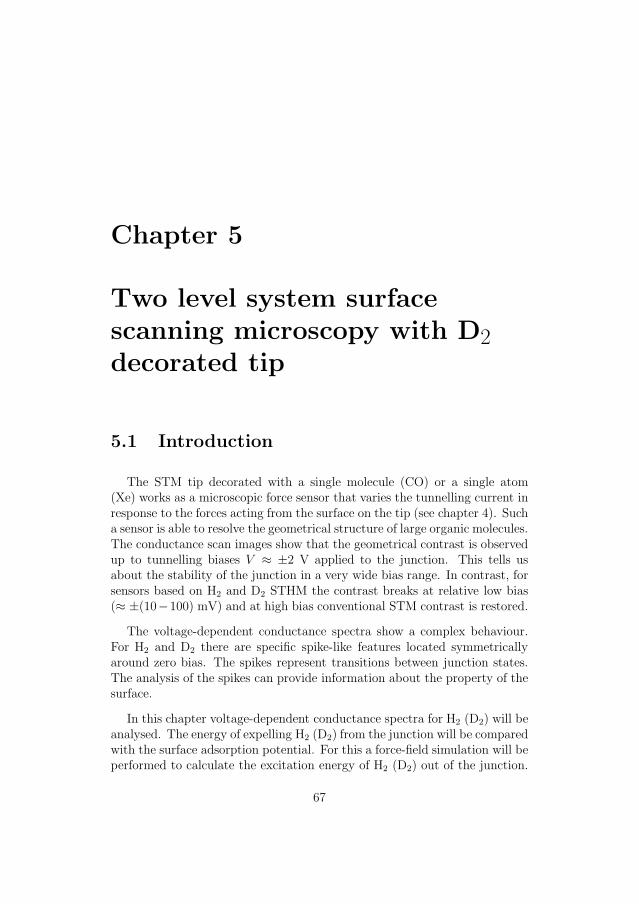
Chapter 5
Two level system surfacescanning microscopy with D2
decorated tip
5.1 Introduction
The STM tip decorated with a single molecule (CO) or a single atom(Xe) works as a microscopic force sensor that varies the tunnelling current inresponse to the forces acting from the surface on the tip (see chapter 4). Sucha sensor is able to resolve the geometrical structure of large organic molecules.The conductance scan images show that the geometrical contrast is observedup to tunnelling biases V ≈ ±2 V applied to the junction. This tells usabout the stability of the junction in a very wide bias range. In contrast, forsensors based on H2 and D2 STHM the contrast breaks at relative low bias(≈ ±(10−100) mV) and at high bias conventional STM contrast is restored.
The voltage-dependent conductance spectra show a complex behaviour.For H2 and D2 there are specific spike-like features located symmetricallyaround zero bias. The spikes represent transitions between junction states.The analysis of the spikes can provide information about the property of thesurface.
In this chapter voltage-dependent conductance spectra for H2 (D2) will beanalysed. The energy of expelling H2 (D2) from the junction will be comparedwith the surface adsorption potential. For this a force-field simulation will beperformed to calculate the excitation energy of H2 (D2) out of the junction.
67

68 CHAPTER 5. TLS SURFACE SCANNING MICROSCOPY
The relation between H2 (D2) displacement on the tip and the conductancescan images will be discussed.
5.2 Experiment
The experiment was performed in UHV conditions at the temperatureT = 5 K. For the experiment, PTCDA molecules were deposited on theAu(111) surface. PTCDA molecules form islands with the regular structure(see section 2.3). Molecular deuterium was dosed into the STM chamber fromwhere it condenses on the sample surface. D2 does not dissociate on singlecrystal Au surfaces due to the considerable activation barriers [168, 169].
To obtain the D2 sensor, the tip was moved along the surface from whereD2 spontaneously jumps to the tip. As soon as D2 is on the tip, the newtype of contrast appears, the so called STHM contrast. The deposition ofdeuterium was stopped as soon as a stable STHM contrast was achieved.In the previous chapter it was shown that only one molecule is needed forcontrast formation, but a single D2 molecule is invisible with STM, thereforea larger amount of D2 is needed.
While the tip was moved along the surface in the constant height, a setof voltage-dependent conductance spectra was measured above an area of13× 13 A2 on a grid of 64 × 64 points. The bias voltage was varied between−200 mV and 200 mV. The tip was placed over the center of the moleculewith parameters I = 100 pA and V = 316 mV, so the initial tip-surfacedistance was set. The lock-in technique was used to measure the differentialconductance dI/dV (modulation amplitude 4 mV, frequency 4.8 kHz). Theexperiment lasted 4 hours with switched off feedback. In the experiment,the total z-drift was 0.3 A, which shows the high stability of the measuringequipment.
A typical spectrum recorded with a clean metal tip shows a smooth con-ductance curve without any peculiarities (see Fig. 5.1(a)). The spectrum waschanged if the molecular deuterium sat on the tip. The dI/dV (V ) spectrareveal an abrupt change of the conductance(see Fig. 5.1(b)). The regionswith different conductance are separated by a pronounced gap-like featurewith an amplitude of spikes larger than the fluctuations of the signal. Thespikes arise in pairs and are located around the zero bias symmetrically at±Us, which signals an inelastic tunnelling process in the junction. The clas-sical theory of the inelastic tunnelling predicts a step-like behaviour of the
5.3. TWO LEVEL SYSTEMS 69
conductance with respect to the bias. An inelastically tunnelling channel isopened or closed (see 1.2) which leads to the changes in the conductance.Inelastically tunnelling electrons can excite vibrational modes of the molec-ular D2 and induce its motion out of the junction [171–173]. The structureof the junction changes. In our experiment at low bias, molecular D2 sits inthe junction while at high bias the junction is clean [80].
(a) (b)
Figure 5.1: Conductance spectra over the layer of PTCDA (a) with a cleantip and (b) with the deuterium in the junction. In case of D2 symmetricallylocated spike-like features are observed.
5.3 Two level systems
The conductance spectra measured with a tip decorated with H2 (D2) showspike-like anomalies. Although the spikes are regularly observed in the exper-iments with deuterium and hydrogen, the model that describes this physicalprocess is still debatable. There are two models in the literature under dis-cussion that describe the spike-like features in the conductance spectra. Bothmodels suggest that the STM junction can be in different states.
Halbritter et al. [174] proposed a two level system (TLS) with two minimalenergy states (marked with ΨL and ΨH) that are separated by a potentialbarrier (see Fig. 5.2(a)). The junction that is described with TLS has dif-ferent conductance in each state, σL in the L-state and σH in the H-state.Direct transitions between the states occur owing to the inelastically tun-nelling electrons that excite H2 (D2) in the junction. Spike-like behaviourcan occur only if there is a strong asymmetry in the coupling between thestates. The asymmetry can arise if the ground state L is non-degenerate andthe excited state H is highly degenerate. In such case, γL = NγH , whereN is the number of the degenerate H levels, γL is coupling of the electronsto the lower state of TLS and γH is coupling to the upper state. In other

70 CHAPTER 5. TLS SURFACE SCANNING MICROSCOPY
(a) (b)
Figure 5.2: (a) Schematic picture of D2 transition between the states in (a)Halbritter model and in (b) Thijssen model.
words, once the particle is inelastically excited it cannot easily relax back.In the conductance spectra, this asymmetry leads to the appearance of thespikes at ±Us. According to this model, the voltage Us is tied with the en-ergy difference between these two states [175–177]. Halbritter et al. pointout that the position of the spikes is not constant. It strongly depends onthe amount of H2 (D2) and shows a broad distribution in the energy rangeof 30− 100 meV.
In the other model, Thijssen et al. [178] suggested a similar TLS modelwith two energy minima, also separated by an energy barrier, but with adifferent mechanism of transition between the states. The transition doesnot occur directly between the states ΨL and ΨH, but through the interme-diate state Ψ∗. The H2 molecule that is in state ΨL is first excited by aninelastically tunnelling electron to the state Ψ∗. Now it has enough energy toovercome the barrier and then relaxes to the state ΨH (see Fig. 5.2(b)). Thecoupling of tunnelling electrons to both states is considered to be equal. Inthis model, the spike voltage Us is related to the energy difference betweenΨL and Ψ∗. Using molecular controlled break junctions (MCBJ) with H2,Thijssen et al. have found that the spike energy is observed near ≈ 42 meV,which relates to the transversal vibrational mode of H2 in the junction, wherethe H2 vibration is perpendicular to the current direction. Thijssen’s exper-iments show an isotope shift of the spike positions. For D2 the spike energyshifts by the factor ≈
√2 and was observed at ≈ 29 meV, as expected for
molecular vibration mode energies [179].

5.3. TWO LEVEL SYSTEMS 71
Non-linearities in the conductance spectra were studied also by Gupta etal. [180]. Metal surfaces covered with H2 were investigated with STM. Itwas found that the bias at which the spikes were observed depends on thesurface coverage of deposited H2. The experiments with H2 and D2 showthat it is not possible to distinguish between these two gases using STM.The coverage cannot be precisely measured, and therefore the dependenceof the spike position on the coverage cannot be derived. The disagreementwith results obtained with MCBJ can be due to the differences in the junctionstructure in the case of MCBJ and STM. Our experiments show that the spikeposition depends on the coverage of D2 as in case of Gupta’s experiments.Additionally, it was found that the spikes are sensitive to the surface areabeneath the tip. From our experiments, it is not possible to distinguish whichof the model, mentioned above, is preferable. We will keep to the concept ofthe two-level system where the junction can be in different states.
Our experiments show that one pair of spikes is always related to expellingof the H2 or D2 molecules from the junction. When there are two pairs ofspikes, the one at the larger bias value is related to expelling. This fact wasconfirmed by the spectra and by the scan images taken at different biases [80].The STHM contrast is observed only at the low bias, while at the high biasthe structure of the conductance images coincide with the conventional STMcontrast. The distance-dependent conductance spectra show an exponentialbehaviour at high bias and nonexponential behaviour at low bias where thescan images exhibit the STHM contrast.
The TLS model concept will be applied to the junction states to probe thesurface. In general, the parameters of the TLS model depend on the tip, onthe local surface area beneath the tip and on the state of D2 in the junction.The STM tip remains unchanged during the scanning. The states of TLS arerepresented by a junction with and without D2. Switching between the TLSlevels provides information about desorption energy potential of D2 from thesurface. Therefore, the excitation energy of D2 depends on the surface underthe tip. The excitation energy can be monitored with the voltage-dependentconductance spectra.

72 CHAPTER 5. TLS SURFACE SCANNING MICROSCOPY
5.4 Experimental results
5.4.1 Lateral dependence of conductance spectra
The spectra recorded in different points of the surface show high sensitivityof TLS on the surface properties. Above the PTCDA molecule (Fig. 5.3(b)),only one pair of symmetric spikes is observed. It shows that the junctioncan be in two states, ΨL and ΨH. The spikes at Us = Uout ≈ ±35 − 40 mVdenote D2 excitation out of the junction. The same is observed for negativebias. When the tip is above the intermolecular area (Fig. 5.3(a)), two pairs oftransitions are observed. Consequently, there are two pairs of spikes, at ±Us
and at ±Uout and three states of the junction. Actually, we are interestedin the spikes at ±Uout, since at ±Uout, the D2 molecule is expelled from thejunction. We are interested in the bias voltage needed the clean the junction.For the voltages V < |Uout|, the junction is filled. The spikes at ±Us showthat there is a process, in which the conductance of the junction changes butD2 remains in the junction. The initial low-bias state ΨL switches to the ΨM
state with different conductance.
(a) (b)
Figure 5.3: Conductance spectra measured (a) between the molecules and(b) above the molecule. Above the molecule, the junction can be in twostates. Between the molecules a third state of the junction is observed. InΨM, D2 is present in the junction. The junction is empty in both cases athigh bias (ΨH).
In Fig. 5.4 a set of the spectra measured along a line that connects thecenter of the PTCDA molecule and the middle point between two neighbour-ing molecules is presented. Only the two types of spectra that were describedabove are observed. The spectrum recorded on the border of the moleculeseparates spectra of these two types. The large noise level of the borderspectrum reflects the instability of the junction on the edge of the molecule.The shape of the spectra clearly depends on the point of the surface. Note

5.4. EXPERIMENTAL RESULTS 73
that there are also clear differences between the spectra of the same type.
Figure 5.4: Set of conductance spectra measured along the path markedwith red line. For better view all the spectra are shown with offset. The redone spectra corresponds to the point where the tip is over the edge of themolecule. Over the molecule two states of the junction are observed whilebetween the molecules there are three states.
Above the molecule, the STS spectra show only one transition at ≈ 35−40 mV, between the state ΨH and the state ΨL. D2 can easily escape fromthe junction indicating that D2 sits in a shallow potential well with a lowescape barrier. The conductance spectra measured in between neighbouringmolecules show two transitions and three states of the junction. The state ΨM
arises between the states ΨL and the state ΨH only between the molecules.In the ΨM state, D2 is still in the junction. The junction state switches tothe new state ΨM at Us = ±35− 50 mV (see below). The escape of D2 fromthe junction occurs at Uout. The values of Us do not vary significantly, whilevalues of Uout vary from 35 mV near the edge of the molecule and to 160 mV inthe middle point between molecules. This can be understood in the followingway: D2 can be pushed into the gap between the molecules, because there is aroom there. But D2 cannot be pushed into the PTCDA because the averagedistance between the atoms of neighbouring PTCDA molecules is larger thanthe distance between the atoms of the same molecule. The movement of D2
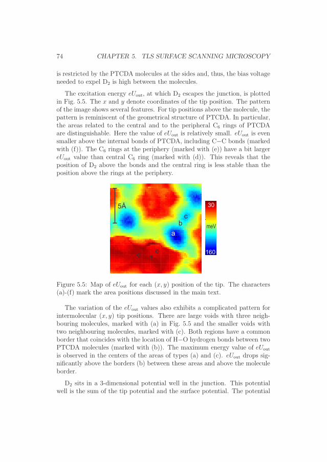
74 CHAPTER 5. TLS SURFACE SCANNING MICROSCOPY
is restricted by the PTCDA molecules at the sides and, thus, the bias voltageneeded to expel D2 is high between the molecules.
The excitation energy eUout, at which D2 escapes the junction, is plottedin Fig. 5.5. The x and y denote coordinates of the tip position. The patternof the image shows several features. For tip positions above the molecule, thepattern is reminiscent of the geometrical structure of PTCDA. In particular,the areas related to the central and to the peripheral C6 rings of PTCDAare distinguishable. Here the value of eUout is relatively small. eUout is evensmaller above the internal bonds of PTCDA, including C−C bonds (markedwith (f)). The C6 rings at the periphery (marked with (e)) have a bit largereUout value than central C6 ring (marked with (d)). This reveals that theposition of D2 above the bonds and the central ring is less stable than theposition above the rings at the periphery.
Figure 5.5: Map of eUout for each (x, y) position of the tip. The characters(a)-(f) mark the area positions discussed in the main text.
The variation of the eUout values also exhibits a complicated pattern forintermolecular (x, y) tip positions. There are large voids with three neigh-bouring molecules, marked with (a) in Fig. 5.5 and the smaller voids withtwo neighbouring molecules, marked with (c). Both regions have a commonborder that coincides with the location of H−O hydrogen bonds between twoPTCDA molecules (marked with (b)). The maximum energy value of eUout
is observed in the centers of the areas of types (a) and (c). eUout drops sig-nificantly above the borders (b) between these areas and above the moleculeborder.
D2 sits in a 3-dimensional potential well in the junction. This potentialwell is the sum of the tip potential and the surface potential. The potential

5.4. EXPERIMENTAL RESULTS 75
created by the tip remains unchanged during the scanning, while the surfacepotential varies from point to point on the surface and adds a perturbationto the initial potential well of the tip. By mapping the excitation energyalong the surface, it is possible to obtain the information related to the localadsorption potential of the D2 molecules on the surface. It is interestingto compare obtained information with the adsorption energy for the D2-likemolecules. This will be done in section 5.5. However, before we turn to thistask, we are going to construct bias dependent maps from the spectra of thepresent section and discuss the bias dependence of the imaging mechanism
5.4.2 Bias dependence of the STHM contrast
The STS spectra show that an escape of D2 from the junction occurs atUout. At the bias V > Uout the junction is empty and at the bias V < Uout thejunction holds a D2 molecule. For different points of the surface switchingoccurs at different bias voltages Uout. At some biases both types of contrast,STM and STHM contrast, should be observed in one image, depending on theposition. Rebuilding the conductance maps at the fixed biases, it is possibleto reconstruct the contrast conversion from STHM to STM. For low biasvoltage, the reconstructed images show the same type of corrugation as thescan images recorded with the corresponding bias in the constant heightregime. An example of the image taken from [142] and reconstructed imageare in Fig. 5.6). We note in passing that the possibility to reconstructSTHM images from statically measured spectra rules out a contribution ofany dynamic effects, such as friction or stick-slip, in STHM image formation.
The evolution of the conductance scan images with respect to the biasvoltage applied to the junction is shown in Fig. 5.7. At V = 5 mV thescan image shows STHM contrast (Fig. 5.7(a)) and at V = 150 mV thecontrast converts completely to the conventional STM contrast (Fig. 5.7(o)).Figs. 5.7(b)-(n) show the intermediate steps of the contrast conversion fromSTHM to STM.
At low bias, the STHM contrast is observed for intra- and intermolecularareas, D2 is present in the junction for all tip positions (see Figs. 5.7(a)-(e)). According to the spectra, the transition to the state ΨH happens earlierabove the molecules. The breaking of the STHM contrast starts at the bias ofV ≈ 30 mV at the edges of the molecules and then it propagates towards thecenters of the molecules along the bonds. Sharp lines, that denote chemicalbonds, blur and smooth out. First the central ring is blurred, the peripheralrings after. In Figs. 5.7(f)-(i) we observe the change of the contrast for the

76 CHAPTER 5. TLS SURFACE SCANNING MICROSCOPY
O
O
O
O
O
OOOO
a) b)
Figure 5.6: PTCDA/Au(111), (a) STHM image recorded in the constantheight regime, bias applied to the junction, V = -2 mV, taken from refer-ence [142]. The backbone structure of PTCDA is superimposed over thepicture. The size of the image is 1.3 nm × 1.3 nm. (b) The image of thePTCDA/Au(111) reconstructed from the set of the STS spectra discussed insection 5.4.1 at the bias of V = -2 mV.
peripheral rings. The geometrical structure of the molecules is not visibleanymore starting from the bias V ≈ 50 mV (Fig. 5.7(i)). For the positionabove the molecules the junction state is ΨH with no D2 on the tip.
The initial STHM-like contrast between the molecules is retained still atV ≥ 50 mV. According to the spectra, the junction here switches first intothe state ΨM. Thus, we can conclude that the junction in state ΨM still hasa D2 molecule in it. Between the molecules switching from the STHM to theSTM contrast is observed starting from the bias of V & 70 mV. The blurringstarts to propagate toward the intermolecular area along the hydrogen bonds(marked with yellow arrow in Fig. 5.7 (k)-(m)). We can see that the areaswith the STHM contrast are separated from the areas with the STM contrastwith borders of increased conductance (see Fig. 5.7(m)-(n)). The areas ofSTHM contrast are squeezing to the circular spots (is marked with red arrowsin Fig. 5.7(n)) until they disappear completely at V ≈ 150 mV. For the biasV & 150 mV the whole image has the STM contrast.
The conductance profiles across the molecule and intermolecular area arequite different in case of the STM and the STHM contrast. Fig. 5.8 showshow the conductance profile (marked in Fig. 5.8 left panel with a red arrow)changes with respect to the bias and how the transformation from the STHMcontrast to the STM contrast occurs. At |V | < 35 mV, the junction is in thestate ΨL and the STHM contrast is observable. The junction is in state ΨL

5.4. EXPERIMENTAL RESULTS 77
Figure 5.7: Slices extracted from the set of the conductance spectra at thedifferent biases. Each picture shows the conductance map at the distinctconstant bias. (a)-(e) STHM contrast of PTCDA/Ag(111). The geometricalpattern of the PTCDA molecules is observed. The contrast related to thehydrogen bonds is observed between the molecules. The junction is in thestate ΨL. (f)-(h) STHM-like contrast, the junction is in state ΨM above themolecules and ΨH everywhere else. (i)-(n) The junction is in the state ΨH
(empty junction) over the molecules. The STM-like contrast is observed,what is the sign that the junction is free of D2. For the intermolecular areathe junction is in the state ΨM. The STHM-like contrast is observed. HereD2 sits in the junction. (k)-(m) The STM contrast is almost everywhere. Theyellow arrows show the hydrogen bonds along which STHM contrast convertsto the STM-like contrast. (n) The STM contrast is almost everywhere. Thered arrows show last spot of the area with STHM contrast. (o) STM-likecontrast of the PTCDA/Au(111).
and shows better sensitivity to the variations in the substrate. It shows anabrupt jump of the conductance between the tip position above the moleculeand above the intermolecular area. At |V | ≈ 50 − 150 mV the junctionis partially in the state ΨH and in the state ΨM. The areas are separatedby the spikes. The profile at the high bias (|V | > 150 mV) corresponds tothe LDOS. The variation in the conductance values of the profile for STMcontrast is smooth, with no abrupt jumps.

78 CHAPTER 5. TLS SURFACE SCANNING MICROSCOPY
Figure 5.8: Set of conductance spectra measured along the path (red line).for V ≤ 35 mV STHM contrast is observed. Junction is in state ΨL, for35 mV ≤ V ≤ 160 mV mixed contrast is observed. Junction is in state ΨM
and ΨH, for V ≥ 150 mV STM contrast is observed. Junction in state ΨH
is empty. Points related to the same state are highlighted with the similarcolour.
5.5 Reconstruction of the D2-surface poten-
tial
5.5.1 Force-field model
The mapped excitation energy of D2 along the surface gives us the infor-mation related to the local adsorption potential of the D2-like molecules ona surface. A force-field simulation was performed to analyse the structure ofthe junction and the behaviour of D2 in the junction. D2 sits in the junctionin the potential well that is created by the superposition of the tip and ofthe surface potential fields.
Utotal = Us + Ut. (5.1)

5.5. RECONSTRUCTION OF THE D2-SURFACE POTENTIAL 79
For the known field distribution, it is possible to calculate the work that isneeded to switch the TLS from one state to the other by removing the D2
molecule from the junction. Note, the adopted approach is consistent withthe TLS approaches proposed by Thijssen and by Halbritter et al. [174,178].
The D2 escape out of the junction was treated as a displacement in lateraldirection for at least 2 A from the (x, y)-position of the tip. For this dis-placement the molecule will be far from the tip and the dominating part ofthe tunnelling current will flow directly from the tip to the substrate. Thisis reasonable since the size of D2 is 1.4 A [181].
To describe the interaction between the D2 molecule and the tip with thesurface a Morse potential was used. The Morse potential for two interactingatoms is a sum of two exponential functions.
U(r) = D0(e−2a(r−r0) − 2e−a(r−r0)), (5.2)
where r0 is a equilibrium distance and D0 is a well depth. The parameter ais related to the width of the potential well. In this notation zero of energyis at r → ∞. The first exponential in Eq. 5.2 describes a short-range Paulirepulsion and the second the long-range attraction.
Figure 5.9: (a) Tip-D2-PTCDA scheme. (b) Morse potential. (c) Angularcoefficient kt(θ).
The potential for the D2 molecule in the junction is calculated by a pair-wise summation over the Morse potentials between the D2 molecule and allrelevant atoms of the surface (the first term) and the tip (the second term),
Utotal(~R) =
(
surface atoms∑
i
Ua(|~ri − ~R|))
+ Ut(|~t− ~R|, θ). (5.3)

80 CHAPTER 5. TLS SURFACE SCANNING MICROSCOPY
The first term refers to the surface potential, Us(r):
Us(r) =∑
i
Ua(r), (5.4)
where for each atom the Morse potential is written,
Ua(r) = Da
(
e−2aa(r−ra) − 2e−aa(r−ra))
. (5.5)
The surface was represented as a PTCDA/Au(111) herringbone layer. Themetal substrate was neglected, since its presence adds just a constant attrac-tive background to the interaction. The size of the D2 molecule was includedthrough a Morse potential. The structure of D2 molecule was neglected, itwas represented as a spherical particle. Accordingly, the orientation of themolecule was omitted, but in principle it can be introduced also through theMorse potential by choosing fitting parameters of D0, a, r0 [165]. For aqualitative computation these simplification are reasonable.
The parameters of the Morse potential for the D2-PTCDA interaction weredetermined from the assumption that the D2 molecule sits in a potential wellabove the PTCDA molecule at the same distance as above a graphene layer.The Morse potential for D2 (H2) above the graphene layer is known fromthe literature: rGL = 2.7 A, DGL = 85 meV [165, 182]. These parametersdo not depend significantly on the orientation of the D2 (H2) molecule andon the different D2 (H2) positions above C atoms, the C−C bonds or thecenters of C6 rings. In case of PTCDA layer, the Morse potential for eachatom, Ua, was chosen identical. Ua with values ra = 3.5 A, aa = 1 A−1,Da = 4.5 meV add up to a Morse potential of the layer, Us, with rs = rGL,Ds = DGL, how it is in case of graphrene layer. The parameter aa was chosenfrom the lower limit values used in the literature (1−1.5 A) [165, 183, 184].A potential energy landscape map for a particular z-distance has sharpercontrast for large aa and is blurred and smoothed for small aa. However, themap pattern remains unchanged. Note that the parameter aa is importantfor the longitudinal vibration of the D2, the movement along the currentflow direction, which was not considered in the calculations. For the Morsepotential, the equilibrium distances ra in case of D2 and H2 can be takenequal [185–187].
The tip was represented as a single atom and was simulated with themodified Morse potential.
Ut(r, θ) = Dt
(
e−2at(r−rt) − 2e−at(r−rt))
× kt(θ). (5.6)
The parameters were chosen considering that the distance between the D2
(H2) and the Ag atom is 1.9 A [179, 188]. The well depth Dt of the Morse
5.5. RECONSTRUCTION OF THE D2-SURFACE POTENTIAL 81
potential for the tip was chosen 10 − 50% larger than the depth Ds of thepotential well for the surface (Dt = (1.1 − 1.5)×Ds), because D2 prefers tosit in the potential well near the tip. At the same time the well depth Dt
should be not too large because the STHM experiments show that the D2
molecule can easily jump away from the tip. An additional modification ofthe tip Morse potential was an introduction of an angular dependence (seeFig. 5.9(c)),
kt(θ) = 1− α sin2(θ), where 0 ≤ α ≤ 1, (5.7)
where θ is the angle of deviation from the z-direction (z axis is perpendicularto the surface plane), α is a parameter related to the stiffness of the D2-tipbond. The angular dependence reflects the fact that the D2 molecule sitsnear the tip apex. The parameters at and kt(θ) are related to the spatialsize of the 3D potential well near the apex of the tip, where the D2 moleculesits. To summarise, the Morse potential of the tip has the initial parameters:rt = 1.9 A, at = 1 A−1, Dt = 112, 5 meV, α = 0.5.
5.5.2 Energy maps
The total potential energy field consists of the superposition of the po-tential fields generated by the tip and by the PTCDA layer. It is clear thatthe proximity and the mutual position of the tip and the surface affect theshape of the potential well. In particular, potential well depth and the workneeded to expel D2 changes depends on both the tip and the sample.
Putting the tip in a different position above the PTCDA layer we cancalculate a deformation of the potential well (see Fig. 5.10). For every tipposition Emin and its (x, y, z)-position were calculated. The energy neededto expel D2 out of the junction is ∆E ≃ eUout. We also have evaluatedthe vibrational energy ~ω and the number of the levels N in the well. Thenumber of the levels in the well is needed to evaluate the consistency of ourmodel.
The calculations were performed for different values of ra, rt, Da, Dt, aa,at, α. The calculations have shown that if the tip-surface distance is lessthan the sum of equilibrium distances of Morse potential for the tip and forthe surface then the map of an excitation energy ∆E is comparable to themap of eUout obtained from experiment (see below),
lt−s < rs + rt. (5.8)
For such distances lt−s only the short-range repulsion part plays an importantrole. The small values of at, aa and α add blur to the images and do not

82 CHAPTER 5. TLS SURFACE SCANNING MICROSCOPY
DE
Emin2Å
Harmonicpotential
N levels
tipE
x
y
z
hw
Figure 5.10: Scheme of the potential well in the vicinity of the surface. Thetip position is (x,y,z), Emin is the energy value of the potential well, ∆E isthe work needed to move the particle away by 2 A, ~ω is the vibrationalenergy, N is possible the number of levels in the harmonic potential well.
affect on the image structure. For the contrast shape analysis the ratiobetween Da and Dt is important. The values of Da and Dt can be easilyrescaled to match the measured excitation energy.
Fig. 5.11 shows energy maps calculated using the force field model in-troduced in the previous section. The parameters of the calculation for thefigures in this section are the following: for the tip equilibrium distance is1.9 A and Dt = 110 meV, for the PTCDA equilibrium distance is 2.7 A andDs = 85 meV, the tip-PTCDA distance is 3.75 A, α = 0.8.
If only the potential Us(r) is calculated, there are two types of the potentialwells created by PTCDA layer. The first type has the energy Emin,1 =−85 meV and is located above the center of the PTCDA molecule at thedistance of 2.7 A above the molecules’ plane. This well was used to adjust thestarting parameters for our model. The second type of the potential well iscloser to the PTCDA layer (≈ 2.1 A) and is located above the intermoleculararea with three neighbouring PTCDA molecules and has Emin,2 ≈ −160 meV.However, if we add the tip, the absolute minimum of the potential energyUtotal(r) will be in the near the tip apex independently from the tip position,
The map of Emin is in Fig. 5.11(a). Let’s look first when the tip is abovethe intramolecular area. The potential well for D2 is deeper when the tipposition is above the central C6 ring of PTCDA than above peripheral C6
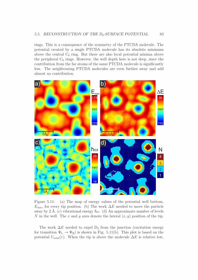
5.5. RECONSTRUCTION OF THE D2-SURFACE POTENTIAL 83
rings. This is a consequence of the symmetry of the PTCDA molecule. Thepotential created by a single PTCDA molecule has its absolute minimumabove the central C6 ring. But there are also local potential minima abovethe peripheral C6 rings. However, the well depth here is not deep, since thecontribution from the far atoms of the same PTCDA molecule is significantlyless. The neighbouring PTCDA molecules are even further away and addalmost no contribution.
Figure 5.11: (a) The map of energy values of the potential well bottom,Emin, for every tip position. (b) The work ∆E needed to move the particleaway by 2 A. (c) vibrational energy ~ω. (d) An approximate number of levelsN in the well. The x and y axes denote the lateral (x, y) position of the tip.
The work ∆E needed to expel D2 from the junction (excitation energyfor transition ΨL → ΨH) is shown in Fig. 5.11(b). This plot is based on thepotential Utotal(r). When the tip is above the molecule ∆E is relative low,

84 CHAPTER 5. TLS SURFACE SCANNING MICROSCOPY
because the D2 molecule is squeezed in the junction in a shallow potential welland can easily move sideways. When the tip is above the intermolecular area,the tip pushes D2 into the layer. D2 sits in a deep potential well. Therefore,D2 movement is restricted. The work needed to expel D2 out of the junctionwill be up to 4 times larger than when the tip is above the molecule. Theleast stable positions of D2 are when the tip is above the edge of the PTCDAmolecule.
Figure 5.12: (a) Excitation energy of D2 out of the junction obtained fromthe calculations Fig. 5.11. (b) Excitation energy of D2 out of the junctionobtained from the experiment.
The excitation of D2 out of the junction is due to the D2 oscillations inthe junction. Thijssen [178] and Halbritter [174] associate the escape withthe excitation of the transversal mode of D2 oscillation in the junction whereD2 oscillates perpendicular to the current flow direction [174, 178, 179]. Toestimate vibrational frequencies and the number of levels in the well, weapproximate the potential energy with a 2D harmonic well in (x, y)-planearound the point of Emin. Fig. 5.11(c) and (d) show the vibrational energy~ω and the number of levels in the potential well. The harmonic well is goodonly to estimate the ground state. The vibrational energy varies from 18 to29 meV what is in agreement with 29 meV reported in the literature [179].For tip position above the molecule, there are one or two vibrational states.Between the molecules the number of levels can rise up to 4 for the deepestpotential wells.
The number of the states does not vary significantly for the different com-putational parameters (ra, rt, Da, Dt, aa, at, α). The calculations showreasonable numbers of the states in the well. Comparing with experiment,
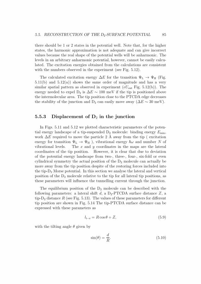
5.5. RECONSTRUCTION OF THE D2-SURFACE POTENTIAL 85
there should be 1 or 2 states in the potential well. Note that, for the higherstates, the harmonic approximation is not adequate and can give incorrectvalues because the real shape of the potential wells will be anharmonic. Thelevels in an arbitrary anharmonic potential, however, cannot be easily calcu-lated. The excitation energies obtained from the calculations are consistentwith the numbers observed in the experiment (see Fig. 5.12).
The calculated excitation energy ∆E for the transition ΨL → ΨH (Fig.5.11(b) and 5.12(a)) shows the same order of magnitude and has a verysimilar spatial pattern as observed in experiment (eUout Fig. 5.12(b)). Theenergy needed to expel D2 is ∆E ∼ 100 meV if the tip is positioned abovethe intermolecular area. The tip position close to the PTCDA edge decreasesthe stability of the junction and D2 can easily move away (∆E ∼ 30 meV).
5.5.3 Displacement of D2 in the junction
In Figs. 5.11 and 5.12 we plotted characteristic parameters of the poten-tial energy landscape of a tip-suspended D2 molecule: binding energy Emin,work ∆E required to move the particle 2 A away from the tip ( excitationenergy for transition ΨL → ΨH ), vibrational energy ~ω and number N ofvibrational levels. The x and y coordinates in the maps are the lateralcoordinates of the tip position. However, it is clear that due to deviationof the potential energy landscape from two-, three-, four-, six-fold or evencylindrical symmetry the actual position of the D2 molecule can actually bemore away from the tip position despite of the restoring forces included intothe tip-D2 Morse potential. In this section we analyse the lateral and verticalposition of the D2 molecule relative to the tip for all lateral tip positions, asthese parameters will influence the tunnelling current through the junction.
The equilibrium position of the D2 molecule can be described with thefollowing parameters: a lateral shift d, a D2-PTCDA surface distance Z, atip-D2 distance R (see Fig. 5.13). The values of these parameters for differenttip position are shown in Fig. 5.14 The tip-PTCDA surface distance can beexpressed with these parameters as
lt−s = R cos θ + Z, (5.9)
with the tilting angle θ given by
sin(θ) =d
R. (5.10)

86 CHAPTER 5. TLS SURFACE SCANNING MICROSCOPY
Figure 5.13: (a) Schematic picture of unperturbed position D2 on the tip. r0is the position of D2 in the potential field Ut of the tip. (b) D2 displacementon the tip in the vicinity of the surface. R is a position of energy minimumof Utotal. Z is a distance to the surface. d is a lateral shift of Emin from thetip (x, y) position.
The lateral shift d (see Fig. 5.14(b)) shows that the maximum value isobserved for tip positions above the borders of the PTCDA molecules, whereD2 feels the repulsive forces from the atoms mainly from one side, and abovethe atoms and bonds where the repulsion rises faster, according to the Morsepotential.
The direction of the lateral shift of equilibrium position of the D2 moleculewith respect to the tip position is shown in Fig. 5.15(a) with small bluearrows. The figure has clear tile pattern where the tile borders are plottedwith white lines. Arrows on opposite sides of the border point in the oppositedirections. When the tip is above the tile, the force acting on the D2 moleculedirects it to the center of the tile. The positions of the tile edges are in agood agreement with the positions of the intramolecular and intermolecularbonds. The tile vertexes coincide with the positions of the atoms of thePTCDA molecules in the layer. The histogram of D2 position distribution(Fig. 5.15(b)) allows us to come to the same conclusions. This tells thatD2-sensor is sensitive to the hydrogen bonds as was proposed before [142].
However, there are complicated situations when two bonds are locatedclose to each other. In this case we do not see an additional tile betweenthem. There is only one border that is shifted towards the shorter bond.For the two bonds of length 1.9 A and 2.2 A (marked with yellow arrows inFigs. 5.15(a) and 5.16), the tile border is near the bond with the length of1.9 A. The closer two atoms are located the stronger is repulsion. Therefore

5.5. RECONSTRUCTION OF THE D2-SURFACE POTENTIAL 87
Figure 5.14: (a) z-position of the energy minima. (b) Magnitude of lateralshift of the energy minima from the tip position (x, y). (c) Distance betweenthe PTCDA layer and D2 molecule. z, R, D are depicted in Fig. 5.13.
above the shorter bond the repulsion grows faster than above the longerbond. This effect is observable in experiment and in calculations. That iswhy the border is shifted away from the longer bond.
In case of PTCDA/Au(111) for the intermolecular area the edges of thetiles coincide with the hydrogen bonds between the neighbouring molecules.PTCDA molecules form “herringbone” structure that is very close to the[102] plane of the bulk structure of the PTCDA crystal. This shape is dueto the stronger intermolecular interaction than the interaction with the Ausubstrate. Intermolecular interactions are represented by hydrogen bondsbetween the neighbouring PTCDA molecules. For “herringbone” structurethey are shorter than any other intermolecular bonds and distances.

88 CHAPTER 5. TLS SURFACE SCANNING MICROSCOPY
5Å
O b)
7
0
N
O
O
O
O
O
O
O
O
O
O
O O O
5Å
a)
Figure 5.15: (a) Tiled structure of the map. White lines denote the bordersbetween the tiles. Small blue arrows show the directions of the lateral shift ofthe position of Emin. The magnitude of the arrow is shown in proportionalitywith a displacement. The backbone structure (red) of PTCDA is superim-posed over the picture. Hydrogen bonds are plotted with black dotted lines.(b) Histogram of the positions of D2 attached to the STM tip during thescanning. N shows how many times D2 is in a position (x, y).
Figure 5.16: Scheme of PTCDA/Au(111) “herringbone” phase with markeddistances.
The parameter R, the tip-D2 distance, depends on how dense atoms ofPTCDA are under the tip (see Fig. 5.14(c)). If the density of the atoms is

5.5. RECONSTRUCTION OF THE D2-SURFACE POTENTIAL 89
small (as in case of the intermolecular area) then the net force acting on theD2 molecule is also small and the R value varies hardly from its unperturbedvalue r0 = 1.9 A. D2 is pushed by the tip into the PTCDA layer. Above theborders of PTCDA, where d value is large, R value changes only slightly, sinceD2 moves circumferentially around the tip apex and try to keep the same tip-D2 distance. A big change of the value R are observed above the areas withhigh density of the atoms, where the lateral movement is restricted (abovethe molecules, but not above the edge of the molecule). Generally speaking,D2 sits in an imaginary pyramid with base vertexes in surface atoms and topin the atom of the tip apex. D2 turns to be squeezed between a tile formedby atoms from below and the atom of the tip from above. The force actingon D2 moves it downwards and to the center of the pyramid base. The largerthe pyramid base is, the stronger D2 is pushed toward the base and the lessthe R varies. This is very well observed in case of the tiles belong to theintermolecular area.
Figure 5.17: Distribution of the value w(R) derived from tip-surface dis-tance. The structure of intermolecular part of the image is identical to theintermolecular structure of the STHM scan image.
Remarkably, for such configuration the image of the value
w(R) =exp(−R)exp(−r0)
(5.11)
will resemble and coincide with the STHM-like contrast of the intermoleculararea in the STHM experiments (see Fig. 5.17). This quantity shows largevalues of the conductance above the molecules and above some intermolecu-lars tiles. w(R) is normalized to the value of the D2 position r0 and follows

90 CHAPTER 5. TLS SURFACE SCANNING MICROSCOPY
the rule how tip’s LDOS changes with distance. Using for w(R) the samelogic that was described above, we will obtain that the magnitude of w(R) issmall for the large tiles (mark (b) in Fig. 5.17), and large for the small tiles(mark (a) and (c) in Fig. 5.17) and the molecules. Abrupt borders are dueto the strong repulsion from the bonds and large shift of the D2 moleculeto the center of one of the tile. Such w(R) behaviour for the intermolecu-lar area is clearly observed for a wide range of the computation parameters.In case of the intramolecular areas w(R) cannot be clearly linked to theSTHM contrast. The variation of w(R) over the molecule is weak and doesnot show clear profile. The corrugation pattern depends on the parametersof the calculation. The parameter Z also does not show visual picture forthe intermolecular structure in case of the STHM contrast. Unfortunately,the current model cannot give an answer how the intramolecular contrast isformed.
5.5.4 PTCDA/Ag(110)
STHM is capable to image local, noncovalent intermolecular interactions,such as hydrogen bonds, in two-dimensional molecular layers [142]. In theSTHM pattern of the PTCDA/Au(111) layer, a remarkable coincidence isobserved between the lines that connect oxygen atoms on one molecule toadjacent hydrogen atoms on neighbouring molecules and the positions atwhich hydrogen bonds are expected. The proposed in section 5.5.1 modelimply that lines are actually related to the shortest connections betweenatoms of neighbouring molecules. In case of PTCDA/Au(111) the shortestconnections between neighbouring PTCDA molecules coincide,in fact, withthe O−H bonds (see Fig. 5.16). But, in general case, this can be not true.
We want to propose that for STHM experiments with PTCDA/Ag(110)O−H bonds should not be observed. PTCDA/Ag(110) adsorbs flat [28] onAg(110) in the “brickwall” commensurate phase [189] where molecules arefacing each other with anhydride groups. The unit cell contains only onePTCDA molecule. A configuration of this phase is due to the strong interac-tion with substrate. PTCDA molecules are oriented on substrate perpendic-ular to the Au rows and then assemble into islands forming hydrogen bonds(see Fig. 5.18 marked with orange). There are two types of O−H bonds withlengths of 3.3 A and 2.7 A. But the shortest connection is actually H−H thatis 2.3 A (see Fig. 5.18 marked with blue line). According to the proposedmodel, in place of the H−H connection position we should observe a line inthe STHM contrast.
5.6. CONCLUSIONS 91
O
O
O
O
O
O
O
O
O
O
O
O
O
O
O
O
O
O
3.3Å
2.7Å2.3Å
Figure 5.18: Scheme of the PTCDA “brickwall” phase on Ag(110). Hydrogenbonds are marked with orange dotted line. Blue dotted lines are expected inSTHM contrast.
Unfortunately, there is no direct experiments with H2 or D2 to provethe statement. But based on the discussion in chapter 3 the intermolecularcontrast in case of D2 (H2) and in case of Xe should coincide. This hasbeen shown for PTCDA/Au(111), and it is expected to be true also forPTCDA/Ag(110). Fig. 5.19 shows STHM-like contrast of PTCDA/Ag(110)obtained with STM tip decorated with Xe atom. A scan image is recordedin the constant height regime with tunnelling parameters I = 1.0 nA andV = −10 mV. The scan image coincide with a scan shown in Fig. 1(h)-(j)in [80]. In case of Xe three lines are observed between the neighbouringPTCDA molecules. As the model predicts, the bright central line coincideswith the H−H connection. Additional sidelines are not very well observed.
5.6 Conclusions
The experiment has shown that the voltage-dependent conductance spec-tra, recorded with a tip decorated with D2 (H2), depend strongly on the tipposition above the surface. The spectra show spike-like features that denoteexcitation of D2 (H2) out of the junction. Measuring spectra in many pointsover the surface and taking slices at particular bias it is possible to reconstructthe conductance scan images for the same bias. The analyses of these scanshave shown laterally inhomogeneous transformation of the STHM contrastinto the STM contrast. For some positions D2 (H2) is restricted to move andtherefore the STHM contrast survives longer. The possibility to reconstructSTHM images from statically measured spectra rules out dynamic effects,such as friction or stick-slip, in STHM image formation.

92 CHAPTER 5. TLS SURFACE SCANNING MICROSCOPY
5Å
a) b)
Figure 5.19: (a) PTCDA/Ag(110), STHM-like contrast obtained with Xedecorated tip in the constant height regime. (b) PTCDA/Ag(110), STHM-like contrast. Enhanced contrast for better view of intermolecular contraststructure.
The state of the junction depends on the position of the tip and on the biasapplied to the junction. The transition between the states happens when theD2 (H2) is excited out of the junction by an inelastically tunnelling electron.For high bias, the junction is empty and have one state. And it can be oneor two low-bias states where D2 (H2) sits in the junction. The reconstructedconstant height images show that for all states with D2 (H2) in the junction,the STHM contrast is observed. The condition of D2 (H2) does not affectthe STHM contrast.
The TLS concept was applied to the junction states. Junction TLS wasused to probe the surface. Moving the tip in the constant height regimeabove the surface and mapping the energy of the excitation of the D2 (H2)out of the junction we have obtained the information that is related to theadsorption energy of the D2-like molecules. To simulate the process of theD2 excitation out of the junction, a force-field model was introduced. Theexcitation energy obtained in calculations was found to be in a good agree-ment with the experiment results. Furthermore, under the proposed modelthe analysis of the displacement of D2 on the tip shows a correlation betweenthe intermolecular STHM contrast and the D2-tip distance. The model pre-dicts that the lines, observed in the experiment and connect the molecules,are related, actually, to the shortest line segments with endpoints in theatoms of the adjacent molecules. And, in the general case, it is not necessarythat these line segments coincide with the intermolecular bonds what was

5.6. CONCLUSIONS 93
proposed earlier. This force-field model despite its simplicity gives interest-ing and important results that allow us to understand the formation of theSTHM contrast better.

94 CHAPTER 5. TLS SURFACE SCANNING MICROSCOPY
Chapter 6
Summary and Outlook
Direct imaging of the inner structure of molecules has always been thechallenge for the surface science. Scanning probe methods with decorated tipsshow that they are a powerful instrument for surface studies. An applicationof complex probes like a tip with an attached single molecule or a singleatom allows to get an image of the surface with atomic precision. Due tothe new physics involved in the tip surface interaction new details about thesurface properties can be obtained. The decorated STM tips can be sensitiveto the structure of the substrate, what means it could be used to describethe geometrical structure of the molecules and what can be useful for thechemical and physical characterisation of the molecules.
6.1 Main results of the work
In the first part of the thesis it was reported that the individual Xe atomor the single CO or CH4 molecule adsorbed on the STM tip apex create a mi-croscopic single particle sensor that simultaneously performs the function ofan atomic-scale force sensor and a signal transducer, which couples the short-range force acting on the tip to the tunnelling conductance of the junctionExperiments with new gases have shown unambiguously that a single particleplays role for structural contrast formation. Single molecule sensors demon-strate geometrical resolution of the surface similar to the STHM resolutionthat was achieved previously with hydrogen or deuterium. The mechanismof the submolecular geometrical contrast resolution does not depend on thedetails of the sensor particle or its interaction with a tip what points outthat it should be a general physical phenomenon. The single particle sen-
95
96 CHAPTER 6. SUMMARY AND OUTLOOK
sors can be characterized with a sensitivity range, which shows how deep thesensor can probe the surface beneath them. This characteristic is importantbecause it helps to choose the proper sensor to study the particular surface.
In the second part of the thesis, it was reported that the structural con-trast of the surface can be obtained simultaneously in the conductance andthe force channels. The particle decorating the tip simultaneously performsthe function of the atomic-scale force sensor and the transducer which cou-ples the short-range force acting on the tip to the tunnelling conductanceof the junction. The coupling between the force and the conductance wasobserved and discussed. On the basis of the experimental data, two distinctcoupling regimes are identified. In the first regime, the coupling show lineardependence and the force sensor-transducer function can be calibrated quan-titatively. In the second regime, the coupling has an irregular complicatedcharacter, which depends on the shape of the tip.
In the third part of the thesis the voltage-dependent conductance spectrarecorded with the STM tip decorated with D2 have been discussed. Theexperiment performed on the “herringbone” phase of PTCDA/Au(111) hasshown that the STM junction can switch between different states, owing tothe excitation of the D2 molecule out of the junction by inelastically tun-nelling electrons. Due to this property, the STM junction was considered asa TLS that can be used to probe the surface. The variation of the energyneeded to expel D2 from the junction is related to the geometrical structureof the surface and hold the information about the excitation energy of D2
from the surface. The excitation energy calculated using a force-field modelwas found to be in a good agreement with the experiment results. The anal-ysis of the displacement of D2 on the tip have shown a correlation betweenthe STHM contrast of the intermolecular area of the PTCDA layer and thevariation of the D2-tip distance. According to the model, the lines betweenthe molecules are related to the shortest connections between the atoms ofthe adjacent molecules. And, in the general case, this line can not coincidewith the intermolecular bonds as it was proposed earlier.
6.2 Future development
The imaging of the surface with the tip gives the information about theprocesses occur on the surfaces. Such methods will be important for study thechemical reactions on the surfaces and a single molecule chemistry. It makespossible to see how reactions proceed on surfaces and define products by
6.2. FUTURE DEVELOPMENT 97
scanning the surface with the tip. There are some reported examples obtainedwith NC-AFM where the functionalized tip was used to define the structure ofthe unknown molecules [79] or to study the single molecule chemical reaction[190]. In such a case an application of the STM with a functionalized tip cangive solutions of such a kind of the problems with much less effort.
All the main experiments have been performed with PTCDA molecules.The layer of PTCDA has complicated structure that depends on the surface.Experiments with PTCDA have shown that it is possible to use STM tip forchemical characterization of the surface. The numerical calculations for thePTCDA are quite complicated. Nevertheless, simple models of the compli-cated objects give a good result. For further study it is necessary to switch tothe simple objects that are very well investigated and more precise models.Simple objects can be calculated with much less effort and gives more pro-found understanding of the physical phenomena, which plays here the role.A couple of steps were made in this direction. The STM tip decorated withCO and with Xe molecule was used to obtain scans of the layers of xenon andsodium chloride. For these simple objects, an interesting and sophisticatedcontrast corrugation of the image was observed. It was found that the con-trast shape strongly depends on the tip-surface distance. A layer of xenon orsodium chloride can be calculated with the modern tools to get results whichcan make a big contribution of the understanding of the STHM-like geo-metrical contrast formation. This knowledge opens new horizons in surfacescience and gives understanding for the further application of functionalizedtips.

98 CHAPTER 6. SUMMARY AND OUTLOOK
Appendix
Program code
Program code listing of the routine to calculate potential energy for tip-surface system for chapter 5. Code is written for Octave/MATLAB.
1 # Plot the U_total field distribution
# Routine for calculating Morse potential for PTCDA layer and the tip
# Routine for calculation the displacement of the D2 position
# prepare the memory for calculations
6 close all;
clc;
clear all
###################################################################
11 # function description part
###################################################################
function [areax, areay, areaz] = prepare_space(z)
# describe the area of interest for calculation
16 # define the center of area
areaCenterCoord = [0,-8.5];
# define width and length of the area
areaSize = [1,1]*20;
# define starting z-distance above the PTCDA layer
21 areaHborder = [0.1,z];
areaBorderPos = 1/2*[areaSize’,areaSize’]*diag([-1,1])+\
[areaCenterCoord’ , areaCenterCoord’];
# number of grid points
x_points = 101;
26 y_points = 101;
z_points = 101;
listx = linspace(areaBorderPos(1), areaBorderPos(3),x_points);
listy = linspace(areaBorderPos(2), areaBorderPos(4),y_points);
99

100 CHAPTER 6. SUMMARY AND OUTLOOK
31 listz = linspace(areaHborder(1), areaHborder(2),z_points);
[areax, areay, areaz] = meshgrid(listx, listy, listz);
endfunction
# STM tip is implemented as single atom with a charge on it
36 # charge part is not used for calculations
function [charges, qQ] = create_tip(x,y,z)
charges = [x, y, z]; # coordinates of charge [x, y, z]
qQ = [0]; # values of charges in colon (is not used)
endfunction
41
# create layer of PTCDA
# mol_num - order of further neighbour
# Prepare to read the file PTCDA_HB.hin with description of
# the unit cell of PTCDA/Au(111)
46 function [charges, qQ] = create_PTCDA_hb_layer(mol_num)
fid = fopen("PTCDA_HB.hin");
rrline = fgets(fid); rrline = fgets(fid); rrline = fgets(fid);
# load atom position of two molecules of one unit cell from the file
51 for molnum = 1:2,
rrline = fgets(fid); rrline = fgets(fid);
for ii = 1:38,
rrline = fgets(fid);
ns = findstr(’ ’,rrline);
56 for i3 = 6:9,
met(ii+(molnum-1)*38,i3-5) = \
str2num( rrline( [ns(i3)+1 : ns(i3+1)-1] ) );
end;
end;
61 end
# read and load translation vectors
rrline = fgets(fid);rrline = fgets(fid);rrline = fgets(fid);
ns = findstr(’ ’,rrline);
rv = diag(ones(6));
66 ii = 1;
for i3 = 1:2,
rv(ii) = str2num( rrline( [ns(i3)+1 : ns(i3+1)-1] ) );
ii = ii+1;
end
71 rrline = fgets(fid);
ns = findstr(’ ’,rrline);
for i3 = 1:2,
rv(ii) = str2num( rrline( [ns(i3)+1 : ns(i3+1)-1] ) );
ii = ii+1;
76 end;
rrline = fgets(fid);
ns = findstr(’ ’,rrline);
for i3 = 1:2,

6.2. FUTURE DEVELOPMENT 101
rv(ii) = str2num( rrline( [ns(i3)+1 : ns(i3+1)-1] ) );
81 ii = ii+1;
end;
fclose(fid);
shiftVec = [rv(3)-rv(1), rv(4)-rv(2) ; \
rv(5)-rv(1), rv(6)-rv(2) ]’*1;
86 qQNa = [];
chargesNa = [];
cellNum = mol_num;
# create a layer of PTCDA consisted of (2*cellNum+1)*(2*cellNum+1) unit cells
91 for ii = -cellNum:cellNum,
for jj = -cellNum:cellNum,
aaa = [met(:,2:3)+\
[(shiftVec*[ii;jj])(1)*ones(size(met)(1),1), \
(shiftVec*[ii;jj])(2)*ones(size(met)(1),1)], \
96 met(:,4)];
qQNa = [qQNa, met(:,1)’];
chargesNa = [chargesNa; aaa];
end
end
101 qQ = qQNa;
charges = chargesNa;
endfunction
# calculate Pauli repulsion potential and gradient for every point
106 # of the grid for PTCDA layer
function [U, Ex, Ey, Ez] = \
potential_Pauli_artificial(r, chargeRx, chargeRy, chargeRz )
r = r;
D = 1;
111 dist = 3.5;
aa = 2;
# 4.5 coefficient to convert to meV
dd = D*exp(aa*dist) * 4.5;
U = dd.*exp(-aa.*r) ;
116 Ex = -aa .* U .* chargeRx ./r;
Ey = -aa .* U .* chargeRy ./r;
Ez = -aa .* U .* chargeRz ./r;
endfunction
121 # calculate chemical potential and gradient for every
# point of the grid for PTCDA layer
function [U, Ex, Ey, Ez ] = \
potential_chem_artificial(r, chargeRx, chargeRy, chargeRz )
r = r;
126 D = 1;
dist = 3.5;
aa = 1;

102 CHAPTER 6. SUMMARY AND OUTLOOK
# 4.5 coefficient to convert to meV
dd = -2*D*exp(aa*dist) * 4.5;
131 U = dd.*exp(-aa.*r) ;
Ex = -aa .* U .* chargeRx ./r;
Ey = -aa .* U .* chargeRy ./r;
Ez = -aa .* U .* chargeRz ./r;
endfunction
136
# calculate Pauli repulsion potential and gradient for every point
# of the grid for the tip
function [U, Ex, Ey, Ez] = \
potential_Pauli_artificial_tip(r, chargeRx, chargeRy, chargeRz )
141 r = r;
D = 25;
dist = 1.9;
aa = 2;
# 4.5 coefficient to convert to meV
146 dd = D*exp(aa*dist)* 4.5;
U = dd.*exp(-aa.*r) ;
Ex = -aa .* U .* chargeRx ./r;
Ey = -aa .* U .* chargeRy ./r;
Ez = -aa .* U .* chargeRz ./r;
151 endfunction
# calculate chemical potential and gradient for every point
# of the grid for the tip
function [U, Ex, Ey, Ez ] = \
156 potential_chem_artificial_tip(r, chargeRx, chargeRy, chargeRz )
r = r;
D = 25;
dist = 1.9;
aa = 1;
161 # 4.5 coefficient to convert to meV
dd = -2*D*exp(aa*dist)* 4.5;
U = dd.*exp(-aa.*r) ;
Ex = -aa .* U .* chargeRx ./r;
Ey = -aa .* U .* chargeRy ./r;
166 Ez = -aa .* U .* chargeRz ./r;
endfunction
# calculate 1/z values for every point of volume of interest
function [chargeRx, chargeRy, chargeRz ] = \
171 uniform_relation(areaz,qCoord)
chargeRx = - qCoord(1);
chargeRy = - qCoord(2);
chargeRz = areaz - qCoord(3);
endfunction
176
# calculate 1/r, where r = (x,y,z)
6.2. FUTURE DEVELOPMENT 103
function [chargeRx, chargeRy, chargeRz ] = \
spherical_relation(areax, areay, areaz, qCoord)
chargeRx = areax - qCoord(1);
181 chargeRy = areay - qCoord(2);
chargeRz = areaz - qCoord(3);
endfunction
# calculate angular coefficient for the tip field calculation
186 function [out] = getAngleCoeff(areax, areay, areaz, qCoord)
chargeRx = areax - qCoord(1);
chargeRy = areay - qCoord(2);
chargeRz = areaz - qCoord(3);
rs = component2abs(chargeRx, chargeRy, 0);
191 r = component2abs(chargeRx, chargeRy, chargeRz);
# kd - coefficient of variation, shows how stable is the position under the tip
kd = 0.5;
out = (1-kd*(rs./r).^2);
endfunction
196
# calculate potentials and fields created by PTCDA layer
function [U, Ex, Ey, Ez ] = \
potentials2(areax,areay,areaz, chargesPosition, qQValue)
# prepare initial grid
201 U_pauli = zeros([size(areax)]);
U_chem = zeros([size(areax)]);
U_vdw = zeros([size(areax)]);
U_el = zeros([size(areax)]);
Ex = zeros([size(areax)]);
206 Ey = zeros([size(areax)]);
Ez = zeros([size(areax)]);
# fill grid with values
for ii = 1:(size(qQValue)(2))
[chargeRx, chargeRy, chargeRz ] = \
211 spherical_relation(areax, areay, areaz, chargesPosition(ii,:));
r = component2abs(chargeRx, chargeRy, chargeRz);
[U1, Ex1, Ey1, Ez1] = \
potential_Pauli_artificial(r, chargeRx, chargeRy, chargeRz) ;
216 [U2, Ex2, Ey2, Ez2] = \
potential_chem_artificial( r, chargeRx, chargeRy, chargeRz) ;
[U3, Ex3, Ey3, Ez3] = \
potential_vdW( r, chargeRx, chargeRy, chargeRz) ;
221 U_pauli = U_pauli + U1 ;
U_chem = U_chem + U2 ;
U_vdw = U_vdw + U3; # is not used
Ex = Ex + Ex1 + Ex2 + Ex3; # is not used
226 Ey = Ey + Ey1 + Ey2 + Ey3;

104 CHAPTER 6. SUMMARY AND OUTLOOK
Ez = Ez + Ez1 + Ez2 + Ez3;
end
# return values
U.pauli = U_pauli;
231 U.chem = U_chem;
U.vdw = U_vdw ;
endfunction
# calculate potentials and fields created by the tip
236 function [U, Ex, Ey, Ez ] = \
potentialsTip(areax,areay,areaz,chargesPosition,qQValue)
# prepare initial grid
U_pauli = zeros([size(areax)]);
U_chem = zeros([size(areax)]);
241 U_vdw = zeros([size(areax)]);
U_el = zeros([size(areax)]);
Ex = zeros([size(areax)]);
Ey = zeros([size(areax)]);
Ez = zeros([size(areax)]);
246 qQValue = zeros([size(areax)]);
# calculate potential for every point of the grid
for ii = 1:(size(qQValue)(2))
angleCoeff = \
251 getAngleCoeff(areax, areay, areaz, chargesPosition(ii,:));
[chargeRx, chargeRy, chargeRz ] = \
spherical_relation(areax, areay, areaz, chargesPosition(ii,:));
r = component2abs(chargeRx, chargeRy, chargeRz);
256
[U1, Ex1, Ey1, Ez1] = potential_Pauli_artificial_tip(r,0,0,0) ;
[U2, Ex2, Ey2, Ez2] = potential_chem_artificial_tip(r,0,0,0) ;
U_pauli = U_pauli + U1 ;
U_chem = U_chem + U2 ;
261
end
# return values
U.pauli = U_pauli;
U.chem = U_chem;
266 U.vdw = U_vdw ;
U.angCoef = angleCoeff;
endfunction
271 # convert components to distance and to projection
function val = component2abs(x, y, z)
if (z!=0),
val = sqrt(x.*x + y.*y + z.*z);
else,

6.2. FUTURE DEVELOPMENT 105
276 val = sqrt(x.*x + y.*y);
end;
endfunction
# calculate index from coordinate
281 function [m,n] = coord2index(x,y, areax, areay)
[xs,ys, zs] = size(areax);
m = floor((xs-1)/(areax(1,end,1)-areax(1,1,1))*(x-areax(1,1,1))+1);
n = floor((ys-1)/(areay(end,1,1)-areay(1,1,1))*(y-areay(1,1,1))+1);
endfunction
286
# calculate step between grid points in x,y,z directions
function [stepx, stepy, stepz] = getSteps(areax, areay, areaz)
stepx = areax(2,2,2) - areax(2,1,2);
stepy = areay(2,2,2) - areay(1,2,2);
291 stepz = areaz(2,2,2) - areaz(2,2,1);
endfunction
# find energy needed to shift D2 for particular distance
# and coordinate of the point
296 function [Point]=getFringeEnergy2D(x,y,zmap,myXTipPos,\
myYTipPos,radius)
# debug flag
debugflag = 0;
# iteration step in energy
301 energy_step = 0.1;
# initial parameters for
Point.En = NA;
Point.x = myXTipPos;
Point.y = myYTipPos;
306 # get index from point coordination
x_index = floor((myXTipPos-x(1))/(x(end)-x(1))*(length(x)-1)+1);
y_index = floor((myYTipPos-y(1))/(y(end)-y(1))*(length(y)-1)+1);
xmin_index = max ( floor( ( (myXTipPos - radius) - x(1)) \
311 / (x(end)-x(1)) * (length(x)-1) +1),1);
xmax_index = min ( floor( ( (myXTipPos + radius) - x(1)) \
/ (x(end)-x(1)) * (length(x)-1) +1),length(x));
ymin_index = max ( floor( ( (myYTipPos - radius) - y(1)) \
316 / (y(end)-y(1)) * (length(y)-1) +1),1);
ymax_index = min ( floor( ( (myYTipPos + radius) - y(1)) \
/ (y(end)-y(1)) * (length(y)-1) +1),length(y));
z_cur = zmap(ymin_index:ymax_index, xmin_index:xmax_index);
321 Energy_min_near_tip = min(min(z_cur));
[y_energy_min_index, x_energy_min_index] = ind2sub([length(y), \
length(x)], find( zmap == Energy_min_near_tip));
106 CHAPTER 6. SUMMARY AND OUTLOOK
# esli eto real min it will not move
326 x_area_cur_min = max(x_energy_min_index-3,1);
x_area_cur_max = min(x_energy_min_index+3, length(x));
y_area_cur_min = max(y_energy_min_index-3, 1);
y_area_cur_max = min(y_energy_min_index+3, length(y));
331 z_cur = zmap(y_area_cur_min:y_area_cur_max, \
x_area_cur_min:x_area_cur_max);
# find potential minimum value near for tip position
Energy_min_near_tip_pr = min(min(z_cur));
336 [y_energy_min_index_pr, x_energy_min_index_pr] = \
ind2sub([length(y), length(x)], \
find( zmap == Energy_min_near_tip_pr));
# find potential value for tip position
Energy_under_tip = zmap(y_index, x_index);
341 area_flag = 0*ones(length(y), length(x));
[yy0, xx0] = ind2sub([length(y), length(x)], \
find(zmap < Energy_min_near_tip_pr));
# length(xx0)
346 for ii = 1:length(yy0)
area_flag( yy0(ii), xx0(ii) ) = -1;
end
# Main routine for findings points that are located at certain distance
351 # with minimal work needed to move it there. start from E_min and then
# increasing energy check what points we can reach. Stop if the points is
# at the distance of interest otherwise continue searching.
if ( ((x(x_energy_min_index_pr) - x(x_index))^2 + \
(y(y_energy_min_index_pr) - y(y_index))^2) < radius^2)
356
area_flag(y_energy_min_index_pr, x_energy_min_index_pr) = 1;
flag = 1;
iiE = 0;
361 while(flag)
flag = 0;
iiE = iiE+1;
energy_next_1 = Energy_min_near_tip_pr+energy_step*(iiE-1);
energy_next_2 = Energy_min_near_tip_pr+energy_step*iiE;
366 if (energy_next_2<0)
flag = 1;
end
out = zmap;
371 out( out > energy_next_2 ) = NA;
out( out <= energy_next_1 ) = NA;
[yy, xx] = ind2sub([length(y),length(x)], find(!isna(out)));

6.2. FUTURE DEVELOPMENT 107
xx = [xx; xx0];
yy = [yy; yy0];
376 flag2 = 1;
# add points with new, a bit higher, energy to the sequence
while(flag2)
flag2 = 0 ;
# for each point add neighbour points to sequence
381 for ii = 1:length(xx)
area = [];
for ix = -1:1,
for iy = -1:1,
# check if point is not out of range of calculated area
386 if( xx(ii)+ix!=0 &&\
yy(ii)+iy!=0 &&\
xx(ii)+ix!= length(x) + 1 &&\
yy(ii)+iy!= length(y) + 1 \
)
391 area = [area, area_flag(yy(ii)+iy, xx(ii)+ix)];
end
end
end
# for each point in sequence calculate if it is fulfil selection rule
396 if (max(area) == 1)
area_flag( yy(ii), xx(ii) ) = 1;
dx = x(xx(ii)) - x(x_index);
dy = y(yy(ii)) - y(y_index);
point_tip_dist = sqrt(dx*dx + dy*dy);
401 # stop if point is less than critical distance of radius
if (point_tip_dist <radius)
if ii == 1
refr = 2:length(xx);
elseif ii == length(xx)
406 refr = 1:length(xx)-1;
else
refr = [1:(ii-1),(ii+1):length(xx)];
end
xx = xx(refr);
411 yy = yy(refr);
flag2 = 1;
break
end
flag = 0;
416 energy2excite = zmap(yy(ii), xx(ii) )
Point.En = energy2excite;
Point.x = x(xx(ii));
Point.y = y(yy(ii));
break
421 end
end

108 CHAPTER 6. SUMMARY AND OUTLOOK
end
# fill rest of yy loop with 0
426 for ii = 1:length(xx)
area_flag( yy(ii), xx(ii) ) = -1;
end
xx0 = xx;
yy0 = yy;
431
if (debugflag ==1)
figure
surf(area_flag)
xlabel(’x’);
436 end
end
else
energy2excite = 0;
441 end
endfunction
###################################################################
446 # Function main()
###################################################################
function main(Param)
# preparation procedures
451
# set current position of the tip
tipHightPosition = Param.h;
tipx = Param.x;
tipy = Param.y;
456
# prepare global values that should be calculated once
ifsave = 0; # flag if we need to save value
cutoff = 0.1; # cutoff in z distance to reduce calculating area
global U; # energy potential value
461 global Ex; # energy potential gradient value
global Ey;
global Ez;
global chargesPosition; # position of atoms of PCTDA
global qQValue; # charge values of atoms of PTCDA
466
# allocate volume of interest and create grid for it
[areax, areay, areaz] = prepare_space(tipHightPosition-cutoff);
[stepx, stepy, stepz] = getSteps(areax, areay, areaz);
[xN, yN, zN] = size(areax);
471 zmin = areaz(1);

6.2. FUTURE DEVELOPMENT 109
zmax = areaz(end);
# reload unchanged parameters instead of calculate them again
if(size(U)(2)==0)
476 # create PTCDA layer and buld potential distribution for it
[chargesPosition, qQValue] = create_PTCDA_hb_layer(2);
[U, Ex, Ey, Ez] = \
potentials2(areax, areay, areaz, chargesPosition, qQValue);
end
481
# preview the molecule
if(1)
figure;
plot(chargesPosition(:,1), chargesPosition(:,2),’o’)
486 hold on;
title("PTCDA sketch");
axis equal;
end
491 # calculate potential for tip
# create tip
[chargesPosition1, qQValue1] = \
create_tip(tipx, tipy, tipHightPosition);
496 # calculate potential energy created by tip
[U1, Ex1, Ey1, Ez1] = \
potentialsTip(areax, areay, \
areaz, chargesPosition1, qQValue1);
501 # calculate total potential energy
amplCoef = 1;
amplCoefSurf = 1;
UoiSurf = (U.pauli + U.chem) * amplCoefSurf;
UoiTip = ( U1.pauli + U1.chem).*U1.angCoef*amplCoef;
506 Uoi = UoiTip + UoiSurf;
# preview slices across molecule at certain x or y position
if(1)
# slice positions
511 xslice = [0]; #[tipx];
yslice = [0]; #[tipy];
zslice = []; # no slice at z
# plot picture
figure;
516 h = slice(areax, areay, areaz, Uoi, xslice, yslice, zslice);
colorbar;
set(h, ’EdgeColor’, ’none’)
title(’Energy field’)
if(1) # preview molecule position

110 CHAPTER 6. SUMMARY AND OUTLOOK
521 hold on;
figure;
plot3(chargesPosition1(:,1), chargesPosition1(:,2),’o’)
title("PTCDA slice");
end
526 end
# preview approach curves at certain x,y position of interest
# this part is needed to monitor Morse potential for different point.
if (1)
531 figure;
hold on;
# point 1 # C6 ring center coordinate
poixV = 9.7;
poiyV = 6.1;
536 [m,n] = coord2index(poixV, poiyV, areax, areay);
poiz = [1:zN];
z_coord = areaz(1,1,poiz)(:);
u_value1 = (Uoi)(n, m, poiz)(:);
u_value1(u_value1 >1) =NA; # cut value for better view
541 plot(z_coord, u_value1, ’bo-’);
# point 2 # C atom coordinate
poixV = 10.6;
poiyV = 5;
[m,n] = coord2index(poixV, poiyV, areax, areay);
546 poiz = [1:zN];
z_coord = areaz(1,1,poiz)(:);
u_value1 = (Uoi)(n, m, poiz)(:);
u_value1(u_value1 >1) = NA;
plot(z_coord, u_value1, ’ro-’);
551 # surface below the tip
u_valueSurf = (UoiSurf)(tipyindex, tipxindex, poiz)(:);
u_valueSurf(u_valueSurf >1) =NA;
plot(z_coord, u_valueSurf, ’k.-’);
# tip + surface below tip
556 u_value1 = (Uoi)(tipyindex, tipxindex, poiz)(:);
u_value1(u_value1 >1) =NA;
plot(z_coord, u_value1, ’go-’);
# additional info for
xlabel("z, angstrem");
561 ylabel("U, meV");
title("void(blue), atom(red), tip-surf(green)");
if (ifsave ==1)
print(’-dsvg’, ’-r300’, ’-color’, \
[’Morse_under_tip’,’TH_’,num2str(tipHightPosition*10),\
566 ’_xTip_’, num2str(tipx*10+100),\
’_yTip_’, num2str(tipy*10+100)]);
close;
end

6.2. FUTURE DEVELOPMENT 111
end
571
# preview slice at certain hight (distOfInt)
if (0)
# for distOfInt = [0.5:0.5:3];#(tipHightPosition-cutoff)],
# for distOfInt = [0.5:0.2:4],
576 Energy = min(min(min(Uoi)));
disp(["Energy: ", num2str(Energy)])
[y, x, z] = ind2sub([xN, yN, zN], find( Uoi == Energy));
figure;
distOfInt = 1.6;
581 poiz = floor((zN-1)/(zmax-zmin)*(distOfInt - zmin) + 1);
out = reshape(Uoi(:,:,poiz),xN,yN);
pcolor(areax(1,:,1)(:), areay(:,1,1)(:) , out);
xlabel("x, angstrem");
ylabel("y, angstrem");
586 colorbar;
title( [’slice_TH_’,\
num2str(tipHightPosition*1),\
’_xTip_’, \
num2str(tipx*1),\
591 ’_yTip_’, \
num2str(tipy*1),\
’_zEnergy_’,\
num2str(distOfInt*1),\
’_Energy_’, \
596 num2str(Energy)])
shading flat;
# save result
if (ifsave == 1)
print(’-dsvg’, ’-r300’, ’-color’, \
601 [’bw_map_TH_’,\
num2str(tipHightPosition*10),\
’_xTip_’, \
num2str(tipx*10+100),\
’_yTip_’, \
606 num2str(tipy*10+100),\
’_zEnergy_’,\
num2str(distOfInt*10),\
’_Energy_’, \
num2str(Energy),\
611 ’.svg’]);
close;
end
# preview results
if(1)
616 [PX,PY] = gradient( out, stepx, stepy) ;
figure;
quiver(areax(1,:,1)(:),areay(:,1,1)(:),PX(:,:,1),PY(:,:,1));

112 CHAPTER 6. SUMMARY AND OUTLOOK
axis equal;
hold on;
621 title(’3D vectors model’)
xlabel("x, angstrem");
ylabel("y, angstrem");
end
# preview molecule or point of interest
626 if(1)
hold on;
plot(chargesPosition(:,1), chargesPosition(:,2),’g.’)
end
631 px = polyfit(areax(1,(x-2):(x+2),1)(:), \
Uoi(y,(x-2):(x+2),z)(:),2);
py = polyfit(areay((y-2):(y+2),1,1)(:), \
Uoi((y-2):(y+2),x,z)(:),2);
end
636
# preview vector map of lateral shift of D2
if(1)
[PX,PY,PZ] = gradient(Uoi,stepx,stepy,stepz) ;
for distOfInt = [0.5:0.5:1.5];
641 poiz = floor((zN-1)/(zmax-zmin)*(distOfInt - zmin) + 1);
out = reshape(Uoi(:,:,poiz),xN,yN);
figure;
quiver(areax(1,:,1)(:), areay(:,1,1)(:), \
PX(:,:,poiz), PY(:,:,poiz));
646 axis equal;
hold on;
title( [’3D vectors map: XY vec, Energy_’, \
num2str(distOfInt*10) ]);
xlabel("x, angstrem");
651 ylabel("y, angstrem");
# take map values at distance of poiz
PXmat = PX(:,:,poiz);
PX = PX(:,:,poiz);
dyPX = sign(PX(:,1:end-1,1))-sign(PX(:,2:end,1));
656 dyPX = abs([dyPX, dyPX(:,end,1)]);
PX = PX’;
dxPX = sign(PX(:,1:end-1,1))-sign(PX(:,2:end,1));
dxPX = abs([dxPX, dxPX(:,end,1)]);
PX = PX’;
661
figure;
surf(areax(1,:,1)(:), areay(:,1,1)(:), sqrt(dxPX.^2+dyPX.^2) );
shading flat;
axis equal;
666 colorbar;
title([’dPX, Energy_’, num2str(distOfInt*10) ] );

6.2. FUTURE DEVELOPMENT 113
xlabel("x, angstrem");
ylabel("y, angstrem");
671 figure;
surf(areax(1,:,1)(:), areay(:,1,1)(:), PZ(:,:,poiz));
shading flat;
axis equal;
colorbar;
676 title([’3D vector model: Z vector value, Energy_’, \
num2str(distOfInt*10)]);
xlabel("x, angstrem");
ylabel("y, angstrem");
end
681 end
# find work needed to move D2 away from the tip
if (1)
# for distOfInt = [1.5:0.3:(tipHightPosition-cutoff)],
686 # for distOfInt = [1.5:0.3:3.5],
Energy = min(min(min(Uoi)));
[y, x, z] = ind2sub([xN, yN, zN], find( Uoi == Energy));
distOfInt = areaz(1,1,z)(:) ;
[tipxindex, tipyindex] = coord2index(tipx, tipy, areax, areay);
691 poiz = floor((zN-1)/(zmax-zmin)*(distOfInt - zmin) + 1);
# x, y, z, xxTip (x tip position), yyTip (y tip position), radius
[out] = getFringeEnergy2D(areax(1,:,1), areay(:,1,1), \
Uoi(:,:,z), tipx, tipy, 2);
E_fringe = out.En
696 [xInd, yInd] = coord2index(out.x, out.y, areax, areay)
# find parameters for harmonic potential
px = polyfit(areax(1,(x-2):(x+2),1)(:), \
Uoi(y,(x-2):(x+2),z)(:),2);
pp = polyval(px,areax(1,(x-2):(x+2),1)(:));
701 py = polyfit(areay((y-2):(y+2),1,1)(:), \
Uoi((y-2):(y+2),x,z)(:),2);
pp = polyval(py, areay((y-2):(y+2),1,1)(:) );
# save the results
if (ifsave == 1)
706 print(’-dsvg’, ’-r300’, ’-color’, \
[’line_x_minEnergy_TH_’, num2str(tipHightPosition*10), \
’_x_’, num2str(tipx*10+100),’_y_’,num2str(tipy*10+100),\
’_z_’, num2str(distOfInt*10), ’.svg’]);
close;
711 end
# write to file
if (1)
disp(’writing’)
nameX = ’all_i_want_to do_’;
716 fid = fopen( [’out_TSdist_’, num2str(tipHightPosition*10),\
114 CHAPTER 6. SUMMARY AND OUTLOOK
nameX, ’.txt’ ] ,’a+’);
fprintf(fid,\
’#f\t#f\t#f\t#f\t#f\t#f\t#f\t#f\t#f\t#f\t#f\t#f\n’, \
tipx, tipy, tipHightPosition,\
721 areax(1,x,1), areay(y,1,1), areaz(1,1,z),\
areax(1,xInd,1), areay(yInd,1,1), \
Energy, E_fringe, \
px(1), py(1)
);
726 fclose(fid);
end
end
# show 3D picture
731 if (1)
tolerance = 0.2;
Energy = min(min(min(Uoi)))+0*tolerance
out = Uoi;
out( out > (Energy+tolerance) ) = NA;
736 out( out < (Energy-tolerance) ) = NA;
[y, x, z] = ind2sub([xN, yN, zN], find(!isna(out)));
x1 = areax(1,x,1)(:);
y1 = areay(y,1,1)(:);
z1 = areaz(1,1,z)(:);
741 figure;
plot3(x1,y1,z1,’.’);
xlabel("x, angstrem");
ylabel("y, angstrem");
zlabel("z, angstrem");
746 # zlabel("meV")
# colorbar;
title(["points with the energy of ",num2str(Energy),’, TH_’,\
num2str(tipHightPosition*10),’, xTip_’, \
num2str(tipx*10),’, yTip_’, num2str(tipy*10)])
751 Energy = min(min(min(Uoi)))+2*tolerance
out = Uoi;
out( out > (Energy+tolerance) ) = NA;
out( out < (Energy-tolerance) ) = NA;
[y, x, z] = ind2sub([xN, yN, zN], find(!isna(out)));
756 x2 = areax(1,x,1)(:);
y2 = areay(y,1,1)(:);
z2 = areaz(1,1,z)(:);
hold on;
plot3(x2,y2,z2,’.r’);
761 Energy = min(min(min(Uoi)))+4*tolerance
out = Uoi;
out( out > (Energy+tolerance) ) = NA;
out( out < (Energy-tolerance) ) = NA;

6.2. FUTURE DEVELOPMENT 115
766 [y, x, z] = ind2sub([xN, yN, zN], find(!isna(out)));
x3 = areax(1,x,1)(:);
y3 = areay(y,1,1)(:);
z3 = areaz(1,1,z)(:);
hold on;
771 plot3(x3,y3,z3,’.y’);
set(gcf,’Color’,[0.6,0.6,0.6])
# set(gca,’CameraPosition’,20*[sin(angle) 0 cos(angle) ]);
# preview molecule or point of interest
if(1)
776 hold on;
#figure;
ii = 4;
atom_in_PTCDA = 38; # 30 for core ; 38 for whole
plot3(chargesPosition(\
781 (atom_in_PTCDA*ii+1):(atom_in_PTCDA*(ii+1)),1), \
chargesPosition(\
(atom_in_PTCDA*ii+1):(atom_in_PTCDA*(ii+1)),2),’ok’)
hold on;
786 ii = 0;
plot3(chargesPosition(\
(atom_in_PTCDA*ii+1):(atom_in_PTCDA*(ii+1)),1),\
chargesPosition(\
(atom_in_PTCDA*ii+1):(atom_in_PTCDA*(ii+1)),2),’ok’)
791
Energy = min(min(min(Uoi)));
[y, x, z] = ind2sub([xN, yN, zN], find( Uoi == Energy));
distOfInt = areaz(1,1,z)(:);
poiz = z;
796 out = reshape(Uoi(:,:,poiz),xN,yN);
pcolor(areax(1,:,1)(:), areay(:,1,1)(:) , out);
shading flat;
end
view(240, 30);
801 if(ifsave == 5)
print(’-dsvg’, ’-r300’, ’-color’, \
[’3D_’,\
’TH_’,\
num2str(tipHightPosition*10),\
806 ’_xTip_’, \
num2str(tipx*10+100),\
’_yTip_’, \
num2str(tipy*10+100)]);
close;
811 end
name = [’TH_’,num2str(tipHightPosition*10),’_3D’];
# prepare data to save
toSave.x1 = x1;

116 CHAPTER 6. SUMMARY AND OUTLOOK
toSave.z1 = z1;
816 toSave.y1 = y1;
toSave.x2 = x2;
toSave.z2 = z2;
toSave.y2 = y2;
toSave.x3 = x3;
821 toSave.z3 = z3;
toSave.y3 = y3;
toSave.chargesPosition = chargesPosition;
toSave.areax = areax;
toSave.areay = areay;
826 toSave.out = out;
save name toSave;
close;
end
endfunction
831
###################################################################
# program starts here
###################################################################
836 # x and y steps of grid for tip position
mystep = (20/127);
# h - z-position of the tip;
# x,y - x and y position of the tip
[h ,y, x] = meshgrid( [4], -5:mystep:12, -11:mystep:6 );
841
allval = length(x(:));
for ii = 1:length(x(:))
Param(ii).x = x(ii);
Param(ii).y = y(ii);
846 Param(ii).h = h(ii);
end
# global parameters needed to calculate once to save total
# computational time
851 global U;
global Ex;
global Ey;
global Ez;
global chargesPosition;
856 global qQValue;
for tt = 1:allval
clear -x tt Param allval U Ex Ey Ez chargesPosition qQValue;
main(Param(tt));
861 end

6.2. FUTURE DEVELOPMENT 117
The description of the unit cell of PTCDA on Au(111).
% Description of the herring bone structure of PTCDA layer
% structure of the string is the next:
% name #num - atom_descroption atom_position - partial_charge_value x y z
4 %
% mol 1
atom 1 - C 0.004196167 0.1528866 -3.744266 0.01138122
atom 2 - C -0.1479287 -1.209324 -3.550244 0.005194386
atom 3 - C -0.108273 1.021363 -2.635129 0.01064787
9 atom 4 - C 0.01191139 0.5325196 -1.34359 0.004555251
atom 5 - C -0.03022575 -0.8769351 -1.12241 0.00149474
atom 6 - C 0.0245142 -1.744455 -2.232792 0.0008782791
atom 7 - C -0.1479268 -3.152233 -2.032282 -0.003795298
atom 8 - C 0.01191235 -1.432525 0.1916723 -0.0007755269
14 atom 9 - C -0.1082726 -2.80397 0.3535403 -0.004852661
atom 10 - C 0.004196405 -3.67005 -0.7574658 -0.006796176
atom 11 - C -0.1479297 3.152227 2.032275 -0.004544073
atom 12 - C 0.02451372 1.744451 2.232796 9.880461e-006
atom 13 - C 0.004193544 3.670039 0.7574549 -0.006938186
19 atom 14 - C -0.1082716 2.803954 -0.3535442 -0.003388885
atom 15 - C 0.01190948 1.432511 -0.1916624 0.0007271195
atom 16 - C -0.0302248 0.8769233 1.122421 0.0008460354
atom 17 - C 0.01191139 -0.5325347 1.343607 0.001470514
atom 18 - C -0.1479259 1.209327 3.550254 0.003406957 3
24 atom 19 - C 0.004196167 -0.1528943 3.74429 0.005388714
atom 20 - C -0.1082721 -1.021377 2.63516 0.003597346
atom 21 - H 0.1296895 0.5699118 -4.759921 0.01639607
atom 22 - H 0.1222507 2.111245 -2.799161 0.01430543
atom 23 - H 0.1222504 3.226784 -1.371374 -0.003759135
29 atom 24 - H 0.129689 4.756413 0.5985163 -0.01149259
atom 25 - H 0.1222502 -2.111263 2.799208 0.003753818
atom 26 - H 0.1296894 -0.569921 4.759953 0.008180749
atom 27 - H 0.1222503 -3.226808 1.371366 -0.006442073
atom 28 - H 0.1296895 -4.75643 -0.5985366 -0.01053608
34 atom 29 - C 0.4089208 4.031771 3.22193 -0.00711445
atom 30 - C 0.4089148 2.150876 4.691456 0.005151376
atom 31 - O -0.3057137 5.240309 3.273805 -0.01400339
atom 32 - O -0.3057232 1.90885 5.87667 0.01171442
atom 33 - O -0.2243776 3.512439 4.495692 -0.001118116
39 atom 34 - C 0.4089155 -2.150849 -4.691467 0.002481526
atom 35 - C 0.4089139 -4.031764 -3.221941 -0.005188323
atom 36 - O -0.3057203 -1.908796 -5.876687 0.003530481
atom 37 - O -0.3057222 -5.240334 -3.273822 -0.008757038
atom 38 - O -0.2243714 -3.512417 -4.495708 -0.002410372
44 % endmol 1
% mol 2
atom 1 - C 0.004196167 13.27003 5.392527 0.01138122
atom 2 - C -0.1479287 12.75223 4.117719 0.005194387
atom 3 - C -0.108273 12.40394 6.503535 0.01064787

118 CHAPTER 6. SUMMARY AND OUTLOOK
49 atom 4 - C 0.01191139 11.03251 6.341655 0.00455525
atom 5 - C -0.03022575 10.47692 5.027581 0.001494739
atom 6 - C 0.0245142 11.34445 3.917206 0.0008782792
atom 7 - C -0.1479268 10.80932 2.59975 -0.003795298
atom 8 - C 0.01191235 9.067465 4.8064 -0.0007755269
54 atom 9 - C -0.1082726 8.578621 3.514849 -0.004852662
atom 10 - C 0.004196405 9.4471 2.405717 -0.006796175
atom 11 - C -0.1479297 8.390684 9.700246 -0.004544074
atom 12 - C 0.02451372 7.855551 8.382794 9.880516e-006
atom 13 - C 0.004193544 9.752909 9.89427 -0.006938186
59 atom 14 - C -0.1082716 10.62138 8.785129 -0.003388885
atom 15 - C 0.01190948 10.13252 7.493592 0.0007271195
atom 16 - C -0.0302248 8.723068 7.272421 0.0008460354
atom 17 - C 0.01191139 8.167473 5.958335 0.001470514
atom 18 - C -0.1479259 6.447769 8.18229 0.003406957
64 atom 19 - C 0.004196167 5.929943 6.907474 0.005388714
atom 20 - C -0.1082721 6.796023 5.79646 0.003597346
atom 21 - H 0.1296895 14.3564 5.55145 0.01639607
atom 22 - H 0.1222507 12.82677 7.52136 0.01430543
atom 23 - H 0.1222504 11.71127 8.949176 -0.003759135
69 atom 24 - H 0.129689 10.16994 10.90992 -0.01149259
atom 25 - H 0.1222502 6.373182 4.778641 0.003753817
atom 26 - H 0.1296894 4.843561 6.748544 0.008180749
atom 27 - H 0.1222503 7.488733 3.350804 -0.006442073
atom 28 - H 0.1296895 9.030073 1.390055 -0.01053608
74 atom 29 - C 0.4089208 7.449148 10.84146 -0.007114451
atom 30 - C 0.4089148 5.568247 9.371955 0.005151376
atom 31 - O -0.3057137 7.691187 12.02665 -0.01400339
atom 32 - O -0.3057232 4.359686 9.423846 0.01171442
atom 33 - O -0.2243776 6.087586 10.64571 -0.001118116
79 atom 34 - C 0.4089155 13.63177 2.928071 0.002481526
atom 35 - C 0.4089139 11.75086 1.458541 -0.005188322
atom 36 - O -0.3057203 14.84034 2.8762 0.003530481
atom 37 - O -0.3057222 11.50882 0.2733212 -0.008757038
atom 38 - O -0.2243714 13.11244 1.654311 -0.002410372
84 % endmol 2
% Translation vector description
0 1.90885 5.87667
1 21.10885 5.87667
2 1.908851 18.17667

Bibliography
[1] C. W. Tang and S. A. Van Slyke. Organic electroluminescent diodes.Applied Physics Letters, 51:913, 1987.
[2] J. Blochwitz, T. Fritz, M. Pfeiffer, K. Leo, D. M. Alloway, P. A. Lee,and N. R. Armstrong. Interface electronic structure of organic semicon-ductors with controlled doping levels. Organic Electronics, 2(2):97–104,2001.
[3] K. Walzer, B. Maennig, M. Pfeiffer, K. Leo, et al. Highly efficientorganic devices based on electrically doped transport layers. ChemicalReviews-Columbus, 107(4):1233–1271, 2007.
[4] Norbert Koch. Organic electronic devices and their functional inter-faces. ChemPhysChem, 8(10):1438–1455, 2007.
[5] Klaus Mullen and Ullrich Scherf. Organic light emitting devices. WileyOnline Library, 2006.
[6] J. H. Burroughes, D. D. C. Bradley, A. R. Brown, R. N. Marks,K. Mackay, R. H. Friend, P. L. Burns, and A. B. Holmes. Light-emittingdiodes based on conjugated polymers. nature, 347(6293):539–541, 1990.
[7] Henning Sirringhaus, Nir Tessler, and Richard H. Friend. Inte-grated optoelectronic devices based on conjugated polymers. Science,280(5370):1741–1744, 1998.
[8] R. H. Friend, R. W. Gymer, A. B. Holmes, J. H. Burroughes, R.N. Marks, C. D. D. C. Taliani, D. D. C. Bradley, D. A. Dos Santos,J. L. Bredas, M. Logdlund, et al. Electroluminescence in conjugatedpolymers. Nature, 397(6715):121–128, 1999.
[9] Peter Peumans, Soichi Uchida, and Stephen R Forrest. Efficient bulkheterojunction photovoltaic cells using small-molecular-weight organicthin films. Nature, 425(6954):158–162, 2003.
119

120 BIBLIOGRAPHY
[10] Barry P. Rand, Jan Genoe, Paul Heremans, and Jef Poortmans. Solarcells utilizing small molecular weight organic semiconductors. Progressin Photovoltaics: Research and Applications, 15(8):659–676, 2007.
[11] B. Maennig, J. Drechsel, D. Gebeyehu, P. Simon, F. Kozlowski,A. Werner, Fenghong Li, S. Grundmann, S. Sonntag, M. Koch, et al.Organic pin solar cells. Applied Physics A, 79(1):1–14, 2004.
[12] P. Peumans, V. Bulovic, and S.R. Forrest. Efficient photon harvestingat high optical intensities in ultrathin organic double-heterostructurephotovoltaic diodes. Applied Physics Letters, 76(19):2650–2652, 2000.
[13] Ruth Shinar and Joseph Shinar. Organic electronics in sensors andbiotechnology. McGraw-Hill, Inc., 2009.
[14] Giuseppe Arrabito and Bruno Pignataro. Solution processed micro-and nano-bioarrays for multiplexed biosensing. Analytical chemistry,84(13):5450–5462, 2012.
[15] Ching W. Tang. Two-layer organic photovoltaic cell. Applied PhysicsLetters, 48:183, 1986.
[16] Peter Strohriegl and Juozas V. Grazulevicius. Charge-transportingmolecular glasses. Advanced Materials, 14(20):1439–1452, 2002.
[17] Gilles Horowitz. Organic thin film transistors: From theory to realdevices. J. Mater. Res, 19(7):1946–1962, 2004.
[18] W. Clemens, W. Fix, J. Ficker, A. Knobloch, and A. Ullmann. Frompolymer transistors toward printed electronics. Journal of MaterialsResearch, 19(7):1963–1973, 2004.
[19] Susanne Scheinert and Gernot Paasch. Fabrication and analysis ofpolymer field-effect transistors. physica status solidi (a), 201(6):1263–1301, 2004.
[20] Fabio Cicoira and Clara Santato. Organic light emitting field effecttransistors: advances and perspectives. Advanced Functional Materials,17(17):3421–3434, 2007.
[21] A. Dodabalapur, L. Torsi, and H. E. Katz. Organic transistors: two-dimensional transport and improved electrical characteristics. Science,268(5208):270–271, 1995.
[22] Ananth Dodabalapur, H. E. Katz, L. Torsi, and R. C. Haddon. Organicheterostructure field-effect transistors. Science, 269(5230):1560–1562,1995.

BIBLIOGRAPHY 121
[23] S. F. Nelson, Y-Y. Lin, D. J. Gundlach, and T. N. Jackson.Temperature-independent transport in high-mobility pentacene tran-sistors. Applied physics letters, 72(15):1854–1856, 1998.
[24] Tommie W. Kelley, Paul F. Baude, Chris Gerlach, David E. Ender,Dawn Muyres, Michael A. Haase, Dennis E. Vogel, and Steven D.Theiss. Recent progress in organic electronics: Materials, devices, andprocesses. Chemistry of Materials, 16(23):4413–4422, 2004.
[25] Ullrich Mitschke and Peter Bauerle. The electroluminescence of organicmaterials. Journal of Materials Chemistry, 10(7):1471–1507, 2000.
[26] Terje A. Skotheim and John R. Reynolds. Handbook of conductingpolymers, volume 2. CRC PressI Llc, 2007.
[27] K. Oura. Surface Science: An Introduction. Advanced Texts in Physics.Springer, 2003.
[28] Y. Zou, L. Kilian, A. Scholl, Th. Schmidt, R. Fink, and E. Umbach.Chemical bonding of PTCDA on ag surfaces and the formation ofinterface states. Surface Science, 600(6):1240–1251, 2006.
[29] Takashi Kataoka, Hirohiko Fukagawa, Shunsuke Hosoumi, KohjiroNebashi, Kazuyuki Sakamoto, and Nobuo Ueno. Observation of atemperature-dependent transition of a copper-phthalocyanine thin filmadsorbed on hopg. Chemical Physics Letters, 451(1):43–47, 2008.
[30] Andreas Langner, Annegret Hauschild, Sonja Fahrenholz, and MoritzSokolowski. Structural properties of tetracene films on ag (111) inves-tigated by spa-leed and tpd. Surface science, 574(2):153–165, 2005.
[31] C. Stadler, S. Hansen, F. Pollinger, C. Kumpf, E. Umbach, T.-L. Lee,and J. Zegenhagen. Structural investigation of the adsorption of snpcon ag (111) using normal-incidence x-ray standing waves. PhysicalReview B, 74(3):035404, 2006.
[32] V. Podzorov, E. Menard, A. Borissov, V. Kiryukhin, J. A. Rogers, andM. E. Gershenson. Intrinsic charge transport on the surface of organicsemiconductors. Physical review letters, 93(8):086602, 2004.
[33] V. Podzorov, E. Menard, J. A. Rogers, and M. E. Gershenson. Halleffect in the accumulation layers on the surface of organic semiconduc-tors. Physical review letters, 95(22):226601, 2005.
[34] Alessandro Troisi and Giorgio Orlandi. Charge-transport regime ofcrystalline organic semiconductors: Diffusion limited by thermal off-

122 BIBLIOGRAPHY
diagonal electronic disorder. Physical review letters, 96(8):086601,2006.
[35] Alessandro Troisi and Giorgio Orlandi. Dynamics of the intermoleculartransfer integral in crystalline organic semiconductors. The Journal ofPhysical Chemistry A, 110(11):4065–4070, 2006.
[36] Alessandro Troisi. Prediction of the absolute charge mobility ofmolecular semiconductors: the case of rubrene. Advanced Materials,19(15):2000–2004, 2007.
[37] H. A. v. Laarhoven, Cees F. J. Flipse, Mattijs Koeberg, Mischa Bonn,Euan Hendry, G Orlandi, OD Jurchescu, TTM Palstra, and Alessan-dro Troisi. On the mechanism of charge transport in pentacene. TheJournal of chemical physics, 129:044704, 2008.
[38] J. B. Pendry. Off-diagonal disorder and 1d localisation. Journal ofPhysics C: Solid State Physics, 15(28):5773, 1982.
[39] David P. McMahon and Alessandro Troisi. Organic semiconduc-tors: impact of disorder at different timescales. ChemPhysChem,11(10):2067–2074, 2010.
[40] F.-J. Meyer Zu Heringdorf, M. C. Reuter, and R. M. Tromp. Thenucleation of pentacene thin films. Applied Physics A, 78(6):787–791,2004.
[41] Frank-J. Meyer Zu Heringdorf, M. C. Reuter, and R. M. Tromp.Growth dynamics of pentacene thin films. Nature, 412(6846):517–520,2001.
[42] E. Bauer, M. Mundschau, W. Swiech, and W. Telieps. Surface studiesby low-energy electron microscopy (leem) and conventional uv pho-toemission electron microscopy (peem). Ultramicroscopy, 31(1):49–57,1989.
[43] E. Bauer, Y. Wei, T. Muller, A. Pavlovska, and I. S. T. Tsong. Reactivecrystal growth in two dimensions: Silicon nitride on si (111). PhysicalReview B, 51(24):17891, 1995.
[44] A. Hanisch-Blicharski, A. Janzen, B. Krenzer, S. Wall, F. Klasing,A. Kalus, T Frigge, M Kammler, and M Horn-von Hoegen. Ultra-fast electron diffraction at surfaces: From nanoscale heat transport todriven phase transitions. Ultramicroscopy, 2012.

BIBLIOGRAPHY 123
[45] P. Babelon, A. S. Dequiedt, H. Mostefa-Sba, S. Bourgeois, P. Sibillot,and M. Sacilotti. Sem and xps studies of titanium dioxide thin filmsgrown by mocvd. Thin Solid Films, 322(1):63–67, 1998.
[46] Diana Mardare, M. Tasca, M. Delibas, and G. I. Rusu. On the struc-tural properties and optical transmittance of tio¡ sub¿ 2¡/sub¿ rf sput-tered thin films. Applied Surface Science, 156(1):200–206, 2000.
[47] Christoph Boettcher, Boris Schade, and Juergen-Hinrich Fuhrhop.Comparative cryo-electron microscopy of noncovalent n-dodecanoyl-(d-and l-) serine assemblies in vitreous toluene and water. Langmuir,17(3):873–877, 2001.
[48] Jeffrey D. Hartgerink, Elia Beniash, and Samuel I. Stupp. Self-assembly and mineralization of peptide-amphiphile nanofibers. Science,294(5547):1684–1688, 2001.
[49] N. Mori, T. Oikawa, T. Katoh, J. Miyahara, and Y. Harada. Applica-tion of the “imaging plate” to tem image recording. Ultramicroscopy,25(3):195–201, 1988.
[50] I. Petrov, P. B. Barna, Lars Hultman, and J. E. Greene. Microstruc-tural evolution during film growth. Journal of Vacuum Science & Tech-nology A: Vacuum, Surfaces, and Films, 21(5):S117–S128, 2003.
[51] Rolf Erni, Marta D. Rossell, Christian Kisielowski, and Ulrich Dahmen.Atomic-resolution imaging with a sub-50-pm electron probe. Phys. Rev.Lett., 102:096101, Mar 2009.
[52] G. Binnig, C. F. Quate, and Ch. Gerber. Atomic force microscope.Phys. Rev. Lett., 56:930–933, Mar 1986.
[53] Paul G. Piva, Gino A. DiLabio, Jason L. Pitters, Janik Zikovsky, Moh’dRezeq, Stanislav Dogel, Werner A. Hofer, and Robert A. Wolkow. Fieldregulation of single-molecule conductivity by a charged surface atom.Nature, 435(7042):658–661, 2005.
[54] X. D. Cui, A. Primak, X. Zarate, J. Tomfohr, O. F. Sankey, A.L. Moore, T. A. Moore, D. Gust, Gari Harris, and S. M. Lindsay.Reproducible measurement of single-molecule conductivity. Science,294(5542):571–574, 2001.
[55] B. D. Terris, J. E. Stern, D. Rugar, and H. J. Mamin. Contact electri-fication using force microscopy. Physical Review Letters, 63(24):2669–2672, 1989.

124 BIBLIOGRAPHY
[56] J. E. Stern, B. D. Terris, H. J. Mamin, and D. Rugar. Deposition andimaging of localized charge on insulator surfaces using a force micro-scope. Applied physics letters, 53(26):2717–2719, 1988.
[57] Fabian Mohn, Leo Gross, Nikolaj Moll, and Gerhard Meyer. Imagingthe charge distribution within a single molecule. Nature nanotechnol-ogy, 7(4):227–231, 2012.
[58] D. Rugar, H. J. Mamin, P. Guethner, S. E. Lambert, J. E. Stern, I. Mc-Fadyen, and T. Yogi. Magnetic force microscopy: General principlesand application to longitudinal recording media. Journal of AppliedPhysics, 68(3):1169–1183, 1990.
[59] Y. Martin and H. Kumar Wickramasinghe. Magnetic imaging by“force microscopy” with 1000 a resolution. Applied Physics Letters,50(20):1455–1457, 1987.
[60] C. Mathew Mate, Gary M. McClelland, Ragnar Erlandsson, andShirley Chiang. Atomic-scale friction of a tungsten tip on a graphitesurface. In Scanning Tunneling Microscopy, pages 226–229. Springer,1993.
[61] Jean-Paul Salvetat, Andrzej J. Kulik, Jean-Marc Bonard, G. Andrew,D. Briggs, Thomas Stockli, Karine Metenier, Sylvie Bonnamy, Fran-cois Beguin, Nancy A Burnham, and Laslo Forro. Elastic modulusof ordered and disordered multiwalled carbon nanotubes. AdvancedMaterials, 11(2):161–165, 1999.
[62] Martin Stolz, Roberto Raiteri, A. U. Daniels, Mark R. VanLanding-ham, Werner Baschong, and Ueli Aebi. Dynamic elastic modulus ofporcine articular cartilage determined at two different levels of tissueorganization by indentation-type atomic force microscopy. BiophysicalJournal, 86(5):3269, 2004.
[63] Stephane Cuenot, Sophie Demoustier-Champagne, and Bernard Nys-ten. Elastic modulus of polypyrrole nanotubes. Physical Review Letters,85(8):1690–1693, 2000.
[64] Joseph A. Stroscio and D. M. Eigler. Atomic and molecular manipula-tion with the scanning tunneling microscope. Science, 254(5036):1319–1326, 1991.
[65] Francesca Moresco, Gerhard Meyer, Karl-Heinz Rieder, Hao Tang,Andre Gourdon, and Christian Joachim. Conformational changes ofsingle molecules induced by scanning tunneling microscopy manipula-

BIBLIOGRAPHY 125
tion: A route to molecular switching. Phys. Rev. Lett., 86:672–675,Jan 2001.
[66] Francesca Moresco. Manipulation of large molecules by low-temperature stm: model systems for molecular electronics. PhysicsReports, 399(4):175–225, 2004.
[67] T. C. Shen, C. Wang, G. C. Abeln, J. R. Tucker, J. W. Lyding, Ph.Avouris, and R. E. Walkup. Atomic-scale desorption through electronicand vibrational excitation mechanisms. Science, 268(5217):1590–1592,1995.
[68] L. Zhang, T. Sakai, N. Sakuma, T. Ono, and K. Nakayama. Nanostruc-tural conductivity and surface-potential study of low-field-emission car-bon films with conductive scanning probe microscopy. Applied PhysicsLetters, 75(22):3527–3529, 1999.
[69] J. M. R. Weaver and David W. Abraham. High resolution atomic forcemicroscopy potentiometry. Journal of Vacuum Science & TechnologyB: Microelectronics and Nanometer Structures, 9(3):1559–1561, 1991.
[70] U. Hartmann. Magnetic force microscopy: Some remarks from themicromagnetic point of view. Journal of Applied Physics, 64(3):1561–1564, 1988.
[71] S. R. Higgins and R. J. Hamers. Morphology and dissolution processesof metal sulfide minerals observed with the electrochemical scanningtunneling microscope. volume 14, pages 1360–1364. AVS, 1996.
[72] M. Nonnenmacher, M. P. O’Boyle, and H. K. Wickramasinghe. Kelvinprobe force microscopy. Applied Physics Letters, 58(25):2921–2923,1991.
[73] R. Wiesendanger and M. Bode. Nano- and atomic-scale magnetismstudied by spin-polarized scanning tunneling microscopy and spec-troscopy. Solid State Communications, 119:341–355, 2001.
[74] E. Betzig, J. K. Trautman, T. D. Harris, J. S. Weiner, and R. L. Koste-lak. Breaking the diffraction barrier: Optical microscopy on a nano-metric scale. Science, 251(5000):1468–1470, 1991.
[75] Eric Betzig and Robert J. Chichester. Single molecules observed bynear-field scanning optical microscopy. Science, 262(5138):1422–1425,1993.

126 BIBLIOGRAPHY
[76] D. M. Lewis, J. E. D. Spencer, and B. O. Field. An introduction toinelastic electron tunneling spectroscopy (iets) and its chemical applica-tions. Spectrochimica Acta Part A: Molecular Spectroscopy, 44(3):247–261, 1988.
[77] Elena Bailo and Volker Deckert. Tip-enhanced raman scattering.Chemical Society Reviews, 37(5):921–930, 2008.
[78] R. Berndt, R. Gaisch, J. K. Gimzewski, B. Reihl, R. R. Schlittler, W.D. Schneider, M Tschudy, et al. Photon emission at molecular resolu-tion induced by a scanning tunneling microscope. Science, 262:1425–1425, 1993.
[79] Leo Gross, Fabian Mohn, Nikolaj Moll, Gerhard Meyer, Rainer Ebel,Wael M. Abdel-Mageed, and Marcel Jaspars. Organic structure deter-mination using atomic-resolution scanning probe microscopy. Naturechemistry, 2(10):821–825, 2010.
[80] R. Temirov, S. Soubatch, O. Neucheva, A. C. Lassise, and F. S. Tautz.A novel method achieving ultra-high geometrical resolution in scanningtunnelling microscopy. New Journal of Physics, 10(5):053012, 2008.
[81] G. Binnig, H. Rohrer, Ch. Gerber, and E. Weibel. Tunneling through acontrollable vacuum gap. Applied Physics Letters, 40(2):178–180, 1982.
[82] Johannes A. A. W. Elemans, Inge De Cat, Hong Xu, and Steven DeFeyter. Two-dimensional chirality at liquid-solid interfaces. Chem. Soc.Rev., 38:722–736, 2009.
[83] Johannes A.A.W. Elemans. A new look at the chemical reaction. Ma-terials Today, 12(7–8):34–38, 2009.
[84] Jurgen P. Rabe and Stefan Buchholz. Direct observation of molecularstructure and dynamics at the interface between a solid wall and anorganic solution by scanning tunneling microscopy. Phys. Rev. Lett.,66:2096–2099, Apr 1991.
[85] P. Kowalczyk. High temperature stm/sts investigations of resonantimage states on au (111). Applied surface science, 253(8):4036–4040,2007.
[86] C.T. Herbschleb, S.C. Bobaru, and J.W.M. Frenken. High-pressure stmstudy of no reduction by co on pt(100). Catalysis Today, 154(1–2):61– 67, 2010. ¡ce:title¿Catalytic Surface Science¡/ce:title¿.
BIBLIOGRAPHY 127
[87] L. Bartels, S. Zophel, G. Meyer, E. Henze, and K.-H. Rieder. Dimerformation and surface alloying: a stm study of lead on cu(211). SurfaceScience, 372(1–3):L261–L265, 1997.
[88] M. Kugler, Ch. Renner, V. Mikheev, G. Batey, and Ø. Fischer. A 3hecooled scanning tunneling microscope in uhv and high fields. PhysicaB: Condensed Matter, 280(1–4):551–552, 2000.
[89] John Bardeen. Tunnelling from a many-particle point of view. Phys.Rev. Letters, 6, 1961.
[90] J. Tersoff and D. R. Hamann. Theory and application for the scanningtunneling microscope. Phys. Rev. Lett., 50:1998–2001, Jun 1983.
[91] J. Tersoff and D. R. Hamann. Theory of the scanning tunneling mi-croscope. Phys. Rev. B, 31:805–813, Jan 1985.
[92] C.J. Chen. Introduction to scanning tunneling microscopy. Monographson the physics and chemistry of materials. Oxford University Press,2008.
[93] Leo Gross, Nikolaj Moll, Fabian Mohn, Alessandro Curioni, GerhardMeyer, Felix Hanke, and Mats Persson. High-resolution molecular or-bital imaging using a p-wave stm tip. Phys. Rev. Lett., 107:086101,Aug 2011.
[94] B. N. J. Persson and A. Baratoff. Inelastic electron tunneling from ametal tip: The contribution from resonant processes. Phys. Rev. Lett.,59:339–342, Jul 1987.
[95] D.M. Lewis, J.E.D. Spencer, and B.O. Field. An introduction to inelas-tic electron tunneling spectroscopy (iets) and its chemical applications.Spectrochimica Acta Part A: Molecular Spectroscopy, 44(3):247–261,1988.
[96] J. Lambe and R. C. Jaklevic. Molecular vibration spectra by inelasticelectron tunneling. Phys. Rev., 165:821–832, Jan 1968.
[97] Chi Chen, Ping Chu, C. A. Bobisch, D. L. Mills, and W. Ho. Viewingthe interior of a single molecule: Vibronically resolved photon imagingat submolecular resolution. Phys. Rev. Lett., 105:217402, Nov 2010.
[98] Paolo Samorı. Scanning probe microscopies beyond imaging. Wiley-VCH, 2006.

128 BIBLIOGRAPHY
[99] Nicolas Lorente and M Persson. Theory of single molecule vibrationalspectroscopy and microscopy. Physical review letters, 85(14):2997–3000, 2000.
[100] B. Bhushan. Handbook of Micro/Nano Tribology, Second Edition. TheMechanics and materials science series. Taylor & Francis, 2010.
[101] Nancy A Burnham, Dawn D Dominguez, Robert L Mowery, andRichard J Colton. Probing the surface forces of monolayer films withan atomic-force microscope. Physical review letters, 64(16):1931–1934,1990.
[102] O. Marti, B. Drake, and P. K. Hansma. Atomic force microscopy ofliquid-covered surfaces: Atomic resolution images. Applied PhysicsLetters, 51(7):484–486, 1987.
[103] B. Drake, C. B. Prater, A. L. Weisenhorn, S. A. C. Gould, T. R. Al-brecht, C. F. Quate, D. S. Cannell, H. G. Hansma, and P. K. Hansma.Imaging crystals, polymers, and processes in water with the atomicforce microscope. Science, 243(4898):1586–1589, 1989.
[104] M. Binggeli, R. Christoph, H.-E. Hintermann, J. Colchero, andO. Marti. Friction force measurements on potential controlled graphitein an electrolytic environment. Nanotechnology, 4(2):59, 1993.
[105] Gerhard Meyer and Nabil M. Amer. Novel optical approach to atomicforce microscopy. Applied Physics Letters, 53(12):1045–1047, 1988.
[106] J. H. Coombs and J. B. Pethica. Properties of vacuum tunneling cur-rents: Anomalous barrier heights. j-IBM-JRD, 30(5):455–459, Septem-ber 1986.
[107] M. D. Kirk, T. R. Albrecht, and C. F. Quate. Low-temperature atomicforce microscopy. Review of scientific instruments, 59(6):833–835, 1988.
[108] Giessibl Franz J. Giessibl, Ch. Gerber, and Gerd Binnig. A low-temperature atomic force/scanning tunneling microscope for ultrahighvacuum. Journal of Vacuum Science & Technology B: Microelectronicsand Nanometer Structures, 9(2):984–988, 1991.
[109] T. R. Albrecht, P. Grutter, D. Rugar, and D. P. E. Smith. Low-temperature force microscope with all-fiber interferometer. Ultrami-croscopy, 42:1638–1646, 1992.
[110] Charlotte Basire and Dimitri A. Ivanov. Evolution of the lamellarstructure during crystallization of a semicrystalline-amorphous poly-

BIBLIOGRAPHY 129
mer blend: time-resolved hot-stage spm study. Physical review letters,85(26):5587–5590, 2000.
[111] Huiwen Liu and Bharat Bhushan. Investigation of nanotribologicalproperties of self-assembled monolayers with alkyl and biphenyl spacerchains. Ultramicroscopy, 91(1):185–202, 2002.
[112] T. R. Albrecht, P. Grutter, D. Horne, and D. Rugar. Frequency modu-lation detection using high-q cantilevers for enhanced force microscopesensitivity. Journal of Applied Physics, 69(2):668–673, 1991.
[113] John E. Sader and Suzanne P. Jarvis. Accurate formulas for interactionforce and energy in frequency modulation force spectroscopy. AppliedPhysics Letters, 84(10):1801, 2004.
[114] Franz J. Giessibl. Advances in atomic force microscopy. Rev. Mod.Phys., 75:949–983, Jul 2003.
[115] Franz J. Giessibl. High-speed force sensor for force microscopy andprofilometry utilizing a quartz tuning fork. Applied Physics Letters,73(26):3956–3958, 1998.
[116] F. J. Giessibl. Principles and Applications of the qPlus Sensor, page121. 2009.
[117] John E. Sader and Yoshiaki Sugimoto. Accurate formula for conversionof tunneling current in dynamic atomic force spectroscopy. AppliedPhysics Letters, 97(4):043502, 2010.
[118] C. Weiss, C. Wagner, C. Kleimann, M. Rohlfing, F. S. Tautz, andR. Temirov. Imaging pauli repulsion in scanning tunneling microscopy.Phys. Rev. Lett., 105:086103, Aug 2010.
[119] Christian Weiss. STM beyond vacuum tunnelling: scanning tunnellinghydrogen microscopy as a route to ultra-high resolution. Universitats-bibliothek, 2012.
[120] Yu. G. Ptushinskii. Low-temperature adsorption of gases on metalsurfaces (review). Low Temperature Physics, 30(1):1–26, 2004.
[121] S. Duhm, A. Gerlach, I. Salzmann, B. Broker, R.L. Johnson,F. Schreiber, and N. Koch. Ptcda on au(111), ag(111) and cu(111):Correlation of interface charge transfer to bonding distance. OrganicElectronics, 9:111–118, 2008.
[122] Nicoleta Nicoara, Elisa Roman, Jose M Gomez-Rodrıguez, Jose AMartın-Gago, and Javier Mendez. Scanning tunneling and photoemis-
130 BIBLIOGRAPHY
sion spectroscopies at the ptcda/au (111) interface. Organic electronics,7(5):287–294, 2006.
[123] P. Fenter, F. Schreiber, L. Zhou, P. Eisenberger, and S. R. Forrest. Insitu studies of morphology, strain, and growth modes of a molecularorganic thin film. Physical Review B, 56(6):3046, 1997.
[124] T. Schmitz-Hubsch, T. Fritz, F. Sellam, R. Staub, and K. Leo. Epi-taxial growth of 3, 4, 9, 10-perylene-tetracarboxylic-dianhydride on au(111): A stm and rheed study. Physical Review B, 55(12):7972, 1997.
[125] F. S. Tautz, S. Sloboshanin, V. Shklover, R. Scholz, M. Sokolowski, J.A. Schaefer, and E. Umbach. Substrate influence on the ordering oforganic submonolayers: a comparative study of ptcda on ag (110) andag (111) using hreels. Applied surface science, 166(1):363–369, 2000.
[126] F. S. Tautz, S. Sloboshanin, J. A. Schaefer, R. Scholz, V. Shklover,M. Sokolowski, and E. Umbach. Vibrational properties of ultrathinptcda films on ag (110). Physical Review B, 61(24):16933, 2000.
[127] V. Shklover, F. S. Tautz, R. Scholz, S. Sloboshanin, M. Sokolowski,J. A. Schaefer, and E. Umbach. Differences in vibronic and electronicexcitations of ptcda on ag (111) and ag (110). Surface science, 454:60–66, 2000.
[128] F. S. Tautz, M. Eremtchenko, J. A. Schaefer, M. Sokolowski,V. Shklover, and E. Umbach. Strong electron-phonon coupling ata metal/organic interface: Ptcda/ag (111). Physical Review B,65(12):125405, 2002.
[129] K. Glockler, C. Seidel, A. Soukopp, M. Sokolowski, E. Umbach,M. Bohringer, R Berndt, and W-D Schneider. Highly ordered struc-tures and submolecular scanning tunnelling microscopy contrast ofptcda and dm-pbdci monolayers on ag (111) and ag (110). Surfacescience, 405(1):1–20, 1998.
[130] J. V. Barth, H. Brune, G. Ertl, and R. J. Behm. Scanning tunnelingmicroscopy observations on the reconstructed au(111) surface: Atomicstructure, long-range superstructure, rotational domains, and surfacedefects. Phys. Rev. B, 42:9307–9318, Nov 1990.
[131] I. Chizhov, A. Kahn, and G. Scoles. Initial growth of 3, 4, 9, 10-perylenetetracarboxylic-dianhydride (ptcda) on au (111): a scanningtunneling microscopy study. Journal of crystal growth, 208(1):449–458,2000.
BIBLIOGRAPHY 131
[132] S. R. Forrest and Y. Zhang. Ultrahigh-vacuum quasiepitaxial growthof model van der waals thin films. i. theory. Phys. Rev. B, 49:11297–11308, Apr 1994.
[133] L. Kilian, E. Umbach, and M. Sokolowski. A refined structural analysisof the ptcda monolayer on the reconstructed au (111) surface – “rigidor distorted carpet?”. Surface science, 600(13):2633–2643, 2006.
[134] S. Mannsfeld, M. Toerker, T. Schmitz-Hubsch, F. Sellam, T. Fritz, andK. Leo. Combined LEED and STM study of PTCDA growth onreconstructed au(111) and au(100) single crystals. Organic Electronics,2(3–4):121–134, 2001.
[135] Michael Rohlfing, Ruslan Temirov, and Frank Stefan Tautz. Adsorp-tion structure and scanning tunneling data of a prototype organic-inorganic interface: Ptcda on ag(111). Phys. Rev. B, 76:115421, Sep2007.
[136] D. M. Eigler and E. K. Schweizer. Positioning single atoms with ascanning tunnelling microscope. Nature, 344:524–526, April 1990.
[137] D. M. Eigler, P. S. Weiss, E. K. Schweizer, and N. D. Lang. Imagingxe with a low-temperature scanning tunneling microscope. Phys. Rev.Lett., 66:1189–1192, Mar 1991.
[138] N. D. Lang. Theory of single-atom imaging in the scanning tunnelingmicroscope. Phys. Rev. Lett., 56:1164–1167, Mar 1986.
[139] Ali Yazdani, D. M. Eigler, and N. D. Lang. Off-resonance conductionthrough atomic wires. Science, 272(5270):1921–1924, 1996.
[140] N. D. Lang. Density-functional studies of metal surfaces and metal-adsorbate systems. Surface science, 299:284–297, 1994.
[141] L. A. Zotti, M. Burkle, Y. J. Dappe, F. Pauly, and J. C. Cuevas.Electronic transport through single noble gas atoms. Phys. Rev. B,84:193404, Nov 2011.
[142] Christian Weiss, Christian Wagner, Ruslan Temirov, and F. S. Tautz.Direct imaging of intermolecular bonds in scanning tunneling mi-croscopy. Journal of the American Chemical Society, 132(34):11864–11865, 2010.
[143] Shiwu Gao, M. Persson, and B. I. Lundqvist. Theory of atom transferwith a scanning tunneling microscope. Phys. Rev. B, 55:4825–4836,Feb 1997.

132 BIBLIOGRAPHY
[144] M. Bohringer, W.-D. Schneider, K. Glockler, E. Umbach, andR. Berndt. Adsorption site determination of ptcda on ag (110) bymanipulation of adatoms. Surface science, 419(1):L95–L99, 1998.
[145] C. Seidel, C. Awater, X. D. Liu, R. Ellerbrake, and H. Fuchs. A com-bined stm, leed and molecular modelling study of ptcda grown on ag(110). Surface science, 371(1):123–130, 1997.
[146] C. Seidel, J. Poppensieker, and H. Fuchs. Real-time monitoring ofphase transitions of vacuum deposited organic films by molecular beamdeposition leed. Surface science, 408(1):223–231, 1998.
[147] Afshin Abbasi and Reinhard Scholz. Ab initio calculation of the dis-persion interaction between a polyaromatic molecule and a noble metalsubstrate: Ptcda on ag(110). The Journal of Physical Chemistry C,113(46):19897–19904, 2009.
[148] M. Wiessner, J. Ziroff, F. Forster, M. Arita, K. Shimada, P. Puschnig,A. Scholl, and F. Reinert. Substrate-mediated band-dispersion of ad-sorbate molecular states. Nat Commun, 4:1514–, 2 2013.
[149] Leo Gross, Fabian Mohn, Nikolaj Moll, Peter Liljeroth, and GerhardMeyer. The chemical structure of a molecule resolved by atomic forcemicroscopy. Science, 325(5944):1110–1114, 2009.
[150] Dimas G. de Oteyza, Patrick Gorman, Yen-Chia Chen, Sebastian Wick-enburg, Alexander Riss, Duncan J. Mowbray, Grisha Etkin, ZahraPedramrazi, Hsin-Zon Tsai, Angel Rubio, Michael F. Crommie, andFelix R. Fischer. Direct imaging of covalent bond structure in single-molecule chemical reactions. Science, 340(6139):1434–1437, 2013.
[151] L. Bartels, G. Meyer, and K.-H. Rieder. Controlled vertical manipu-lation of single co molecules with the scanning tunneling microscope:A route to chemical contrast. Applied Physics Letters, 71(2):213–215,1997.
[152] L. Bartels, G. Meyer, K.-H. Rieder, D. Velic, E. Knoesel, A. Hotzel,M. Wolf, and G. Ertl. Dynamics of electron-induced manipulation ofindividual co molecules on cu(111). Phys. Rev. Lett., 80:2004–2007,Mar 1998.
[153] Zhixiang Sun, Mark P. Boneschanscher, Ingmar Swart, Daniel Van-maekelbergh, and Peter Liljeroth. Quantitative atomic force mi-croscopy with carbon monoxide terminated tips. Phys. Rev. Lett.,106:046104, Jan 2011.

BIBLIOGRAPHY 133
[154] Saw-Wai Hla and Karl-Heinz Rieder. Stm control of chemical reac-tions: Single-molecule synthesis. Annual review of physical chemistry,54(1):307–330, 2003.
[155] Leo Gross, Fabian Mohn, Nikolaj Moll, Bruno Schuler, AlejandroCriado, Enrique Guitian, Diego Pena, Andre Gourdon, and GerhardMeyer. Bond-order discrimination by atomic force microscopy. Science,337(6100):1326–1329, 2012.
[156] J. M. Gottfried, K. J. Schmidt, S. L. M. Schroeder, and K. Christmann.Adsorption of carbon monoxide on au (1 1 0)-(1× 2). Surface science,536(1-3):206–224, 2003.
[157] Linda A. Bruce and Margaret H. Sheridan. Adsorption of xenon onfilms of gold, aluminium and silver. J. Chem. Soc., Faraday Trans. 1,68:997–1009, 1972.
[158] Joachim Welker and Franz J. Giessibl. Revealing the angular symmetryof chemical bonds by atomic force microscopy. Science, 336(6080):444–449, 2012.
[159] Nikolaj Moll, Leo Gross, Fabian Mohn, Alessandro Curioni, and Ger-hard Meyer. A simple model of molecular imaging with noncontactatomic force microscopy. New Journal of Physics, 14(8):083023, 2012.
[160] Georg Hermann Simon, Markus Heyde, and Hans-Peter Rust. Recipesfor cantilever parameter determination in dynamic force spectroscopy:spring constant and amplitude. Nanotechnology, 18(25):255503, 2007.
[161] Markus Ternes, Christopher P. Lutz, Cyrus F. Hirjibehedin, Franz J.Giessibl, and Andreas J. Heinrich. The force needed to move an atomon a surface. Science, 319(5866):1066–1069, 2008.
[162] Martin Ondraifmmode celse cfiek, Pablo Pou, Vıt Rozsıval, CesarGonzalez, Pavel Jelınek, and Ruben Perez. Forces and currents incarbon nanostructures: Are we imaging atoms? Phys. Rev. Lett.,106:176101, Apr 2011.
[163] C. Toher, R. Temirov, A. Greuling, F. Pump, M. Kaczmarski, G. Cu-niberti, M. Rohlfing, and F. S. Tautz. Electrical transport through amechanically gated molecular wire. Phys. Rev. B, 83:155402, Apr 2011.
[164] Georgy Kichin, Christian Weiss, Christian Wagner, F. Stefan Tautz,and Ruslan Temirov. Single molecule and single atom sensors foratomic resolution imaging of chemically complex surfaces. Journal ofthe American Chemical Society, 133(42):16847–16851, 2011.
134 BIBLIOGRAPHY
[165] M. Mirnezhad, R. Ansari, M. Seifi, H. Rouhi, and M. Faghihnasiri. Me-chanical properties of graphene under molecular hydrogen physisorp-tion: An ab initio study. Solid State Communications, 152(10):842–845,2012.
[166] Geunseop Lee and E. W. Plummer. Interaction of hydrogen with theag(111) surface. Phys. Rev. B, 51:7250–7261, Mar 1995.
[167] X. -. Zhou, J. M. White, and B. E. Koel. Chemisorption of atomichydrogen on clean and cl-covered ag(111). Surface Science, 218(1):201–210, 1989. Cited By (since 1996): 43.
[168] H. Iwai, K. Fukutani, and Y. Murata. Behavior of atomic hydrogenon au(001). Surface Science, 357-358:663–666, 1996. Cited By (since1996): 6.
[169] A. G. Sault, R. J. Madix, and C. T. Campbell. Adsorption of oxygenand hydrogen on au(110)-(1 × 2). Surface Science, 169(2-3):347–356,1986. Cited By (since 1996): 139.
[170] M. van der Maas, S. Vasnyov, B. L. M. Hendriksen, O. I. Shklyarevskii,and S. Speller. Electron scattering effects at physisorbed hydrogenmolecules on break-junction electrodes and nanowires formation in hy-drogen environment. Low Temperature Physics, 38(6):517–522, 2012.
[171] B. C. Stipe, M. A. Rezaei, and W. Ho. Inducing and viewing therotational motion of a single molecule. Science, 279(5358):1907–1909,1998.
[172] B. C. Stipe, M. A. Rezaei, and W. Ho. Coupling of vibrational excita-tion to the rotational motion of a single adsorbed molecule. Phys. Rev.Lett., 81:1263–1266, Aug 1998.
[173] T. Komeda, Y. Kim, Maki Kawai, B. N. J. Persson, and H. Ueba.Lateral hopping of molecules induced by excitation of internal vibrationmode. Science, 295(5562):2055–2058, 2002.
[174] A. Halbritter, P. Makk, Sz. Csonka, and G. Mihaly. Huge negativedifferential conductance in au − h2 molecular nanojunctions. Phys.Rev. B, 77(7):075402, Feb 2008.
[175] P. Makk, Sz. Csonka, and A. Halbritter. Effect of hydrogen moleculeson the electronic transport through atomic-sized metallic junctions inthe superconducting state. Phys. Rev. B, 78:045414, Jul 2008.

BIBLIOGRAPHY 135
[176] Sz. Csonka, A. Halbritter, and G. Mihaly. Pulling gold nanowires witha hydrogen clamp: Strong interactions of hydrogen molecules with goldnanojunctions. Phys. Rev. B, 73:075405, Feb 2006.
[177] J. Gaudioso, L. J. Lauhon, and W. Ho. Vibrationally mediated negativedifferential resistance in a single molecule. Phys. Rev. Lett., 85:1918–1921, Aug 2000.
[178] W. Thijssen, D. Djukic, a. Otte, R. Bremmer, and J. van Ruitenbeek.Vibrationally induced two-level systems in single-molecule junctions.Physical Review Letters, 97(22):226806, December 2006.
[179] D. Djukic, K. S. Thygesen, C. Untiedt, R. H. M. Smit, K. W. Jacobsen,and J. M. van Ruitenbeek. Stretching dependence of the vibrationmodes of a single-molecule Pt−h2−Pt bridge. Phys. Rev. B, 71:161402,Apr 2005.
[180] J. A. Gupta, C. P. Lutz, A. J. Heinrich, and D. M. Eigler. Stronglycoverage-dependent excitations of adsorbed molecular hydrogen. Phys.Rev. B, 71:115416, Mar 2005.
[181] Isaac F. Silvera. The solid molecular hydrogens in the condensed phase:Fundamentals and static properties. Rev. Mod. Phys., 52:393–452, Apr1980.
[182] D. Y. Sun, J. W. Liu, X. G. Gong, and Zhi-Feng Liu. Empirical po-tential for the interaction between molecular hydrogen and graphite.Phys. Rev. B, 75:075424, Feb 2007.
[183] J. S. Arellano, L. M. Molina, A. Rubio, and J. A. Alonso. Density func-tional study of adsorption of molecular hydrogen on graphene layers.The Journal of Chemical Physics, 112(18):8114–8119, 2000.
[184] Matteo Bonfanti, Rocco Martinazzo, Gian Franco Tantardini, andAlessandro Ponti. Physisorption and diffusion of hydrogen atoms ongraphite from correlated calculations on the h-coronene model system.The Journal of Physical Chemistry C, 111(16):5825–5829, 2007.
[185] M. C. Gordillo and J. Boronat. Second layer of h2 and d2 adsorbed ongraphene. Phys. Rev. B, 87:165403, Apr 2013.
[186] M. C. Gordillo and J. Boronat. Phase diagram of h2 adsorbed ongraphene. Phys. Rev. B, 81:155435, Apr 2010.
[187] C. Carbonell-Coronado and M. C. Gordillo. Phase diagram of d2 ad-sorbed on graphene and graphite. Phys. Rev. B, 85:155427, Apr 2012.

136 BIBLIOGRAPHY
[188] Robert N. Barnett, Hannu Hakkinen, Andrew G. Scherbakov, and UziLandman. Hydrogen welding and hydrogen switches in a monatomicgold nanowire. Nano Letters, 4(10):1845–1852, 2004.
[189] V. Shklover, S. Schmitt, E. Umbach, F.S. Tautz, M. Eremtchenko,Y. Shostak, J.A. Schaefer, and M. Sokolowski. Strong k-inducedchanges in perylene-tetracarboxylic-dianhydride films on ag(110) stud-ied by hreels and leed. Surface Science, 482–485, Part 2(0):1241–1248,2001.
[190] Dimas G. de Oteyza, Patrick Gorman, Yen-Chia Chen, Sebastian Wick-enburg, Alexander Riss, Duncan J Mowbray, Grisha Etkin, Zahra Pe-dramrazi, Hsin-Zon Tsai, Angel Rubio, et al. Direct imaging of co-valent bond structure in single-molecule chemical reactions. Science(New York, NY), 2013.

BIBLIOGRAPHY 137
Acknowledgement
I would like to take an opportunity to acknowledge people who helped meduring my PhD. Special thanks to Professor F. Stefan Tautz for giving methe permission to work on my PhD research in the Forschungszentrum Julich.I would like to thank Dr. Ruslan Temirov for assisting me with advices andsupporting. I thank Dr. Christian Wagner for the valuable consultations andfruitful discussions, which helped me a lot to solve many scientific questions.
I am thankful to my colleagues and members of PGI-3. My big thanksto Dr. Sergey Soubatch and groups of Prof. Dr. Christian Kumpf and Prof.Bert Voigtlander who created friendly atmosphere at work. I would like tothank Claudia Klamandt and Sonja Lexen for taking care of paperwork.
I acknowledge other colleagues from Forschungszentrum Julich which Ihave benefited from their help and friends which may I have forgotten thenames.
G.K.

138 BIBLIOGRAPHY
Publications
1. Single Molecule and Single Atom Sensors for Atomic Resolu-tion Imaging of Chemically Complex Surfaces.G. Kichin, C. Weiss, C. Wagner, F. S. Tautz, R. Temirov.Journal of the American Chemical Society, 2011
2. Mit atomaren Sensoren Molekule erkennen.G. Kichin, R. Temirov, C. Wagner, F. S. Tautz.Nachrichten aus der Chemie, 2012
3. Calibrating atomic-scale force sensors installed at the tip apexof the scanning tunneling microscope.G. Kichin, C. Wagner, F. S. Tautz, R. Temirov.Physical Review B, 2013
4. Commensurate Registry and Chemisorption at a Hetero-organicInterface.B. Stadtmuller, T. Sueyoshi, G. Kichin, I. Kroger, S. Soubatch, R.Temirov, F. S. Tautz, C. Kumpf.Physical Review Letters, 2012
Conference contributions
1. Local surface spectroscopy with STHM junction.G. Kichin, C. Weiss, C. Wagner, F. S. Tautz, R. Temirov.Poster presentation.DPG (Deutsche Physikalische Gesellschaft), Dresden, Germany, April2011.
2. Local surface spectroscopy with STHM junction.G. Kichin, C. Weiss, C. Wagner, F. S. Tautz, R. Temirov.Poster presentation.ELECMOL, Grenoble, France, December 2010.
3. Single-atom sensors for high resolution force imaging.G. Kichin, C. Weiss, C. Wagner, F. S. Tautz, R. Temirov.Poster presentation.ESPMI IV, Karlsruhe, Germany, September 2011.
4. Single molecule and single-atom sensors for Atomic Resolution.G. Kichin, C. Wagner, F. S. Tautz, R. Temirov.

BIBLIOGRAPHY 139
Oral presentation.DPG (Deutsche Physikalische Gesellschaft), Berlin, Germany, March2012.
5. STM tip modification for high resolution force imaging.G. Kichin, C. Weiss, C. Wagner, F. S. Tautz, R. Temirov.Poster presentation.WE-Heraeus-Seminar on Latest Developments in Scanning Probe Tech-niques focused on Nanotechnology, Bad Honnef, Germany, November2011.
6. New type of surface investigation using scanning tunneling microscopewith tip decorated with H2 or D2.G. Kichin, C. Wagner, F. S. Tautz, R. Temirov.Poster presentation.Workshop on controlled Atomic Dynamics on Solid Surfaces: Atom andMolecular Manipulation, Donostia-San Sebastian, Spain, May 2013.
7. Mapping the surface adsorption potential with the scanning tunnelingmicroscope.G. Kichin, C. Wagner, F. S. Tautz, R. Temirov.Oral presentation.DPG (Deutsche Physikalische Gesellschaft), Regensburg, Germany, Febru-ary 2013.

140 BIBLIOGRAPHY
Curriculum Vitae
Georgy Kichinborn on November 14th, 1985 in Moscow, Russia.Nationality: Russian.
Education:
1999–2003: Physics and Mathematics Lyceum, Moscow, Russia.
2003–2007: BSc study at Faculty of Problems of Physics and Power En-gineering, Moscow Institute of Physics and Technology (State University),Moscow, Russia.
2007: BSc degree with honours in applied mathematics and applied physics.BSc thesis title: “Study of the losses in the metal-dielectric photonic crystalswith S-matrix method”. Scientific adviser S.G. Tikhodeev.
2007–2009: MSc study at Faculty of Problems of Physics and Power En-gineering, Moscow Institute of Physics and Technology (State University),Moscow, Russia.
2009: MSc degree with honours in applied mathematics and applied physics.MSc thesis title: “Optical properties of complex metal-dielectric photoniccrystal structures”. Scientific adviser S.G. Tikhodeev.
2009–2010: researcher in Prokhorov General Physics Institute, RussianAcademy of Sciences, Moscow, Russia.
2010–2014: PhD student at Peter Grunberg Institute 3, ForschungszentrumJulich. PhD thesis title “Submolecular imaging with atomic force sensor fromsingle molecule or atom”. Scientific adviser S.F. Tautz.

Schriften des Forschungszentrums Jülich Reihe Schlüsseltechnologien / Key Technologies
Band / Volume 75 Aberrationskorrigierte Photoemissionsmikroskopie an magnetischen Systemen: Von statischer Charakterisierung zu zeitaufgelöster Abbildung F. Nickel (2013), x, 99 pp ISBN: 978-3-89336-913-3
Band / Volume 76 Temperature-Induced Metamagnetic Transition and Domain Structures of Single-Crystalline FeRh Thin Films on MgO(100) X. Zhou (2013), xi, 104 pp ISBN: 978-3-89336-919-5
Band / Volume 77 Interplay between Magnetism and Superconductivity in Iron Based High Temperature Superconductors S. Price (2013), 196 pp ISBN: 978-3-89336-921-8
Band / Volume 78 Magnetoresistance and transport in carbon nanotube-based devices C. Morgan (2013), viii, 131 pp ISBN: 978-3-89336-926-3
Band / Volume 79 Development of a relativistic full-potential first-principles multiple scattering Green function method applied to complex magnetic textures of nano structures at surfaces D. Bauer (2014), 193 pp ISBN: 978-3-89336-934-8
Band / Volume 80 Identifizierung von artifiziellen Liganden eines in Nanodiscs inkorporierten integralen Membranproteins M. Pavlidou (2014), 106 pp ISBN: 978-3-89336-942-3 Band / Volume 81 Interdomain Functional Dynamics of Phosphoglycerate Kinase Studied by Single-Molecule FRET M. Gabba (2014), v, 179 pp ISBN: 978-3-89336-943-0 Band / Volume 82

Schriften des Forschungszentrums Jülich Reihe Schlüsseltechnologien / Key Technologies
Band / Volume 82 Silizium Nanoribbon Feld-Effekt Transistoren zur Kopplung an elektroaktive Zellen M. Jansen (2014), xvi, 181 pp ISBN: 978-3-89336-944-7 Band / Volume 83 Microscopic description of the inverse Faraday effect at subpicosecond time scales D. Popova (2014), 183 pp ISBN: 978-3-89336-962-1
Band / Volume 84 Neutron Scattering Lectures of the JCNS Laboratory Course held at Forschungszentrum Jülich and at the Heinz Maier-Leibnitz Zentrum Garching edited by Th. Brückel, G. Heger, D. Richter, G. Roth and R. Zorn (2014), ca. 360 pp ISBN: 978-3-89336-965-2
Band / Volume 85 Neutron Scattering Experiment Manuals of the JCNS Laboratory Course held at Forschungszentrum Jülich and at the Heinz Maier-Leibnitz Zentrum Garching edited by Th. Brückel, G. Heger, D. Richter, G. Roth and R. Zorn (2014), ca. 195 pp ISBN: 978-3-89336-966-9
Band / Volume 86 Development and Characterization of a Microfluidic Magnetic Oscillation Reactor for Enzymes D. Jussen (2014), xxi, 131 pp ISBN: 978-3-89336-974-4 Band / Volume 87 Submolecular imaging with single particle atomic force sensors G. Kichin (2014), 140 pp ISBN: 978-3-89336-976-8
Weitere Schriften des Verlags im Forschungszentrum Jülich unter http://wwwzb1.fz-juelich.de/verlagextern1/index.asp


Mem
ber
of th
e H
elm
holtz
Ass
ocia
tion Submolecular imaging with single particle atomic force sensors
Georgy Kichin
Schlüsseltechnologien / Key TechnologiesBand/ Volume 87ISBN 978-3-89336-976-8 87
Schl
üsse
ltec
hnol
ogie
nK
ey T
echn
olog
ies
Subm
olec
ular
imag
ing
with
ato
mic
forc
e se
nsor
G
eorg
y Ki
chin