subwavelength surface-relief gratings fabricated by microcontact printing of self-assembled...
TRANSCRIPT

wfcc
Subwavelength surface-relief gratings fabricated bymicrocontact printing of self-assembled monolayers
Ali G. Lopez and Harold G. Craighead
We have designed and tested subwavelength diffractive optical elements consisting of surface-reliefgratings made by microcontact printing of self-assembled monolayers. The first device is a beamdeflector for 1.55-mm operation consisting of a surface-relief grating made up of eight pillars over oneperiod ~9.3 mm! of the grating. The widths of the pillars vary to approximate a linear phase profilewithin each grating period. The second device is a quarter-wave plate for 632.8-nm operation consistingof a subwavelength surface-relief grating with a 300-nm period and 58% duty cycle. © 2001 OpticalSociety of America
OCIS codes: 050.1380, 050.1950, 050.1970, 120.4610.
1. Introduction
Microcontact printing1–8 with self-assembled mono-layers ~SAMs! is a method that potentially can beused in the fabrication of diffractive optical elementscomprising subwavelength surface-relief gratings.The method relies on use of an elastomer stamp totransfer the SAM pattern onto a gold-coated sub-strate. Many elastomer stamps can be replicatedfrom a single master containing the desired pattern;thus a high-throughput device fabrication processcan be achieved. This is especially true for the de-velopment of subwavelength artificial dielectrics forwhich methods such as scanning electron-beam li-thography are relatively slow.
The process of microcontact printing was pioneeredby Xia and Whitesides1 at Harvard. In this paper
e are interested in applying the techniques for theabrication of optical diffractive elements. The pro-ess is based on the patterning of the SAM octade-anethiol ~ODT! by use of an elastomer stamp onto a
gold-coated substrate. The unprotected areas of thegold are then etched by a basic cyanide solution.The resultant gold mask layer can be used as a finaldry-etch mask for the diffractive device ~Fig. 1!. Themaximum thickness of the gold layer is limited to 50
The authors are with the School of Applied and EngineeringPhysics, Cornell University, Ithaca, New York 14853. A. G.Lopez’s e-mail address is [email protected].
Received 11 May 2000; revised manuscript received 31 January2001.
0003-6935y01y132068-08$15.00y0© 2001 Optical Society of America
2068 APPLIED OPTICS y Vol. 40, No. 13 y 1 May 2001
nm. Because it is difficult to etch deep structureswith a mask that is only a few nanometers thick, wedeveloped a deep-etch process that relies on transfer-ring the pattern in the initial gold mask layer into afinal etch mask that has a better etch selectivity thanthe gold mask layer.
The first step in the fabrication process is the pro-duction of an elastomer stamp. Figure 2 shows theprocess for the stamp fabrication. We used electron-beam lithography to pattern the silicon master withthe negative profile required for the final device.Dow Corning 184 elastomer is poured onto the mas-ter in a petri dish and baked at 60 °C for 4 h. Theelastomer is then peeled from the master and readyto use for stamping the SAM.
2. Blazed Grating Device
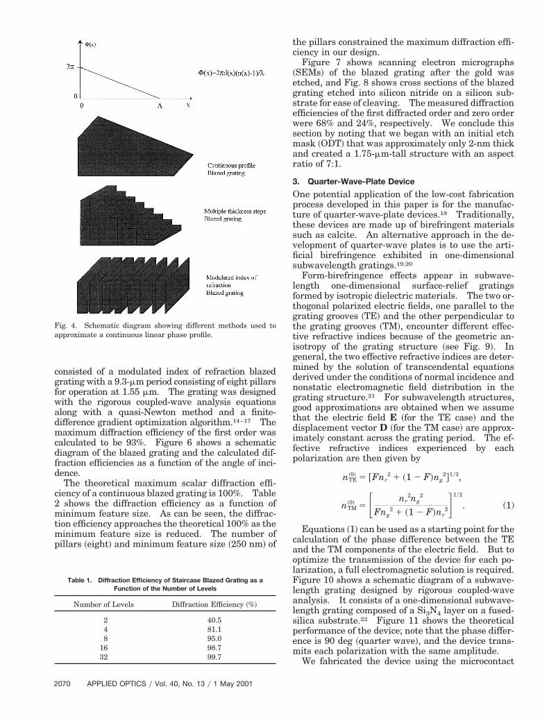
Blazed gratings9–11 are optical devices that can beused for beam deflection or wavelength dispersionapplications. The phase function of such a device isshown in Fig. 3. These are considered full phasedevices because the phase varies from 0 to 2p. Thediffraction efficiency of such a device is predicted to be100% by the paraxial scalar theory of light.
There are numerous fabrication methods used tofabricate blazed gratings. Figure 4 shows two dif-ferent methods used to approximate the continuouslinear phase profile of a blazed grating. One methodrelies on thickness variation to create the linearphase profile,12 and the other method uses a modu-lation of the local index of refraction to approximatethe linear phase profile.13
The first method is called the multiple thicknessstep method, which is based on the approximation of

tr
the continuous thickness profile as a staircase. Thediffraction efficiency depends on the number of levelsused to approximate the profile. Table 1 shows thetheoretical scalar diffraction efficiency as the numberof levels increases.
One drawback of the multiple thickness stepsmethod is that it requires more than one lithographystep and more than one etching step to obtain highdiffraction efficiencies. Each lithography step andetching step can add manufacturing errors ~align-ment between each level and thickness variation! inhe fabrication of the device. The number of levels iselated to the number of lithography steps by N 5 2M,
where M is the number of lithography steps. Thus,to fabricate an eight-level blazed grating, three li-thography steps are required.
Fig. 1. Schematic diagram of ODT after it has been patterned bymicrocontact printing on a gold-coated substrate.
Fig. 2. Master stamp fabrication process. PECVD, plasma-enhSCCM, cubic centimeters per minute at STP; MIBK:IAA, methyl
The second method is called the modulating indexof refraction method, which is based on the creation ofa modulating index of refraction profile across oneperiod of the device. This is accomplished when oneperiod of the device is divided into subwavelengthintervals such that the light beam senses a differentindex of refraction in each of the different subwave-length intervals. The advantage of the modulatingindex of refraction method is that it requires only onelithography step. One disadvantage is that the lastsubwavelength interval usually contains a pillar witha high aspect ratio.
We fabricated a beam deflector using the microcon-tact printing method described in Fig. 5. The design
chemical vapor deposition; PMMA, poly ~methyl methacrylate!;tyl ketone:isopropyl alcohol.
Fig. 3. Linear phase profile of blazed grating ~beam deflector!.
ancedisobu
1 May 2001 y Vol. 40, No. 13 y APPLIED OPTICS 2069
wad
tc
~egsewsmar
ttigmdng
difp
m
2
consisted of a modulated index of refraction blazedgrating with a 9.3-mm period consisting of eight pillarsfor operation at 1.55 mm. The grating was designed
ith the rigorous coupled-wave analysis equationslong with a quasi-Newton method and a finite-ifference gradient optimization algorithm.14–17 The
maximum diffraction efficiency of the first order wascalculated to be 93%. Figure 6 shows a schematicdiagram of the blazed grating and the calculated dif-fraction efficiencies as a function of the angle of inci-dence.
The theoretical maximum scalar diffraction effi-ciency of a continuous blazed grating is 100%. Table2 shows the diffraction efficiency as a function ofminimum feature size. As can be seen, the diffrac-tion efficiency approaches the theoretical 100% as theminimum feature size is reduced. The number ofpillars ~eight! and minimum feature size ~250 nm! of
Fig. 4. Schematic diagram showing different methods used toapproximate a continuous linear phase profile.
Table 1. Diffraction Efficiency of Staircase Blazed Grating as aFunction of the Number of Levels
Number of Levels Diffraction Efficiency ~%!
2 40.54 81.18 95.0
16 98.732 99.7
070 APPLIED OPTICS y Vol. 40, No. 13 y 1 May 2001
he pillars constrained the maximum diffraction effi-iency in our design.
Figure 7 shows scanning electron micrographsSEMs! of the blazed grating after the gold wastched, and Fig. 8 shows cross sections of the blazedrating etched into silicon nitride on a silicon sub-trate for ease of cleaving. The measured diffractionfficiencies of the first diffracted order and zero orderere 68% and 24%, respectively. We conclude this
ection by noting that we began with an initial etchask ~ODT! that was approximately only 2-nm thick
nd created a 1.75-mm-tall structure with an aspectatio of 7:1.
3. Quarter-Wave-Plate Device
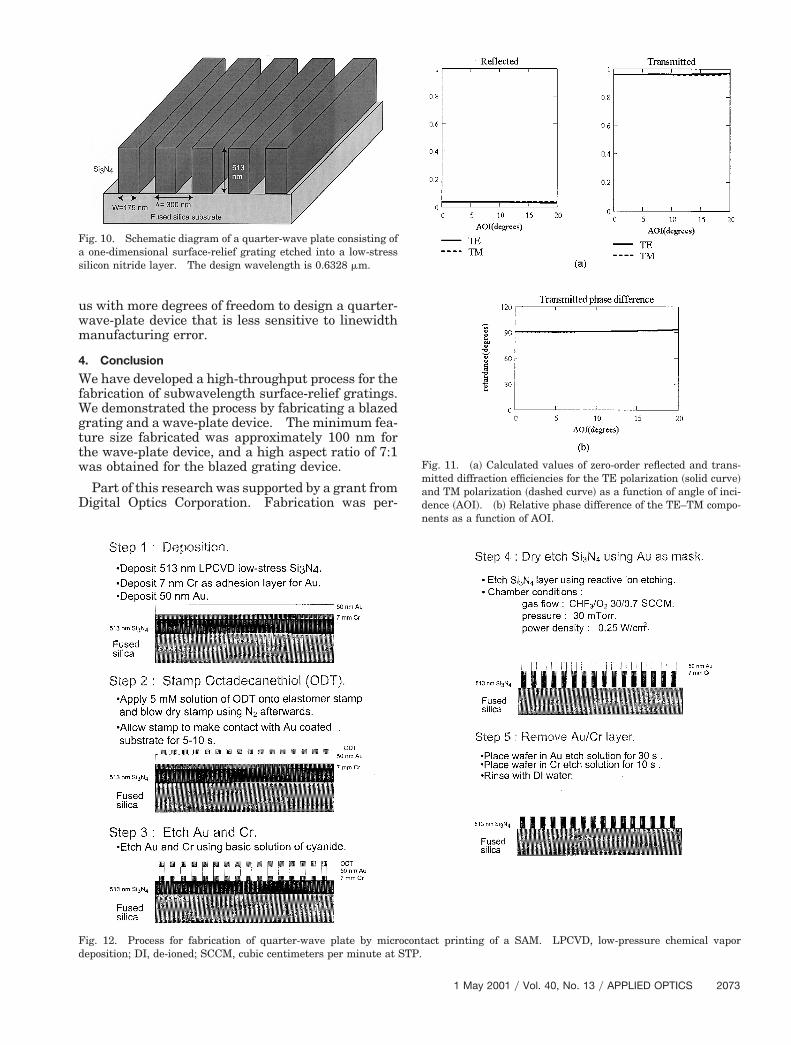
One potential application of the low-cost fabricationprocess developed in this paper is for the manufac-ture of quarter-wave-plate devices.18 Traditionally,these devices are made up of birefringent materialssuch as calcite. An alternative approach in the de-velopment of quarter-wave plates is to use the arti-ficial birefringence exhibited in one-dimensionalsubwavelength gratings.19,20
Form-birefringence effects appear in subwave-length one-dimensional surface-relief gratingsformed by isotropic dielectric materials. The two or-thogonal polarized electric fields, one parallel to thegrating grooves ~TE! and the other perpendicular tohe grating grooves ~TM!, encounter different effec-ive refractive indices because of the geometric an-sotropy of the grating structure ~see Fig. 9!. Ineneral, the two effective refractive indices are deter-ined by the solution of transcendental equations
erived under the conditions of normal incidence andonstatic electromagnetic field distribution in therating structure.21 For subwavelength structures,
good approximations are obtained when we assumethat the electric field E ~for the TE case! and the
isplacement vector D ~for the TM case! are approx-mately constant across the grating period. The ef-ective refractive indices experienced by eacholarization are then given by
nTE~0! 5 @Fnr
2 1 ~1 2 F!ng2#1y2,
nTM~0! 5 F nr
2ng2
Fng2 1 ~1 2 F!nr
2G1y2
. (1)
Equations ~1! can be used as a starting point for thecalculation of the phase difference between the TEand the TM components of the electric field. But tooptimize the transmission of the device for each po-larization, a full electromagnetic solution is required.Figure 10 shows a schematic diagram of a subwave-length grating designed by rigorous coupled-waveanalysis. It consists of a one-dimensional subwave-length grating composed of a Si3N4 layer on a fused-silica substrate.22 Figure 11 shows the theoreticalperformance of the device; note that the phase differ-ence is 90 deg ~quarter wave!, and the device trans-
its each polarization with the same amplitude.We fabricated the device using the microcontact

gvdt f
printing method as described in Fig. 12. Figure 13shows SEMs taken of the fabricated wave plate.
We then tested the device to verify that it per-formed as a wave plate. We used a He–Ne laseroperating at 632.8 nm that was linearly polarized at45 deg with respect to the slow axis of the wave plate.Thus the light coming out of the wave plate should becircularly polarized. To verify this, we inserted alinear polarizer at the output end and monitored thesignal with a detector as we rotated the output linearpolarizer. Figure 14 shows a schematic of the testsetup and the output signal from the detector. Byperforming a least-squares fit to the data, we calcu-lated the retardance to be 60 deg. Figure 15 showsthe theoretical calculation of the retardance as afunction of the duty cycle ~linewidth per period! of therating. As can be seen from Fig. 15, the retardancealue decreases as the linewidth increases, and theevice is sensitive to geometric variations. One wayo make the design less sensitive to the structure is to
Fig. 5. Deep-etch process used to create the modulated index ofdeposition; DI, de-ionized; SCCM, cubic centimeters per minute a
use a grating region composed of a multilayer thin-film stack. Figure 16 shows a schematic diagram ofa quarter-wave-plate device composed of a multilayerthin-film grating region and the theoretical calcula-tion of the retardance of this new device. As can beseen from Fig. 16, the multilayer film stack provides
ction blazed grating. PECVD, plasma-enhanced chemical vapor.
Table 2. Diffraction Efficiency for the Eight-Pillar Blazed Grating as aFunction of Minimum Feature Sizea
MinimumFeature ~nm!
DiffractionEfficiency ~%!
450 23.9400 53.2350 74.3250 92.850 93.0
aThe grating material is a 1.75-mm-thick silicon nitride film on aused-silica substrate. The grating period is 9.3 mm.
refrat STP
1 May 2001 y Vol. 40, No. 13 y APPLIED OPTICS 2071

2
Fig. 6. ~a! Schematic diagram of the modulated index of refrac-tion blazed grating. The one-dimensional surface-relief gratinghas a design wavelength of 1.55 mm. The grating material is a1.75-mm-thick film of Si3N4. ~b! Calculated diffraction efficienciesof blazed grating for the 21, 0, and 11 orders for TM polarization.AOI, angle of incidence.
Fig. 7. SEMs of the blazed grating after the gold layer was etched.
072 APPLIED OPTICS y Vol. 40, No. 13 y 1 May 2001
Fig. 8. SEMs of the blazed grating consisting of eight pillars withdifferent widths over one period etched in a Si3N4 thin film.
Fig. 9. Schematic diagram of the cross section of a one-dimensional surface-relief grating illuminated at normal inci-dence.
dn
us with more degrees of freedom to design a quarter-wave-plate device that is less sensitive to linewidthmanufacturing error.
4. Conclusion
We have developed a high-throughput process for thefabrication of subwavelength surface-relief gratings.We demonstrated the process by fabricating a blazedgrating and a wave-plate device. The minimum fea-ture size fabricated was approximately 100 nm forthe wave-plate device, and a high aspect ratio of 7:1was obtained for the blazed grating device.
Part of this research was supported by a grant fromDigital Optics Corporation. Fabrication was per-
Fig. 10. Schematic diagram of a quarter-wave plate consisting ofa one-dimensional surface-relief grating etched into a low-stresssilicon nitride layer. The design wavelength is 0.6328 mm.
Fig. 12. Process for fabrication of quarter-wave plate by micrdeposition; DI, de-ioned; SCCM, cubic centimeters per minute at
ocontact printing of a SAM. LPCVD, low-pressure chemical vaporSTP.
Fig. 11. ~a! Calculated values of zero-order reflected and trans-mitted diffraction efficiencies for the TE polarization ~solid curve!and TM polarization ~dashed curve! as a function of angle of inci-
ence ~AOI!. ~b! Relative phase difference of the TE–TM compo-ents as a function of AOI.
1 May 2001 y Vol. 40, No. 13 y APPLIED OPTICS 2073

2
formed at the Cornell Nanofabrication Facility,which is supported by the National Science Founda-tion, Cornell University, and Industrial Affiliates.Ali G. Lopez thanks the Eastman Kodak Companyfor its continuing financial support.
References1. Y. Xia and G. M. Whitesides, “Soft lithography,” Angew. Chem.
Int. Ed. Engl. 37, 550–575 ~1998!.2. J. L. Wilbur, A. Kumar, H. A. Biebuyck, E. Kim, and G. M.
Whitesides, “Microcontact printing of self-assembled monolay-ers: applications in microfabrication,” Nanotechnology 7,452–475 ~1996!.
3. T. K. Whidden, D. Ferry, M. N. Kozicki, E. Kim, A. Kumar, J.Wilbur, and G. M. Whitesides, “Pattern transfer to silicon bymicrocontact printing and RIE,” Nanotechnology 7, 447–451~1996!.
4. A. Kumar and G. M. Whitesides, “Features of gold havingmicrometer to centimeter dimensions can be formed through acombination of stamping with an elastomeric stamp and an
Fig. 13. SEMs of the quarter-wave plates fabri
074 APPLIED OPTICS y Vol. 40, No. 13 y 1 May 2001
alkanethiol ink followed by chemical etching,” Appl. Phys.Lett. 63, 2002–2004 ~1993!.
5. J. L. Wilbur, E. Kim, Y. Xia, and G. M. Whitesides, “Litho-graphic molding: a convenient route to structures with sub-micrometer dimensions,” Adv. Mater. 7, 649–652 ~1995!.
6. P. M. St. John and H. G. Craighead, “Microcontact printingand pattern transfer using trichlorosilanes on oxide sub-strates,” Appl. Phys. Lett. 68, 1022–1024 ~1996!.
7. A. Kumar, H. A. Biebuyck, and G. M. Whitesides, “Patterningself-assembled monolayers: applications in material science,”Langmuir 10, 1498–1511 ~1994!.
8. H. A. Biebuyck, N. B. Larsen, E. Delamarche, and B. Michel,“Lithography beyond light: microcontact printing with mono-layer resits,” IBM J. Res. Dev. 41, 159–170 ~1997!.
9. H. Dammann, “Blazed synthetic phase-only holograms,” Optik31, 95–104 ~1970!.
10. M. E. Warren, R. E. Smith, G. A. Vawter, and J. R. Wendt,“High-efficiency subwavelength diffractive optical element inGaAs for 975 nm,” Opt. Lett. 20, 1441–1443 ~1995!.
11. Z. Zhou and T. Drabik, “Optimized binary, phase-only, diffrac-
by different processes as explained in the text.
cated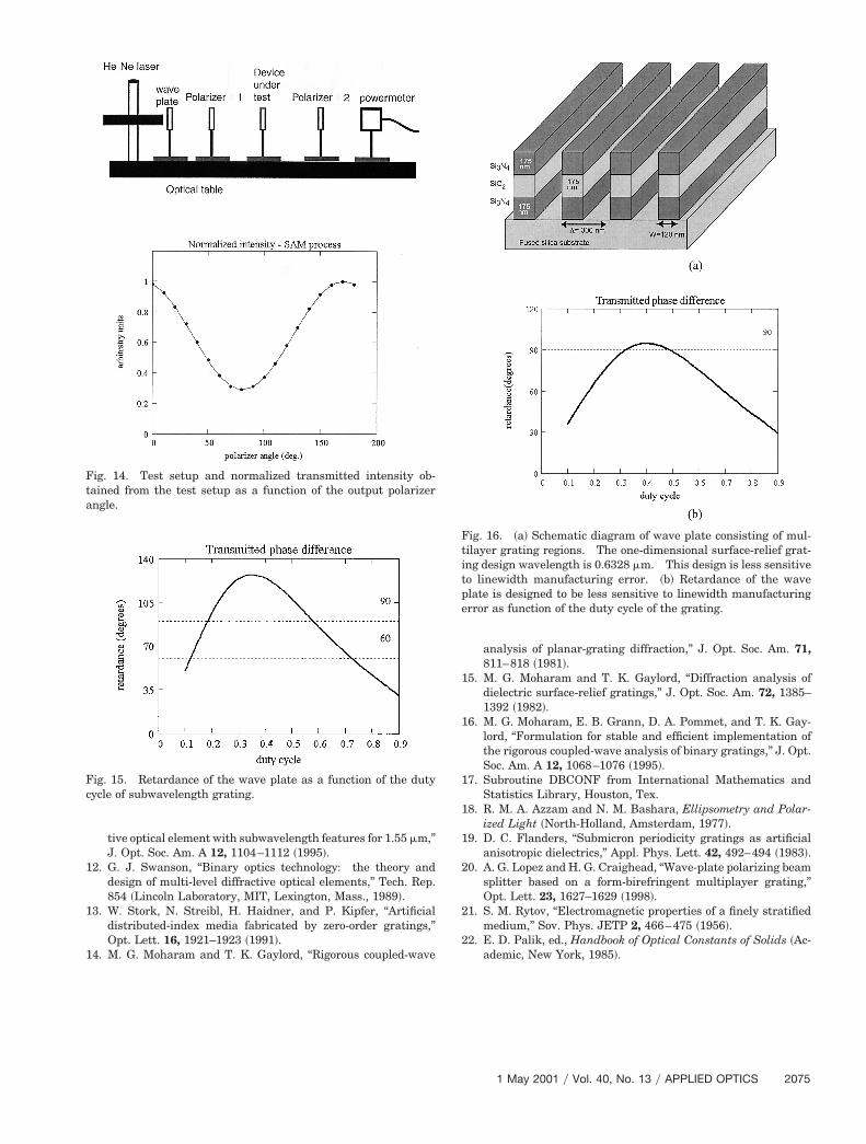
tive optical element with subwavelength features for 1.55 mm,”J. Opt. Soc. Am. A 12, 1104–1112 ~1995!.
12. G. J. Swanson, “Binary optics technology: the theory anddesign of multi-level diffractive optical elements,” Tech. Rep.854 ~Lincoln Laboratory, MIT, Lexington, Mass., 1989!.
13. W. Stork, N. Streibl, H. Haidner, and P. Kipfer, “Artificialdistributed-index media fabricated by zero-order gratings,”Opt. Lett. 16, 1921–1923 ~1991!.
14. M. G. Moharam and T. K. Gaylord, “Rigorous coupled-wave
Fig. 14. Test setup and normalized transmitted intensity ob-tained from the test setup as a function of the output polarizerangle.
Fig. 15. Retardance of the wave plate as a function of the dutycycle of subwavelength grating.
analysis of planar-grating diffraction,” J. Opt. Soc. Am. 71,811–818 ~1981!.
15. M. G. Moharam and T. K. Gaylord, “Diffraction analysis ofdielectric surface-relief gratings,” J. Opt. Soc. Am. 72, 1385–1392 ~1982!.
16. M. G. Moharam, E. B. Grann, D. A. Pommet, and T. K. Gay-lord, “Formulation for stable and efficient implementation ofthe rigorous coupled-wave analysis of binary gratings,” J. Opt.Soc. Am. A 12, 1068–1076 ~1995!.
17. Subroutine DBCONF from International Mathematics andStatistics Library, Houston, Tex.
18. R. M. A. Azzam and N. M. Bashara, Ellipsometry and Polar-ized Light ~North-Holland, Amsterdam, 1977!.
19. D. C. Flanders, “Submicron periodicity gratings as artificialanisotropic dielectrics,” Appl. Phys. Lett. 42, 492–494 ~1983!.
20. A. G. Lopez and H. G. Craighead, “Wave-plate polarizing beamsplitter based on a form-birefringent multiplayer grating,”Opt. Lett. 23, 1627–1629 ~1998!.
21. S. M. Rytov, “Electromagnetic properties of a finely stratifiedmedium,” Sov. Phys. JETP 2, 466–475 ~1956!.
22. E. D. Palik, ed., Handbook of Optical Constants of Solids ~Ac-ademic, New York, 1985!.
Fig. 16. ~a! Schematic diagram of wave plate consisting of mul-tilayer grating regions. The one-dimensional surface-relief grat-ing design wavelength is 0.6328 mm. This design is less sensitiveto linewidth manufacturing error. ~b! Retardance of the waveplate is designed to be less sensitive to linewidth manufacturingerror as function of the duty cycle of the grating.
1 May 2001 y Vol. 40, No. 13 y APPLIED OPTICS 2075