sumec energy holdings co., ltd. - university of new south ... · pdf filemetal assisted...
TRANSCRIPT
NANJING . CHINA 2017.03
SUMEC Energy Holdings Co., Ltd.

P A R T 1
About us
P A R T 2
R&D Progress
P A R T 3
PV Plant case
Research and development of advanced photovoltaic technologies at Phono Solar: Black
silicon, MWT and SHJ

PART 1. About us SINOMACH
SUMEC Group & SUMEC Energy Holdings Co., Ltd.
SINOMACH New Energy Research Institute
Page 3

About SINOMACH
Established in January 1997
A class state-owned enterprise
Fortune Global 500 enterprises
180+ overseas branches
35.1 billion USD business revenue
Over 120,000+ employees
R&D and Manufacture
Trade and Services
Project Contracting
Financing &Investment
Core business
Page 4

About SUMEC
Established in 1978
A key member of SINOMACH
Central government-owned
enterprises in Jiangsu province
5.7 billion USD business revenue
10,000+ employees
Core business
Trade & service
Investment & development
R&D & Engineering
Page 5
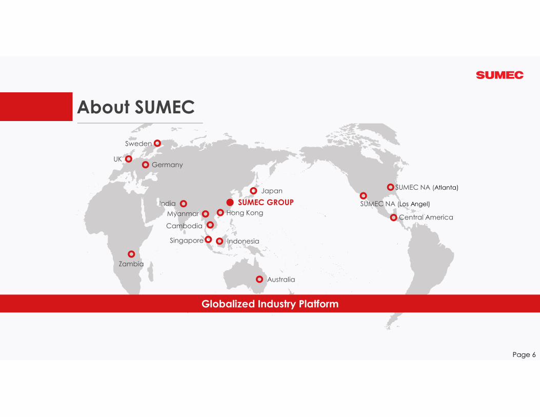
UK
Globalized Industry Platform
Australia
IndonesiaSingapore
Zambia
Cambodia
SUMEC GROUP
Japan
Hong KongMyanmar
India
Germany
Sweden
Central America
SUMEC NA (Atlanta)
SUMEC NA (Los Angel)
About SUMEC
Page 6

About SUMEC
Solar EnergyMarine
EngineeringComplete Sets of
EngineeringPower Generation
Equipment
Textile & ApparelMechanical &
ElectronicWind Energy
Geothermal Energy
Power Tools
Page 7

About SUMEC Energy
SUMEC Energy, a leading global provider of
clean energy solutions, committed to customer
centered solutions for Energy Supply, Energy
Management, Energy Saving and Energy Storage
SUMEC Energy in order to provide efficient and
economically sustainable solutions, uses extensive
and innovated supply chain strategies, principles
and techniques
Global shipments
3500MW
Domestic projects
1500MW
Reduction of standard coal
3.9 million
tons/y
Generating capacity
3.5 billion
kwh/y
Page 8

About SINOMACH New Energy Research Institute
Solar Module
System
Operation & Maintenance
Characterization
The Internet of Things
Solar Cell
A close loop capability system for reducing the
cost per kilowatt hour of PV generated power
Page 9

R&D
Manufacturing
Pearl River Economic Zone
Yangtze River Economic Zone
Beijing-Tianjin-Hebei Economic Zone
LED lighting manufacture / Shenzhen
PV cells manufacture / Xuzhou 1GW
Desert testing field / Xinjiang
Wind power testing field / Inner MongoliaStorage solutions research and manufacture / Tianjin
Smart PV management platform development / Shanghai
PV modules manufacture / Nanjing, Yancheng 800MW
Tropics testing field / Haikou
R&D and Manufacturing Base
Page 10

Manufacturing
PV Module Maker Tiering System
1Tier
Phono Solar Technology Co., Ltd., was founded by SUMEC
Group Corporation. Phono Solar is leading brand in the
clean energy industry, providing high efficiency PV modules
since 2004.
Global shipments
3500MW
Production capacity
1000MW
Page 11

PART 2. R&D Progress Strategy & Technology Roadmap
Metal Wrap Through Technology
HJT Technique & Performance
Nano-Texturing
PERC+ Research
Page 12
PV System Forecasting

Proven Technique, Cost Effective, Lots of Mass Production Data, Highly Material and Tools Dependent
Pilot Technique, Strong Potential of Cost Down & Efficiency Gain, Small Scale of Investment
More Cost, Higher Efficiency Gain, Cost of Ownership Still in Proving
RD Stage Technique or Failed Technique, Future Technique
Lower Risk, Cost Effective
Higher Risk Worse CoO
Page 13
Strategy & Technology Roadmap
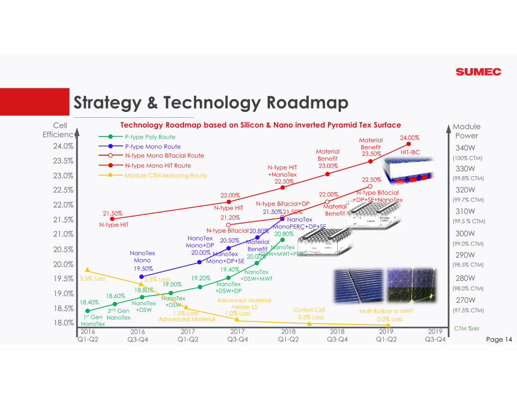
Strategy & Technology Roadmap
2016Q1-Q2
1st Gen NanoTex
CTM %rel
300W
290W
280W
(98.0% CTM)
Module Power
(98.5% CTM)
(99.0% CTM)
310W(99.5 % CTM)
320W(99.7% CTM)
330W(99.8% CTM)
340W
(100% CTM)
2017Q1-Q2
2017Q3-Q4
2018Q1-Q2
2018Q3-Q4
2019Q1-Q2
2019Q3-Q4
18.40%
Technology Roadmap based on Silicon & Nano inverted Pyramid Tex Surface
2016Q3-Q4
18.0%
18.5%
19.0%
CellEfficiency
19.5%
20.0%
20.5%
21.0%
21.5%
22.0%
22.5%
23.0%
23.5%
24.0%
18.60%18.80%
19.00%19.20%
19.40%
20.00%
20.80%
19.50%
20.00%
20.50%
20.80%
21.50%21.50%
22.00% 22.00%
21.20%21.50%
22.50%22.50%
23.00%
23.50%
24.00%
2nd Gen NanoTex
NanoTex+DSW
NanoTex+DSW
NanoTex+DSW+DP
NanoTex+DSW+MWT
NanoTex Mono
NanoTex Mono+DP
NanoTex Mono+DP+SE
NanoTex MonoPERC+DP+SE
Material Benefit
N-type Bifacial
N-type Bifacial+DP
N-type Bifacial+DP+SE+NanoTex
Material Benefit
N-type HIT
N-type HIT+NanoTex
Material Benefit
HIT-IBC
Material Benefit
3.5% Loss 2.5% Loss
1.5% Loss 1.0% Loss0.5% Loss 0.0% LossAdvanced Material
Advanced Material+Wider LS
Multi Busbar or MWTCutted Cell
N-type HIT
N-type Mono HIT Route
N-type Mono Bifacial Route
P-type Mono Route
P-type Poly Route
Module CTM reducing Route
270W
(97.5% CTM)
NanoTex+DSW+MWT+PERC
Page 14

Nano-Texturing
Femtosecond Laser EtchingNano spike structure,high cost,surface damage
Metal Assisted Chemical Etching (MACE)Nanowires or nanopores,anisotropic etching,low cost
Reactive Ion Etching (RIE)Nanocones or nanopillars,plasma etching,high equipment cost
Electrochemical EtchingPorous structure,complex process
Page 15

Nano-Texturing
Page 16
Schematic diagram of the experimental setup for the flexible black silicon fabrication
Femtosecond Laser Etching
Scanning electron microscope (SEM) imageof the micro spike structure of the fabricatedflexible black silicon
Reactive Ion Etching (RIE)
Schematic illustration of a DC-plasma immersion ion implantation apparatus
SEM images of silicon surface structures formed by RIE processing with different SF6/O2
gas flow ratios

Nano-Texturing
Page 17
Metal Assisted Chemical Etching (MACE)
Schematic of Nano-textured silicon processing steps.
Ag-assisted etching Structure rebuild Metal Deposition
Etching
Metal RemovalReconstruction
Clean

Nano-Texturing
Page 18
Voc(V) Isc(A) Rs(mΩ) FF(%) Eff(%)
Acid textured(avg.) 0.630 8.647 0.0029 78.61 17.59%
Alkaline treatment Nano-mc-Si(avg.)
0.629 8.738 0.0024 79.19 17.89%
Round treatment Nano-mc-Si(avg.)
0.630 8.764 0.0029 79.02 17.94%
Best Nano-mc-Si 0.634 8.882 0.0023 79.78 18.47%
0
10
20
30
40
50
60
70
80
90
100
0
10
20
30
40
50
60
70
80
90
100
300 500 700 900 1100
R%
IQE %
Wavelength nm
Quantum efficiency for Nano-Tex vs normal Multi

Nano-Texturing
Page 19
Inverted pyramid structure by NSR
Nano Structure Rebuilding (NSR) solutionBased on acid systemH2O2 and additive
SEM images of the nanostructure after NSR treatment under different time
SEM images of the inverted pyramids with further NSR treatment
Nano-Texturing
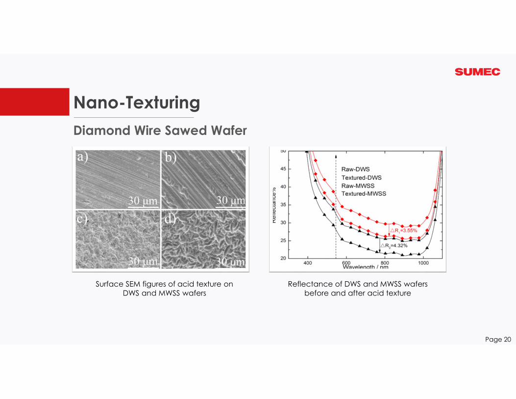
Page 20
Surface SEM figures of acid texture on DWS and MWSS wafers
Reflectance of DWS and MWSS wafers before and after acid texture
Diamond Wire Sawed Wafer
Nano-Texturing
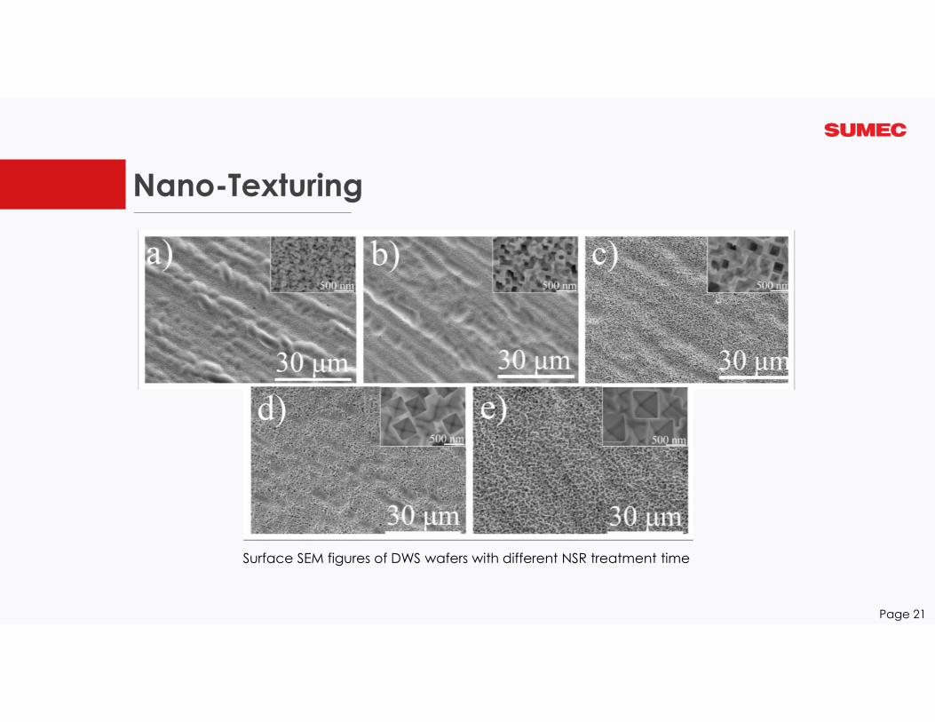
Page 21
Surface SEM figures of DWS wafers with different NSR treatment time
Nano-Texturing
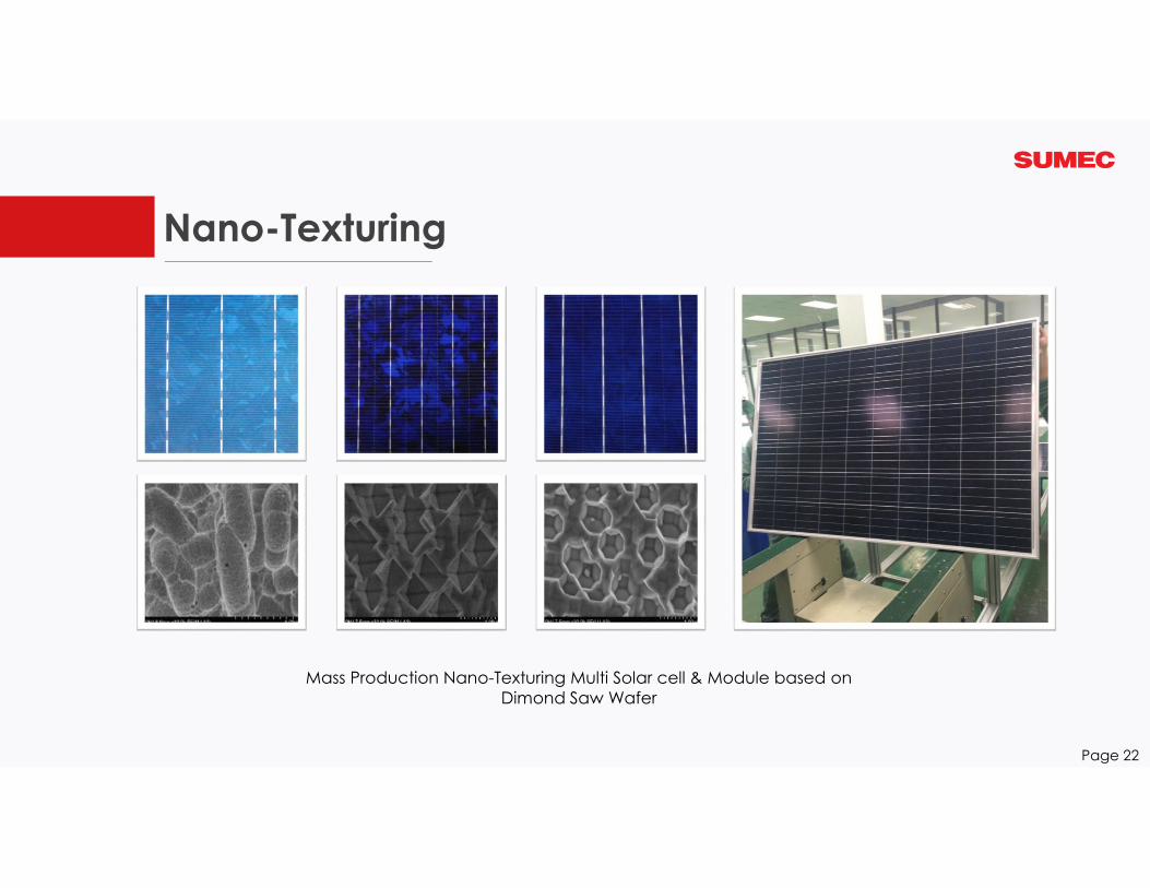
Page 22
Mass Production Nano-Texturing Multi Solar cell & Module based on Dimond Saw Wafer

Nano-Texturing
Page 23
Acid TexIrregular
NanowiresNano-Holes
Inverted Pyramid
Football like
Structure
Index for SUMEC’s Nano-Tex Solar Cell
Cell
1) Cell Cost Down 5%
2) Compatible with DWS wafer
3) Compatible with other High
Efficiency Technologies
4) Efficiency Gain 0.4%
Module
System1) Power Output Gain
(kwh/kw) is over 3%
2) System Cost Down 3%
1) Module Cost Down 4%
Acid Tex Nano-Tex
Chemical($/W) 0.002 0.006
Tool, Consumption, Labour Cost ($/W)
0.0007 0.002
Total Cost($/W) 0.0027 0.008
Cost Saving from Wafer($/W)
0(Slurry) 0.013(Diamond)
The Real Cost Down or Increase($/W)
0.0027(Increase) 0.005(Down)
Efficiency Gain 0% +0.4%
Income($/W) — 0.023
Total Income($/W) — 0.028
Module Cost — 3.5% (Down)
System Cost — 2.4% (Down)
Power Cost per Kwh — 5% (Down)

Nano-Texturing
Page 24
Time/Capacity
Normal Multi 260PNano-Tex
260P Nano-Tex/NormalArray #1
(1510KW)Array #2(1510KW)
Array #3(1510KW)
Array #4(1510KW)
Avg(1510KW)
Array #5(1478KW)
Jul 110.577 110.065 110.094 108.673 109.852 112.735 2.62%
Aug 114.499 113.878 113.808 111.573 113.440 116.709 2.88%
Sep 128.228 127.055 127.057 122.925 126.316 132.354 4.78%
Oct 103.370 102.733 102.809 100.124 102.259 106.659 4.30%
Nov 43.769 43.510 43.554 42.891 43.431 44.704 2.93%
Dec 73.595 72.822 73.136 71.169 72.680 75.053 3.26%
Sum 647.631 642.884 643.594 628.524 640.658 663.267 3.53%
Power Plant: SUMEC Bao Fengda YangZhou; Location: (33.37786N,119.52888E)Type: Ground-based solar system; Capacity: 9MW
Power Plant: SUMEC HQ; Location: NanjingType: distributed system; Capacity: 1.1MW
2.92%
3.55%3.24%
3.48%3.47%3.45%3.37%
3.98%
3.29%3.56%
0.00%
1.00%
2.00%
3.00%
4.00%
5.00%
6.00%
0.00%
2.00%
4.00%
6.00%
8.00%
10.00%
12.00%
Mar Apr May Jun Jul Aug Sep Oct Nov Dec
Sunny Cloud Shower Overall
Power Output Benefits Per KWatts Module
Nano-Texturing
Page 25
Technical Indicator Mass Production 2nd Generation
Tools
Through put(pc/H) 3400 5000+
Uptime 88% 92%
Investment ($) 430,000 580,000
Automation fully fully
Process
Wafer Cutting Slurry & diamond Slurry & diamond
Wafer multi & mono multi & mono
Efficiency Gain(multi) 0.4%(19.00%) 0.4%(19.00%)
Module
CTM ~1.5% , +5 ~ +10W ~1% , +10W
Reliability & Stability good good
Power Output per KW Gain
+3% +3%

Metal Wrap Through Technology
Page 26
MWT Contrast items Normal
Wrapped-through Cell Structure Front electrode
No busbar
Front Grid
Busbar
Better appearancemonotonous appearance
Less Grid Shading More
+0.3% Efficiency Gain 0%
Patterned conductive foil integrated backsheet
Module assembling
normal backsheet
Electrical conductive adhesive(Less CTM)
Welding strip(Higher Rs Loss)
Compatible with IBC & thin wafer
None Compatible with IBC & thin wafer
Front Sheet
Encapsulant
Encapsulant & BackSheet
Front Sheet
Encapsulant
Encapsulant
Back Sheet

Metal Wrap Through Technology
Page 27
Mono 60pcs MWT module(Normal Mono ~ 280Wp, MWT
Mono ~ 295Wp)
Multi 60pcs MWT module(Normal Multi ~ 270Wp, MWT
Multi ~ 285Wp)
Front side 25 holes by laser drilled → Future 36 holes
Average efficiency for normal multi wafer & process → 19.0%
We are doing process integration with Nano-Tex multi cells,
the average cell efficiency might achieve over 19.5%
Our power output target for the 60p@module is 300Wp

Metal Wrap Through Technology
Page 28
MWT reliability & stability test
DH Condition:
1000hours@85℃ & 85%RH
TC Condition:
85 ℃ ~ -40℃ ~ 85℃ @200hours
TC 600hours by PI-Berlin
Damp-Heat Test 1000hours Thermal-Cycle Test 200hours
Power output gain by better heat transfer performance
+3% gain

Metal Wrap Through Technology
Page 29
P-Type wafer start
Laser drilling of vias
Damage etching & texturing
POCl3 diffusion in furnace
Etching paste printing & dry
PSG/etching paste/rear removal
SixNy coating & passivation
Screen printing & cofiring
Testing & sorting
P-Type wafer start
Damage etching & texturing
POCl3 diffusion in furnace
PSG/rear removal
SixNy coating & passivation
Screen printing & cofiring
Testing & sorting
Normal Screen Printing Process vs. MWT
After drilling holes
A big end up holes
Is better for paste’s
filling, which is
necessary for hole
junction removal step
and contact printing
process

Metal Wrap Through Technology
Page 30
“MWT + Nano-Tex” Technology
Strategic Partner : Sunport
Module Capacity: 500 GW in Xuzhou City

HJT Technique & Performance
Page 31
Type N Type HIT P Type
Advantages
1. No LID & No PID
2. Lower temperature
coefficient
3. Bifacial structure
4. Higher conversion efficiency,
easier over 22%
1. Mature process flow
2. More supplier for mass
production
3. Lower cost
Disadvantages
1. Higher process requirement
2. Small process windows
3. Cost more for tools and
material
1. Some LID & PID issue
2. Hard to achieve efficiency
over 22%
Advantages & Disadvantages between N type HJT & P type
Cell Type P-Poly P-Mono N-HIT
Cell Efficiency 19% 21% 22%
Ideal module efficiency
17.22% 18.68% 19.57%
CTM loss 1-2% 3.5-4% <2%
Real module efficiency
16.87% 17.94% 19.18%
LID 1% 2% N
PID Y Y N
Temperature coefficient (%/℃)
-0.45 -0.45 -0.27
PTC/STC 89.20% 89.00% 93.00%
Efficient module efficiency
14.60% 15.33% 17.83%
HJT Technique & Performance
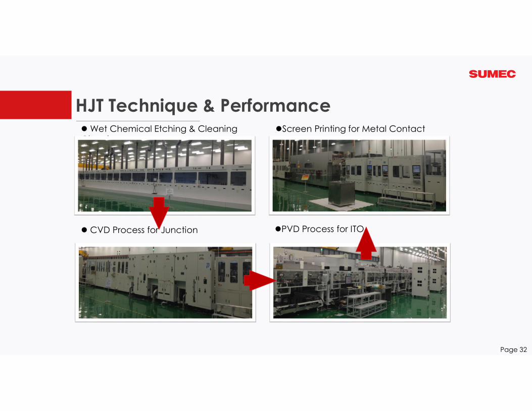
Page 32
Wet Chemical Etching & Cleaning Cleaning
CVD Process for Junction
Screen Printing for Metal Contact
PVD Process for ITO

HJT Technique & Performance
Page 33
Items Progress Result Comment Optimization Plan
CTM DoneAverage CTM 3.35%
The range is 3.17%~3.74%For mono P type production,
CTM avg is 3.5%
1.Use high transparent glass2.Optimize the soldering process
3.Refining the sorting BIN
LID Done30─35kWh be stable,1.9%,range:1.2%~2.8%
Higher than P mono1.Retest the sample
2. Change different simulator
Temperature Coefficient
Doneα=0.02%,β=-0.28%
δ=-0.32%Normal P type cell: 0.02%/℃、-
0.32%/℃、-0.46%/℃
Low Irradiation Done 200W/m2 : ↓80.8% P type average: ↓80.5%
DH Done DH1000, ↓2.19%IEC61215 & internal control rule:
after DH2000, TC400, Power degradation < 5%, no
appearance issueTC Done TC400, ↓3.54%
Some crack happened near the beginning of solder strip

HJT Technique & Performance
Page 34
HJT bifacial power generating performance testing site

HJT Technique & Performance
Page 35
HJT bifacial module power generation site experiment with different landform (one year data)
Landform Power output kWh kWh/W Power output gain Analysis Future Plan
White backsheet 316.99 0.0545 1.15 (15%)
Result highly fit the reflection coefficient
of the landform
White paint & white stone might be a cost effective solution for increasing the Rearside light absorbing
White paint 314.21 0.05375 1.13 (13%)
White stone 309.19 0.0529 1.12 (12%)
Water 297.26 0.0508 1.07 (7%)
Cement (baseline) 276.24 0.0474 1.00
Grass 267.54 0.0461 0.97
HJT single side module vs. HJT bifacial
Module type Power output kWh kWh/W Power output gain Analysis Future Plan
Single side 176.42 0.0304 1.038(3.8%) Backsheet reflectance is considerable for
single side HJT
Compare black and white backsheetBifacial 170.74 0.0293 1.00
HJT single side module vs. Normal P type poly
Module type Power output kWh kWh/W Power output gain Analysis*
HJT single side 176.42 0.0304 1.045(4.5%) 1、gain from the backside (backsheet reflectance)2、lower temperature coefficient. (HIT-0.32%)(P type-0.46%)。Normal 155.03 0.0291 1.00

PERC+ Research
Page 36
p-PERC Contrast items PERC+
Yes Rear SixNy layer No
Yes Laser grooving No
About 20nm(TMA consumption higher)
Al2O3 (TMAconsumption)
About 6nm(TMA consumption lower)
No Bifacial cell Yes (bifacial coefficient>75%)20.5% Conversion efficiency 20.3%(lab result )
Full print , high Al paste consumption Grid print ,low
0
20
40
60
80
100
300
340
380
420
460
500
540
580
620
660
700
740
780
820
860
900
940
980
1020
1060
1100
EQE
PERC+-front PERC+-back
0
20
40
60
80
100
300
340
380
420
460
500
540
580
620
660
700
740
780
820
860
900
940
980
1020
1060
1100
IQE-Front
PERC+-front IQE PERC+-front R
0
20
40
60
80
100
300
340
380
420
460
500
540
580
620
660
700
740
780
820
860
900
940
980
1020
1060
1100
IQE-Back
PERC+-back IQE PERC+-back R
PERC+ -frontJsc (mA/cm^2) 39.0
PERC+ -backJsc (mA/cm^2) 24.3
PERC+ process and performance research

PV System Forecasting
Page 37
Location
(longitude and
latitude、altitude、
terrain)
Illumination
(SolarGIS satellite data)Pvsyst Simulation
System design
optimization(angle、
DC/AC、different loss)
Forecasting of System
SolarGIS Data + Pvsyst Simulation + Empirical Correction

PV System Forecasting
Page 38
0
5
10
15
20
25
30
1 3 5 7 9 11 13 15 17 19 21 23 25 27 29
SolarGIS GTI(MJ/m2) Kipp&Zonen GTI(MJ/m2)
The Satellite Data is not very
accuracy especially there is any
microclimate change ate the
location.
So, we installed high accurate
Solar radiation measurement
tools to fix SolarGIS’ data.
PART 3. PV Plant case Ground Mounted PV Plant
Distributed Power Plant
Others
Page 39

Marketing Strategy
Page 40
Distributed Systems on Rooftops
Abandoned Ground-Mounted (seashore, coal-mining subsidence area)
Standalone System
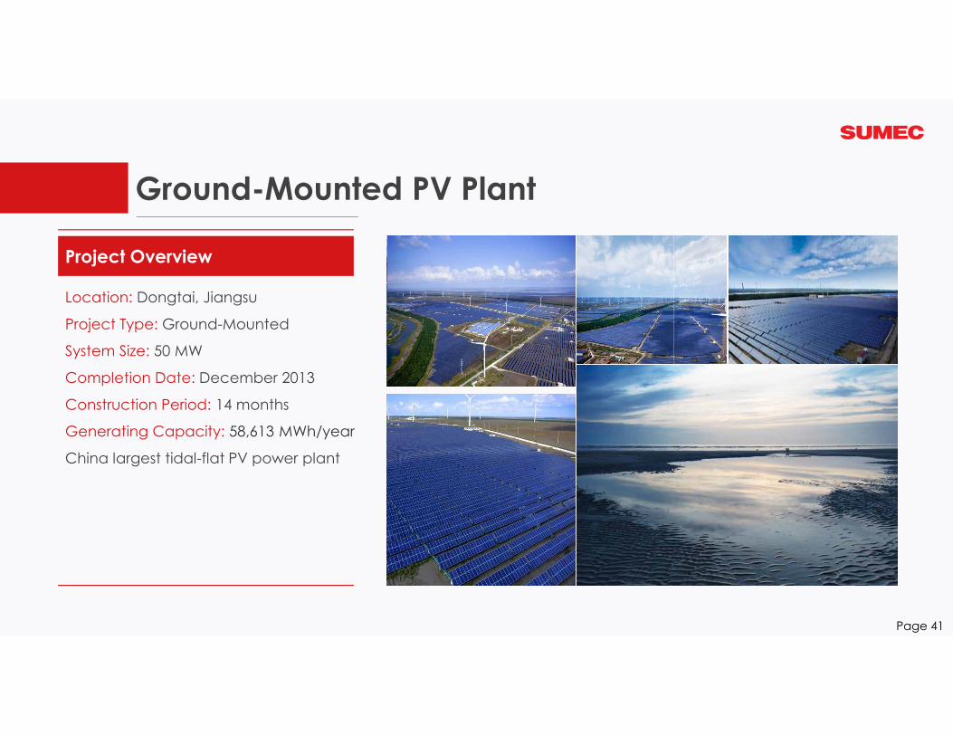
Ground-Mounted PV Plant
Page 41
Location: Dongtai, Jiangsu
Project Type: Ground-Mounted
System Size: 50 MW
Completion Date: December 2013
Construction Period: 14 months
Generating Capacity: 58,613 MWh/year
China largest tidal-flat PV power plant
Project Overview

Distributed Power Plant
Page 42
Location: Hefei, Anhui
Project Type: Distributed Rooftop
System Size: 100 MW
Completion Date: May 2016
Construction Period: 24 months
Generating Capacity: 48,930 MWh/year
China largest Distributed PV power plant
Project Overview

Others
Page 43
Xuyi, 9.8MW.hilly area, sheep farming
Peixian, 15.8MW.Coal mining subsidence area

Others
Page 44
Germany America
JapanAustrilia

NANJING . CHINA
THANKS