sunny days ahead
TRANSCRIPT
Sunny Days Ahead
1
Preface
For entrepreneurs and businesses exploring opportunities in the solar PV domain, power
production opportunities are the most apparent. Opportunities available along the other
parts of the solar PV value chain, especially in the manufacturing sector are much less in the
limelight.
While power production as a business opportunity has its attractions, especially taking into
account the National Solar Mission (NSM) incentives, this is essentially a PPA-based
business model, with little upside potential. On the other hand, in order for India to
become a leader in solar power sector, it is imperative that India is able to develop a strong
supporting eco-system to support the growth in solar PV power production. Of prime
importance to this support eco-system is the role of manufacturing activities within the solar
PV value chain.Unlike the power production opportunities, manufacturing opportunities
bring with them the possibility of higher innovation and significantly higher upsides.
In order to participate in these opportunities, and to take critical investment decisions, a
better understanding of these is essential for Indian businesses.The objective of this white
paper is to provide inputs and intelligence for the manufacturing activities in India for the
solar PV ecosystem – for both crystalline and thin film technologies.
EAI is India’s leading research and consulting group with a dedicated focus on the Indian
renewable energy sector. The white paper has been developed by EAI as a part of the
Solarcon India 2011 by SEMI, held at Hyderabad in November2011.
Narasimhan Santhanam
Director
Energy Alternatives India

Sunny Days Ahead
2
Sunny Days Ahead
3
Contents
INTRODUCTION .......................................................................................................................................... 5
POTENTIAL IN INDIA ..................................................................................................................................................................... 6
RESOURCE ASSESSMENT .............................................................................................................................................................. 6
REGIONAL POTENTIAL .................................................................................................................................................................. 7
PV TECHNOLOGIES ..................................................................................................................................... 8
CRYSTALLINE SILICON (C-SI) ....................................................................................................................................................... 8
THIN FILM (TF) ............................................................................................................................................................................. 8
COMPARISON BETWEEN CRYSTALLINE AND THIN FILM PANELS ............................................................................................. 9
SOLAR PV MANUFACTURING SCENARIO ............................................................................................. 16
CRYSTALLINE SILICON ................................................................................................................................................................ 16
Polysilicon ............................................................................................................................................................................ 17
Wafer ..................................................................................................................................................................................... 19
Cells........................................................................................................................................................................................ 20
Modules ............................................................................................................................................................................... 21
THIN FILMS .................................................................................................................................................................................. 22
Amorphous Silicon (a-Si) ............................................................................................................................................... 22
Cadmium Telluride (CdTe) ............................................................................................................................................ 23
Copper Indium Gallium (di)Selinide (CIGS) ............................................................................................................ 23
OTHER MANUFACTURING OPTIONS......................................................................................................................................... 24
Raw Material, Machineries and Equipment for Core Products ...................................................................... 24
Non-core Solar Products ............................................................................................................................................... 29
CENTRAL AND STATE POLICY ANALYSIS................................................................................................................................... 30
Central .................................................................................................................................................................................. 30
State Policy ......................................................................................................................................................................... 32
CONCLUSION ............................................................................................................................................. 33
ANNEXURE I ............................................................................................................................................... 34
ANNEXURE II ............................................................................................................................................. 37
ANNEXURE III ............................................................................................................................................ 38
EAI - ASSISTING YOUR COMPANY FOR ATTRACTIVE MANUFACTURING OPPORTUNITIES IN
SOLAR PV ................................................................................................................................................... 43
ABOUT SEMI AND PV GROUP ................................................................................................................. 47
Sunny Days Ahead
4
Highlights
Polysilicon
Currently, there is no polysilicon manufacturing capacity in India
To sustain 20 GW worth of installations, over 14,000 MT per year of polysilicon
manufacturing capacity would be required
Wafer
There is currently no wafer manufacturing company in India with significant
production capacity
To sustain 20 GW worth of targeted installations, over 2000 MW per year of
wafer manufacture would be required
Cells
Local content requirements will ensure robust demand for local cell
manufacturing
Stimulus for domestic cell manufacturing will not only be from the Central
policy, but also from some state policies promoting domestic manufacture
and vertical integration
Modules
Significant growth in domestic module uptake is expected in India; however,
this is not being exploited by Indian module makers owing to uncompetitive
prices
Vertical integration is the key factor that determines the cost-competitiveness
of solar modules
While thin films have as high an acceptance level in India as crystalline silicon
module, thin films do not have as much competition
Production Equipment
77% of the Indian manufacturing capacity is expected to be powered by turn-
key lines, indicating significant promise for this sector in terms of
manufacturing and system integration
Sunny Days Ahead
5
Introduction
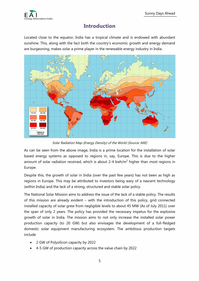
Located close to the equator, India has a tropical climate and is endowed with abundant
sunshine. This, along with the fact both the country’s economic growth and energy demand
are burgeoning, makes solar a prime player in the renewable energy industry in India.
Solar Radiation Map (Energy Density) of the World (Source: AltE)
As can be seen from the above image, India is a prime location for the installation of solar
based energy systems as opposed to regions in, say, Europe. This is due to the higher
amount of solar radiation received, which is about 2-4 kwh/m2 higher than most regions in
Europe.
Despite this, the growth of solar in India (over the past few years) has not been as high as
regions in Europe. This may be attributed to investors being wary of a nascent technology
(within India) and the lack of a strong, structured and stable solar policy.
The National Solar Mission aims to address the issue of the lack of a stable policy. The results
of this mission are already evident – with the introduction of this policy, grid connected
installed capacity of solar grew from negligible levels to about 45 MW (As of July 2011) over
the span of only 2 years. The policy has provided the necessary impetus for the explosive
growth of solar in India. The mission aims to not only increase the installed solar power
production capacity (to 20 GW) but also envisages the development of a full-fledged
domestic solar equipment manufacturing ecosystem. The ambitious production targets
include
2 GW of Polysilicon capacity by 2022
4-5 GW of production capacity across the value chain by 2022
Sunny Days Ahead
6
Potential in India
Theoretically, about 5000 trillion kWh/m2 of solar energy is incident across the entire area of
the country, with daily averages of incident radiation falling between 4 and 7 kWh/m2/day.
While the theoretical potential stated seems like a large number, the actual potential is
significantly lower due to various constraints such as:
Available area for plant development
Useful solar energy capture area within the power plant
Theoretical conversion efficiency limits for solar PV based systems
Resource Assessment
The solar resource map of India has been developed using data extrapolated from satellite
imagery.The areas with the highest potential for solar based power generation are
concentrated in the peninsular region of the country – with Rajasthan being the only
noteworthy exception.About 1.75 million sq. km of land receives an annual irradiation of
about 5.5 to 6 kWh/m2/day. In addition to this, about 1.1 million sq. km of land receives
irradiation between 5 and 5.5 kWh/m2/day putting the total available (optimal) area for
setting up solar power plants at about 1.85 million square km.
Why resource assessment matters
Accurate site comparison and selection
Energy estimates can be made with greater confidence
Predicting financial viability (a function of revenue and hence electricity generated)
Increasing the bankability of the project
Performance validation
Utility forecasting and grid interfacing
Relative uncertainties for resource assessments1 (Source: AWSTruepower)
1 Satellite Modelled Data is what is commonlyused. GHI – Global Horizontal Irradiance data is what is
applicable to solar PV power plants and is measured on the ground (at the site) using a pyranometer
Sunny Days Ahead
7
As such, the accuracy of this information is not very high. Furthermore, data in some regions
with high suitability for solar power plants are available only at very low spatial resolutions
undermining the accuracy of it even more.
A key hindrance to the growth of solar power in India is the lack of availability of accurate
irradiation data. The lack of this information severely limits a developer’s capability to
accurately predict the amount of electricity which a plant is expected to generate and hence
the revenues he is expected to accrue. This is one of the major factors that has stunted new
investment in the solar energy sector.
Regional Potential
Regional potential of each state in India can be viewed from two angles – actual insolation
incident on the state and the state specific policy adopted. Ideally, the state with the highest
potential would have an intersection of the two.
Insolation Driver
A look at the solar insolation map of India shows that the southern states of Andhra Pradesh,
Karnataka, Tamil Nadu and states in north western India such as Gujarat, MP and Rajasthan
have the best solar radiation in the country. States such as Arunachal Pradesh, Haryana,
Jharkhand, Kerala, Orissa, Punjab, Uttar Pradesh and West Bengal also have reasonable
potential, but there is very little installed capacity in these regions.
Policy Driver
The key driver for region specific growth is not just the amount of solar insolation the
state receives, but the presence of a strong state solar policy.As of August 2011, only
three states have come up with concrete solar specific polices. These include – Gujarat,
Rajasthan and Karnataka.The Tamil Nadu and Maharashtra governments are expected to
come up with their state solar policy soon.
Of these, the Gujarat and Rajasthan state policies are the ones that are both aggressive and
ambitious, with Gujarat looking to add close to 1 GW of solar PV in the coming years.Due to
the policy, regulatory support and higher solar insolation, Gujarat and Rajasthan are likely to
be the hotbeds for solar PV development in India in the short term.
Sunny Days Ahead
8
PV Technologies
Solar PV systems can be broadly classified into two types based on the type of technology
employed
Crystalline Silicon (c-Si)
Thin Film (TF)
Crystalline Silicon (c-Si)
These solar cells are manufactured from bulk crystalline silicon material known as MGSi. This
raw material, through various processes is converted to semiconducting wafers which
generate electricity when exposed to solar radiation through a process known as the
photovoltaic effect.
Among the various technologies available, c-Si based generation is the oldest and most
mature electricity generation system. Based on the crystalline structure of the ingot/wafer
used, c-Si based modules are further divided into the following categories
Monocrystalline
Polycrystalline or Multicrystalline
Monocrystalline modules are more expensive than multicrystalline modules but at the same
time they are more efficient i.e. they produce more electricity per watt of installed capacity.
Thin Film (TF)
Thin film technologies evolved as a result of low polysilicon availability for the manufacture
of c-Si based modules. Thin film modules are typically characterised by their lower material
requirement for the manufacture of a photoactive layer. Due to the lower grade and quantity
of raw materials used, these modules are usually less efficient when compared to c-Si based
modules. These modules are significantly cheaper due to the lower material cost coupled
with the fact that there are fewer steps involved in the manufacturing process.
The lower efficiencies as well as other drawbacks are being overcome using more exotic
materials and diverse manufacturing processes. Based on the type of material used for cell
manufacture, TFPV can be further classified as
Amorphous Silicon (a-Si)
Cadmium Telluride (CdTe)
Copper Indium Gallium (di)Selinide (CIGS)
Sunny Days Ahead
9
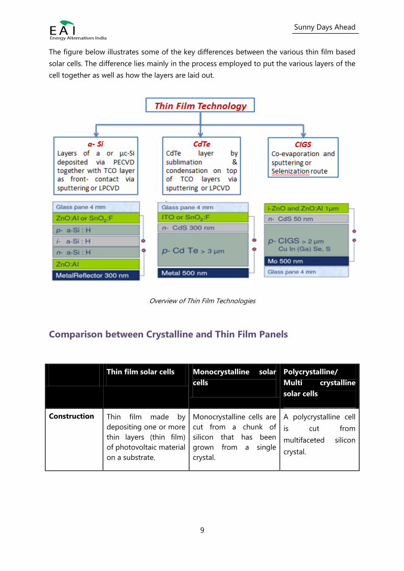
The figure below illustrates some of the key differences between the various thin film based
solar cells. The difference lies mainly in the process employed to put the various layers of the
cell together as well as how the layers are laid out.
Overview of Thin Film Technologies
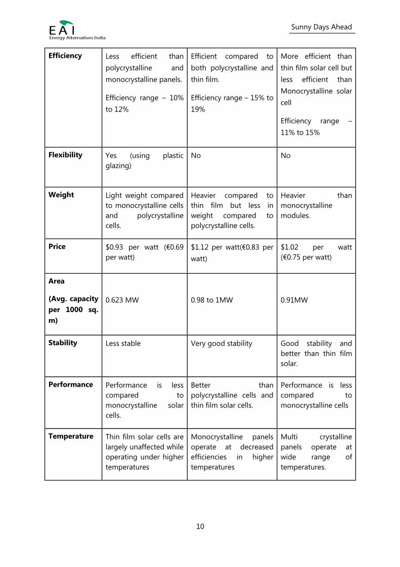
Comparison between Crystalline and Thin Film Panels
Thin film solar cells Monocrystalline solar
cells
Polycrystalline/
Multi crystalline
solar cells
Construction
Thin film made by
depositing one or more
thin layers (thin film)
of photovoltaic material
on a substrate.
Monocrystalline cells are
cut from a chunk of
silicon that has been
grown from a single
crystal.
A polycrystalline cell
is cut from
multifaceted silicon
crystal.
Sunny Days Ahead
10
Efficiency
Less efficient than
polycrystalline and
monocrystalline panels.
Efficiency range – 10%
to 12%
Efficient compared to
both polycrystalline and
thin film.
Efficiency range – 15% to
19%
More efficient than
thin film solar cell but
less efficient than
Monocrystalline solar
cell
Efficiency range –
11% to 15%
Flexibility Yes (using plastic
glazing)
No No
Weight Light weight compared
to monocrystalline cells
and polycrystalline
cells.
Heavier compared to
thin film but less in
weight compared to
polycrystalline cells.
Heavier than
monocrystalline
modules.
Price $0.93 per watt (€0.69
per watt)
$1.12 per watt(€0.83 per
watt)
$1.02 per watt
(€0.75 per watt)
Area
(Avg. capacity
per 1000 sq.
m)
0.623 MW
0.98 to 1MW
0.91MW
Stability Less stable Very good stability Good stability and
better than thin film
solar.
Performance Performance is less
compared to
monocrystalline solar
cells.
Better than
polycrystalline cells and
thin film solar cells.
Performance is less
compared to
monocrystalline cells
Temperature Thin film solar cells are
largely unaffected while
operating under higher
temperatures
Monocrystalline panels
operate at decreased
efficiencies in higher
temperatures
Multi crystalline
panels operate at
wide range of
temperatures.

Sunny Days Ahead
11
Market Share
Currently, c-Si dominates the global PV cell manufacturing segment with a share of about
83% of the total cell production. It is expected that the market share for thin film
technologies is expected to increase significantly with estimates pegging the number
between 21% and 29% by 20122.
With falling c-Si prices (estimates suggest that the price could drop below $1 per Wp by
20143), thin film’s market share would depend on
Maintaining the cost savings advantage offered by thin films (i.e. the absolute price
difference between thin films and c-Si modules has to be maintained. Thus thin film
module prices have to drop to match the crashing c-Si prices). This is the primary
factor that makes thin film technologies bankable as opposed to c-Si due to the lack
of availability of reliable information over the project life.
Improving efficiency of thin film cells
Reduction in balance of system costs associated with thin film based power plants
Higher rates of adoption in developing countries – mainly in Asia, Africaand South
America(owing to better suitability to higher temperature conditions in addition to
lower capital requirements)
Market share of various technologies (Source: GTM Research)
The Indian Context
It is interesting to note that this global trend does not necessarily apply to India. For
instance, of the 30 winners (28 of whom achieved financial closure) under Phase 1
Batch 1 of the National Solar Mission, 50% of the winners went with c-Si and the other
50% went with thin film.
2 Source: GTM Research
3 Source: iSuppli
Sunny Days Ahead
12
The primary factors driving this trend could be attributed to
Lower capital costs associated with thin film based power plants
Ease of availability and lower cost of landand lower labour BoS cost (lower labour,
project management, civil and construction costs) for setting up power plants
Availability of better financing options from foreign banks (E.g. Ex-Im bank offers
cheap loans at lower interest rate when procuring modules from US manufacturers).
Technology Suitability for India
Bankability
Banks tend to prefer well established technologies, with a proven track record for financing
projects. In view of this and the fact that the solar energy sector in itself is in a nascent stage
in India, c-Si has the upper hand considering the technology has been around for around 30
years meaning it is has proven credentials for a time period equal to the entire operational
life of a power plant.
However, in case of thin film, as the technology is new it does not have a proven track
record. Thus the performance of the system cannot be guaranteed over the lifetime of
operation of the power plant. This makes the system prone to heavier scrutiny frombanks.
Land Requirement
One of the prime criteria for selection of technology for a power plant is the availability of
suitable land (both in the qualitative and quantitative sense) to setup the power plant. Thin
film technologies typically require more land than c-Si based systems due to their lower
power density. However, in India, large tracts of land are readily available (at cheap rates
when compared with project costs), nullifying the advantage offered by c-Si in this regard. In
this scenario, the project cost becomes the limiting factor tipping the scales in favour of thin
films.
Project Cost
The overall project cost plays a major role in the final decision to go ahead with investment
as it lays the foundation for determining the profitability of the project. The project cost can
be considered to be the sum of two components – the modules and the balance of systems
cost.
Module Cost – this attributes to about 60% of the project cost. In this respect, thin
films hold the advantage.c-Si modules are about 25% to 40% more expensive per Wp
when compared with thin film4.
4 Source: EnergyTrend

Sunny Days Ahead
13
Capital Cost Breakup for Solar PV
BoS Cost – this component, in most cases forms the rest of the project cost of any
power plant. In this respect, c-Si holds the advantage. In general, BoS costs are about
9% higher for thin film technologies when compared to c-Si technologies5. However
in the Indian context, the BoS costs play a subdued role in choice of technology due
to lower labour, project management, civil and construction costs.
Comparison of BoS Costs Between c-Si and Thin Film Based Systems (Source: GTM Research)
The cost savings from module offsets the additional BoS cost requirement for thin film,
thus making the overall project cost of thin film based systems lower than that of c-Si
systems or in the worst case, comparable.
5 Source: GTM Research
1%
52%
22%
9%
7%
2%
7%
Capital Cost Breakup for Solar PV
Land
PV Modules
PCU
Civil & General Works
Mounting Structures
Evacuation Cost
Preliminary & PreoperativeExpenses
Sunny Days Ahead
14
Alternative Financing
Alternate financing mechanisms are available for projects which import modules from
foreign countries. For instance Ex-Im, OPIC, EDC etc. offer attractive financing options at
lower interest rates for import of modules from USA and Canada respectively. In view of this,
more project developers are looking to import modules from abroad.
However, with JNNSM acting as the most popular (preferred) framework for solar
development in India, this route may be taken by thin film technologies alone. This is a direct
result of the local content requirement enforced by the policy which (as of Phase I, Batch II) is
applicable only to c-Si based power generation.
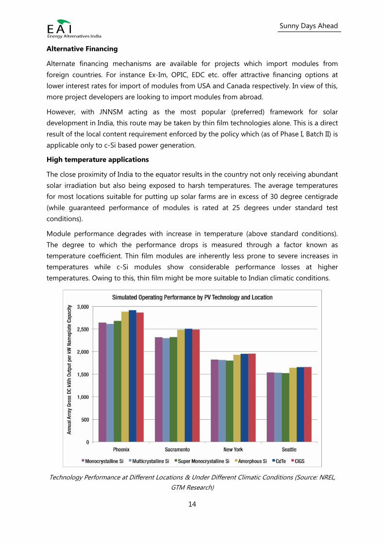
High temperature applications
The close proximity of India to the equator results in the country not only receiving abundant
solar irradiation but also being exposed to harsh temperatures. The average temperatures
for most locations suitable for putting up solar farms are in excess of 30 degree centigrade
(while guaranteed performance of modules is rated at 25 degrees under standard test
conditions).
Module performance degrades with increase in temperature (above standard conditions).
The degree to which the performance drops is measured through a factor known as
temperature coefficient. Thin film modules are inherently less prone to severe increases in
temperatures while c-Si modules show considerable performance losses at higher
temperatures. Owing to this, thin film might be more suitable to Indian climatic conditions.
Technology Performance at Different Locations & Under Different Climatic Conditions (Source: NREL,
GTM Research)
Sunny Days Ahead
15
A recent study6 showed that thin film modules produced significantly more electricity (about
5% more in favour of thin films)per unit of installed capacityin high temperature regions
(Refer figure above. Here, Phoenix experiences climatic conditions similar to most sites in
India). Some of the possible reasons for the above trend could be
Less negative temperature coefficient which gives thin film silicon modules a
performance advantage over c-Si modules at increasingly high irradiance and cell
temperatures
Better performance under diffused light conditions – the thin film silicon panels out-
perform c-Si, due to a combination of spectral and angle-of-incidence effects
Local Content Requirement
As per guidelines under Phase 1, Batch 2 of JNNSM scheme, all power plants using c-Si
based technology are required to procure their cells and modules from local manufacturers.
This could lead to a shortage of supply or out-dated, inefficient modules. However, thin film
modules are exempt from this regulation meaning that they can be procured from any
provider outside India – thus ensuring technological superiority as well as bringing in the
added experience of foreign project integrators.
Trackingand Diffuse Light Performance
Tracking systems help improve the output of a power plant by up to 10%.These systems are
more suitable for projects employing c-Si technology than thin film technology. This is
because thin film based systems generate electricity even under lower irradiance conditions
(i.e. under diffused light conditions).
Indian project developers and system integrators generally do not go for tracking systems.
This may be attributed to
Lack of technical expertise
Lack of local tracking system manufacturers (currently there is only one tracking
system manufacturer in India7)
Tracking system cost is not offset by the excess electricity generated
In view of this, it would be advisable to go for thin film based systems as their peak
performance is not dependant(to a large extent) on the presence of tracking systems.
6 Source: NREL, GTM Research
7 Source: Sunflower Solutions (www.sunflowersolutions.in/in/)
Sunny Days Ahead
16
Solar PV Manufacturing Scenario
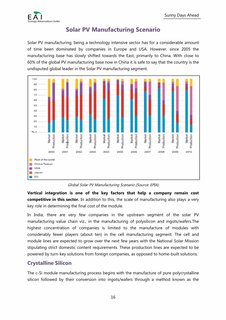
Solar PV manufacturing, being a technology intensive sector has for a considerable amount
of time been dominated by companies in Europe and USA. However, since 2005 the
manufacturing base has slowly shifted towards the East, primarily to China. With close to
60% of the global PV manufacturing base now in China it is safe to say that the country is the
undisputed global leader in the Solar PV manufacturing segment.
Global Solar PV Manufacturing Scenario (Source: EPIA)
Vertical integration is one of the key factors that help a company remain cost
competitive in this sector. In addition to this, the scale of manufacturing also plays a very
key role in determining the final cost of the module.
In India, there are very few companies in the upstream segment of the solar PV
manufacturing value chain viz., in the manufacturing of polysilicon and ingots/wafers.The
highest concentration of companies is limited to the manufacture of modules with
considerably fewer players (about ten) in the cell manufacturing segment. The cell and
module lines are expected to grow over the next few years with the National Solar Mission
stipulating strict domestic content requirements. These production lines are expected to be
powered by turn-key solutions from foreign companies, as opposed to home-built solutions.
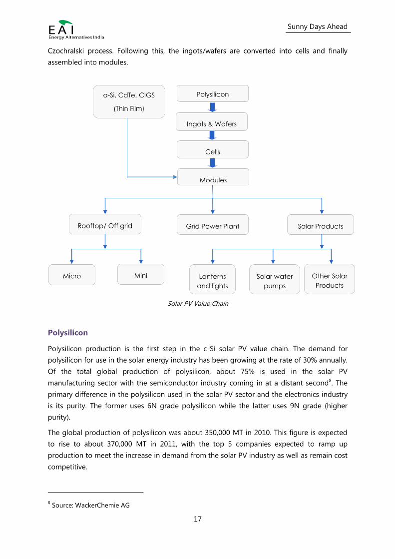
Crystalline Silicon
The c-Si module manufacturing process begins with the manufacture of pure polycrystalline
silicon followed by their conversion into ingots/wafers through a method known as the
Sunny Days Ahead
17
Czochralski process. Following this, the ingots/wafers are converted into cells and finally
assembled into modules.
Solar PV Value Chain
Polysilicon
Polysilicon production is the first step in the c-Si solar PV value chain. The demand for
polysilicon for use in the solar energy industry has been growing at the rate of 30% annually.
Of the total global production of polysilicon, about 75% is used in the solar PV
manufacturing sector with the semiconductor industry coming in at a distant second8. The
primary difference in the polysilicon used in the solar PV sector and the electronics industry
is its purity. The former uses 6N grade polysilicon while the latter uses 9N grade (higher
purity).
The global production of polysilicon was about 350,000 MT in 2010. This figure is expected
to rise to about 370,000 MT in 2011, with the top 5 companies expected to ramp up
production to meet the increase in demand from the solar PV industry as well as remain cost
competitive.
8 Source: WackerChemie AG
Polysilicon
Ingots & Wafers
Cells
Modules
Rooftop/ Off grid Grid Power Plant Solar Products
Micro Mini Lanterns
and lights
Solar water
pumps
Other Solar
Products
a-Si, CdTe, CIGS
(Thin Film)
Sunny Days Ahead
18
Capacity Global – 350,000 MT (2010). Expected to grow to 370,000 MT (2011)
Local – none
Cost of Production Current – $30 to $35 per Kg
Expected – About $25 per Kg by 2011
Production Yield 1 tonne of pure polysilicon can be obtained from 1.2 to 1.6 tonnes of MGSi
Electricity Requirement About 100 to 200 kWh per Kg
Price Current – Between $42 and $51 per Kg
Global production is dominated by the top 5 companies in the industry. Together, these
companies account for close to 75% of the total global production (refer table below).
Currently, there is no significant production of polysilicon in India. Lanco Solar, Bhaskar
Silicon and Yash Birla Group have announced plans to set up polysilicon manufacturing
plants in India.
Rank Company Country Annual Production
2010 (MT)
Expected Production
2011 (MT)
1 Hemlock
Semiconductor
USA 36,000 36,000
2 WackerChemie Germany 30,500 33,000
3 OCI Company South Korea 27,000 42,000
4 GCL-Poly China 21,000 21,000
5 REC Silicon Norway 16,000 17,500
6 MEMC USA 12,500 15,000
7 LDK China 11,000 18,000
8 Tokuyama Japan 8,200 8,200
9 M.Seteck Japan 6,000 7,000
10 Daqo New
Energy
China 3,300 4,300
List of Top Global Manufacturers of Polysilicon (Source: PV Magazine)
Sunny Days Ahead
19
Wafer
A silicon wafer is a thin slice of crystal semiconductor, such as a material made up from
silicon crystal, which is circular in shape. They are used in the manufacturing of
semiconductor devices, integrated circuits and other small devices. There are multiple
processes through which silicon wafers are manufactured. These include
Czochralski Process – for manufacture of monocrystalline ingots
Bricking/Solidification – for manufacture of multicrystalline ingots
Capacity Global – About 29 GW (2010). Expected to grow to about 42 GW (2011)
Local – none
Cost of Production Current – 25 to 50 cents per Wp
Production Yield 1 Wp equivalent of wafer requires about 6 to 7 grams of pure polysilicon
Price Multi-Si Wafer (156mm x 156mm) - $1.87 to $2.10
Mono-Si Wafer (156mm x 156mm) - $2.43 to $2.85
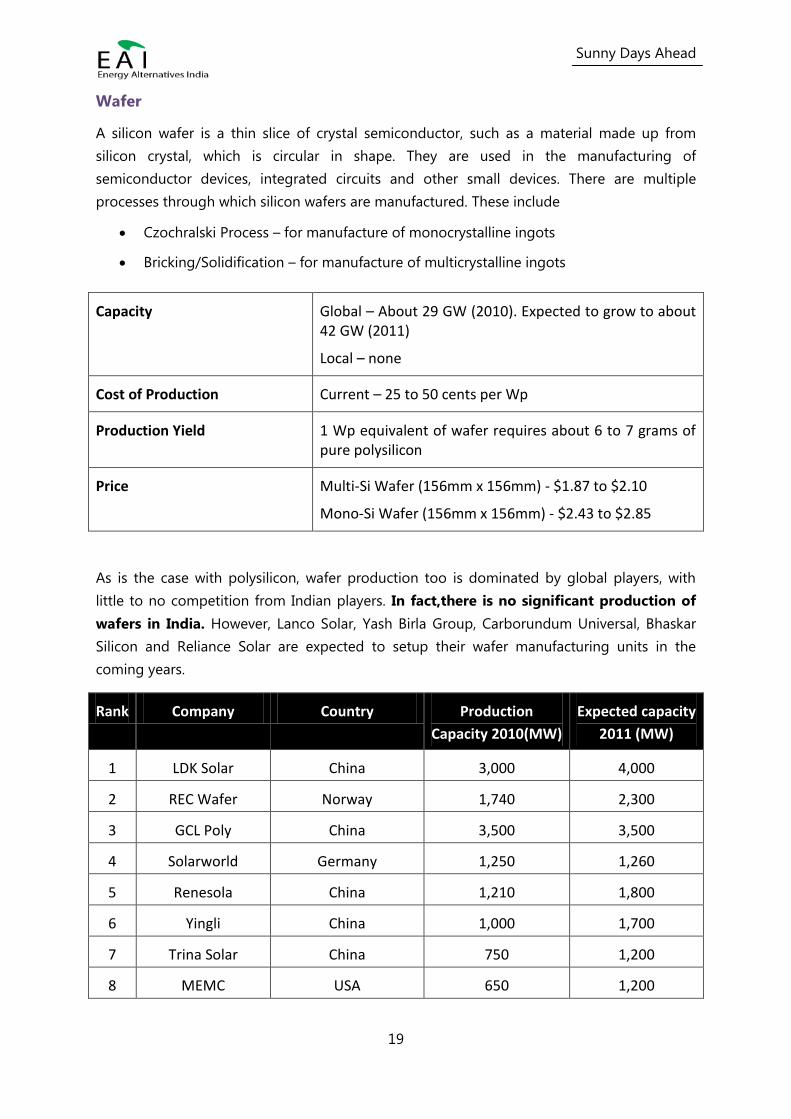
As is the case with polysilicon, wafer production too is dominated by global players, with
little to no competition from Indian players. In fact,there is no significant production of
wafers in India. However, Lanco Solar, Yash Birla Group, Carborundum Universal, Bhaskar
Silicon and Reliance Solar are expected to setup their wafer manufacturing units in the
coming years.
Rank Company Country Production
Capacity 2010(MW)
Expected capacity
2011 (MW)
1 LDK Solar China 3,000 4,000
2 REC Wafer Norway 1,740 2,300
3 GCL Poly China 3,500 3,500
4 Solarworld Germany 1,250 1,260
5 Renesola China 1,210 1,800
6 Yingli China 1,000 1,700
7 Trina Solar China 750 1,200
8 MEMC USA 650 1,200
Sunny Days Ahead
20
9 Pillar Spain 700 720
10 Green Energy tech Taiwan 800 1,500
List of Top Global Wafer Manufacturers (Source: PV Magazine)
Cells
The third step in the solar PV value chain is the manufacture of cells from the wafers. This
step involves the conversion of the wafer to a photoactive diode i.e. a piece of
semiconductor that is able to generate free electrons when exposed to sunlight.
Capacity Global – About 33 GW (2010). Expected to grow to about 48 GW (2011)
Local – About 600 MW (2010)
Cost of Production Current – 25 to 40 cents per Wp (excluding feedstock)
Price Between 70 cents and 85 cents per Wp
The total global cell manufacturing capacity is about 30 GW. As with wafers, China dominates
this segment too, with about 50% of the total global manufacturing capacity. It is interesting
to note that of the top 10 companies globally, one is a thin film cell manufacturer (FirstSolar).
Furthermore, 50% of the companies in the list manufacture both cells and modules – a move
towards vertical integration and cost cutting.
Rank Company Country Annual Production
Capacity in
2010(MW)
Actual
Production in
2010(MW)
1 Suntech China 1800 1585
2 JA Solar China 2100 1463
3 First Solar(Thin film) USA 1502 1411
4 Trina China 1200 1050
5 Q-cells(includes Thin film) Germany 1265 1014
6 Yingli China 1000 980
7 Motech Taiwan 1200 945
8 Sharp(includes Thin Film) Japan 1000 910
9 Gintech Taiwan 930 827
Sunny Days Ahead
21
10 Kyocera Japan 650
List of Top Global Cell Manufacturers (Source: Photon)
The Indian scenario for cell manufacture is not as barren as is the case for polysilicon and
wafer production. There are about 10 companies involved in cell manufacture in India (refer
Annexure I for a detailed list). The total cell manufacturing capacity of these companies
amounts to about 600 MW which is still a far cry from the available capacities the world over.
The leading companies in terms of available capacity include Indosolar, Moser Baer (thin
film), TATA BP solar and Websol.
The key thing to note with the Indian companies is that they are strictly into cell and
module manufacturing with no vertical integration. This leads to their cells and modules
not being cost competitive with the cells/modules from world leaders such as the Chinese
manufacturers.
Modules
The final step in the value chain is the assembly of the various solar cells into modules. The
process in this stage involves the interconnection and packaging of multiple cells into a
single unit. The price of a PV module is mainly influenced by the price of the cells it
incorporates.
Capacity Global – About 37 GW (2010)
Local – About 1200 MW (2010)
Production Yield Dependent on module rating. Each cell has a rating of about 4 Watts.
Price About $1.2 per Wp
The solar module manufacturing segment is highly fragmented due to the ease of
manufacturing of the module – which in essence is just an assembly process and the low
capital cost involved in setting up of the assembly line. The top global manufacturers of
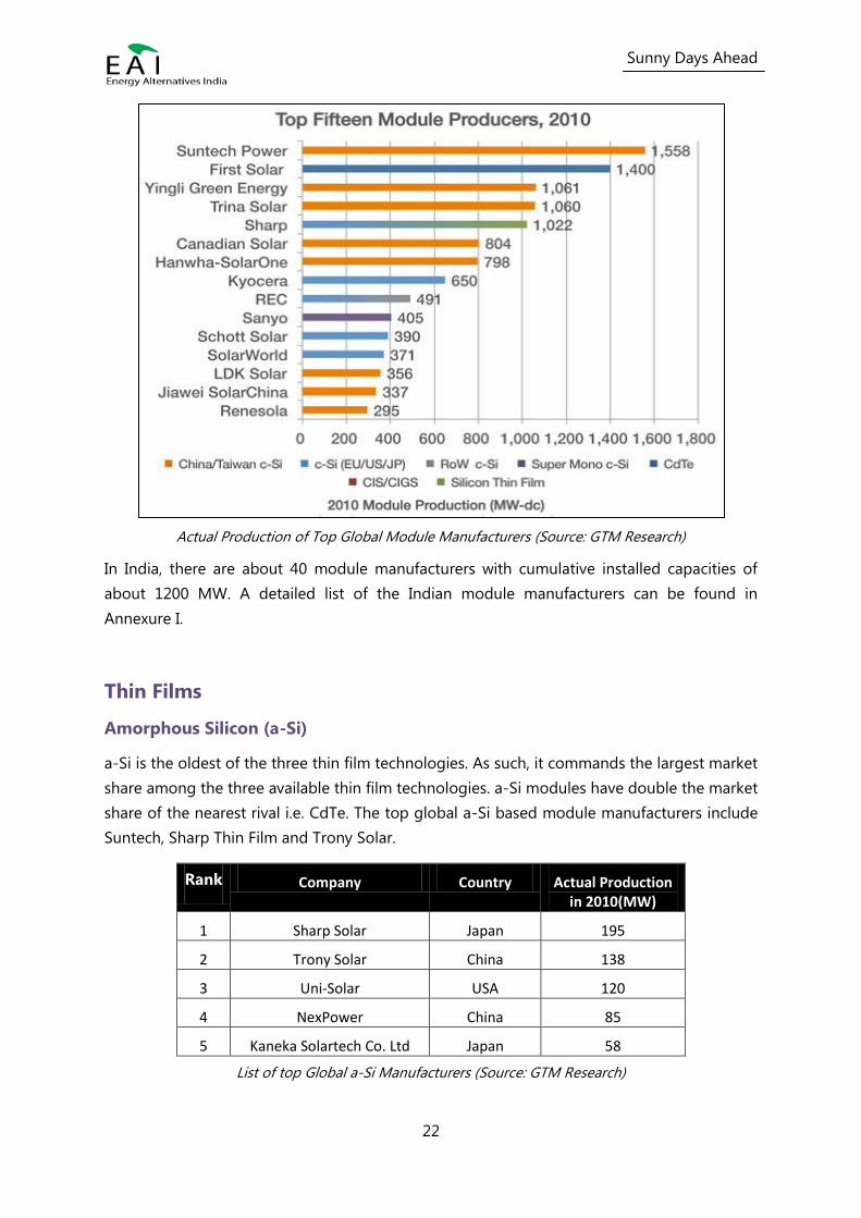
modules include Suntech Power, FirstSolar, Yingli Green Energy, Trina Solar and Sharp.
Sunny Days Ahead
22
Actual Production of Top Global Module Manufacturers (Source: GTM Research)
In India, there are about 40 module manufacturers with cumulative installed capacities of
about 1200 MW. A detailed list of the Indian module manufacturers can be found in
Annexure I.
Thin Films
Amorphous Silicon (a-Si)
a-Si is the oldest of the three thin film technologies. As such, it commands the largest market
share among the three available thin film technologies. a-Si modules have double the market
share of the nearest rival i.e. CdTe. The top global a-Si based module manufacturers include
Suntech, Sharp Thin Film and Trony Solar.
Rank Company Country Actual Production in 2010(MW)
1 Sharp Solar Japan 195
2 Trony Solar China 138
3 Uni-Solar USA 120
4 NexPower China 85
5 Kaneka Solartech Co. Ltd Japan 58
List of top Global a-Si Manufacturers (Source: GTM Research)
Sunny Days Ahead
23
In India, Moser Baer is the only company with a-Si based module manufacturing
facilities, with a production capacity of about 50 MW, making it one of the leading global
players too.
The costs associated with the manufacture of a-Si module is about $1.1 per Wp. Current
market price for a-Si modules is about $1.2 per Wp making the profit margin pretty low.
Since a-Si based solar modules have some of the lowest efficiencies compared to other solar
PV modules, in the future it is expected that pure a-Si would have very low demand. They are
scheduled to be replaced by some of the more advanced technologies such as tandem
junction cells, which employ a combination of both a-Si and c-Si technologies.
Cadmium Telluride (CdTe)
CdTe has the second highest market share of the three thin film technologies. CdTe has seen
significant growth mainly due to the aggressive push by US based FirstSolar who have a
virtual stranglehold on the CdTe (as well as the thin film) market. Their module production
capacity was about 1400 MW in 2010. To put their dominance in perspective, the next closest
company, Sharp (which manufactures a-Si based thin film modules) has a capacity of about
195 MW.
Rank Company Country Annual Production Capacity in 2010 (MW)
1 First Solar USA 1400
2 Abound Solar USA 65
3 PrimeStar Solar USA 30
4 Calyxo GmbH Germany 25
List of Top Global CdTe Manufacturers
Some of the other players in the CdTe segment are Abound Solar, Primestar Solar and Calyxo
GmbH. Currently, there are no manufacturing units producing CdTe based modules in India.
The cost of production of a CdTe module is about $0.8 per Wp while the market sale price is
close to $1 per Wp. This makes CdTe based modules one of the cheapest modules available
in the market. Further, FirstSolar has stated that the price of the modules could fall to about
$0.75 per Wp by 2012.
Copper Indium Gallium (di)Selinide (CIGS)
Of the three thin film technologies, CIGS is the newest. The advantage of CIGS is that it does
not use any toxic or rare earth materials during the manufacturing process. Thus CIGS is
Sunny Days Ahead
24
expected to be the future of Thin Film based solar power generation systems if it can remain
cost competitive.
The cost of production of a CIGS module varies between $1.2 and $1.3 per Wp while the
selling price is about $1.4 per Wp making it the most expensive thin film based generation
system. However, there is significant potential for cost reduction considering the nascent
nature of the technology.
A significant portion of the total installed production capacity (about 800 MW) is attributed
to Solar Frontier. Other global production companies include Nanosolar, Avancis and Solibro
Solar (a subsidiary of Q-Cells).
In India, Shurjo Energy has a production capacity of about 7 MW9. No other company
manufactures CIGS based modules in India, as of September 2011.
Other Manufacturing Options
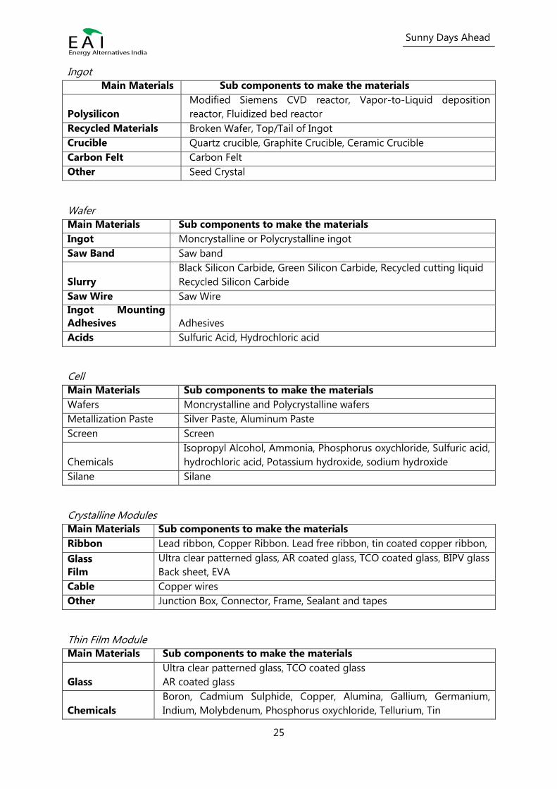
Raw Material, Machineries and Equipment for Core Products
Opportunities exist in manufacturing raw material and equipment for the following:
Ingots
Wafers
Cell
Modules
Raw Materials
A wide variety of raw materials and starting products are required for the entire solar PV
value chain. This section provides inputs on the key raw materials and starting products
required at each stage of the value chain. These inputs will provide the entrepreneurs
excellent insights into the types of opportunities that could be most suitable for them,
depending on their current line of business and their competencies.
In the tables below:
1) The LEFT HAND SIDE column indicates the MAIN MATERIALS required for
Manufacturing
2) The RIGHT HAND SIDE column indicates the sub components required for each
material
9 Source: Shurjo Energy (Company Website)
Sunny Days Ahead
25
Ingot
Main Materials Sub components to make the materials
Polysilicon
Modified Siemens CVD reactor, Vapor-to-Liquid deposition
reactor, Fluidized bed reactor
Recycled Materials Broken Wafer, Top/Tail of Ingot
Crucible Quartz crucible, Graphite Crucible, Ceramic Crucible
Carbon Felt Carbon Felt
Other Seed Crystal
Wafer
Main Materials Sub components to make the materials
Ingot Moncrystalline or Polycrystalline ingot
Saw Band Saw band
Slurry
Black Silicon Carbide, Green Silicon Carbide, Recycled cutting liquid
Recycled Silicon Carbide
Saw Wire Saw Wire
Ingot Mounting
Adhesives Adhesives
Acids Sulfuric Acid, Hydrochloric acid
Cell
Main Materials Sub components to make the materials
Wafers Moncrystalline and Polycrystalline wafers
Metallization Paste Silver Paste, Aluminum Paste
Screen Screen
Chemicals
Isopropyl Alcohol, Ammonia, Phosphorus oxychloride, Sulfuric acid,
hydrochloric acid, Potassium hydroxide, sodium hydroxide
Silane Silane
Crystalline Modules
Main Materials Sub components to make the materials
Ribbon Lead ribbon, Copper Ribbon. Lead free ribbon, tin coated copper ribbon,
Glass
Film
Ultra clear patterned glass, AR coated glass, TCO coated glass, BIPV glass
Back sheet, EVA
Cable Copper wires
Other Junction Box, Connector, Frame, Sealant and tapes
Thin Film Module
Main Materials Sub components to make the materials
Glass
Ultra clear patterned glass, TCO coated glass
AR coated glass
Chemicals
Boron, Cadmium Sulphide, Copper, Alumina, Gallium, Germanium,
Indium, Molybdenum, Phosphorus oxychloride, Tellurium, Tin
Sunny Days Ahead
26
TCO Material Diethyl Zinc
Oxides Zinc Oxide, Tin oxide
Acids Hydrochloric acid, Sulphuric acid
Other Junction Box, Connector, Cables, Frame, Sputtering Target
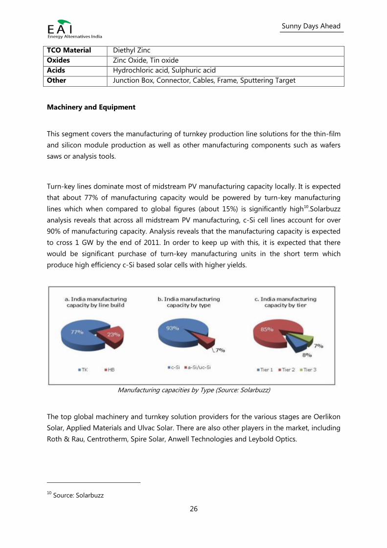
Machinery and Equipment
This segment covers the manufacturing of turnkey production line solutions for the thin-film
and silicon module production as well as other manufacturing components such as wafers
saws or analysis tools.
Turn-key lines dominate most of midstream PV manufacturing capacity locally. It is expected
that about 77% of manufacturing capacity would be powered by turn-key manufacturing
lines which when compared to global figures (about 15%) is significantly high10.Solarbuzz
analysis reveals that across all midstream PV manufacturing, c-Si cell lines account for over
90% of manufacturing capacity. Analysis reveals that the manufacturing capacity is expected
to cross 1 GW by the end of 2011. In order to keep up with this, it is expected that there
would be significant purchase of turn-key manufacturing units in the short term which
produce high efficiency c-Si based solar cells with higher yields.
Manufacturing capacities by Type (Source: Solarbuzz)
The top global machinery and turnkey solution providers for the various stages are Oerlikon
Solar, Applied Materials and Ulvac Solar. There are also other players in the market, including
Roth & Rau, Centrotherm, Spire Solar, Anwell Technologies and Leybold Optics.
10 Source: Solarbuzz
Sunny Days Ahead
27
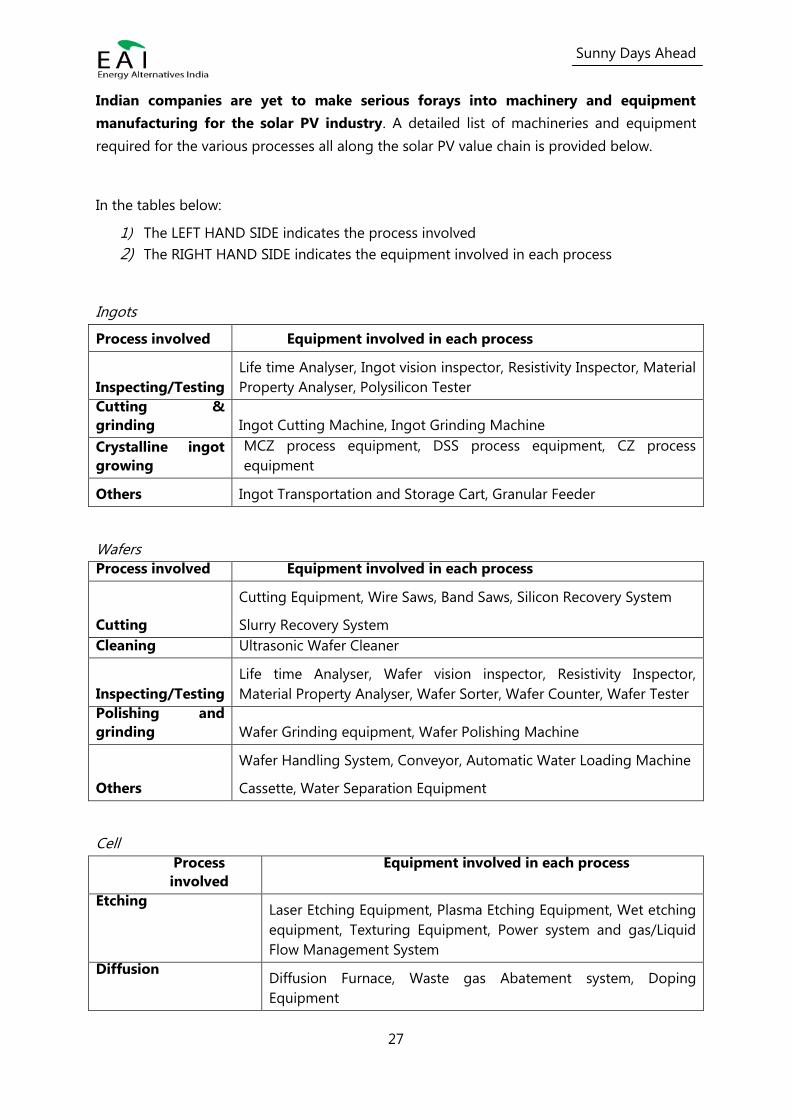
Indian companies are yet to make serious forays into machinery and equipment
manufacturing for the solar PV industry. A detailed list of machineries and equipment
required for the various processes all along the solar PV value chain is provided below.
In the tables below:
1) The LEFT HAND SIDE indicates the process involved
2) The RIGHT HAND SIDE indicates the equipment involved in each process
Ingots
Process involved Equipment involved in each process
Inspecting/Testing
Life time Analyser, Ingot vision inspector, Resistivity Inspector, Material
Property Analyser, Polysilicon Tester
Cutting &
grinding Ingot Cutting Machine, Ingot Grinding Machine
Crystalline ingot
growing
MCZ process equipment, DSS process equipment, CZ process
equipment
Others Ingot Transportation and Storage Cart, Granular Feeder
Wafers
Process involved Equipment involved in each process
Cutting
Cutting Equipment, Wire Saws, Band Saws, Silicon Recovery System
Slurry Recovery System
Cleaning Ultrasonic Wafer Cleaner
Inspecting/Testing
Life time Analyser, Wafer vision inspector, Resistivity Inspector,
Material Property Analyser, Wafer Sorter, Wafer Counter, Wafer Tester
Polishing and
grinding Wafer Grinding equipment, Wafer Polishing Machine
Others
Wafer Handling System, Conveyor, Automatic Water Loading Machine
Cassette, Water Separation Equipment
Cell
Process
involved
Equipment involved in each process
Etching Laser Etching Equipment, Plasma Etching Equipment, Wet etching
equipment, Texturing Equipment, Power system and gas/Liquid
Flow Management System
Diffusion Diffusion Furnace, Waste gas Abatement system, Doping
Equipment
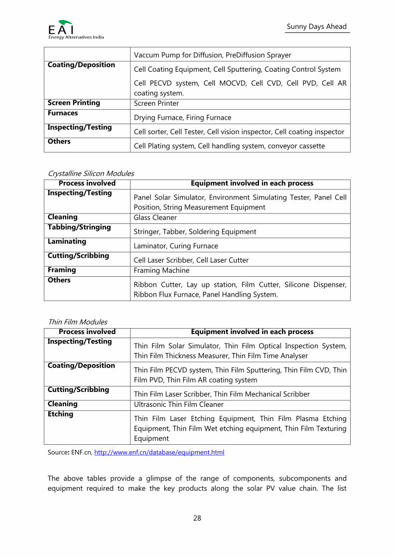
Sunny Days Ahead
28
Vaccum Pump for Diffusion, PreDiffusion Sprayer
Coating/Deposition Cell Coating Equipment, Cell Sputtering, Coating Control System
Cell PECVD system, Cell MOCVD, Cell CVD, Cell PVD, Cell AR
coating system.
Screen Printing Screen Printer
Furnaces Drying Furnace, Firing Furnace
Inspecting/Testing Cell sorter, Cell Tester, Cell vision inspector, Cell coating inspector
Others Cell Plating system, Cell handling system, conveyor cassette
Crystalline Silicon Modules
Process involved Equipment involved in each process
Inspecting/Testing Panel Solar Simulator, Environment Simulating Tester, Panel Cell
Position, String Measurement Equipment
Cleaning Glass Cleaner
Tabbing/Stringing Stringer, Tabber, Soldering Equipment
Laminating Laminator, Curing Furnace
Cutting/Scribbing Cell Laser Scribber, Cell Laser Cutter
Framing Framing Machine
Others Ribbon Cutter, Lay up station, Film Cutter, Silicone Dispenser,
Ribbon Flux Furnace, Panel Handling System.
Thin Film Modules
Process involved Equipment involved in each process
Inspecting/Testing Thin Film Solar Simulator, Thin Film Optical Inspection System,
Thin Film Thickness Measurer, Thin Film Time Analyser
Coating/Deposition Thin Film PECVD system, Thin Film Sputtering, Thin Film CVD, Thin
Film PVD, Thin Film AR coating system
Cutting/Scribbing Thin Film Laser Scribber, Thin Film Mechanical Scribber
Cleaning Ultrasonic Thin Film Cleaner
Etching Thin Film Laser Etching Equipment, Thin Film Plasma Etching
Equipment, Thin Film Wet etching equipment, Thin Film Texturing
Equipment
Source: ENF.cn, http://www.enf.cn/database/equipment.html
The above tables provide a glimpse of the range of components, subcomponents and
equipment required to make the key products along the solar PV value chain. The list
Sunny Days Ahead
29
provided is by no means exhaustive but is intended to make entrepreneurs acquainted with
the diverse opportunities.
Non-core Solar Products
In addition to the core business opportunities in manufacturing available along the solar PV
value chain, there are non-core opportunities for entrepreneurs and investors in this industry.
Some of the prominent non-core manufacturing opportunities are given below.
Solar Glasses
For crystalline cells, solar glass is used for protection and performance enhancement. In the
case of thin films, glass is used as a substrate.
Worldwide, in 2007, 138 million tons of glass was produced. Of this, 50 million tons were flat
glass, which is used in solar modules and reflectors. The flat glass market is worth €21 billion
annually but, only four companies namely NSG Group, AGC, Saint-Gobain and Guardian
Industries produce around 60% of the world's high quality float glass.
Few companies in India currently make glasses for solar cells, and Saint Gobain is one of
them; the Indian arm of the French glass giant is making serious efforts at extending its glass
products to cater to the demand of solar panels sector. Recently, Gujarat Borosil launched
solar grade glasses in Dec 2010.
Electrical Components: Inverters, Wires and Transformers
The manufacturing of inverters, charge controllers, wires and transformers is largely a
commodities business.
In the case of inverters, efficiencies of these devices are already relatively high, offering only
limited room for technical differentiation. There are exceptions - for instance, Steca Solar of
Germany provides a solution to the problem of partial shading when solar modules become
as inefficient as under full shading. The global leaders in inverters are SMA Solar
Technologies, Kaco and Fronius.
In India, the transformer and wires are sourced locally. Inverter manufacturers like Su-kam,
Luminous and Numeric are yet to fully start producing inverters for grid connected power
plants; hence, the inverters for MW scale solar PV power plants are mostly being imported.
Manufacturing Chemicals for Solar Industry
The manufacturing of photovoltaic modules, thermal receivers and reflectors requires a
number of chemicals and materials such as coatings, laminates, photovoltaic materials and
solar glass. Some of these chemicals have been listed above under Cells.
Sunny Days Ahead
30
Production of many of these chemicals also offers opportunities to Indian companies already
in the chemicals industry.
Central and State Policy Analysis
Central
The JNNSM has set an ambitious target of 20 GW of installed solar PV capacity in India by
2022. The policy aims to support this large scale of installation by fostering the growth of a
purpose built ecosystem which caters to every stage of the solar PV value chain. The
following sections discuss the implication of targets on the value chain.
Polysilicon
To sustain 20 GW worth of installations, India would require between 14,000 and
15,000 MT per year of polysilicon manufacturing capacity from the current non-
existent levels. As mentioned earlier, the main factor that determines the production output
of a polysilicon plant is the availability of uninterrupted power supply which poses a huge
challenge to the weak national grid with its heavy voltage fluctuations and generally poor
reliability (not to mention the high percentages of peak deficit in electricity supply that the
country is currently facing). The JNNSM document does not detail how this is to going to be
ensured.
Manufacturing plants need to be setup to produce polysilicon at large scales to remain cost
competitive (as cost of each stage in the value chain is propagated downstream and reflects
in the final module price). This translates to a high capital associated with the setting up of
manufacturing plants. Although the JNNSM document recommends low interest rate loans
and priority sector lending for manufacturing to achieve the installed capacity targets, they
would still be a far cry from what the global leaders (China) offer to their manufacturing
bases. The scale of investment required is unprecedented and the JNNSM scheme must
ensure that this is met.
Ingot/Wafer
It is estimated that by the end of the decade, the requirement for ingots/wafers would be
about 2000 MW. Production has to be scaled about 20 fold (from planned levels) to meet
this requirement.
As with polysilicon, ingots/wafers also require very large capital investment. Polysilicon cost
attributes to about 50% of the production cost. The lack of local supply means that this
cost of production becomes too large to sustain a profitable business. Thus incentives would
Sunny Days Ahead
31
have to be provided upstream to ensure growth. The incentives offered for ingot/wafer thus
is a function of the incentives offered for polysilicon, which has been discussed above.
Cells
Currently, a lack of a local ecosystem for the subcomponents required for solar cell
manufacture has stunted the growth of the sector in the country. Majority of the
components such as
Gases and chemicals used during the manufacturing process
Primary manufacturing equipment etc.
Have to be imported which results in a sharp increase in production costs. As with
polysilicon, the lack of uninterrupted power is also a source of major concern as the
manufacturing plants then would have to operate using backup power which further
increases the running cost of the plant.
Phase 1, Batch 2 of JNNSM stipulates that, for power plants using c-Si based modules, the
cells used would have to be locally manufactured. Although this is a positive step, it is
unsustainable as upstream components for cell manufacture would still have to be imported
which leads to a situation where locally manufactured cells/modules would not be cost
competitive with those available in the international market. With thin film modules not
having any domestic content requirement, the project developers would then prefer to go
for import of thin film modules thereby putting a dent on the local manufacturing
aspirations.
Modules
About 3000 MW per year module manufacturing capacity would be required by 2012 to
sustain the growth projected under JNNSM. With a current installed base of about 600 MW,
this target seems to be the one that is most achievable. Also, module manufacturing is
technically not a manufacturing process as such, but more of an assembly process which
adds to the ease of production.
As with cells, a stricter implementation of domestic content is required under JNNSM to
promote the local manufacture of modules.
Vertical Integration
The only way a local manufacturing system would be cost competitive is to ensure that all
manufacturing facilities are vertically integrated. JNNSM does not specifically promote
vertical integration of companies which, under current conditions is the most critical
Sunny Days Ahead
32
requirement. Thus the policy would have to promote vertical integration with specific
incentives for the same.
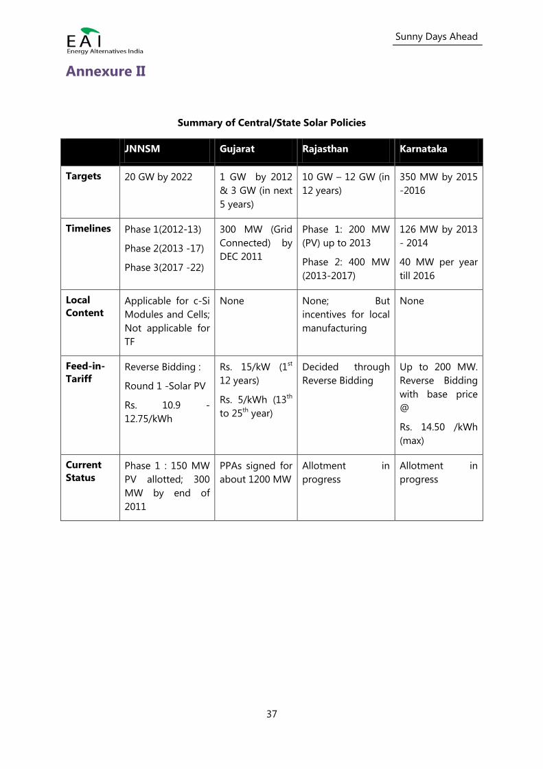
State Policy
As of September 2011, only 3 states have come up with a solar specific state policy – Gujarat,
Karnataka and Rajasthan. Of these only the Rajasthan state policy has clauses specifically
ensured to promote local manufacturing.
Under the Rajasthan policy, domestic manufacture is being promoted not by mandating
domestic content requirements, but by providing incentives for setting up of manufacturing
plants. The incentive provided is in the form of additional capacity allocation (of 200 MW) for
module manufacturers for setting up solar power plants.
The key point to be noted under the Rajasthan state policy is that it aims to promote
vertical integration. Incentives are provided only to those manufacturers who produce
modules, cells and wafers.Although this is a step in the right direction, the time frame
stipulated under the state scheme is far too short for proper implementation of a vertically
integrated line.
Sunny Days Ahead
33
Conclusion
In order for the costs of solar PV power to come down (so that it no longer remains a
policy driven industry), it is critical to build a complete ecosystem for solar PV rather than
just show significant growth at the tail end of the value chain (i.e. power production). This
implies that there is a genuine need for the creation of hundreds of companies along the
entire value chain - from polysilicon production to wafer to cell and module manufacturing,
as well as production of the supporting components. However, except for cells and
modules, there is hardly any manufacturing in India for the rest of the solar PV value
chain. There is thus a significant gap between what is needed and what is available.
The above facts have not been lost on the Indian government, which is coming up
with plans and incentives to facilitate the entry of many more Indian companies into the
manufacturing segment of the solar PV value chain. These efforts by the government to
build a complete solar PV ecosystem in India open up attractive opportunities for investors.
Compared to the PPA-bound power generation sector primarily driven by operational
efficiencies, the significantly higher potential for innovation in the manufacturing
sector also implies that companies could invest in building innovative and
differentiated businesses with significant upsides in future.
We foresee a future in which many Indian companies use their experience in the
manufacturing sector to participate in the manufacturing opportunities in the exciting solar
PV industry.
Sunny Days Ahead
34
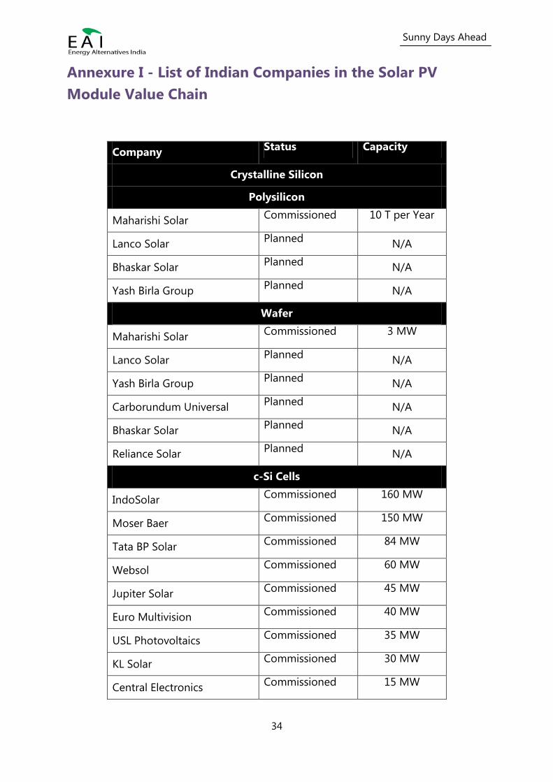
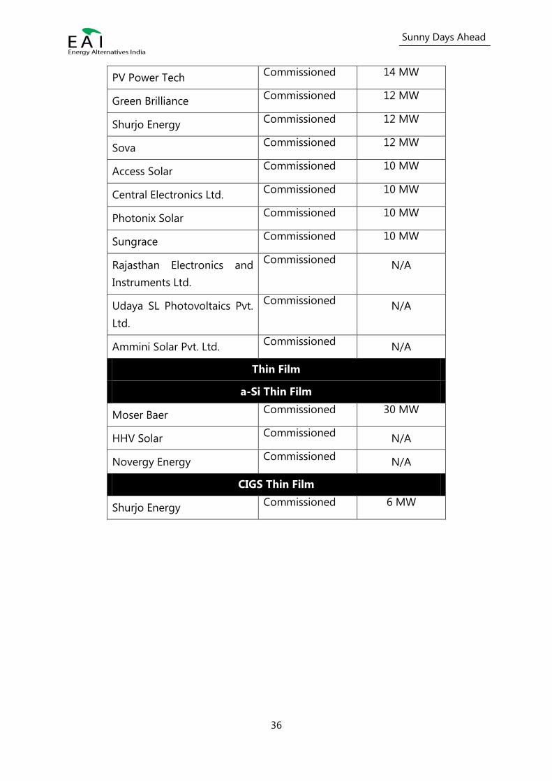
Annexure I - List of Indian Companies in the Solar PV
Module Value Chain
Company Status Capacity
Crystalline Silicon
Polysilicon
Maharishi Solar Commissioned 10 T per Year
Lanco Solar Planned
N/A
Bhaskar Solar Planned
N/A
Yash Birla Group Planned
N/A
Wafer
Maharishi Solar Commissioned 3 MW
Lanco Solar Planned
N/A
Yash Birla Group Planned
N/A
Carborundum Universal Planned
N/A
Bhaskar Solar Planned
N/A
Reliance Solar Planned
N/A
c-Si Cells
IndoSolar Commissioned 160 MW
Moser Baer Commissioned 150 MW
Tata BP Solar Commissioned 84 MW
Websol Commissioned 60 MW
Jupiter Solar Commissioned 45 MW
Euro Multivision Commissioned 40 MW
USL Photovoltaics Commissioned 35 MW
KL Solar Commissioned 30 MW
Central Electronics Commissioned 15 MW
Sunny Days Ahead
35
Shurjo Energy Commissioned 6 MW
Bharat Electronics Commissioned 5 MW
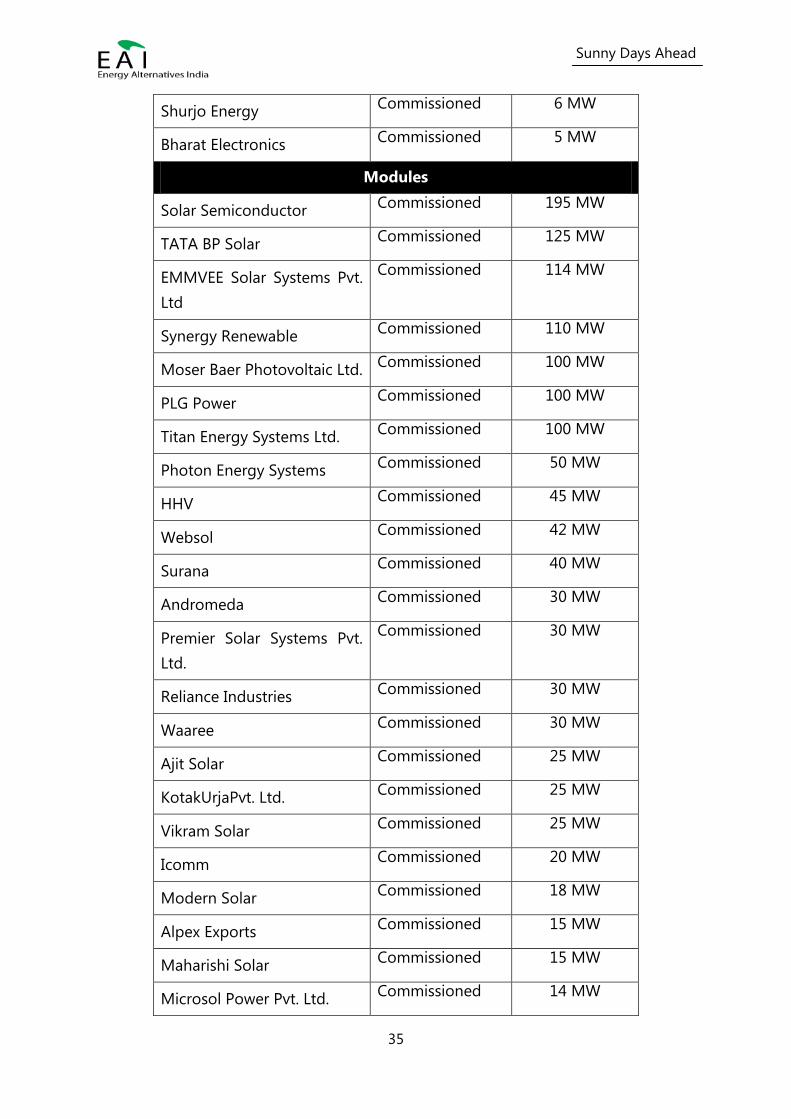
Modules
Solar Semiconductor Commissioned 195 MW
TATA BP Solar Commissioned 125 MW
EMMVEE Solar Systems Pvt.
Ltd
Commissioned 114 MW
Synergy Renewable Commissioned 110 MW
Moser Baer Photovoltaic Ltd. Commissioned 100 MW
PLG Power Commissioned 100 MW
Titan Energy Systems Ltd. Commissioned 100 MW
Photon Energy Systems Commissioned 50 MW
HHV Commissioned 45 MW
Websol Commissioned 42 MW
Surana Commissioned 40 MW
Andromeda Commissioned 30 MW
Premier Solar Systems Pvt.
Ltd.
Commissioned 30 MW
Reliance Industries Commissioned 30 MW
Waaree Commissioned 30 MW
Ajit Solar Commissioned 25 MW
KotakUrjaPvt. Ltd. Commissioned 25 MW
Vikram Solar Commissioned 25 MW
Icomm Commissioned 20 MW
Modern Solar Commissioned 18 MW
Alpex Exports Commissioned 15 MW
Maharishi Solar Commissioned 15 MW
Microsol Power Pvt. Ltd. Commissioned 14 MW
Sunny Days Ahead
36
PV Power Tech Commissioned 14 MW
Green Brilliance Commissioned 12 MW
Shurjo Energy Commissioned 12 MW
Sova Commissioned 12 MW
Access Solar Commissioned 10 MW
Central Electronics Ltd. Commissioned 10 MW
Photonix Solar Commissioned 10 MW
Sungrace Commissioned 10 MW
Rajasthan Electronics and
Instruments Ltd.
Commissioned N/A
Udaya SL Photovoltaics Pvt.
Ltd.
Commissioned N/A
Ammini Solar Pvt. Ltd. Commissioned
N/A
Thin Film
a-Si Thin Film
Moser Baer Commissioned 30 MW
HHV Solar Commissioned
N/A
Novergy Energy Commissioned
N/A
CIGS Thin Film
Shurjo Energy Commissioned 6 MW
Sunny Days Ahead
37
Annexure II
Summary of Central/State Solar Policies
JNNSM Gujarat Rajasthan Karnataka
Targets 20 GW by 2022 1 GW by 2012
& 3 GW (in next
5 years)
10 GW – 12 GW (in
12 years)
350 MW by 2015
-2016
Timelines Phase 1(2012-13)
Phase 2(2013 -17)
Phase 3(2017 -22)
300 MW (Grid
Connected) by
DEC 2011
Phase 1: 200 MW
(PV) up to 2013
Phase 2: 400 MW
(2013-2017)
126 MW by 2013
- 2014
40 MW per year
till 2016
Local
Content Applicable for c-Si
Modules and Cells;
Not applicable for
TF
None None; But
incentives for local
manufacturing
None
Feed-in-
Tariff Reverse Bidding :
Round 1 -Solar PV
Rs. 10.9 -
12.75/kWh
Rs. 15/kW (1st
12 years)
Rs. 5/kWh (13th
to 25th year)
Decided through
Reverse Bidding
Up to 200 MW.
Reverse Bidding
with base price
@
Rs. 14.50 /kWh
(max)
Current
Status Phase 1 : 150 MW
PV allotted; 300
MW by end of
2011
PPAs signed for
about 1200 MW
Allotment in
progress
Allotment in
progress
Sunny Days Ahead
38
Annexure III
SEMI Standards
The SEMI International Standards Program brings together industry experts to exchange
ideas and develop globally accepted technical standards for manufacturing. SEMI provides a
forum for the collaboration essential to move new and existing markets forward efficiently
and profitably.
The Economic Benefits of Standardization
• US National Institute of Standards and Technology (NIST) Study:
– Calibration, Standard Test Methods, and Software Standards resulted in
• $9.6 billion in benefits between 1996 and 2011
• Association Française de Normalisation (AFNOR) Study:
– Over 70% of companies participating in standardization reported that it
enabled them to anticipate future market requirements
• German Industry Study (DIN):
– Standards contribute more to economic growth than patents and licenses
• UK Department of Trade and Industry:
– Standards contribute £2.5 billion annually to economic growth in the UK
The Need for PV Standards
The solar PV industry needs to look at meaningful cost reduction through a global, robust
and well-organized supply chain. The current learning curve for the industry is not as steep
as other electronic industries, especially semiconductors which use many of the same
processes, materials, and suppliers as PV. A faster learning curve for the solar PV industry
could be accomplished through better industry collaboration, including industry standards
and technology roadmaps.
The progress made by semiconductors in cost reduction is one of the technological marvels
of our time. Since 1975, the cost of one transistor has been reduced by a factor of about
4,000,000. This achievement has often been ascribed to Moore’s Law, the prediction that
the number of transistors that can be placed inexpensively on an integrated circuit would
double approximately every two years. Many observers see Moore’s Law as a useful guide
to cost reduction in the PV industry. While thin film and c-Si cells do not benefit from
lithography-enabled feature-size reductions that comprise much of cost reductions in
semiconductors, much of Moore’s Law is directly related to productivity, yield, and other cost
Sunny Days Ahead
39
reductions not related to feature-size reductions. Since PV manufacturing is based upon
many of the same processes and materials as IC and display manufacturing, there remain
important learnings from these industries that can be applied to solar cells and modules.
• The PV industry currently has few standards to support the manufacturing process
and help achieve cost reduction and process efficiency goals
• The PV market, already large, is growing rapidly, with many new companies entering
the manufacturing supply chain
• Different applications and processes lead to diverse manufacturing challenges – this
is where industry standards can play a critical role by:
– Bringing the global supplier and customer communities together
– Collectively reducing the number of options in a given process
– Agreeing on common parameters and terminology
Why SEMI?
• Similarity between semiconductor, FPD and PV manufacturing – many SEMI
Standards are immediately applicable
• Well-established (35+years), transparent process for developing international
consensus manufacturing Standards
• Global infrastructure serving major PV manufacturing regions & over 500 volunteer
experts working in SEMI PV Standards Activities, led by PV industry veterans
Photovoltaic Standards at SEMI
Overview
For over 35 years, the SEMI International Standards Program has been well known for
developing global consensus standards for the semiconductor industry. Less well-known,
but now increasing in visibility, is the long SEMI history of developing PV Standards,
leveraging the many similarities that photovoltaic (PV) manufacturing has to that of the
semiconductor and FPD industries. The first SEMI Photovoltaic Standard, M6, Specification
for Silicon Wafers for Use as Photovoltaic Solar Cells, was published in 1981, now replaced
by SEMI PV22. With a global infrastructure serving major PV manufacturing regions, PV
Standardization activity at SEMI is now taking center stage.
Sunny Days Ahead
40
Photovoltaic Standards Committee
The first SEMI Standards Committee specifically dedicated to photovoltaics was formed in
2007, and rapidly developed SEMI PV1, a test method for solar-grade silicon feedstock, and
SEMI PV2, guide for PV equipment communication interfaces. There are now over 30 PV
Standardization activities underway at SEMI, both in crystalline silicon and thin film cell
technologies, and new PV Automation and PV Materials Committees have recently been
formed to specifically address standardization topics related to hardware and software
automation, materials and test methods.
Committees are now active in Europe, Japan, North America, and Taiwan, and a Working
Group is forming in China. Over 500 technical experts from leading companies in all
segments of the photovoltaic supply chain are currently involved in PV Standards efforts at
SEMI. Join them in this important effort.
Registration is free. Visit www.semi.org/standardsmembership.
Industry Participation is Critical
Momentum is building for the development and widespread adoption of standards in the
solar photovoltaic manufacturing industry. The SEMI Standards Program allows companies
to collaborate in a pre-competitive environment to define the best path to encourage
technical innovation and market growth. Companies that actively participate in the
development process stay current with industry technology trends, and more importantly,
these companies shape the development of the industry.
Published SEMI PV Standards
SEMI PV1 - Test Method for
MeasuringTrace Elements in Silicon
Feedstock for Silicon Solar Cells by High-
Mass Resolution Glow Discharge Mass
Spectrometry
• SEMI PV2 - Guide for PV Equipment
Communication Interfaces (PVECI)
• SEMI PV3 - Guide for High Purity Water
Used in Photovoltaic Cell Processing
• SEMI PV4 - Specification for Range of
5th Generation Substrate Sizes for Thin
Film Photovoltaic Applications
• SEMI PV5 - Guide for Oxygen (O2), Bulk,
Used In Photovoltaic Applications
• SEMI PV6 - Guide for Argon (Ar), Bulk,
Used In Photovoltaic Applications
• SEMI PV7 - Guide for Hydrogen (H2),
Bulk, Used In Photovoltaic Applications
• SEMI PV8 - Guide for Nitrogen (N2),
Bulk, Used In Photovoltaic Applications
• SEMI PV9 -Test Method For Excess
Charge Carrier Decay In PV Silicon
Materials By Non-Contact Measurements
Of Microwave Reflectance After A Short
Illumination Pulse
Sunny Days Ahead
41
• SEMI PV10 - Test Method For
Instrumental Neutron Activation Analysis
(INAA) Of Silicon
• SEMI PV11- Specifications for
Hydrofluoric Acid, Used In Photovoltaic
Applications
• SEMI PV12 - Specifications for
Phosphoric Acid, Used In Photovoltaic
Applications
• SEMI PV13 - Test Method for
Contactless Excess-Charge-Carrier
Recombination Lifetime Measurement in
Silicon Wafers, Ingots, and Bricks Using an
Eddy-Current Sensor
• SEMI PV14 - Guide For Phosphorus
Oxychloride, Used In Photovoltaic
Applications
• SEMI PV15 - Test Method for Measuring
BRDF Metrics to Monitor the Surface
Roughness and Texture of PV Materials
• SEMI PV16 - Specifications for Nitric
Acid, Used In Photovoltaic Applications
• SEMI PV17 - Specification for Virgin
Silicon Feedstock Materials for
Photovoltaic Applications
• SEMI PV18 - Guide for Specifying a
Photovoltaic Connector Ribbon
• SEMI PV19 - Guide for Testing
Photovoltaic Connector Ribbon
Characteristics
• SEMI PV20 - Specifications for
Hydrochloric Acid Used In Photovoltaic
Applications
• SEMI PV21 - Guide for Silane (SiH4),
Used In Photovoltaic Applications
• SEMI PV22 - Specification for Silicon
Wafers for Used in Photovoltaic Solar Cells
• SEMI PV23 - Test Method for
Mechanical Vibration of Crystalline Silicon
Photovoltaic (PV) Modules in Shipping
Environment
• SEMI PV24 - Guide for Ammonia (NH3)
In Cylinders, Used In Photovoltaic
Applications
• SEMI PV25 - Test Method for
Simultaneously Measuring Oxygen,
Carbon, Boron and Phosphorus in Solar
Silicon Wafers and Feedstock by
Secondary Ion Mass Spectrometry
• SEMI PV26 - Specifications for Hydrogen
Selenide (H2Se), Used In Photovoltaic
Applications
• SEMI PV27 - Specifications for
Ammonium Hydroxide (NH4OH), Used In
Photovoltaic Applications
Other SEMI Standards Applicable for PV Manufacturing
SEMI E10 - Specification for Definition and
Measurement of Equipment Reliability,
Availability, and Maintainability (RAM)
• SEMI F47 - Specification for
Semiconductor Processing Equipment
Voltage Sag Immunity
• SEMI M44 - Guide to Conversion Factors
for Interstitial Oxygen in Silicon
• SEMI MF1727 - Practice for Detection of
Oxidation Induced Defects in Polished
Silicon Wafer
Sunny Days Ahead
42
Current PV Standards Activities
• Analytical test methods
• Cell and module vibration test method
• Cell appearance and defect detection
• Cell specification template
•Equipment to equipment communication
• Minority carrier lifetime
• Process chemicals and gases
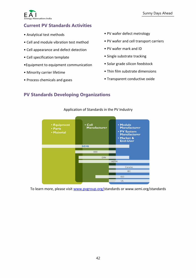
PV Standards Developing Organizations
Application of Standards in the PV Industry
To learn more, please visit www.pvgroup.org/standards or www.semi.org/standards
• PV wafer defect metrology
• PV wafer and cell transport carriers
• PV wafer mark and ID
• Single substrate tracking
• Solar grade silicon feedstock
• Thin film substrate dimensions
• Transparent conductive oxide
Sunny Days Ahead
43
EAI - Assisting Your Company for Attractive
Manufacturing Opportunities in Solar PV
EAI offers intelligence on the overall manufacturing opportunities in
Solar PV upstream – Polysilicon, Ingots and Wafers
Solar PV downstream – Cells and Modules
Thin Film manufacturing
Components – sub-components for cells and modules, chemicals and other
consumables
Balance of systems – inverters, monitoring systems
Equipment and machineries – Furnaces, wafer cutting tools, cell production line,
module production line
Identifying the most attractive opportunities for your company
Understanding your company’s aspirations in the context of solar energy sector
Understanding your company’s manufacturing competencies
Evaluating the fit between your aspirations + competencies and the available
opportunities
Clearly identifying the attractive opportunities appropriate for your company
Feasibility study for shortlisted opportunities
Demand and supply analysis
Costs and returns estimates
Strategic dimensions – extent of competition, buyer and supplier power, dominant
designs and industry concentration, degree of innovation, barriers to entry
Possibilities of JVs and technology partnerships
Identification of key success factors
Key characteristics of each opportunity
Sunny Days Ahead
44
Strengths
Dedicated Focus on Renewables - We work only in renewable energy and nothing
else.
Wide Expert Network - We work with over 100 technical and business experts across
all primary renewable energy sources.
Financial Assistance - We work with over 25 different PE, VC firms and banks
providing our client easy access to finance.
Clients
EAI's consulting team has been assisting several organizations in diverse renewable energy
domains. Some of our esteemed clients include:
PepsiCo
Reliance Industries
World Bank
Sterlite Technologies
Bill & Melinda Gates Foundation
iPLON GmbH
Minda Group
GE
Bhavik Energy
Agarwal Group
Prominent companies that have benefitted from our research and reports:
Accenture
AT Kearney
Shell
Lafarge
Exxon Mobil
Boston Consulting Group
Schneider Electric
Bosch
GE
Danfoss Solar
IFC
Siemens
Sharp
Gehrlicher Solar AG
Reliance Solar
Emergent Ventures
Videocon
Q Cells
Emerson Network Power
Indian Railways
Sunny Days Ahead
45
EAI’s Replacing Diesel with Solar
Looking to save on diesel by moving to captive solar power? EAI’s Replacing Diesel with
Solar report is a one-stop resource for all the information you will need to assess, implement,
and profit from substituting diesel with solar. Within this report you will find
• Captive solar PV technology and components
• Constraints in replacing diesel with solar
• Government incentives and regulations
• Inputs on capital and operational costs and financial scenario analysis
• Case studies for those businesses that already use solar for captive power
• Financing options
• Vendors, component suppliers, and system integrators
• List of solar PV captive power plant systems all over India
Please click here for detailed contents, critical questions answered, and a free preview of the
report.

Sunny Days Ahead
46
Sunny Days Ahead
47
About SEMI and PV Group
SEMI is the global industry association serving the manufacturing supply chains for the
micro- electronic, display and photovoltaic industries.
PV Group represents SEMI member companies
involved in the solar energy manufacturing supply
chain. Members provide the essential equipment,
materials and services necessary to produce clean,
renewable energy from photovoltaic technologies.
The PV Group mission is to advance industry growth,
support continuous efficiency improvements and
promote sustainable business practices through
international standards development, events, public
policy advocacy, EHS support, market intelligence,
and other services
SEMI India, the Indian arm of SEMI, was established in late 2008 to promote the growth and
development of the solar/PV and adjacent industries
Vision
SEMI promotes the development of the global semiconductor, display, MEMS,
Photovoltaic and related industries and positively influences the growth and prosperity of
its members. SEMI advances the mutual business interests of its membership and promotes
fair competition in an open global marketplace
Mission
SEMI will provide enlightened industry stewardship and effectively engage the imagination,
creative energy and commitment of our members and employees to advance the welfare of
the global semiconductor, display, MEMS, Photovoltaic and related industries
SEMI will:
• Create recognized platforms for industry networking and collaboration
• Promote accurate and efficient communication and information exchange
• Support initiatives that positively influence our global industry and environment
• Foster a global continuous process improvement culture that drives strategic
decision making and speed of execution
Sunny Days Ahead
48
About SOLARCON India
SOLARCON India is the premier annual solar technology and business event organized by
SEMI PV Group, in the region, and combines an International class Industry exposition with
conferences and technical workshops/short courses.
SOLARCON India is part of the global calendar of SEMI events, and debuted at the
Hyderabad International Convention Centre (HICC) in 2009 and establishing itself as the
platform of choice to showcase products, solutions and capabilities, meet and network with
buyers, suppliers, members of the solar community and to understand the latest technology
trends and opportunities in the solar business. It is supported by the SEMI India PV Advisory
Committee comprising leading executives from across many segments of the solar industry
in India.
SOLARCON India shows have been supported by the Ministry of New & Renewable Energy,
IREDA, agencies of the Government of Andhra Pradesh and have attracted leading global
solar and photovoltaics experts as speakers.
November 9-11, HICC, Hyderabad
Supported by
Ministry of New & Renewable Energy Government of India
Trade Fair Certification by