sunplus camera solution - open ip camera forum sheets/spca-533a.pdfdigital still camera controller...
TRANSCRIPT

DIGITAL STILL CAMERA CONTROLLER
SUNPLUS TECHNOLOGY CO. reserves the right to change this documentation without prior notice. Information provided by SUNPLUS TECHNOLOGY CO.
is believed to be accurate and reliable. However, SUNPLUS TECHNOLOGY CO. makes no warranty for any errors which may appear in this document.
Contact SUNPLUS TECHNOLOGY CO. to obtain the latest version of device specifications before placing your order. No responsibility is assumed by
SUNPLUS TECHNOLOGY CO. for any infringement of patent or other rights of third parties which may result from its use. In addition, SUNPLUS products
are not authorized for use as critical components in life support devices/ systems or aviation devices/systems, where a malfunction or failure of the product
may reasonably be expected to result in significant injury to the user, without the express written approval of Sunplus.
PAGE 1
SPCA533AUser Guide
Preliminary
SSuunnpplluuss CCaammeerraa SSoolluuttiioonn
SSPPCCAA553333AAUser Guide
Version 0.2.0
June 14, 2002
is a trade mark of Sunplus.
SPCA533A
© Sunplus Technology Co., Ltd.
Proprietary & Confidential
PAGE 2 Jun. 14, 2001
Preliminary Version: 0.2.0
Preliminary User Guide
Contents
1. OPERATIONAL DESCRIPTIONS ................................................................................................................................ 5
1.1 OPERATION MODES......................................................................................................................................................... 51.1.1 Preview mode .......................................................................................................................................................... 51.1.2 Capture mode .......................................................................................................................................................... 51.1.3 Continuous shot ....................................................................................................................................................... 61.1.4 Video Clip ................................................................................................................................................................ 61.1.5 Playback .................................................................................................................................................................. 7
1.2 GLOBAL.......................................................................................................................................................................... 71.2.1 Clocks ...................................................................................................................................................................... 71.2.2 Power On Sequence............................................................................................................................................... 101.2.3 Suspend/resume control ......................................................................................................................................... 11Sensor interface.............................................................................................................................................................. 12RTC................................................................................................................................................................................. 13USB interface ................................................................................................................................................................. 131.2.4 Power Saving Consideration ................................................................................................................................. 141.2.5 User Interface........................................................................................................................................................ 151.2.6 Global Timer Control ............................................................................................................................................ 171.2.7 RTC........................................................................................................................................................................ 181.2.8 Pattern Generator ................................................................................................................................................. 201.2.9 Interrupt Events ..................................................................................................................................................... 22
1.3 CDSP ........................................................................................................................................................................... 231.3.1 Image size limitation.............................................................................................................................................. 231.3.2 Horizontal Mirror on Raw Data............................................................................................................................ 261.3.3 Horizontal Scale Down on Raw Data.................................................................................................................... 281.3.4 Hardwired Color Processor................................................................................................................................... 28
1.4 DMA CONTROLLER...................................................................................................................................................... 331.4.1 Direction of the DMA ............................................................................................................................................ 331.4.2 Page size adjustment of the DMA.......................................................................................................................... 351.4.3 Matching pattern in DMA...................................................................................................................................... 351.4.4 DMA control flow .................................................................................................................................................. 37
1.5 STORAGE MEDIA........................................................................................................................................................... 391.5.1 PIO mode and DMA mode..................................................................................................................................... 401.5.2 Nand-gate flash memory and SmartMediaCard .................................................................................................... 401.5.3 CompactFlash cards interface............................................................................................................................... 421.5.4 SPI interface to the Serial flash memory ............................................................................................................... 431.5.5 Next flash serial interface control ......................................................................................................................... 441.5.6 SD memory cards interface ................................................................................................................................... 451.5.7 The ECC generation .............................................................................................................................................. 49
1.6 JPEG ENGINE ............................................................................................................................................................... 501.6.1 Quantization table ................................................................................................................................................. 501.6.2 JPEG compression ................................................................................................................................................ 511.6.3 JPEG decompression............................................................................................................................................. 53
1.7 USB BUS INTERFACE .................................................................................................................................................... 561.7.1 USB Vendor Command .......................................................................................................................................... 561.7.2 USB Packet Format............................................................................................................................................... 60
1.7.2.1 USB Video Iso-in Packet (endpoint 1) ................................................................................................................................601.7.2.2 USB BULK-IN Packet (endpoint 2, 7) ................................................................................................................................611.7.2.3 USB BULK-OUT Packet (endpoint 3, 8) ............................................................................................................................611.7.2.4 USB Interrupt-IN Packet (endpoint 4, 9).............................................................................................................................611.7.2.5 Audio INTERRUPT-IN pipe (endpoint 5) ..........................................................................................................................61

SPCA533A
© Sunplus Technology Co., Ltd.
Proprietary & Confidential
PAGE 3 Jun. 14, 2001
Preliminary Version: 0.2.0
Preliminary User Guide
1.7.2.6 Audio ISO-IN Pipe (endpoint 6)..........................................................................................................................................611.7.3 Bulk-Only Protocol Support .................................................................................................................................. 621.7.4 Waking up the camera by the USB plug in/out ...................................................................................................... 64
1.8 AUDIO FUNCTION ......................................................................................................................................................... 641.8.1 AC ‘97 Controller .................................................................................................................................................. 651.8.2 Codec Controller ................................................................................................................................................... 651.8.3 Down-sampling Filter ........................................................................................................................................... 661.8.4 ADPCM Codec ...................................................................................................................................................... 661.8.5 Audio Buffer Controller......................................................................................................................................... 661.8.6 MP3 Processor Interface....................................................................................................................................... 691.8.7 Programming flow of the MP3 processor serial interface..................................................................................... 70
1.9 SDRAM CONTROLLER ................................................................................................................................................. 711.9.1 SDRAM initialization............................................................................................................................................. 711.9.2 SDRAM refresh...................................................................................................................................................... 711.9.3 CPU access SDRAM.............................................................................................................................................. 721.9.4 Filling constant data to the SDRAM...................................................................................................................... 731.9.5 Interface with DMA controller .............................................................................................................................. 731.9.6 Image data input control ....................................................................................................................................... 731.9.7 Data format ........................................................................................................................................................... 741.9.8 JPEG interface ...................................................................................................................................................... 751.9.9 Thumbnail generation ........................................................................................................................................... 751.9.10 Image-Processing engine..................................................................................................................................... 76
1.9.10.1 Image-scaling operation ....................................................................................................................................................761.9.10.2 Image rotation operation....................................................................................................................................................781.9.10.3 Copy & paste operation .....................................................................................................................................................791.9.10.4 Date stamping operation....................................................................................................................................................801.9.10.5 DRAM-to-DRAM DMA operation ...................................................................................................................................811.9.10.6 Bad-Pixel correction..........................................................................................................................................................831.9.10.7 Inter-frame raw data subtraction operation........................................................................................................................841.9.10.8 YUV420-to-YUV422 conversion......................................................................................................................................85
1.9.11 SDRAM space partition in different operation mode........................................................................................... 861.10 SERIAL INTERFACE...................................................................................................................................................... 93
1.10.1 Synchronous Serial interface (SSC)..................................................................................................................... 931.10.2 Three-wire interface ............................................................................................................................................ 961.10.3 Manual control of the serial interface ................................................................................................................. 98
1.11 TV-IN / CMOS SENSOR INTERFACE .......................................................................................................................... 991.11.1 TV input interface ................................................................................................................................................ 991.11.2 CMOS interface ................................................................................................................................................. 102
1.11.2.1 I/O direction for sensor interface ..................................................................................................................................... 1021.11.2.2 Clock system for sensor interface .................................................................................................................................... 1021.11.2.3 Hsync, Vsync output signal generate:.............................................................................................................................. 1041.11.2.4 Hsync, Vsync Reshape .................................................................................................................................................... 1051.11.2.5 Hvalid, Vvalid generation................................................................................................................................................ 105
1.11.3 Image Capture: .................................................................................................................................................. 1061.11.4 Flash light control for CMOS sensor................................................................................................................. 107
1.11 CCD INTERFACE....................................................................................................................................................... 1081.12.1 Operation modes: .............................................................................................................................................. 1081.12.2 Electronic shutter control .................................................................................................................................. 1101.12.3 Mechanical shutter control.................................................................................................................................1111.12.4 Flash light control for the CCD sensor ............................................................................................................. 1121.12.5 Image capture .................................................................................................................................................... 116
1.13 EMBEDDED MICRO-CONTROLLER ............................................................................................................................. 1171.13.1 Hardware interface............................................................................................................................................ 1171.13.2 RAM space......................................................................................................................................................... 119

SPCA533A
© Sunplus Technology Co., Ltd.
Proprietary & Confidential
PAGE 4 Jun. 14, 2001
Preliminary Version: 0.2.0
Preliminary User Guide
1.13.3 ROM space ........................................................................................................................................................ 1201.13.4 ISP (In-system-programming) ........................................................................................................................... 1211.13.5 The difference between the standard 8032 and the embedded 8032.................................................................. 1221.13.6 Suspend state power control of CPU................................................................................................................. 122
1.14 TV OUTPUT INTERFACE ............................................................................................................................................ 1231.14.1 Analog TV interface (tvdspmode=0~1, register 0X2D00)................................................................................. 1231.14.2 Digital TV interface........................................................................................................................................... 123
5.14.2.1 CCIR 656 interface (dspmode=2~3, register 0X2D00) ................................................................................................... 1235.14.2.2 CCIR 601 interface (tvdspmode=4~7, register 0X2D00) ................................................................................................ 1241.14.2.3 Unipac UPS051 (TFT-LCD interface, dspmode=8, register 0X2D00)............................................................................ 1241.14.2.4 EPSON D-TFD LCD interface (tvdspmode=10, register 0X2D00) ................................................................................ 1241.14.2.5 CASIO TFD LCD interface (tvdspmode=11, register 0X2D00) ..................................................................................... 1241.14.2.6 GIANTPLUS STN-LCD interface (tvdspmode=12, register 0X2D00)........................................................................... 1241.14.2.7 PRIME VIEW TFT-LCD interface (tvdspmode=14, register 0X2D00).......................................................................... 1251.14.2.8 User define output interface (tvdspmode=15, register 0X2D00) ..................................................................................... 1251.14.2.9 Horizontal and Vertical Timing and Corresponding Register .......................................................................................... 125
1.14.3 On Screen Display (OSD).................................................................................................................................. 1281.14.3.1 Font-Based OSD.............................................................................................................................................................. 1291.14.3.2 graphic-based OSD.......................................................................................................................................................... 131
1.14.4 Gamma correction............................................................................................................................................. 1311.14.4 vertical and horizontal scaling function ............................................................................................................ 132
2. REGISTER DESCRIPTIONS..................................................................................................................................... 133
2.1 REGISTER CATEGORY ................................................................................................................................................. 1332.2 GLOBAL REGISTERS ................................................................................................................................................... 1332.3 CDSP REGISTERS....................................................................................................................................................... 1412.4 CDSP WINDOW REGISTERS ....................................................................................................................................... 1462.5 DMA CONTROLLER REGISTERS ................................................................................................................................. 1492.6 FLASH MEMORY CONTROL REGISTERS ...................................................................................................................... 1512.7 USB CONTROL REGISTERS......................................................................................................................................... 1572.8 AUDIO CONTROL REGISTERS...................................................................................................................................... 1622.9 SDRAM CONTROL REGISTERS .................................................................................................................................. 1652.10 JPEG CONTROL REGISTERS ..................................................................................................................................... 1732.11 SERIAL INTERFACE CONTROL REGISTERS................................................................................................................. 1742.12 TV-IN / CMOS SENSOR CONTROL REGISTER .......................................................................................................... 1772.13 CCD CONTROL REGISTERS ...................................................................................................................................... 1802.14 CPU CONTROL REGISTERS....................................................................................................................................... 1822.15 TV OUTPUT INTERFACE REGISTERS ......................................................................................................................... 183
3. APPLICATION/USAGE DESCRIPTIONS (BY FAE) ............................................................................................. 189
REVISION HISTORY ..................................................................................................................................................... 190

SPCA533A
© Sunplus Technology Co., Ltd.
Proprietary & Confidential
PAGE 5 Jun. 14, 2001
Preliminary Version: 0.2.0
Preliminary User Guide
1. Operational Descriptions
1.1 Operation modes
The main operation modes of the SPCA533A are preview, capture, videoclip and playback modes. These modes are mutually exclusive.
The SPCA533A can only operated in one of these modes at a time. There are many tasks that can be excuted concurrently with these
modes. For example, data transfer between the PC and the camera can take place while the camera is in any of these operation modes.
Also, data transfer between the camera and the storage media can also be performed while the SPCA533A is operated in any operation
modes. These concurrence operations are useful when the application need to put the time-consuming tasks to the background execution.
1.1.1 Preview mode
In the preview mode, the SPCA533A receives raw image data from the sensor. It processes the data in real time with the CDSP (Color
DSP) and stores the data in the frame buffer of the SDRAM. Then, the data is read from the SDRAM and sent to the display device. The
SPCA533A supports TFT LCD panels, STN LCD panels, digital TV output and analog TV output. The following diagram demonstrates the
data flow in the preview mode.
SensorsRGB raw data inBayer format
DSPYUV422
interleave format
Sensors in monitor ordecimation mode
1. Horizontal-scaling2. Color processing3. RGB-toYUV conversion
SDRAMLCD interface controller
YUV422interleave format
external frame buffer
1. Scaling to fit the resolution of the display devices2. output to TV or LCD
The sensor’s fame rate are normally adjusted to 30 fps in the preview mode. For the CCD sensors, the user need to adjust the
parameters in the built-in timing generator to make the SPCA533A drive out 30 fps timing. For the CMOS sensors, the frame rate may be
dominated by the SPCA533A or by the sensors, depending on the operation mode of the CMOS sensors. If the CMOS sensors is operated
in the master mode, the SPCA533A programs the internal registers of the sensors to control the timing. On the other hand, if CMOS sensors
is operated is operated in the slave mode, the users need to adjust the parameters in the CMOS interface controller of the SPCA533A to
control the frame rate. Mega-pixel sensors usually supports monitor mode (CCD) or decimation mode (CMOS) to allow the pixel data to be
read at 30 fps frame rate.
The SPCA533A provides many programmable parameters in the CDSP to achieve the best image quality. The image is horizontally
scaled-down by the CDSP, too. The horizontal scaling-down function in the DSP not only reduces the bandwidth requirement of the SDRAM
but also maintain the appropriate aspect ratio of the image in a CCD system. For example, if the a CCD sensor vertically subsampled the
image by 4, then the CDSP will need to scale down the image horizontally by 4 to maintain the correct aspect ratio. After color processing,
the CDSP convert the image data from the RGB domain to the YUV domain. The AE (auto-exposure) and AWB (auto-white balance
firmware) algorithm is executed at the background in the preview mode. The CDSP provides statistics on the image data for the AE/AWB
algorithm’s reference.
The data stored in the SDRAM is in YUV422 format. The SDRAM controller maintains two frame buffers to convert the frame rate if the
sensor’s frame rate is different from the frame rate of the display device.
To fit a wide range of the resolutions of the display devices, The LCD/TV interface controller has built-in scaling function. The scaling
ratio of the LCD/TV scaling function can be adjusted independently in the vertical direction and the horizontal direction. However, it is
important to maintain the appropriate aspect ratio of the original image. For TV output, the PAL frame rate fixed at 25 fps, the NTSC is 30fps.
The frame rates of the LCD panels are usually fiexed by the panel makers.
1.1.2 Capture mode
The capture mode allows the user to capture image output from the sensors. Depending on the setting of the camera, the SPCA533A is
able to capture a single image, multiple images and video. The simplest flow is the single image capture. The following diagram shows the
data flow of snapping a single image.

SPCA533A
© Sunplus Technology Co., Ltd.
Proprietary & Confidential
PAGE 6 Jun. 14, 2001
Preliminary Version: 0.2.0
Preliminary User Guide
SensorsRGB raw data inBayer format
SDRAM
Sensors in monitor ordecimation mode
Bad pixel concealment
DCSP SDRAMYUV422
interleave format
1.Scaling2.compression3.DCF/EXIF file construction
RGB raw data inBayer format
Storage media
1. Color processing2. RGB-toYUV conversion
LCD/TV
DMA
In the capture mode, the sensor should be operated in the full resolution mode. This requires adjusting the parameters in the timing
generator in the CCD system. In the CMOS system, the sensor’s control registers must be adjusted accordingly.
The RGB raw data (in Bayer pattern format) is stored in the SDRAM frame buffer without any image processing. Only optical black value
is measured when the data is written into the SDRAM. For interlace CCD sensors, the data sequnce of the image data is re-arranged at the
same time when the raw data is written into the SDRAM. This is necessary because the this type of sensors separate the image into R-field
and B-field. Also, 12 extra lines must be captured. This is necessary for the color processing in the SPCA533. For example, to get a 1280 by
960 final image, the users must capture a 1296 by 972 image first. Some sensors might not have enough number of valid pixels to meet the
requirement of the SPCA533’s color processing. An altenative approach is to mirror the image at the boundaries of the incoming data.
Please reference to the CDSP section for details. The bad pixel concealment can be done in the SDRAM before color processing. The
coordinates of the bad pixles are usually stored in the external ROM. The SPCA533A has built-in a hardwired engine for the bad pixel
concealment to speed up this step.
After bad pixel concealment, the data is sent to the CDSP for color processing. In the color processing, the optical black value measure
in the previous step is used. The color processing can be done many times with different parameter setting of the CDSP. This is useful when
the flash light is applied to the image in which the preview mode AE/AWB window statistics cannot be used in the image precessing.
After the image processing, the image is converted into YUV422 format and stored in the SDRAM again. The YUV422 image may be
optionally scaled to the desired size. This step is necessary when the image is digitally zoomed or when a lowe resolution image is required.
The scale function can be used to generate the thumbnail data, too. If a quick-view of the snapped image is requires, the YUV422 image
should be scaled to fit the resolution of the display device before viewing. Image compression and file format (EXIF2.1 , DCF) construction
are also done in the SDRAM. The SPCA533’s JPEG engine process only the VLC stream. If the users intend to generate the DCF/EXIF file,
the header must be generated and combined in the SDRAM. The files is then saved to the storage media via the SPCA533’s built-in DMA
controller. The file saing can be execured in the background, meaning the SPCA533A may switch back to the preview mode before the file is
not completed written to the storage media.
1.1.3 Continuous shot
The continuous shot is also supported by the SPCA533. To minimize the time interval between frame, the multiple raw images are
stored in the SDRAM before any processing. The size of the SDRAM determines the maximum number of the raw images in the continuous
shot. The maximum frame rate in the continuous shot is the maximum frame rate of the sensors. After the required raw images are captured,
they are process one by one. The precessing includes bad pixel concealment, all the color processing, scaling, compression, and file saving.
It is exactly the same as snapping a single image.
In the CCD system, there is usually an exposure frame between data dumping frames. In the exposure frame, no data is read out from
the sensos. This exposure frame can be used to perform CDSP color processing. In this case, the overall performace of the continuous shot
will be improved. Also the images after CDSP color processing can be sent to the display device. The SPCA533’s LCD/TV controller can
only display the iamge in YUV422 format. RGB data can not be viewed.
There are many possibilities for the display in the continuous shot. The snapped image can be shown one by one on the LCD(or TV)
after they are captured. Alternatively, the thumbnails can be shown together. This is up to the system application.
1.1.4 Video Clip
The video capture function operates similar to the preview mode, except that the data in the SDRAM is sent to the JPEG engine for
compression and tehn stored in the storage media. The bandwidth requirement in the videoclip is the highest among all the operations of the
SPCA533. To construct a video file of the AVI format, the firmware must maintain the header of the AVI. The following diagram shows the
data flow of the videoclip.

SPCA533A
© Sunplus Technology Co., Ltd.
Proprietary & Confidential
PAGE 7 Jun. 14, 2001
Preliminary Version: 0.2.0
Preliminary User Guide
SensorsRGB raw data inBayer format
DSPYUV422
interleave format
Sensors in monitor ordecimation mode
1. Horizontal-scaling2. Color processing3. RGB-toYUV conversion
SDRAM
LCD interface controller
YUV422interleave format
DMAStorage media
JPEG
1.1.5 Playback
In the playback mode, the SPCA533A fetches the compressed image in the storage media. The headers of the image files are parsed by
the firmware. The JPEG quantization table must be programmed before decompression starts. The decomressed image is written into the
display buffer for viewing. For mega-pixel sensors, the image normally needs to be scaled dwon before sending to the display devices
because the resolution of the display device is smaller than the resolution of the images. The SPCA533A can display multiple images at the
same time, too. When this feature is to be implemented, thumbnail images can be used to speedup the playback. Aslo the copy&past engine
in the DRAM controller can help the firmware to construct the image in the display buffer. The LCD/TV interface controller can only display
YUV422 image. If the original file is in YUV420 format, it must be converted to YUV422 format beore viewing. The following diagram is the
data flow in the playback mode.
Storage mediaDCF/EXIF files
SDRAM YUV422/420
1. parse the header2. fill the Q table3. decompress
SDRAMLCD interface controller
YUV422interleave format
1. scaling2. paste to the display buffer3. convert to YUV422 if necessary
Decompressing a full-size image may take some time, depending on the image resolution. The bottoleneck is often located in the access
speed of the storage media. Another approach in the playback mode is to decompress and display the thumbnail image first (resolution 160
by 120). The decompression of the full-size image can be done in the background while the users are viewing the thumnails. Displaying
the thumbnail image requires the LCD/TV interface to scale up the image. This can be done by adjusting the scale factors of the LCD/TV
interface controller. Once the full size image is decompressed and scaled to the appropriate size, the firmware may switch the display buffer
to display the image of better quality.
1.2 Global
1.2.1 Clocks
The SPCA533A connects to three external crystals. The first one (RTC crystal) is 32.768KHz, which is used in the built-in RTC module.
This crystal could be spared when the RTC module is not used. The second crystal (TV crystal) is 27 MHz. This crystal is necessary when
the SPCA533’s built-in video CODEC is used. The third crystal (USB crystal) is to provide the main operating frequency of the SPCA533.
The main operating frequency is generated by the main phase lock loop (MPLL). The input clock frequency of the MPLL could be 6MHz,
12MHz, or 24 MHz, depending on the IO-trap values. To reduce the counts of the external components, the SPCA533’s MPLL can also take
the 27MHz clock as its input source. This configuration is selected by a dedicated input pin. The following table lists the main clock settings.
Onextal
Pin-B13(280), pin-134(216)IO-trap{4:3} USB crystal TV crystal
0 0 6MHz NC
0 1 12MHz NC
0 2 24MHz NC
0 3 48MHz NC
1 Don’t care NC 27MHz
Note when 48MHz USB crystal is used, the main internal phase lock loop will be disabled to reference the external clock directly.

SPCA533A
© Sunplus Technology Co., Ltd.
Proprietary & Confidential
PAGE 8 Jun. 14, 2001
Preliminary Version: 0.2.0
Preliminary User Guide
The clock supply to the CMOS sensors and to the internal timing generator (for the CCD systems) is a critical factor in the determination
the frame rate and exposure time. The SPCA533A can supply this clock by the main phase lock loop (MPLL). Alternatively, the SPCA533A
can supply this clock by a dedicated phase lock loop(TGPLL). The clock source is chosen based on the pixel clock of the sensors. If the pixel
clock is 12MHz, choice the MPLL and disable the TGPLL to conserve power. If the pixel clock of the sensors is 18MHz, choose the TGPLL
to supply the clock. The TGPLL can also outputs other frequencies such as 21MHz, it is controlled by the input parameters of the TGPLL.
The output clock frequency of the TGPLL is 3MHz*(TGPLLNS1+1)*(TGPLLNS2+1)/(TGPLLS+1)*2
TGPLLS TGPLLNS1 TGPLLNS2 TGPLL
0 3 5 144 MHz
0 3 6 168 MHz
The 8XCK (8X pixel clock) is the input clock of the timing generator, which could be selected by the following setting.
TVDecMode (register 0X2018[0]) TGPllEn (register 0X2080[0]) 8XCK
1 Don’t care 27 MHz
0 0 96 MHz
0 1 TGPLL output
The 2XCK (2X pixel clock) is selected by the following setting.
Extclk2xdiv (register 0X2A82[7:0]) 2XCK
0 8XCK / 1
1 8XCK / 2
2 8XCK / 3
… …
254 8XCK / 255
255 8XCK / 256
The 1XCK (pixel clock) is selected by the following setting.
Extclk1xdiv (register 0X2A81[3:0]) 1XCK (pixel clock)
0 2XCK / 1
1 2XCK / 2
2 2XCK / 3
… …
15 2XCK / 15
16 2XCK / 16
The following diagram summarize the clock selection of pixel clock.

SPCA533A
© Sunplus Technology Co., Ltd.
Proprietary & Confidential
PAGE 9 Jun. 14, 2001
Preliminary Version: 0.2.0
Preliminary User Guide
Clock Generation
Clk2xo
SelectTG2xCk (0x2019[7])
MUX
MUX
SelectTG1xCk (0x2019[6])
Clk1xo
Clk2xi
ADCLP PAD
ADCK PAD
adclp output enable (0x2009[1])
adclp output enable (0x2009[1])
Clk8x
0
1
0
1
MUXTvdecen (0x2018[0])
10
MUX
96MHz144MHz
TGPLLen (0x2080)0127MHz
Phaseadjust
Phaseadjust
Vclk
Clk2x
The operation clocks of the TV/LCD interface controller can be programmed by the following settings. The detail information is described
in section 5.13.
SelectTVEnc2xCk (reg 0X201C bit 1) TVEnc2XCK
0 27 MHz
1 24 MHz
SelectTVEnc1xCk (reg 0X201C bit 0) TVEnc1XCK
0 TVEnc2XCK / 2
1 TVEnc2XCK
The operating clock of the embedded CPU can be programmed dynamically via cpufreq[2:0] register. The default frequency is 12MHz and
the highest frequency is 32 MHz. The register design allows the frequency to be changed at run time. The base clock is 96MHz.
Cpufreq[2:0] CPU clock
0 32Mz
1 24MHz
2 12MHz
3 6MHz
4 3MHz
5 1.5MHz
6 750KHz
7 375KHz
The SPCA533A can also output a clock for AC97 CODEC or Sunplus’s MP3 decoder(SPCA751). The AC97 CODEC takes 24 MHz clock
as its input and the SPCA751 usually operated at 13.5MHz. The Audio clock output is an multiplex pin (with GPIO[41]). To select the audio
clock output function, set register 0X2019[3]. The audio clock frequency can be programmed by the following register.
AUDCKfreq (register 0X2021[1:0] AUDCK
0 12 MHz
1 13.5 MHz
2 24 MHz
3 27 MHz

SPCA533A
© Sunplus Technology Co., Ltd.
Proprietary & Confidential
PAGE 10 Jun. 14, 2001
Preliminary Version: 0.2.0
Preliminary User Guide
1.2.2 Power On Sequence
The power-on reset to the SPCA533A can be designed by a simple RC-delay circuit. The SPCA533’s reset pin connects to an internal
Schmitt-triggered buffer, which provides about 1 volt hysteresis to the reset pin. The SPCA533’s internal reset circuitry delayed the external
reset for 10 ms, allowing the stabilization of the phase lock loops. During this delay period, the IO-trap values are latched. The pull-up
circuitry attached to the MA pins must be ready before the internal reset terminates.
Power
Xtalin
Prst_n VIH
Ma[2:0]
tSETUP
Xtalin, Ma[5:0] stablePower stable
Reset High
Intprst_n
Grst_n
10 ms
The SPCA533A must be properly initialized before any camera operation is possible. The following initialization tasks are performed
(once) after the SPCA533A is powered on.
1. RTC initialization
a) Enable RTC (RTC register 0X00 = 8’h05)
b) Check the RTC reliability (RTC register 0X02)
c) Load RTC timer (RTC register 0X10 ~ 0X15, 0Xb0 bit 0)
d) Load RTC alarm if necessary (RTC register 0X20 ~ 0X25)
e) Clear RTC interrupt event (RTC register 0XC0)
f) Enable RTC interrupt if necessary (RTC register 0XD0)
2. GPIO initialization:
a) Select alternative functions of the GPIO if necessary (register 0X2019 ~ 0X201c)
b) Select the GPIO direction (input or output) (register 0X2038 ~ 0X203d)
c) Clear interrupts (register 0X2048 ~ 0X204d, 0X2058 ~ 0X205d)
d) Set interrupt enable if necessary (register 0X2051 ~ 0X2055, 0X2058 ~ 0X205d)
3. SDRAM initialization:
a) Turn on the output enable bit of the SDRAM bus (register 0X2006).
b) Select the sdram type(16M, 64M, 128M or 256M)(register 0X2707).
c) Adjust the sdram clock phase(register 0X2709).
d) Initialize SDRAM (register 0X27A0[2]). The SPCA533A accesses the SDRAM via a 48MHz clock and the CAS latency is 2.
e) Set the refresh rate(register 0X270a)
4. Sensor interface initialization: reference to the CMOS sensor and CCD sensor sections for details.
5. Storage media interface initialization:
a) Storage media type (0x2400[2:0])
b) FMgpio setting (0x2405 ~ 0x2408, 0x2410 ~0x241F)
Note that the media type can be programmed dynamically during camera operation so that switching memory media is possible.

SPCA533A
© Sunplus Technology Co., Ltd.
Proprietary & Confidential
PAGE 11 Jun. 14, 2001
Preliminary Version: 0.2.0
Preliminary User Guide
6. Audio initialization:
a) Set the audio buffer mode (register 0x2605)
b) Set the audio data format (register 0x2606)
c) Enable the AC’97 codec or the embedded codec
7. CPU initialization
a) enable 0x0000 – 0x0fff 4K SRAM (register 0x2C00[0])
b) enable 0x1000 – 0x1fff 4K SRAM (register 0x2C00[1])
c) enable banking of the ROM space RompageEn (register 0x2C00[3])
d) enable RAM space to ROM space mapping via RampageEn (register 0x2C00[2])
e) Port 1 output enable mode selection via P1oesel[7:0] (register 0x2C02), SFR 8’h90 and 0x201A[4].
f) Port 3 output enable mode selection via P3oesel[5:0] (register 0x2C03) and SFR 8’hB0
8. TV/LCD interface initialization:
a) Set the display mode (register 0X2D00)
b) Set vertical line count per frame (register 0X2D02~0X2D03)
c) Set horizontal pixel count per line (register 0X2D04~0X2D05)
d) Set vertical sync width (register 0X2D06)
e) Set horizontal sync width (register 0X2D07)
f) Set active region for display (register 0X2D08~0X2D08)
g) Turn on the TV/LCD encoder function (register 0X2001)
9. Other initialization tasks:
a) The font-base OSD must be upload to the SDRAM
b) The graphic-based OSD must be upload to the SDRAM and decompressed
c) The FAT of the storage media must be uploaded to the SDRAM. It is much faster to operate the FAT in the SDRAM(with the
DMA to SRAM function) than from the storage media directly.
d) The audio sound library (if any) must be uploaded to the SDRAM.
e) The EXIF file header (if any) must be uploaded to the SDRAM for later use.
1.2.3 Suspend/resume control
To put the system into suspend state, the CPU must set the “swsuspend” control bit in the global control register section. When the
camera is connected to the PC, the CPU should program the “swsuspend” bit after it received an USB suspend interrupt. When the camera
is not connected to the PC, the CPU itself should setup a timer to put the system into suspend state within a reasonable period of time. Both
the timer in the built-in 8032 and the timer in the global module can be used to perform the time counting.
In the suspend state, the crystal pads of the SPCA533A is disabled. All the internal clocks are stopped. The firmware should put all the
IO pins into low (or high) state to prevent current leakage causing by interfacing to the external modules. The following table shows the ideal
state of each pin in typical applications.
CPU interface (note 1)
Psen HW driving low
Ale HW driving high
P0[7:0] Next instruction address
P1[7:0] FW programmable
P2[7:0] Next instruction address
P3[7:0] FW programmable
Storage media Interface (Note 3)
Fmgpio[29:0] Driving Low/Driving high/Floating
SDRAM interface (Note 2)
SDRAM power cut-off (Set register 0x2708 to high) SDRAM is used as storage media and in self-refresh state

SPCA533A
© Sunplus Technology Co., Ltd.
Proprietary & Confidential
PAGE 12 Jun. 14, 2001
Preliminary Version: 0.2.0
Preliminary User Guide
rasnn HW driving low HW driving low
casnn HW driving low HW driving low
mwenn HW driving low HW driving low
md[15:0] HW driving low HW driving low
sdclk HW driving low HW driving low
ldqm HW driving low HW driving low
udqm HW driving low HW driving low
cke HW driving low HW driving low
ma[13:0] HW driving low HW driving low
trap HW driving low HW driving low
System
prstnn External pull-high
xtalusbi NA
xtalusbo HW driving high
Xtal27i NA
Xtal27o HW driving high
General purpose IO pins (Note 3)
Gpio[41:0] Driving Low/Driving high/Floating
Sensor interfacergb[9:0] Internal pull-low
Digital TV interface (note 3)
digtv[21:0] Driving Low/Driving high/Floating
Timing generator (Note 4)
v1 Floating. The firmware must turn off the TG output enable register to make the TG signals floating. Also, all the Bi-direction
pins are gated internally by a register bit before it is fed into the core of SPCA533. This will prevent current leak inside the
SPCA533.
v2 Floating
v3 Floating
V4 Floating
sg1a Floating
sg3a Floating
sg1b Floating
sg3b Floating
sub Floating
fr Floating
fh1 Floating
fh2 Floating
mshutter Floating
vsubctrl Floating
pblk Floating
fs Floating
fcds Floating
adclp Floating
obclp Floating
adck Floating
sen Floating
sck Floating
sdo Floating
Analog TV signal interface
rset
cbl
cbu

SPCA533A
© Sunplus Technology Co., Ltd.
Proprietary & Confidential
PAGE 13 Jun. 14, 2001
Preliminary Version: 0.2.0
Preliminary User Guide
vref
cout
Audio Codec
micp
micn
opi
opo
agc
agcout
daca
audvref
RTC
xtalrtci
xtalrtco
USB interface
Connecting to PC Stand-alone
dp Pull-up externally (by camera) Pull-up externally
dm Pull-down externally (by host) Floating (the FW must disable the built-in USB transceiver to
prevent current leak)
suspend HW driving high
Note 1. 8032 port 1 and port 3 can be programmed to drive-low, drive-high or tri-state by the firmware before the systems enters suspend
state. The port 0 and port 2 will be driven the address of the next instruction after the one that sets the “SWsuspend” bit. The power of
address latch TTL and external ROM must be supplied in the resume period.
Note 2. There are two possible states regarding to the DRAM interface signals. If the DRAM’s power is cut off during the suspend state, then
the firmware should set the “srefresh” bit to high before entering the suspend state. By doing this, all the DRAM interface signals are driven
low by the SPCA533. This will consumes the least power. The other case is when DRAM is used as the storage media and the power is not
cut-off during the suspend state. In this case, the SDRAM must be put into the self-refresh state by setting the "srefresh" to high to conserve
power. The standard synchronous DRAM power consumption in self-refresh is 1.5 mA for 128M SDRAM and 4 mA for 256M SDRAM.
Note 3. All the “fmgpio” bus, “gpio” bus and “digtv” bus can be used as GPIO function. So it is easy to programmed this pins to “driving high”,
“driving low”, or “floating” state before the system entering the suspend state. Just which state will consume the least power depends on the
application because the application may pull-up or pull-low these pins externally. If the pin is pulled-up externally, then the application, in the
suspend state, should let it floating or driving it high. If the pin is pulled-low externally, then the application should let it floating or driving it
low in the suspend state. If the pin is neither pulled-high nor pulled-low externally, then the firmware must the set the appropriate registers to
make SPCA533A driving it low. Do not let it floating in this case, otherwise, the floating input will cause current leakage inside the
SPCA533.
Note 4. In a typically application, the sensors and CDS/AGC must be powered-off in the suspend state. The TG interface can be set to
floating by turning off the corresponding output-enable registers. Even though some of the TG control pins have alternative function as input
pins, the SPCA533A will gate the internal signal to prevent from internal nodes floating.
Once the camera is into the suspend state, it returns to the normal operation state in the following conditions.
A. When the camera is not connected to the PC (stand alone application)
1. SPCA533A has detected a status change on the GPIO pins. The “uirsmen” must be turned on before entering suspend state.
2. The camera is plug into the USB port. Note that the internal USB transceiver might be turned off when the camera is not
connected to the PC. In this case, the first thing for the CPU to do is to turn on the internal USB transceiver again. This
approach is the same as previous one except the GPIO pin is connected to the USB connector power.
B. When the camera is connected to the PC (on-line application)
1. Host resumes the USB device.
SPCA533A
© Sunplus Technology Co., Ltd.
Proprietary & Confidential
PAGE 14 Jun. 14, 2001
Preliminary Version: 0.2.0
Preliminary User Guide
2. The camera is disconnected from the PC
3. SPCA533A has detected a status change on GPIO pins. This is the remote wake up function. The “uirsmen” must be turned
on to perform remote wakeup. Both approach 2 and 3 need a GPIO pin to be connected to the USB power.
1.2.4 Power Saving Consideration
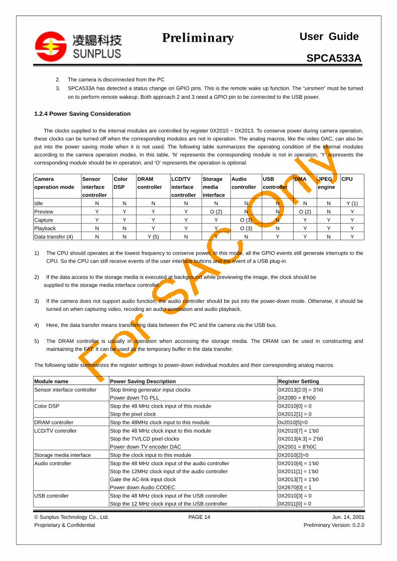
The clocks supplied to the internal modules are controlled by register 0X2010 ~ 0X2013. To conserve power during camera operation,
these clocks can be turned off when the corresponding modules are not in operation. The analog macros, like the video DAC, can also be
put into the power saving mode when it is not used. The following table summarizes the operating condition of the internal modules
according to the camera operation modes. In this table, ‘N’ represents the corresponding module is not in operation, ‘Y’ represents the
corresponding module should be in operation, and ‘O’ represents the operation is optional.
Camera
operation mode
Sensor
interface
controller
Color
DSP
DRAM
controller
LCD/TV
interface
controller
Storage
media
interface
Audio
controller
USB
controller
DMA JPEG
engine
CPU
Idle N N N N N N N N N Y (1)
Preview Y Y Y Y O (2) N N O (2) N Y
Capture Y Y Y Y Y O (3) N Y Y Y
Playback N N Y Y Y O (3) N Y Y Y
Data transfer (4) N N Y (5) N Y N Y Y N Y
1) The CPU should operates at the lowest frequency to conserve power. In this mode, all the GPIO events still generate interrupts to the
CPU. So the CPU can still receive events of the user interface buttons and the event of a USB plug-in.
2) If the data access to the storage media is executed at background while previewing the image, the clock should be
supplied to the storage media interface controller.
3) If the camera does not support audio function, the audio controller should be put into the power-down mode. Otherwise, it should be
turned on when capturing video, recoding an audio annotation and audio playback.
4) Here, the data transfer means transferring data between the PC and the camera via the USB bus.
5) The DRAM controller is usually in operation when accessing the storage media. The DRAM can be used in constructing and
maintaining the FAT. It can be used as the temporary buffer in the data transfer.
The following table summarizes the register settings to power-down individual modules and their corresponding analog macros.
Module name Power Saving Description Register Setting
Sensor interface controller Stop timing generator input clocks
Power down TG PLL
0X2013[2:0] = 3’h0
0X2080 = 8’h00
Color DSP Stop the 48 MHz clock input of this module
Stop the pixel clock
0X2010[0] = 0
0X2012[1] = 0
DRAM controller Stop the 48MHz clock input to this module 0x2010[5]=0
LCD/TV controller Stop the 48 MHz clock input to this module
Stop the TV/LCD pixel clocks
Power down TV encoder DAC
0X2010[7] = 1’b0
0X2013[4:3] = 2’b0
0X2001 = 8’h0C
Storage media interface Stop the clock input to this module 0X2010[2]=0
Audio controller Stop the 48 MHz clock input of the audio controller
Stop the 12MHz clock input of the audio controller
Gate the AC-link input clock
Power down Audio CODEC
0X2010[4] = 1’b0
0X2011[1] = 1’b0
0X2013[7] = 1’b0
0X2670[0] = 1
USB controller Stop the 48 MHz clock input of the USB controller
Stop the 12 MHz clock input of the USB controller
0X2010[3] = 0
0X2011[0] = 0

SPCA533A
© Sunplus Technology Co., Ltd.
Proprietary & Confidential
PAGE 15 Jun. 14, 2001
Preliminary Version: 0.2.0
Preliminary User Guide
Power down USB transceiver 0X2005[0] = 1
DMA Stop the clock input to this module 0x2010[1] = 0
JPEG Stop the 48 MHz clock input to this module 0X2010[6] = 0
CPU Set the CPU operating clock to the lowest frequency 0X2024[2]=3’h7
1.2.5 User Interface
The SPCA533A communicates with the UI module (Sunplus SPL10A) via a 3-pin serial interface. The SPL10A is the Sunplus UI
module, which integrates a status LCD and the key-scan function. The SPCA533A may send data to the UI module. For example the picture
count can be sent to the UI module and displayed on the status LCD. The SPCA533A can also read the key status from the UI module. The
interconnection between the SPCA533A and SPL10A is shown below.
STB
DAT
ACK
SPCA533 UI Processor
The SPL10A acts as a slave in the camera system. It dos not send data to the SPCA533A spontaneously. The SPCA533A reads the
key status on the UI module periodically and interrupts the micro-controller. This polling procedure is done by hardware and the polling
interval is programmable. In cases that user inputs be sent to the micro-controller in real time, the GPIO pins of the SPCA533A should be
connected to the user input instead. Because the user input via the UI module is read by the SPCA533A periodically and does not guarantee
to be delivered in real time. Also, if the user input is used to wake up the SPCA533A from the suspend state, it should also be connected to
the SPCA533A GPIO pins, too. Because the SPCA533A stops the polling procedure in the suspend state.
The following timing diagram shows the communication protocol between the SPCA533A and SPL10A.
D15D14D13D12D11D10D9 D8 D7 D6 D5 D4 D3 D2 D1 D0
STB
DAT
ACK
STB
DAT
ACK
Synchronization bit set low Synchronization bit set low
Acknowledge low for host Acknowledge high for host
Transform Data

SPCA533A
© Sunplus Technology Co., Ltd.
Proprietary & Confidential
PAGE 16 Jun. 14, 2001
Preliminary Version: 0.2.0
Preliminary User Guide
1 0 1 X A3 A2 A1 A0 D7 D6 D5 D4 D3 D2 D1 D0
STB
DAT
ACK
1 1 0 X X X X X D7 D6 D5 D4 D3 D2 D1 D0
STB
DAT
ACK
1 0 0 D4 D3 D2 D1 D0
STB
DAT
ACK
1 1 1 X X X X X
STB
DAT
ACK
Write Command
Read Command
Set Command
Sleep Command
Transmit data to the UI module : set the UITxReq high and then poll for the UITxRxCmplt bit. After the UITxRxCmplt bit is detected high,
write the data to the UITxData port and poll for the UITxRxCmplt again. After the UITxRxCmplt becomes high, the data has been
successfully transmitted to the UI module. The firmware must deassert the UITxReq at the end.
Put the UI module into sleep : The STB singal stays low after 8-bit data is transferred.
Wakeup the UI module : Set the UITxReq high and wait for the UITxRxCmplt bit becomes high. The UITxRxCmplt bit will become high after
the UI module is back to its normal operation state.
Read data from the UI module: The hardware of the SPCA533A polls the UI module automatically. If a non-zero data is read, an interrupt
will be generated to inform the CPU. The CPU then read the data and clear the interrupt. To change the polling interval, disable the UIIntEn
first and write the desired value to the UIPollingIntval in millisecond. The default value of the UIPollingIntval is 1 ms and the range is from 1
to 255 ms. Enable the UIIntEn before returning to the normal polling operation.

SPCA533A
© Sunplus Technology Co., Ltd.
Proprietary & Confidential
PAGE 17 Jun. 14, 2001
Preliminary Version: 0.2.0
Preliminary User Guide
UI control flow
Wake SPL10A Up
Done
Set UITxReq
UITxRxCmplt
no
yes
Clear UITxReq
Disable UIIntEn
Set UIPollingIntvl
Enable UIIntEn
Done
Change UIPollingIntvlReceive data from UI processor
UIint
Read UIRxData
Clear UIint
Done
(Read command)
Write UITxData
Done
Transmit data to UI processor
Set UITxReq
UITxRxCmplt
no
yes
UITxRxCmplt
no
yes
Clear UITxReq
(Write, Set and Sleep command)
1.2.6 Global Timer Control
The SPCA533A has built-in a global timer, which counts based on 1 ms interval. This timer is a general-purpose timer. The application
may use it to do time measurement or uses it a watch-dog timer. The timer is operated either in the upcount mode or the downcount mode.
In the upcount mode, the timer simply reports how many ms have passed after it is triggered. In the downcount mode, an initial timer value
must be programmed before the timer is triggered, then the timer will decrement for every 1 ms. The downcount mode can be use as an
watch-dog timer, which reset the CPU while the timer value downcounts to 0.
Set initial timer value(optional)
Upcount mode Downcount mode
Set upcount=1
set startTimer=1 (trigger)
Polling timervalues
Set initial timer value(optional)
Set upcount=0
set startTimer=1 (trigger)
waiting forinterrupt

SPCA533A
© Sunplus Technology Co., Ltd.
Proprietary & Confidential
PAGE 18 Jun. 14, 2001
Preliminary Version: 0.2.0
Preliminary User Guide
1.2.7 RTC
The SPCA533’s built-in RTC (real time clock) consists of an 48-bit counter. The frequency of the input clock to the RTC is 32.768 kHz. The
value of the counter is translated to year, date, and time by the firmware. Sunplus provides the translation firmware to the customers. The
power supply to the RTC module is separated from the power supply to the other part of the SPCA533. While the SPCA533A is powered
down, the application must keep supplying power to the RTC to maintain RTC operation. Separating the powers guarantees minimum
current leakage.
The internal registers of the RTC module can be accessed according to the flow below.
Set RTC Address(0X206B)
Set RTC Write Data(0X206C)
Trigger RTC Write(0X2069 Bit 0)
Polling RTC Ready(0X206A bit 0)
Yes
No
Done
Write RTC Internal Register
Set RTC Address(0X206B)
Read RTC Internal Register
Trigger RTC Read(0X2069 Bit 1)
Polling RTC Ready(0X206A bit 0)
YesNo
Done
Read RTC Data(0X206D)
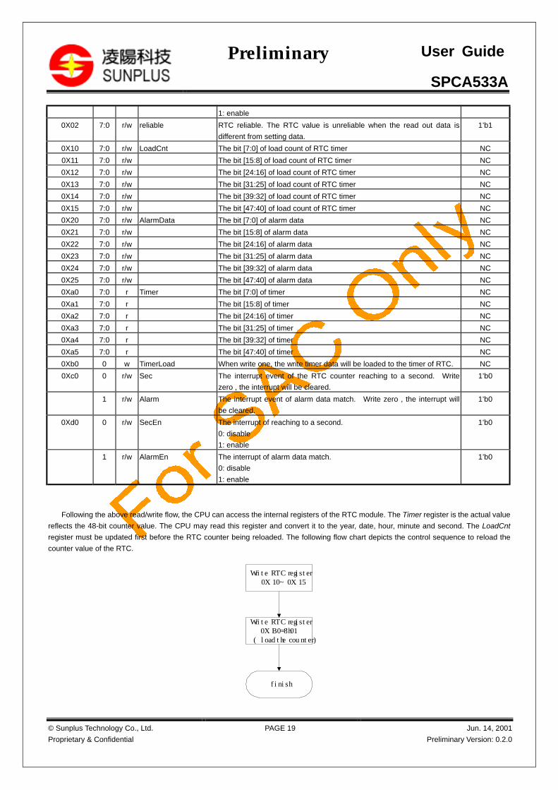
RTC module registers
Address Bit Att Name Description Default
value
0X00 0 r/w RTCEn RTC
0: disable
1: enable
1’b1
1 r/w RTCRst RTC
0: normal
1: reset
1’b0
2 r/w TimerDir Timer direction (the count of the timer is to down count or to up count
when the RTC clock is from high to low)
0: down count
1: up count
1’b1
0X01 0 r/w RRP RTC RRP (register reduce power) signal.
0: disable
1’b0
SPCA533A
© Sunplus Technology Co., Ltd.
Proprietary & Confidential
PAGE 19 Jun. 14, 2001
Preliminary Version: 0.2.0
Preliminary User Guide
1: enable
0X02 7:0 r/w reliable RTC reliable. The RTC value is unreliable when the read out data is
different from setting data.
1’b1
0X10 7:0 r/w LoadCnt The bit [7:0] of load count of RTC timer NC
0X11 7:0 r/w The bit [15:8] of load count of RTC timer NC
0X12 7:0 r/w The bit [24:16] of load count of RTC timer NC
0X13 7:0 r/w The bit [31:25] of load count of RTC timer NC
0X14 7:0 r/w The bit [39:32] of load count of RTC timer NC
0X15 7:0 r/w The bit [47:40] of load count of RTC timer NC
0X20 7:0 r/w AlarmData The bit [7:0] of alarm data NC
0X21 7:0 r/w The bit [15:8] of alarm data NC
0X22 7:0 r/w The bit [24:16] of alarm data NC
0X23 7:0 r/w The bit [31:25] of alarm data NC
0X24 7:0 r/w The bit [39:32] of alarm data NC
0X25 7:0 r/w The bit [47:40] of alarm data NC
0Xa0 7:0 r Timer The bit [7:0] of timer NC
0Xa1 7:0 r The bit [15:8] of timer NC
0Xa2 7:0 r The bit [24:16] of timer NC
0Xa3 7:0 r The bit [31:25] of timer NC
0Xa4 7:0 r The bit [39:32] of timer NC
0Xa5 7:0 r The bit [47:40] of timer NC
0Xb0 0 w TimerLoad When write one, the write timer data will be loaded to the timer of RTC. NC
0Xc0 0 r/w Sec The interrupt event of the RTC counter reaching to a second. Write
zero , the interrupt will be cleared.
1’b0
1 r/w Alarm The interrupt event of alarm data match. Write zero , the interrupt will
be cleared.
1’b0
0Xd0 0 r/w SecEn The interrupt of reaching to a second.
0: disable
1: enable
1’b0
1 r/w AlarmEn The interrupt of alarm data match.
0: disable
1: enable
1’b0
Following the above read/write flow, the CPU can access the internal registers of the RTC module. The Timer register is the actual value
reflects the 48-bit counter value. The CPU may read this register and convert it to the year, date, hour, minute and second. The LoadCnt
register must be updated first before the RTC counter being reloaded. The following flow chart depicts the control sequence to reload the
counter value of the RTC.
Write RTC register 0X10~0X15
Write RTC register 0XB0=8'h01(load the counter)
finish
SPCA533A
© Sunplus Technology Co., Ltd.
Proprietary & Confidential
PAGE 20 Jun. 14, 2001
Preliminary Version: 0.2.0
Preliminary User Guide
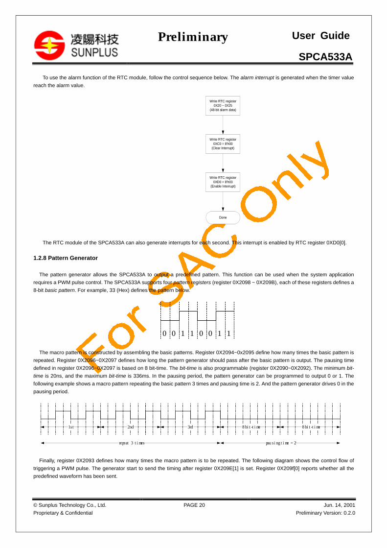
To use the alarm function of the RTC module, follow the control sequence below. The alarm interrupt is generated when the timer value
reach the alarm value.
Write RTC register0X20 ~ 0X25
(48-bit alarm data)
Write RTC register0XC0 = 8'h00
(Clear Interrupt)
Done
Write RTC register0XD0 = 8'h03
(Enable Interrupt)
The RTC module of the SPCA533A can also generate interrupts for each second. This interrupt is enabled by RTC register 0XD0[0].
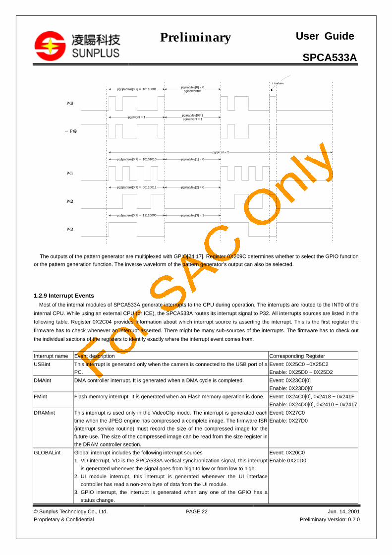
1.2.8 Pattern Generator
The pattern generator allows the SPCA533A to output a predefined pattern. This function can be used when the system application
requires a PWM pulse control. The SPCA533A supports four pattern registers (register 0X2098 ~ 0X209B), each of these registers defines a
8-bit basic pattern. For example, 33 (Hex) defines the pattern below.
0 0 1 1 0 0 1 1
The macro pattern is constructed by assembling the basic patterns. Register 0X2094~0x2095 define how many times the basic pattern is
repeated. Register 0X2096~0X2097 defines how long the pattern generator should pass after the basic pattern is output. The pausing time
defined in register 0X2096~0X2097 is based on 8 bit-time. The bit-time is also programmable (register 0X2090~0X2092). The minimum bit-
time is 20ns, and the maximum bit-time is 336ms. In the pausing period, the pattern generator can be programmed to output 0 or 1. The
following example shows a macro pattern repeating the basic pattern 3 times and pausing time is 2. And the pattern generator drives 0 in the
pausing period.
1st 2nd 3rd 8 bit-time 8 bit-time
repeat 3 times pausing time = 2
Finally, register 0X2093 defines how many times the macro pattern is to be repeated. The following diagram shows the control flow of
triggering a PWM pulse. The generator start to send the timing after register 0X209E[1] is set. Register 0X209f[0] reports whether all the
predefined waveform has been sent.

SPCA533A
© Sunplus Technology Co., Ltd.
Proprietary & Confidential
PAGE 21 Jun. 14, 2001
Preliminary Version: 0.2.0
Preliminary User Guide
Set Time Base(0X2090 ~ 0X2092)
Set Active Count(0X2094 ~ 0X2095)
Set Inactive Count(0X2096 ~ 0X2097)
Select Ouput GPIO(0X209C)
Set Trigger Source(0X209E)
Polling PGReady
(0X209F bit 0)
YesNo
Done
Set Repeat Count(0X2093)
Set Pattern(0X2098 ~ 0X209b)
Set Inactive level(0X209d)
The above diagram shows triggering the pattern generator in manual mode. The pattern generator can also be triggered by the mechnical
shutter control signal. Register 0X209E[0] controls whether to select the trigger source as the mechanical shutter control signal (mshutter).
The timing of mshutter is defined in the CCD sensor section. If the mshutter is selected as the triggering source, the predefined pattern will
be sent whenever the state of the mshutter changes (from high to low or from low to high).
The following diagram is a example of programming the pattern generator:
SPCA533A
© Sunplus Technology Co., Ltd.
Proprietary & Confidential
PAGE 22 Jun. 14, 2001
Preliminary Version: 0.2.0
Preliminary User Guide
PG0
~PG0
PG1
PG2
pgatvcnt = 1pginatvlev[0]=1pginatvcnt = 1
pgrptcnt = 2
timebase
pginatvlev[0] = 0pginatvcnt=1
pg0pattern[0:7] = 10110001
pg1pattern[0:7] = 10101010
pg2pattern[0:7] = 00110011
PG2
pg3pattern[0:7] = 11110000
pginatvlev[1] = 0
pginatvlev[2] = 0
pginatvlev[3] = 1
The outputs of the pattern generator are multiplexed with GPIO[24:17]. Register 0X209C determines whether to select the GPIO function
or the pattern generation function. The inverse waveform of the pattern generator’s output can also be selected.
1.2.9 Interrupt Events
Most of the internal modules of SPCA533A generate interrupts to the CPU during operation. The interrupts are routed to the INT0 of the
internal CPU. While using an external CPU (or ICE), the SPCA533A routes its interrupt signal to P32. All interrupts sources are listed in the
following table. Register 0X2C04 provides information about which interrupt source is asserting the interrupt. This is the first register the
firmware has to check whenever an interrupt asserted. There might be many sub-sources of the interrupts. The firmware has to check out
the individual sections of the registers to identify exactly where the interrupt event comes from.
Interrupt name Event description Corresponding Register
USBint This interrupt is generated only when the camera is connected to the USB port of a
PC.
Event: 0X25C0 ~0X25C2
Enable: 0X25D0 ~ 0X25D2
DMAint DMA controller interrupt. It is generated when a DMA cycle is completed. Event: 0X23C0[0]
Enable: 0X23D0[0]
FMint Flash memory interrupt. It is generated when an Flash memory operation is done. Event: 0X24C0[0], 0x2418 ~ 0x241F
Enable: 0X24D0[0], 0x2410 ~ 0x2417
DRAMint This interrupt is used only in the VideoClip mode. The interrupt is generated each
time when the JPEG engine has compressed a complete image. The firmware ISR
(interrupt service routine) must record the size of the compressed image for the
future use. The size of the compressed image can be read from the size register in
the DRAM controller section.
Event: 0X27C0
Enable: 0X27D0
GLOBALint Global interrupt includes the following interrupt sources
1. VD interrupt, VD is the SPCA533A vertical synchronization signal, this interrupt
is generated whenever the signal goes from high to low or from low to high.
2. UI module interrupt, this interrupt is generated whenever the UI interface
controller has read a non-zero byte of data from the UI module.
3. GPIO interrupt, the interrupt is generated when any one of the GPIO has a
status change.
Event: 0X20C0
Enable 0X20D0

SPCA533A
© Sunplus Technology Co., Ltd.
Proprietary & Confidential
PAGE 23 Jun. 14, 2001
Preliminary Version: 0.2.0
Preliminary User Guide
4. Global timer interrupt. This interrupt is generated when the global timer down
counts to zero.
5. RTC event interrupt: This interrupt is generated when the bit of “second” of the
RTC counter is changed or the counter reaches to the setting of alarm.
Digtvint Digital TV interrupt includes the following interrupt sources
1. TVENC VD interrupt, TVENC VD is the SPCA533A TV encoder vertical
synchronization signal, this interrupt is generated whenever the signal goes
from high to low or from low to high.
2. GPIO interrupt, the interrupt is generated when any one of the digital TV port
has a status change.
Event: 0X2DC0~0X2DC6
Enable 0X2DD0~0X2DD6
Audioint Audio interrupt sources are the following:
1. Audio buffer over high threshold or audio buffer under low threshold
2. MPFCEB from the MP3 processor goes from low to high
Event: 0X26C0 ~ 0X26C1
Enable: 0X26D0 ~ 0X26D1
1.3 CDSP
The CDSP (Color DSP) of the SPCA533A is a hard-wired image processing engine. In the preview mode, the image with width over 480
pixels must be scaled down in the RGB domain as the first step of the image processing. This is for speeding up the image processing. In
the full frame capture mode, the raw data can be stored in the SDRAM first and waited for further process. There is a horizontal scale-down
engine in SPCA533A that can be programmed to scale the image to the required size. The image processing is a pipelined architecture,
which will be described in the hardwired processor sub-section.
1.3.1 Image size limitation
The first step to snap an image is to capture the raw data and store it into the SDRAM. The following diagram shows the control flow.
This control flow applies to both progressive sensors and the interlace sensors. If the interlace sensors is connected to the SPCA533, the
line sequence is adjusted automatically to make the final raw data fit the Bayer pattern format. The result is stored in the raw data buffer. The
starting address of the raw data buffer is defined in the register 0X2768~0X276A. The following diagram shows an example to capture an
1296x972 raw data.
Polling Capture Done
(0X27B0 bit 1)
NoYes
Done
Start CDSP(0X2712 bit 0 = 1)(0X2000 = 8'h00)(0X2000 = 8'h02)(0X27A1 bit4 = 1)
Set Raw Buffer Starting Address(0X2768 ~ 0X276A)
Set Raw Buffer Horizontal Width = 12960X27F4 = 8'h100X27F5 = 8'h05
Set Raw Buffer Vertical Size = 9720X276D = 8'hCC 0X276E = 8'h03
Set Raw Buffer Horizontal Offset = 00X27FA = 8'h000X27FB = 8'h00
Set Raw Buffer Horizontal Size = 12960X276B = 8'h10 0X276C = 8'h05
Capture 1296x972 Image of Raw data
The next step of snapping an image is partitioning the image into stripes with width 480 pixels, putting them in to the CDSP and store the
output data to the SDRAM again. After the processing, the image is converted into the YUV domain and will be stored into the A-frame buffer.
SPCA533A
© Sunplus Technology Co., Ltd.
Proprietary & Confidential
PAGE 24 Jun. 14, 2001
Preliminary Version: 0.2.0
Preliminary User Guide
The starting address of the A-frame buffer is defined in register 0X2753~0X2755. In the partition, each stripe must has 16 pixels’ overlap
area with the adjacent stripe to cover the boundaries condition. The following diagram shows an example of partitioning an 1296x972 raw
data. The target is to generate a 1280x960 YUV data.
data in the raw data buffer
480 pixels(1st stripe)
480pixels(2nd stripe)
368 pixels(3rd stripe)
1296 pixels
972pixels
16 pixels
1st stripe
2nd stripe
3rd stripe
data in the A-frame buffer (YUV422)
8 pixels
8 pixels
8 pixels
8 pixels
8 pixels
8 pixels
1280 pixels
960 pixels
464928
The width of the raw data is 1296, which needs to be partitioned into 3 stripes. The control flow is in the following in the following
diagram. Note that the with of the last stripe is only 268 pixels.

SPCA533A
© Sunplus Technology Co., Ltd.
Proprietary & Confidential
PAGE 25 Jun. 14, 2001
Preliminary Version: 0.2.0
Preliminary User Guide
Set Raw Buffer Starting Address(0X2768 ~ 0X276A)
Set Raw Buffer Horizontal Width = 12960X27F4 = 8'h100X27F5 = 8'h05
Set Raw Buffer Vertical Size = 9720X276D = 8'hCC 0X276E = 8'h03
Programming CDSP Register
Cut and Paste from 1296x972 to 1280x960 Image without Horizontal Mirror
Polling Capture Done
(0X27B0 bit 1)
No
Set A Frame Buffer Starting Address(0X2753 ~ 0X2755)
Set A Frame Buffer Horizontal Width = 12800X27F0 = 8'h000X27F1 = 8'h05
1st stripe
Start CDSP(0X2712 bit 0 = 1)(0X2000 = 8'h00)(0X2000 = 8'h02)(0X27A1 bit4 = 1)
Set A Frame Buffer Vertical Size = 9600X2762 = 8'hC0 0X2763 = 8'h03
Set Raw Buffer Horizontal Offset = 00X27FA = 8'h000X27FB = 8'h00
Set Raw Buffer Horizontal Size = 4800X276B = 8'hE0 0X276C = 8'h01
Set A Frame Buffer Horizontal Offset = 00X27F6 = 8'h000X27F7 = 8'h00
Set A Frame Buffer Horizontal Size = 4640X2760 = 8'hD00X2761 = 8'h01
Yes
2nd stripe
Polling Capture Done
(0X27B0 bit 1)
No
Start CDSP(0X2712 bit 0 = 1)(0X2000 = 8'h00)(0X2000 = 8'h02)(0X27A1 bit4 = 1)
Set Raw Buffer Horizontal Offset = 4640X27FA = 8'hD00X27FB = 8'h01
Set Raw Buffer Horizontal Size = 4800X276B = 8'hE0 0X276C = 8'h01
Set A Frame Buffer Horizontal Offset = 4640X27F6 = 8'hD00X27F7 = 8'h01
Set A Frame Buffer Horizontal Size = 4640X2760 = 8'hD00X2761 = 8'h01
Yes
3rd stripe
Polling Capture Done
(0X27B0 bit 1)
No
Start CDSP(0X2712 bit 0 = 1)(0X2000 = 8'h00)(0X2000 = 8'h02)(0X27A1 bit4 = 1)
Set Raw Buffer Horizontal Offset = 9280X27FA = 8'hA00X27FB = 8'h03
Set Raw Buffer Horizontal Size = 3680X276B = 8'h70 0X276C = 8'h01
Set A Frame Buffer Horizontal Offset = 9280X27F6 = 8'hA00X27F7 = 8'h03
Set A Frame Buffer Horizontal Size = 3520X2760 = 8'h600X2761 = 8'h01
Yes
Done
The exposure and white-balance control registers are usually programmed when the camera is in preview mode. The snapped image
will use the AE/AWB window values measured in the preview mode. However, when the flash light is applied to the image, the white-balance
might need to be adjusted further due to the color temperature change. The SPCA533A allows the user to repeatedly programming the
exposure and white-balance control registers, performing the window measurement and read back the window values. This task is executed
similar to a standard image processing stated above, but the YUV data is not written back to the SDRAM (controlled by register 0x27F0[0]).
Also, the raw data must be sub-sampled if the width of the raw image is over 480 pixels (controlled by register 0X27FC). The following
diagram shows the control sequence.

SPCA533A
© Sunplus Technology Co., Ltd.
Proprietary & Confidential
PAGE 26 Jun. 14, 2001
Preliminary Version: 0.2.0
Preliminary User Guide
Set Raw Buffer Starting Address(0X2768 ~ 0X276A)
Set Raw Buffer Horizontal Size(0X276B ~ 0X276C)
Set Raw Buffer Vertical Size
(0X276D ~ 0X276E)
Programming CDSP and CDSP Window Register
Pre-CDSP (Get AE/AWB Window Values)
Get AE/AWB Window Value
Polling Pre-CDSP Done
(0X27B0 bit 3)
YesNo
Done
Set Raw Buffer Horizontal Width(0X27F4 ~ 0X27F5)
Set Raw Buffer Horizontal Offset(0X27FA ~ 0X27FB)
Skip CDSP YUV data(0X27F0 bit 0 = 1)
Start CDSP(0X2712 bit 0 = 1)(0X2000 = 8'h02)(0X27A1 bit4 = 1)
Set Horizontal and Vertical Window Sub-Sample Scale(0X27FC)
1.3.2 Horizontal Mirror on Raw Data
Due to the color interpolation and edge enhancement, the SPCA533A need some extra pixels on the four side of the raw data. In the
horizontal direction, the SPCA533A requires 16 extra pixels. And in the vertical direction, it requires 12 extra lines. For example, to get an
image of size 1280x960, the SPCA533A requires the raw image input of size 1296x972. If the sensor does not provides enough valid pixels,
the raw data mirror function should be turned on.
In the vertical direction, the SPCA533A supports two methods to extend the extra lines. The first one is to mirror the lines by the
copy&paste engine in the DRAM controller. This method physically copy the data and duplicate them in the SDRAM before the color
processing. It can be used only in the still image capture mode. In the video capture mode, there is not enough time to do the copy&paste
task, and the JPEG will need to insert lines when it read out the image from the SDRAM. The second approach is described in more details
in JPEG interface sub-section.
In the horizontal direction, the CDSP can mirror the image in real time. When this function is turned on (register0x2105[0]), the CDSP
automatically mirror 8 pixels at the front side of the raw image and 16 pixels at the rear side of the raw image.
G0
R0
G1
R1
G2
R2
G3
R3
G3
R3
G2
R2
G1
R1
G0
R0
The extra 8 pixels of horizontal mirror in the front side
G4
R4
G5
R5
G6
R6
G7
R7
G7
R7
G6
R6
G5
R5
G4
R4
The extra 16 pixels of horizontal mirror in the rear side
B0
G0
B1
G1
B2
G2
B3
G3
B3
G3
B2
G2
B1
G1
B0
G0
B4
G4
B5
G5
B6
G6
B7
G7
B7
G7
B6
G6
B5
G5
B4
G4
If the pixel mirroring function is turned on, the partition of the raw data (into stripes) should be modified. The following diagram shows
how to partition an image with raw size 1280x972, assuming the extra line extension is already done by the copy&paste engine of the DRAM
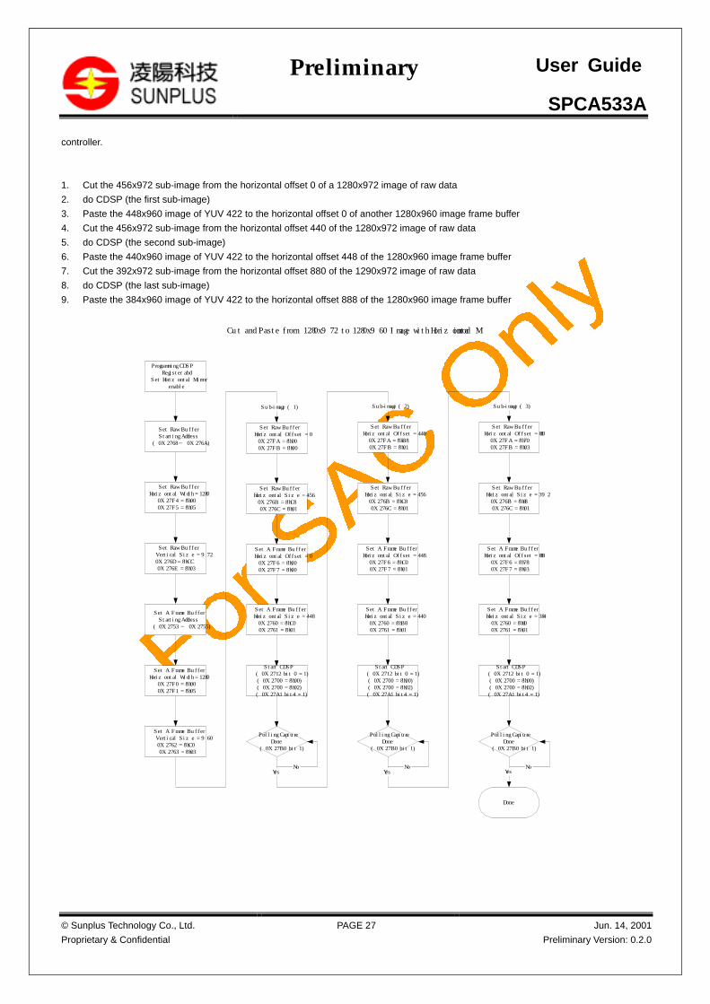
SPCA533A
© Sunplus Technology Co., Ltd.
Proprietary & Confidential
PAGE 27 Jun. 14, 2001
Preliminary Version: 0.2.0
Preliminary User Guide
controller.
1. Cut the 456x972 sub-image from the horizontal offset 0 of a 1280x972 image of raw data
2. do CDSP (the first sub-image)
3. Paste the 448x960 image of YUV 422 to the horizontal offset 0 of another 1280x960 image frame buffer
4. Cut the 456x972 sub-image from the horizontal offset 440 of the 1280x972 image of raw data
5. do CDSP (the second sub-image)
6. Paste the 440x960 image of YUV 422 to the horizontal offset 448 of the 1280x960 image frame buffer
7. Cut the 392x972 sub-image from the horizontal offset 880 of the 1290x972 image of raw data
8. do CDSP (the last sub-image)
9. Paste the 384x960 image of YUV 422 to the horizontal offset 888 of the 1280x960 image frame buffer
Set Raw Buffer Starting Address(0X2768 ~ 0X276A)
Set Raw Buffer Horizontal Width = 12800X27F4 = 8'h000X27F5 = 8'h05
Set Raw Buffer Vertical Size = 9720X276D = 8'hCC 0X276E = 8'h03
Programming CDSP Register abd
Set Horizontal Mirror enable
Cut and Paste from 1280x972 to 1280x960 Image with Horizontal Mirror
Polling Capture Done
(0X27B0 bit 1)
No
Set A Frame Buffer Starting Address(0X2753 ~ 0X2755)
Set A Frame Buffer Horizontal Width = 12800X27F0 = 8'h000X27F1 = 8'h05
Sub-image (1)
Start CDSP(0X2712 bit 0 = 1)(0X2700 = 8'h00)(0X2700 = 8'h02)(0X27A1 bit4 = 1)
Set A Frame Buffer Vertical Size = 9600X2762 = 8'hC0 0X2763 = 8'h03
Set Raw Buffer Horizontal Offset = 00X27FA = 8'h000X27FB = 8'h00
Set Raw Buffer Horizontal Size = 4560X276B = 8'hC8 0X276C = 8'h01
Set A Frame Buffer Horizontal Offset = 00X27F6 = 8'h000X27F7 = 8'h00
Set A Frame Buffer Horizontal Size = 4480X2760 = 8'hC00X2761 = 8'h01
Yes
Sub-image (2)
Polling Capture Done
(0X27B0 bit 1)
No
Start CDSP(0X2712 bit 0 = 1)(0X2700 = 8'h00)(0X2700 = 8'h02)(0X27A1 bit4 = 1)
Set Raw Buffer Horizontal Offset = 4400X27FA = 8'hB80X27FB = 8'h01
Set Raw Buffer Horizontal Size = 4560X276B = 8'hC8 0X276C = 8'h01
Set A Frame Buffer Horizontal Offset = 4480X27F6 = 8'hC00X27F7 = 8'h01
Set A Frame Buffer Horizontal Size = 4400X2760 = 8'hB80X2761 = 8'h01
Yes
Sub-image (3)
Polling Capture Done
(0X27B0 bit 1)
No
Start CDSP(0X2712 bit 0 = 1)(0X2700 = 8'h00)(0X2700 = 8'h02)(0X27A1 bit4 = 1)
Set Raw Buffer Horizontal Offset = 8800X27FA = 8'h700X27FB = 8'h03
Set Raw Buffer Horizontal Size = 3920X276B = 8'h88 0X276C = 8'h01
Set A Frame Buffer Horizontal Offset = 8880X27F6 = 8'h780X27F7 = 8'h03
Set A Frame Buffer Horizontal Size = 3840X2760 = 8'h800X2761 = 8'h01
Yes
Done

SPCA533A
© Sunplus Technology Co., Ltd.
Proprietary & Confidential
PAGE 28 Jun. 14, 2001
Preliminary Version: 0.2.0
Preliminary User Guide
392
With horizontal mirrow
1280
1280x972 image
16
400
880
1280
0
448 8
456
0
1280
0
8 16
440 8
456
440
8 168
8 8
the horizontal mirror 8 pixels in the front side
the overlap 16 pixels in the middle part
the overlap 16 pixels in the middle part
the horizontal mirror 16 pixels in the rear side
Original Image
Overlap Image
Horizontal Mirror Image
1.3.3 Horizontal Scale Down on Raw Data
SPCA533A builds in a real-time horizontal scale down engine in the CDSP to scale down the width of the raw image. This function is
used in the preview mode or PC-camera mode in which real time image rendering is required. To enable the scale down function, set
register 0X271A[0] to 1. The target-to-source image size ratio, is programmable in register 0X271B and 0X21C, which is a 16 bit fractional
number.
Example: , horizontally scale down a 1280x240 image to a 320x240 image.
scale down ratio = 320/1280
scale down ratio factor = the upper bound integer of (320/1280)*65536 = 16384 (0X4000)
Set register 0X211B = 8’h00
register 0X211C = 8’h40
1.3.4 Hardwired Color Processor
The hardwired color DSP performs following tasks: optical black compensation, bad pixel compensation, white balance adjustment, color
interpolation, color correction, gamma correction, RGB-to-YUV conversion, 2D-edge enhancement, bright adjustment, contrast adjustment,
saturation adjustment, hue adjustment, white balance window statistics, exposure window statistics and focus window statistics.
Data Format:
The Color DSP receives 10-bit RGB Bayer pattern data, and output 8-bit YUV 422 data.

SPCA533A
© Sunplus Technology Co., Ltd.
Proprietary & Confidential
PAGE 29 Jun. 14, 2001
Preliminary Version: 0.2.0
Preliminary User Guide
Register Update:
All of the CDSP registers take effect right after they are programmed except registers for white balance (0x2120 ~ 2128) and auto
focusing (0x2210 ~ 2215) windows, which are effective until the next the start of the next image frame.
Real time Bad Pixel Correction:
At the power-on stage of the SPCA533A, the coordinates of the bad pixels must be loaded into the internal registers of the CDSP. This
information is used for the real time bad-pixel correction. The SPCA533A can correct up to 256 bad pixels in the real time bad pixel
correction. The value of the bad pixel is replaced by the value nearest pixel of the same type. The following diagrams shows the control flow
to load the bad pixel coordinates. The programming sequence of bad pixel coordinates must be from left to right and from up to down that is
the same as the processing sequence of CDSP. If the bad pixel number is small than 256, the content of the next index after the last bad-
pixel on the bad-pixel SRAM must be programmed to the value of 0XFFFFFF that is as a terminator of bad-pixel SRAM.
no
Done
Write bad pixel SRAM index
0X2115 = n
Write the horizontal coordinate of bad pixel
0X21110X2112
Write the vertical coordinate of bad pixel
0X21130X2114
Bad Pixel SRAM Programming
Bad Pixel SRAM Programming Enable0X2110 = 8'h02
n = 0
Program complete
next bad pixeln = n+1
no
Write bad pixel SRAM index
0X2115 = n
Write the horizontal coordinate of bad pixel0X2111 = 8'hff0X2112 = 8'h0f
Write the vertical coordinate of bad pixel0X2113 = 8'hff0X2114 = 8'h0f
n == 256
ad Pixel SRAM Programming Disable0X2110 = 8'h00
yes yes
For the still image capture, the bad-pixel correction engine in the DRAM controller can fix the bad-pixel with better quality. The number of
the bad pixels that can be fixed in the still image capture is unlimited.

SPCA533A
© Sunplus Technology Co., Ltd.
Proprietary & Confidential
PAGE 30 Jun. 14, 2001
Preliminary Version: 0.2.0
Preliminary User Guide
Optical Black:
The optical black compensation is applied to the raw data image as the first step of the color processing. The SPCA533A supports two
methods of optical black compensation. The first method requires the user to define a value in the manual optical black level register. The
CDSP subtract this value from all the input pixel values. The other method requires the user to define a rectangle region named optical black
window. The optical black window should locate in the sensor area where pixel cells are shield from the light source. It could be at the top
side, left side, right side or bottom side of the pixel array of the sensor. The CDSP automatically calculate the mean value of the pixel data in
the optical black window and subtract the mean value from all the incoming pixel value. The size and shape of the optical black window are
also programmable. The type of OB window is defined in register 0X210A[6:4], the horizontal offset of OB window is defined in register
0X210C and 0X210B[3:0] and the vertical offset of OB window is defined in register 0X210D and 0X210B[7:4].
obtype=01x256
obtype=12x256
obtype=24x256
obtype=38x256
(obhoff,obvoff)
obtype=4 : 256x1obtype=5 : 256x2obtype=6 : 256x4obtype=7 : 256x8
(obhoff,obvoff)
The manual and automatic methods of the optical black compensation are turned on by individual control bits (register 0X201A[1:0]).
They can be turned simultaneously.
White Balance Adjustment:
Each component of the image raw data (R, Gr, B, Gb) may be respectively adjusted by programming its corresponding offset and gain.
The adjustment is done according to the following equation.
Output value = (Input value + offset) * gain
The offsets and gains are derived from the AWB (auto white balance) algorithm. The customers may customize their own AWB algorithm.
The offsets are defined in register 0X2120 ~ 0X2123 and the gains are defined in register 0X2124 ~ 0X2128.
ROM Gamma Correction:
After the white balance adjustment, the CDPS applies a gamma correction to the data. This gamma function is applied to all four
components (R, B, Gr and Gb) of the image data with the same fixed curve. A gamma ROM is embedded for this function. The ROM gamma
correction function can is turned on by setting register 0X2130[0] to 1.
Color Interpolation:
The missing color components in the Bayer pattern are derived in this stage with a SUNPLUS proprietary algorithm.
Color Correction:
The equation of the color correction is shown below. The parameters of the 3x3 martix are programmable.
Rout = A11 * Rin + A12 * Gin + A13 * Bin
Gout = A21 * Rin + A22 * Gin + A23 * Bin
Bout = A31 * Rin + A32 * Gin + A33 * Bin
These coefficients are defined in register 0X2140 ~ 0X2149.

SPCA533A
© Sunplus Technology Co., Ltd.
Proprietary & Confidential
PAGE 31 Jun. 14, 2001
Preliminary Version: 0.2.0
Preliminary User Guide
LUT Gamma Correction:
The users can optionally choose to do gamma correction after the color correction. The R, G, B components share the same gamma
curve. The gamma curve is constructed by a look-up table. The look-up table defines 17 points which represent 16 line segments. The y
coordinates of the 17 points are programmable with range from 0 to 255. the x coordinates of the 17 points are equal distance (16) to place
between 0 and 256 (the first point is 0 and the last point is to 256, the unit is 4 gray levels).
A programmable low-pass filer is applied to the gamma cure to smooth it. The low-pass filter is enabled by setting register 0X2130[1:0] =
2’b10. The low-pass filer is controlled by a smoothing factor d, which is programmed through register 0X2151.
R-B Clamping:
There is a programming clamping value (register 0X2131) to clamp R and B values. The clamping value is shared by R and B and there is
a bit (register 0X2130[1]) to enable the R and B clamping function.
RGB-to-YUV Transform:
RGB-to-YUV transform equation is shown below:
Y = G + 19*[(R-G)+24*(B-G)/64]/64
U = 32*[(B-G)-22*(R-G)/64]/64
V = 32*[(R-G)-10*(B-G)/64]/64
2D-Edge Enhancement:
This chip uses a SUNPLUS-proprietary algorithm for 2D-edge enhancement.
Low-pass filtering:
For Y component, a horizontal low-pass filtering can be applied to two adjacent pixels, three adjacent pixels or four adjacent pixels that
are programmed by register 0X21a5[1:0]. For U/V components, a low-pass filter can be applied to two horizontally adjacent pixels that is
enabled by register 0X21AB[0]. It can also be applied to two vertically adjacent pixels that is enabled by register 0X21AB[1].
Bright and Contrast Adjustment:
The function is enabled by register 0X21A6[0]. Y bright/contrast equation: (Y ranges from –512~511) The Contrast and Bright are
programmable in register 0X21A6 ~ 0X21A8.
Yout = Contrast * (Yin + Bright)
Saturation and Hue Adjustment:
The function is enabled by register 0X21AC[0]. UV saturation/hue equation: (U, V ranges from –512~511) The Sat and Hue are
programmable in 0X21AC ~ 0X21AE.
Uout = Sat * [ Uin * Cos(Hue) – Vin * Sin(Hue) ]
Vout = Sat * [ Uin * Sin(Hue) + Vin * Cos(Hue) ]
R, B Clamping for AWB Window Measurement:
There is a programming clamping value (register 0X2207) to clamp R and B value according to the following equations. The clamping
value is shared by R and B and there is a bit (register 0X2206[2]) to enable the R and B clamping function for AWB window measurement.
The clamping method is the as in the R-B clamping paragraph.
R-Y, B-Y Clamping to zero for AWB Window Measurement:
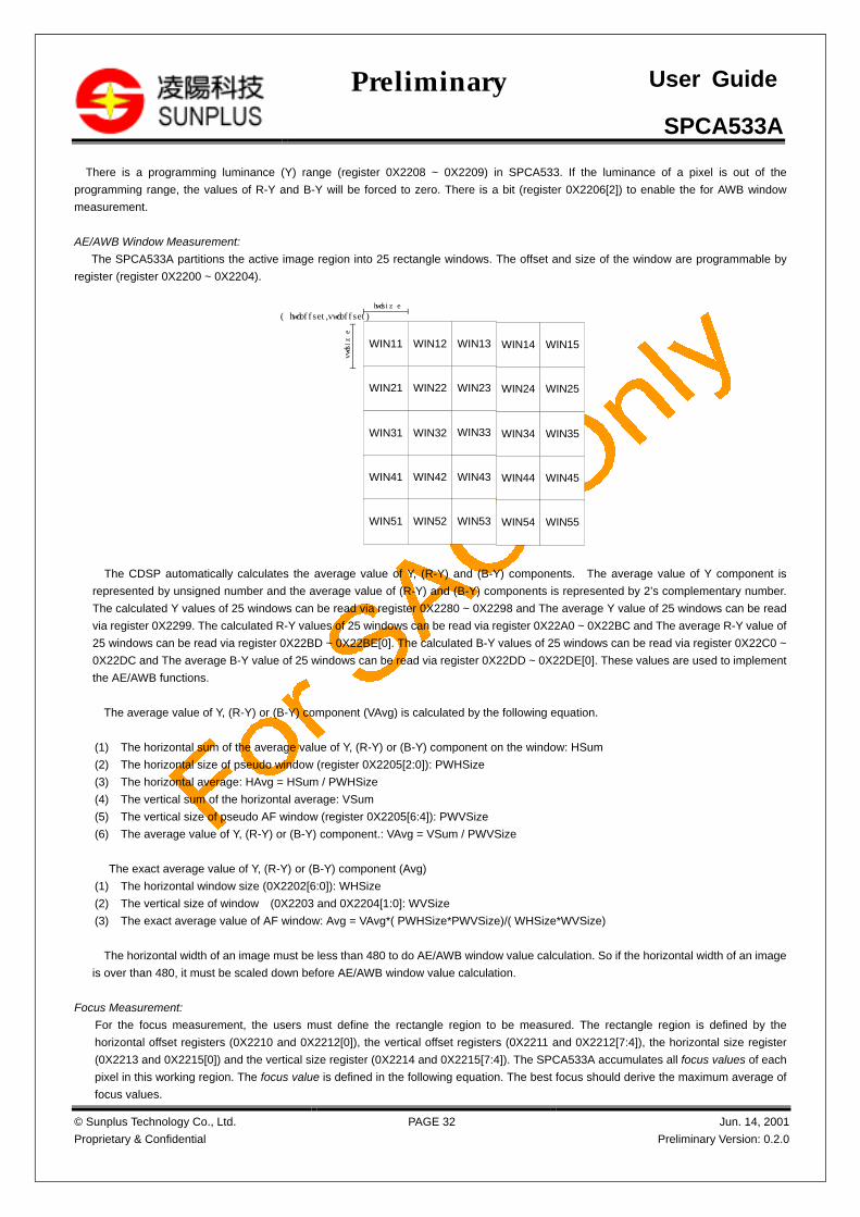
SPCA533A
© Sunplus Technology Co., Ltd.
Proprietary & Confidential
PAGE 32 Jun. 14, 2001
Preliminary Version: 0.2.0
Preliminary User Guide
There is a programming luminance (Y) range (register 0X2208 ~ 0X2209) in SPCA533. If the luminance of a pixel is out of the
programming range, the values of R-Y and B-Y will be forced to zero. There is a bit (register 0X2206[2]) to enable the for AWB window
measurement.
AE/AWB Window Measurement:
The SPCA533A partitions the active image region into 25 rectangle windows. The offset and size of the window are programmable by
register (register 0X2200 ~ 0X2204).
WIN11 WIN12 WIN13 WIN14 WIN15
WIN21 WIN22 WIN23 WIN24 WIN25
WIN31 WIN32 WIN33 WIN34 WIN35
WIN41 WIN42 WIN43 WIN44 WIN45
WIN51 WIN52 WIN53 WIN54 WIN55
hwdsize
vwdsize
(hwdoffset,vwdoffset)
The CDSP automatically calculates the average value of Y, (R-Y) and (B-Y) components. The average value of Y component is
represented by unsigned number and the average value of (R-Y) and (B-Y) components is represented by 2’s complementary number.
The calculated Y values of 25 windows can be read via register 0X2280 ~ 0X2298 and The average Y value of 25 windows can be read
via register 0X2299. The calculated R-Y values of 25 windows can be read via register 0X22A0 ~ 0X22BC and The average R-Y value of
25 windows can be read via register 0X22BD ~ 0X22BE[0]. The calculated B-Y values of 25 windows can be read via register 0X22C0 ~
0X22DC and The average B-Y value of 25 windows can be read via register 0X22DD ~ 0X22DE[0]. These values are used to implement
the AE/AWB functions.
The average value of Y, (R-Y) or (B-Y) component (VAvg) is calculated by the following equation.
(1) The horizontal sum of the average value of Y, (R-Y) or (B-Y) component on the window: HSum
(2) The horizontal size of pseudo window (register 0X2205[2:0]): PWHSize
(3) The horizontal average: HAvg = HSum / PWHSize
(4) The vertical sum of the horizontal average: VSum
(5) The vertical size of pseudo AF window (register 0X2205[6:4]): PWVSize
(6) The average value of Y, (R-Y) or (B-Y) component.: VAvg = VSum / PWVSize
The exact average value of Y, (R-Y) or (B-Y) component (Avg)
(1) The horizontal window size (0X2202[6:0]): WHSize
(2) The vertical size of window (0X2203 and 0X2204[1:0]: WVSize
(3) The exact average value of AF window: Avg = VAvg*( PWHSize*PWVSize)/( WHSize*WVSize)
The horizontal width of an image must be less than 480 to do AE/AWB window value calculation. So if the horizontal width of an image
is over than 480, it must be scaled down before AE/AWB window value calculation.
Focus Measurement:
For the focus measurement, the users must define the rectangle region to be measured. The rectangle region is defined by the
horizontal offset registers (0X2210 and 0X2212[0]), the vertical offset registers (0X2211 and 0X2212[7:4]), the horizontal size register
(0X2213 and 0X2215[0]) and the vertical size register (0X2214 and 0X2215[7:4]). The SPCA533A accumulates all focus values of each
pixel in this working region. The focus value is defined in the following equation. The best focus should derive the maximum average of
focus values.
SPCA533A
© Sunplus Technology Co., Ltd.
Proprietary & Confidential
PAGE 33 Jun. 14, 2001
Preliminary Version: 0.2.0
Preliminary User Guide
A1 A2 A3
A4 A5 A6
A7 A8 A9
Focus value of pixel A5:
FV = |(A7+A8+A9)-(A1+A2+A3)| + |(A3+A6+9)-(A1+A4+A7)|
The average value of AF window (VFvAvg) can be read from register (0X2117 and 0X2118[4:0]). The value is represented by 2’s
complementary number that is calculated by the following equation.
(7) The horizontal sum of focus value on the AF window: HFvSum
(8) The horizontal size of pseudo AF window (register 0X2216[2:0]): PAFWHSize
(9) The horizontal average of focus value: HFvAvg = HFvSum / PAFWHSize
(10) The vertical sum of the horizontal average of focus value: VFvSum
(11) The vertical size of pseudo AF window (register 0X2216[7:4]): PAFWVSize
(12) The vertical average of focus value (0X2117 and 0X2118[4:0]).: VFvAvg = VFvSum / PAFWVSize
The exact average value of AF window (AFAvg)
(4) The horizontal size of AF window (0X2213 and 0X2215[0]): AFWHSize
(5) The vertical size of AF window (0X2214 and 0X2215[7:4]): AFWVSize
(6) The exact average value of AF window: AFAvg = VFvAvg*( PAFWHSize* PAFWVSize)/( AFWHSize* AFWVSize)
The horizontal width of an image must be less than 480 to do AF window value calculation. So if the horizontal width of an image is
over than 480, it must be scaled down before AF window value calculation.
1.4 DMA controller
The DMA controller in the SPCA533A is in charge of moving data between different modules. It is very flexible and fast.
The DMA data transfer can be performed among six different modules. They are SDRAM, SRAM (address 0x1000~0x1FFF), 1K audio
buffer, USB bulk-pipe buffer, the storage media and the CPU PIO. Before each DMA data transfer, the source and destination of the DMA
transfer must be assigned first (register 0x2301).
The CPU PIO is a data port at register 0x2300, through which the CPU can access the internal FIFO of the DMA controller. There are
4-byte FIFO in the DMA controller. The size is adjustable via register 0x2304[3:2]. When the CPU PIO is set to be the source of a DMA
transfer, the CPU must check the DMAFULL flag (register 0x23A0[3]). No more data can be written in to the DMA controller if this flag is high.
On the other hand, if the CPU PIO is set to be the destination of a DMA transfer, the CPU must check the DMAEMPTY flag (register
0x23A0[4]). No more data can be read from the DMA controller if the flag is high. These flags need to be checked only when the CPU PIO is
involved. DMA transfer among other modules are automatically handled by hardware. The firmware need only check the DMA complete flag
(register 0x23C0).
It is prohibited to set the source and the destination of a DMA transfer to the same module. To move data to different locations inside the
SDRAM, the SPCA533A provide another type of DMA control flow, which is discussed in the SDRAM controller section.
1.4.1 Direction of the DMA
The following table lists all the combination of different DMA sources and targets. All these DMA operations are performed in all camera
operation modes, except the PC-camera mode. In the PC-camera mode the data flow is manipulated by hardware, the firmware needs only
initializing the data path.

SPCA533A
© Sunplus Technology Co., Ltd.
Proprietary & Confidential
PAGE 34 Jun. 14, 2001
Preliminary Version: 0.2.0
Preliminary User Guide
Source
(data provider)
Destination
(data consumer)
Function description
DRAM CPUPIO For internal diagnostic
DRAM SRAM Copy data from the DRAM to the SRAM Useful in FAT manipulation.
DRAM Storage media Save the image/audio data in the DRAM to the Storage media.
DRAM AUDIO Playback an audio file that is already exists in the DRAM.
DRAM USB (Bulk) Upload data from the DRAM to the PC
CPU PIO Any The CPU can prepare random data to be moved to the designated destination.
SRAM CPUPIO This mode is redundant, because the CPU can directly access the SRAM.
DRAM Copy data from the SRAM to the DRAM. Useful in the FAT manipulation.
Storage media Copy data from the SRAM to the storage media. Useful when the file header is constructed
in the SRAM.
AUDIO Playback audio file from the SRAM.
USB (Bulk) Upload SRAM data to the PC. If the ECC correction is implemented in the firmware while
uploading files to the PC, the data is first moved from the storage media to SRAM. Then the
ECC correction is done in the SRAM. Finally, the corrected data is sent to the PC from the
SRAM to the USB. Basically, any DMA data transfer can be divided into two DMA data
transfer with the SRAM as the bridge, so that the CPU has the opportunity to modify the
data in the midway.
Storage media CPUPIO For internal diagnostic
DRAM Fetch an image/audio file and stores in the DRAM for playback.
Load the FAT from the storage media to the DRAM for further processing.
SRAM To speed up the playback tasks, the header of the image file (or audio file) is loaded from
the storage media to the SRAM first. And the header parsing is done in the SRAM. After the
size of the file is determined, the remaining of the file is loaded to the DRAM.
AUDIO Not useful. Normally, the header of the audio file must be stripped by the firmware before
playback. However, it is possible to playback the audio file directly from the storage media
when the file is a raw PCM data file.
USB (Bulk) Upload captured image/audio file to the PC.
AUDIO CPUPIO Internal diagnostic only
DRAM Record the audio data to the DRAM. This is used in the Video Clip and in the audio
recording.
SRAM Record short sound file only. The size must be under 4K bytes.
Storage media Not practical. The access speed of the storage media might cause the recording to pause.
USB (Bulk) Used in the PC-camera mode. The SPCA533A can acts as a PC-camera with a microphone
input.
USB(Bulk) CPUPIO Internal diagnostic only
DRAM Download data from the PC to the DRAM. Might be used in the ISP function, in which the
complete firmware is downloaded in to the DRAM first.
SRAM Download data from the PC to the DRAM. Might be used in the ISP function, in which the
new firmware is partitioned to blocks of 4K-byte. Each time, the 4K-byte of the ROM code is
updated.
Storage media Download image/audio file from the PC to the storage media.
Audio The SPCA533A can act as an USB speaker in this mode. This is not practical in real
application, but very useful while developing the sound data base.
SPCA533A
© Sunplus Technology Co., Ltd.
Proprietary & Confidential
PAGE 35 Jun. 14, 2001
Preliminary Version: 0.2.0
Preliminary User Guide
1.4.2 Page size adjustment of the DMA
The maximum size of each DMA transfer is limited to 1K-byte. The size is programmable via register 0x2302, 0x2303[1:0]. If the
destination of the DMA transfer is the storage media and the DMA size is not aligned to the page size of that storage media, the SPCA533A
can automatically padding 0’s to make the last data transfer a complete page. This is done through enabling the padding function of the
DMA controller. (register 0x2304[1]). On the other hand, if the source of a DMA transfer is the storage media and the DMA size is not aligned
to the page size, the DMA controller will issue dummy read to the storage media but the data (of the dummy read) is never sent to the
destination. When there are padding 0’s or dummy reads, the DMA complete flag will not be high until all the padding and dummy reads are
done. The page size refers to the register 0x24A3.
1.4.3 Matching pattern in DMA
The DMA controller provides a pattern-search function during a DMA data transfer. The pattern-search is done by peeping the data
during data transfer. After a DMA transfer is completed, the DMA controller will report the number of matched pattern (register 0x2313) and
the location of the first matched pattern in current DMA transfer (register 0x23A1, 0X23A2[1:0]). This function is useful to help the firmware
searching the empty clusters in the FAT. Normally, an empty cluster is represented by a special code in the FAT. The SPCA533A supports
both 12-bit and 16-bit pattern search, which correspond FAT12 and FAT16 system. The pattern to be searched is programmable via register
0x2311 and 0x2312.
For 16-bit pattern, register 0x2311 is the low-byte pattern and register 0d2312 is the high-byte pattern. For 12-bit pattern, register 0x2311
is the low-byte pattern and register 0x2312[7:4] is neglected. Byte-order bit (register 0x2310[4]) indicates whether the transfer sequence is
high-byte first or low-byte first.
The following is an example of the pattern-search.
Transfer Order: 0 1 2 3 4 5 6 7 8 9 10 11 12
Data: { 00 04 0F 01 04 05 01 0F 08 01 0F 0B 0C }
Assume a 16-bit pattern of 0x0F01 is to be searched and the data sequence is low-byte first, the DMA controller will report the first
match at location 7 and the matched count is 2. Byte6 and Byte7 form a matched pair while byte 9 and byte 10 form another. Note that byte 2
and byte 3 do not match the pattern since the sequence is reversed. A match flag in register 0x23A2[2] is asserted right after the pattern
matches. The number of the matched count is in register 0x23A2[1:0] and register 0x23A1.
An example of manipulating the FAT is shown in the following diagram.

SPCA533A
© Sunplus Technology Co., Ltd.
Proprietary & Confidential
PAGE 36 Jun. 14, 2001
Preliminary Version: 0.2.0
Preliminary User Guide
Prepare FAT in DRAM
1.DMA setting : size : 1K (if FAT data >= 1K)2.DRAM start address , SRAM start address2.trigger DMA : set reg. 0x23B0.
DMA complete? (polling reg.0x23C0)
FAT matching setting:1. select fatmode[1:0] (reg.0x2310[1:0] ,fat16 or fat12)2. low byte first matching (set 0x2310[4])3. fill the searching code in reg.0x2311, 0x2312. (0x000 for fat12, 0x0000 for fat16)
Set the DRAM start address tothe 1st cluster content in FAT
searching code occurs in DMA cycle ?( 0x23A2 [2] == 1?)
f ind the f i rs t matched codeposition in current DMA cycle( { 0x23A2 [1:0] , 0x23A1 } )and fill the next cluster number inthe coreesponding SRAM
Cluster enough ?
Last FAT block?
Finish Space is not enough
find the next matched code in 1KSRAM if hit count > 1and fill the next cluster number inthe coreesponding SRAM
redundant hit count in1K SRAM?
(check register 0x2313)
Cluster enough ?
DMA setting : (source: DRAM, destination:CPU 4K buffer)
YN
Y N
Y
N
N
Y
N
Y
Y
N
SRAM to DRAM DMA
SRAM to DRAMDMA

SPCA533A
© Sunplus Technology Co., Ltd.
Proprietary & Confidential
PAGE 37 Jun. 14, 2001
Preliminary Version: 0.2.0
Preliminary User Guide
1.4.4 DMA control flow
To start a DMA data transfer, the starting address of the related modules must be set before the DMA operation is triggered. The
following flow charts shows the related register setting and checking sequence. However, if CPU PIO is the source or the destination of DMA,
the sequence is different from the flow chart. The sequence is right after the DMA flow chart.
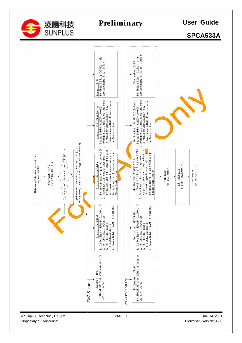
SPCA533A
© Sunplus Technology Co., Ltd.
Proprietary & Confidential
PAGE 38 Jun. 14, 2001
Preliminary Version: 0.2.0
Preliminary User Guide
trigger DMA
set 0x23B0[0] = 1
polling DMAcmp
(until 0x23C0[0] == 1)
Clear DMAcmp
set 0x23C0[0] = 0
Source : DRAM
Set DRAM DMA start address via register
0x2750 ~ 0x2752
Source : 4K SRAM
1. Disable high-4K SRAM (0x2C00[1]=0)
2. Set DMA mode (0x2C11=2)
3. Fill initial address
(0x2C12,0x2C13[3:0])
4. Enable high-4K SRAM (0x2C00[1]=1)
Source : Storage Media
1. Set storage media type (register 0x2400)
2. According to different storage media
type, configure the storage media such
as transmiting mode, address and size
before triggering . Please refer to the
Storage Media section.
Source : 1K AUDIO Buffer
1. Set AuBMode (0x2605) to 0x05
2. Configure audio related registers such
as AuStereo, ADPCMCodcEn, etc.,
before triggering DMA. Please refer to
the Audio section.
Source : USB
Set DMAUSBSrc (0x2510) to the
corresponding Bulk-out buffer.
Destination : DRAM
Set DRAM DMA start address via register
0x2750 ~ 0x2752
Destination : 4K SRAM
1. Disable high-4K SRAM (0x2C00[1]=0)
2. Set DMA mode (0x2C11=2)
3. Fill initial address
(0x2C12, 0x2C13[3:0])
4. Enable high-4K SRAM (0x2C00[1]=1)
Destination : Storage Media
1. Set storage media type (register 0x2400)
2. According to different storage media
type, configure the storage media such
as transmiting mode, address and size
before triggering . Please refer to the
Storage Media section.
Destination : 1K AUDIO Buffer
1. Set AuBMode (0x2605) to 0x06
2. Configure audio related registers such
as AuStereo, ADPCMCodcEn, etc.,
before triggering DMA. Please refer to
the Audio section.
Destination : USB
Set DMAUSBDst (0x2511) to the
corresponding Bulk-in/Int-in buffer
DMA source/destination setting
(register 0x2301)
DMA transfer size
(0x2302, 0x2303[1:0])
padding function enable (register 0x2304[1])
storage memory page size setting (register 0x24A3)
storage media is one client of DMA
DMA Source
DMA Destination
YN

SPCA533A
© Sunplus Technology Co., Ltd.
Proprietary & Confidential
PAGE 39 Jun. 14, 2001
Preliminary Version: 0.2.0
Preliminary User Guide
DMA CPU PIO Write Flow
DMA destination setting(register 0x2301[6:4])source : CPU PIO (set register 0x2301[2:0]=5)
trigger DMAset 0x23B0[0] = 1
Clear DMAcmpset 0x23C0[0] = 0
DMA transfer size(0x2302, 0x2303[1:0])
padding function enable (register 0x2304[1])storage memory page size setting (register 0x24A3)
storage media is one client of DMA
N
Y
DMA destination setting
DMA buffer size = 4(0x2304[3:2] = 4, default)
polling DMAempty(until 0x23A0[4] == 1)
CPU write DMA data port (register 0x2300)4 times once
polling DMAcmp(register 0x23C0[0])
01
DMA source setting(register 0x2301[2:0])destination : CPU PIO (set register 0x2301[6:4]=5)
trigger DMAset 0x23B0[0] = 1
Clear DMAcmpset 0x23C0[0] = 0
DMA transfer size(0x2302, 0x2303[1:0])
padding function enable (register 0x2304[1])storage memory page size setting (register 0x24A3)
storage media is one client of DMA
N
Y
DMA source setting
DMA buffer size = 4(0x2304[3:2] = 4, default)
polling DMAfull(until 0x23A0[3] == 1)
CPU read DMA data port (register 0x2300) 4 timesonce
polling DMAcmp(register 0x23C0[0])
01
DMA CPU PIO Read Flow
1.5 Storage media
Except from the SDRAM, the SPCA533A supports 5 types of storage media, which are controlled by the flash memory controller. There
are two accessing modes to read/write the flash memory. One is the PIO mode and the other is the DMA mode. The storage media
interfaces are listed below
1. Nand-gate flash memory interface, this interface is also applicable to the SmartMedia.
2. The interface to the CompactFlash cards. It supports the PC card memory mode and the true IDE mode. The true IDE mode also applies
to the IDE CDRW such that the SPCA533A can save/restore data to/from the IDE CDRW.
3. SPI interface to the SPI-type serial flash memory with mode 0 and mode 3 supported. This interface also applies to the SPI mode of

SPCA533A
© Sunplus Technology Co., Ltd.
Proprietary & Confidential
PAGE 40 Jun. 14, 2001
Preliminary Version: 0.2.0
Preliminary User Guide
MultiMediaCard.
4. The serial interface to the NextFlash serial flash memory.
5. The interface to the SD memory cards.
Although most of the storage media have various operation modes, the SPCA533A supports only SPI mode for the MultiMediaCard,
supports PC card memory mode and true IDE mode for the CompactFlash memory cards, and supports only SD mode for the SD memory
cards. The SPCA533A has 30 dedicated pins for storage media interface. The pin definitions are different according to the type of the
selected storage media.
1.5.1 PIO mode and DMA mode
In PIO mode, the SPCA533A reads or writes the corresponding registers for reading/writing storage media byte by byte. Thus the data
throughput is limited by the CPU speed. While in DMA mode, the built-in flash DMA controllers can read/write data automatically.
When writing a page of data to the storage media, write data to the DMA source first and then start the DMA controller to move data from
the DMA source to the storage media. When reading a page of data from the storage media, start the DMA controller to move data from
storage media to the DMA destination. Reference to the DMA section to see the setting of DMA controller. The difference of PIO and DMA
mode is the data transferring but not command or address setting. To communicate with different storage media, the protocol is made by the
storage media interface module but not DMA controller. In the next section, the PIO and DMA mode for Nand-gate flash is described below.
Actually, the setting of DMA mode in other storage media, such as SmartMediaCard, SPI flash, SD memory cards and NextFlash is similar.
1.5.2 Nand-gate flash memory and SmartMediaCard
The interfaces of the Nand-gate flash and the SmartMedia memory card are almost alike except that there is an additional card detection
function in the interface of SmartMedia memory card. Thus, we only consider the Nand-type flash memory.
The SPCA533A supports Nand-gate flash memory in two ways. The first one is PIO mode and the other is DMA mode. In PIO mode, the
CPU write command, address and data to the Nand-gate flash memory via register 0X2420. The CPU also read data and the status byte
from the Nand-gate flash memory via register 0X2420. In addition, it also can read the status pin from register 0x2424.
In DMA mode, the CPU write command and address to the Nand-gate flash memory via register 0X2420. It reads the status byte via
register 0x2420. For data read and write, the CPU does not need to read/write byte by byte. Instead it triggers the built-in DMA controller.
Note that the card detection interrupt function of SmartMedia memory cards interface can be enabled by the fmgpio interrupt function.
Setting register 0x2410 bit5 to 1 for rising edge interrupt, register 0x2414 bit5 for falling edge interrupt and the interrupt status is reported in
the register 0x2418 bit5. The following flowcharts described the details of control flow in PIO mode and in DMA mode.
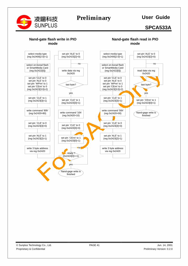
SPCA533A
© Sunplus Technology Co., Ltd.
Proprietary & Confidential
PAGE 41 Jun. 14, 2001
Preliminary Version: 0.2.0
Preliminary User Guide
Nand-gate flash read in PIOmode
Nand-gate flash write in PIOmode
set pin 'CLE' to 0set pin 'ALE' to 0
set pin `WPnn' to 1set pin 'CEnn' to 0
(reg 0x2423[3:0]=2)
last byte?
yes
Nand-gage write isfinished
select media type(reg 0x2400[2:0]=1)
select on-borad flashor SmartMedia Card
(reg 0x2422[0])
set pin `CLE' to 1(reg 0x2423[3]=1)
write command '80h'(reg 0x2420=80)
set pin `CLE' to 0(reg 0x2423[3]=0)
no
write data via reg0x2420
set pin `CLE' to 1(reg 0x2423[3]=1)
write command '10h'(reg 0x2420=10)
set pin `CLE' to 0(reg 0x2423[3]=0)
set pin `CEnn' to 1(reg 0x2423[0]=1)
set pin 'ALE' to 1(reg 0x2423[2]=1)
write 3 byte addressvia reg 0x2420
set pin 'ALE' to 0(reg 0x2423[2]=0)
set pin 'CLE' to 0set pin 'ALE' to 0
set pin `WPnn' to 1set pin 'CEnn' to 0
(reg 0x2423[3:0]=2)
last byte?
yes
Nand-gage write isfinished
select media type(reg 0x2400[2:0]=1)
select on-borad flashor SmartMedia Card
(reg 0x2422[0])
set pin `CLE' to 1(reg 0x2423[3]=1)
write command '00h'(reg 0x2420=00)
set pin `CLE' to 0(reg 0x2423[3]=0)
no
read data via reg0x2420
set pin `CEnn' to 1(reg 0x2423[0]=1)
set pin 'ALE' to 1(reg 0x2423[2]=1)
write 3 byte addressvia reg 0x2420
set pin 'ALE' to 0(reg 0x2423[2]=0)
ready ?(0x2424[0]==1)
no
yes

SPCA533A
© Sunplus Technology Co., Ltd.
Proprietary & Confidential
PAGE 42 Jun. 14, 2001
Preliminary Version: 0.2.0
Preliminary User Guide
Nand-gate flash read in DMAmode
Nand-gate flash write in DMAmode
set pin 'CLE' to 0set pin 'ALE' to 0
set pin `WPnn' to 1set pin 'CEnn' to 0
(reg 0x2423[3:0]=2)
DMA complete?(0x23C0[0])
yes
Nand-gage write isfinished
select media type(reg 0x2400[2:0]=1)
select on-borad flashor SmartMedia Card
(reg 0x2422[0])
set pin `CLE' to 1(reg 0x2423[3]=1)
write command '80h'(reg 0x2420=80)
set pin `CLE' to 0(reg 0x2423[3]=0)
(reg 0x2301[6:4]=2)(program reg 0xx2301[2:0],
0x2302, 0x2304[1])trigger DMA 23B0[0] = 1
set pin `CLE' to 1(reg 0x2423[3]=1)
write command '10h'(reg 0x2420=10)
set pin `CLE' to 0(reg 0x2423[3]=0)
set pin `CEnn' to 1(reg 0x2423[0]=1)
set pin 'ALE' to 1(reg 0x2423[2]=1)
write 3 byte addressvia reg 0x2420
set pin 'ALE' to 0(reg 0x2423[2]=0)
set pin 'CLE' to 0set pin 'ALE' to 0
set pin `WPnn' to 1set pin 'CEnn' to 0
(reg 0x2423[3:0]=2)
yes
Nand-gage write isfinished
select media type(reg 0x2400[2:0]=1)
select on-borad flashor SmartMedia Card
(reg 0x2422[0])
set pin `CLE' to 1(reg 0x2423[3]=1)
write command '00h'(reg 0x2420=00)
set pin `CLE' to 0(reg 0x2423[3]=0)
set pin `CEnn' to 1(reg 0x2423[0]=1)
set pin 'ALE' to 1(reg 0x2423[2]=1)
write 3 byte addressvia reg 0x2420
set pin 'ALE' to 0(reg 0x2423[2]=0)
ready ?(0x2424[0]==1)
no
yes
no
DMA complete?(0x23C0[0])
(reg 0x2301[2:0]=2)(program reg 0x2301[6:4],
0x2302, 0x2304[1])trigger DMA 23B0[0] = 1
no
Note that for operating in DMA mode, the active time and recovery time of read/write pulse can be programmed via register 0x2421. See
the diagram shown below.
active
recovery
WEnn or REnn
1.5.3 CompactFlash cards interface
The CompactFlash cards interface of SPAC533 supports PC-card memory mode and true IDE mode. The true IDE mode also applies to
the IDE CDRW machine. Both in memory mode and true IDE mode, the ATA standard is applied and it defines a set of registers. In the PC-
card memory mode, ATA registers and memory are selected by 1 chip select pins, 1 register pin and 11 address pins. While in the true IDE
mode, ATA registers are selected by 2 chip select pins and 3 address pins. Thus, the firmware must program register 0x2434 bit2 first to
select the memory mode or the true IDE mode. Then, the firmware must program register 0x2436 for chip select pins, register 0x2439 for
register pin, and registers 0x2432~0x2433 for address pins. Registers 0x2430~0x2431 are the data port for the data transfer. The

SPCA533A
© Sunplus Technology Co., Ltd.
Proprietary & Confidential
PAGE 43 Jun. 14, 2001
Preliminary Version: 0.2.0
Preliminary User Guide
SPCA533A supports the byte access and word access in the true IDE mode while only supports the byte access in the memory mode. The
firmware can set register 0X2434 to determine whether to perform a 16-bit or 8-bit data transfer. Due to the different operating modes of
CompactFlash cards, the specification of read/write pulse may be different. The firmware can set register 0X2435 to configure the active
time and recovery time of the read/write pulse. The detailed information about how to control the ATA device, including the ATA command
sets, could be referenced in ATA specification. The following flowchart shows how to control the CompactFlash interface in the SPCA533.
The interrupt generated from the CompactFlash card is also routed into the SPCA533. The interrupt status can be polled by reading register
0X24C0 bit 0.
CompactFlashwrite
select CF mode(reg 0x2434[2])
select byte access orword access
(reg 0x2434[0])
set read/write pulsewidth
(reg 0x2435[3:0])
set chip select(reg 0x2436[1:0])
set pin 'REG/' ifmemory mode(reg 0x2439[0])
CompactFlashread
select CF mode(reg 0x2434[2])
select byte access orword access
(reg 0x2434[0])
set read/write pulsewidth
(reg 0x2435[3:0])
set chip select(reg 0x2436[1:0])
set pin 'REG/' ifmemory mode(reg 0x2439[0])
set address(reg 0x2432~0x2433)
set pre-fetch(reg 0x2434[1]=1)
read data(reg 0x2430~0x2431)
ready?(0x243b[0]==1)
YES
last data?
NO
NO
disable pre-fetch(reg 0x2434[1]=0)
read data(reg 0x2430~0x2431)
finish
ready?(0x243b[0]==1)
YES
finish
last data?
set address(reg 0x2432~0x2433)
write data(reg 0x2430~0x2431)
YES
NO
NO
1.5.4 SPI interface to the Serial flash memory
The SPCA533A supports an SPI serial interface to access the SPI-type serial flash memory. Both SPI mode 0 and SPI mode 3 are
supported. The SPI interface also enables the SPCA533A to access the MultiMediaCard operating in SPI mode. The serial clock frequency
is adjustable from 12 MHz to 200KHz. The CPU writes data to the serial flash memory via the TXport (register 0x2440) and read data from
the flash memory via the RXport and PRXport. Reading data from the PRXport will invoke a sequence of serial clocks to pre-fetch the next
byte of data. Reading data from the RXport merely gets the data that is already received and latched in the SPCA533. Each read sequence
starts with a dummy read to the PRXport, followed by multiple read from the PRXport, and finally end up with a read to the RXport. Note that
the data read by the first dummy read to the PRXport should be discarded. Each time before the CPU write to the TXport or read from the
PRXport, the CPU must wait until the SPI interface is ready. This could be achieved by polling the status bit (FMSIbusy, register 0X244b bit 0)
each time before read or write. The following diagram shows the control flow of the SPI interface.
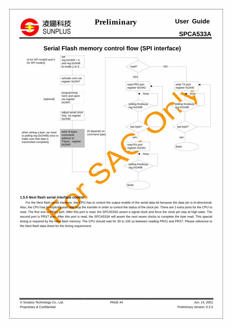
SPCA533A
© Sunplus Technology Co., Ltd.
Proprietary & Confidential
PAGE 44 Jun. 14, 2001
Preliminary Version: 0.2.0
Preliminary User Guide
(4 for SPI mode0 and 5for SPI mode3)
activate csnn viaregister 0x2447
programmingrstnn and wpnnvia register0x2447
(optional)
adjust serail clockfreq. via register0x2446
write N bytescommand/address toTXport , register0x2440
(N depends oncommand type)
read?
YES
read PRX portregister 0x2442
polling fmsibusyreg 0x244B
busy
last byte?
yes
read RX portregister 0x2441
finish
NO
write TX portregister 0x2440
busy
last byte?
yes
finish
Serial Flash memory control flow (SPI interface)setreg 0x2400 = 4and reg 0x2448to mode 1 or 3
when wirting a byte, we needto polling reg (0x244B) once tomake sure that data istransmitted completely
polling fmsibusyreg 0x244B
polling fmsibusyreg 0x244B
busy
1.5.5 Next flash serial interface control
For the Next flash serial interface, the CPU has to control the output enable of the serial data bit because the data pin is bi-directional.
Also, the CPU has to explicitly start and stop the transfer in order to control the status of the clock pin. There are 2 extra ports for the CPU to
read. The first one is PRX1 port. After this port is read, the SPCA533A assert a signal clock and force the clock pin stay at high state. The
second port is PRX7 port. After this port is read, the SPCA533A will assert the next seven clocks to complete the byte read. This special
timing is required by the Next flash memory. The CPU should wait for 30 to 100 us between reading PRX1 and PRX7. Please reference to
the Next flash data sheet for the timing requirement.

SPCA533A
© Sunplus Technology Co., Ltd.
Proprietary & Confidential
PAGE 45 Jun. 14, 2001
Preliminary Version: 0.2.0
Preliminary User Guide
set reg 0x2440 = 5Next flash mode
set serial clockfrequency
(reg 0x2446)(optional)
write 3 bytes address/command
write 4 reserved bytesans trun off the ouputenable(reg 0x2447)
read PRX (0x2442)
read RX port (0x2441)
read RX1 port(0x2443)
read RX7 port(0x2444)
READY?(9999H)
finish
write?YES
YES
write TX port (0x2440)
lastwrite?
finish
NO
no
NO
read PRX port(0x2442)
(dummy read)
read PRX port(0x2442)
(dummy read)
last read? no
finish
Next Flash serail interface control flow
turn on output enable(0x2447)
write reg 0x244A=2 to stop data transfer
yes
read PRX port(0x2441)
without trigger
yes
turn on output enableof the data pin
(reg 0x2447) and write0x244A=1 to start
transferwake up
1st byte out
2nd byte out
when wirting a byte, we need topolling reg (0x244B) once tomake sure that data is transmitted
completely
tRP
polling0x244B
polling0x244B
ignore the 1st bytepolling0x244B
polling0x244B
write reg 0x244A=2 to stop data transfer
yes
polling0x244B
read RX port (0x2441)
polling0x244B
1.5.6 SD memory cards interface
The SD memory interface provides the SPAC533 to access the SD (Security Digital) memory cards. The serial clock frequency is
adjustable from 24 MHz to 375KHz by setting register 0x2451 bit0~1. This data block length is from 1 byte to 1023 bytes by setting register
0x2455 and 0x2456. Command is sent via command buffer (0x245B – 0x245F) and response is received via response buffer (0x2460 –
0x2465). The register ‘RspBufRdy’ is the status report of that response buffer is full. Thus, the firmware gets the permission to receive
response only when ‘RspBufRdy’ is 1. Setting register ‘RxRsp’ to 1 will trigger the controller to wait response and a response wait timer is
applied. Thus, the firmware must set the response length (0x2451 bit3) and the response time (0x2457) first. If the response time is passed
and there is no response, the timeout condition will report (0x2453 bit 6). The firmware must abort waiting response. Note that the CRC7
code calculation is applied for sending command and receiving response, and setting register SDCRCrst to 1 will clear the CRC7 register.
For writing data, the firmware must decide the data block length (0x2455 and 0x2456) and data bus width (0x2451 bit2). Like the
command and response, sending and receiving data is also via data TX (0x2459) and RX (0x245A) buffer. The registers ‘DataBufEmpty’
and ’DataBufFull’ will indicate that data is sent or that data buffer is full. It is needed to get the CRC check result of the card after data is
transmitted completely by setting register ‘RxCardCRC’ (0x2452 bit 4). The whole writing procedure is completed only after the card status is
not busy (0x2453 bit5).
For reading data, first step is setting register ‘RxData’ to 1 for triggering interface controller to wait data. CRC16 code is applied for
writing and reading data. The firmware must check the CRC16 code calculated by SPAC533. Register ‘SDCRCrst’ can also clear the CRC16
registers.
The card detection of SD memory card is also supported by the fmgpio interrupt function. If the firmware enables the fmgpio2 interrupt

SPCA533A
© Sunplus Technology Co., Ltd.
Proprietary & Confidential
PAGE 46 Jun. 14, 2001
Preliminary Version: 0.2.0
Preliminary User Guide
(0x2410 bit2 for rising edge interrupt enable and 0x2414 bit2 for falling edge interrupt enable), the detection of SD memory card will generate
an interrupt request to the CPU and it will be reported in the register 0x2418 bit 2.
The dummy clock is applied when the SD memory card needs the dummy clock to complete its operating. Setting register ‘TxDummy’ to
1 will generate 8 clock cycles. The firmware can get the state status by reading the register ‘SDState’. Note that the SD software reset can
reset the SD memory interface.
For more details of the SD memory card, including the command, response and register set, please refer to the specification of the SD
memory card. The following flowchart will describe how the control the command/response and read/write data.

SPCA533A
© Sunplus Technology Co., Ltd.
Proprietary & Confidential
PAGE 47 Jun. 14, 2001
Preliminary Version: 0.2.0
Preliminary User Guide
SD flash command and response
select clock frequencyto the SD memory(reg 0x2451[1:0])
select response length(reg 0x2455 and
0x2456)
set response wait time(reg 0x2457)
reset CRC register(reg 0x2450[1]=1)
start receiving response(reg 0x2452[1]=1)
respopnse bufferfull or timeout?
(0x2453[1]==1 or0x2453[6]==1)
read 5 response valuefrom RespBuf1 to
RespBuf5(reg 0x2460 to 0x2464)
last byte?
response in(0x2453[1]=1)
YES
timeout(0x2453[6]==1)
NONO
finish(response success)
YES
send dummy clock(reg 0x2453[5])
check responseCRC7
CORRECT
finish(response fail)
INCORRECT
set command bufferCmdBuf1 to CmdBuf5
(reg 0x245B to 0x245F)
start transmittingcommand
(set reg 0x2452 [0] = 1)
idle state?(reg 0x2454 ==0)
NO
YES
read responseRespBuf6
(reg 0x2465)
response buffer full?(reg 0x2453[1]==1)
select response type(reg 0x2451[3])

SPCA533A
© Sunplus Technology Co., Ltd.
Proprietary & Confidential
PAGE 48 Jun. 14, 2001
Preliminary Version: 0.2.0
Preliminary User Guide
select data bus width(reg 0x2451[2])
select clock frequencyto the SD memory(reg 0x2451[1:0])
select data blocklength
(reg 0x2455, 0x2456)
reset CRC register(reg 0x2450[1]=1)
start transmit data(set reg 0x2452[2] = 1)
write data butter (tx)(reg 0x2459)
data bufferready?
(0x2453[2]==1)
YES
NO
last byte?
NO
SD flash write data
NO YES
start receive CRCresult of the card(reg 0x2452[4]=1)
idle state?(0x2454==0)
NO
YES
send dummy clock(reg 0x2452[5])
card busy?(0x2453[5]==0)
YES
NO
finish
YES
start transmitcommand
.
.
.
trasnsmit command isfinished
idle state?(reg 0x2454==0)
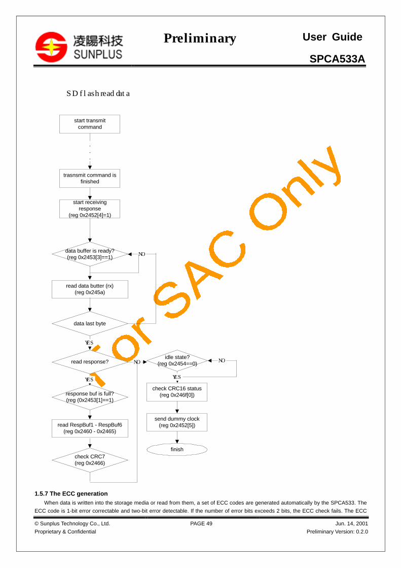
SPCA533A
© Sunplus Technology Co., Ltd.
Proprietary & Confidential
PAGE 49 Jun. 14, 2001
Preliminary Version: 0.2.0
Preliminary User Guide
SD flash read data
start transmitcommand
.
.
.
trasnsmit command isfinished
start receivingresponse
(reg 0x2452[4]=1)
read data butter (rx)(reg 0x245a)
data last byte
NO
YES
check CRC16 status(reg 0x246f[0])
finish
send dummy clock(reg 0x2452[5])
data buffer is ready?(reg 0x2453[3]==1)
read response?
response buf is full?(reg (0x2453[1]==1)
YES
NO
read RespBuf1 - RespBuf6(reg 0x2460 - 0x2465)
check CRC7(reg 0x2466)
idle state?(reg 0x2454==0)
NO
YES
1.5.7 The ECC generation
When data is written into the storage media or read from them, a set of ECC codes are generated automatically by the SPCA533. The
ECC code is 1-bit error correctable and two-bit error detectable. If the number of error bits exceeds 2 bits, the ECC check fails. The ECC

SPCA533A
© Sunplus Technology Co., Ltd.
Proprietary & Confidential
PAGE 50 Jun. 14, 2001
Preliminary Version: 0.2.0
Preliminary User Guide
codes are compatible to the one used in the SmartMedia cards. For every 256 bytes of data, 22 bits of ECC code are generated. Since the
SPCA533A allows the application to set the storage media page size to 1024 bytes, there are 12 ECC bytes in total. They could be
referenced in register 0X24a4 to 0X24af.
The ECC codes are generated automatically when the CPU read/write the data port corresponding to each storage media. They are also
generated when the flash memory operated in the DMA mode. To avoid unnecessary ECC codes generation, the ECC code generation may
be disabled by setting register “ECCMask” (register 0X24a2 bit 0). For example, while writing command and address to the nand-gate flash
memory, the ECC generation is unnecessary. The ECC code must also be cleared each time a new page is written to or read from the
storage media. To clear the ECC code, write 1 to register 0X24a0 bit 0.
1.6 JPEG engine
The JPEG CODEC in the SPCA533A is a hard-wired engine. It can perform real time image compression and decompression. The
SPCA533’s JPEG engine supports YUV422, YUV420 and YUV400 (black & white) formats. The JPEG engine works on VLC stream data.
To generate a file compatible to the commonly-used standards, like JFIF, EXIF and DCF, the firmware must prepare the headers of these file
formats and integrates them with the VLC stream data. To decode a JPEG file with these formats, the firmware must parses the headers of
these files, and strips the header in advance.
The JPEG engine always works with the data stored in the SDRAM. In compression, the JPEG fetches data in the frame buffer, compresses
the data and writes back the compressed data to the VLC (variable length coding) buffer. Both the frame buffer and the VLC buffer reside in
the SDRAM and their locations are predefined by the users before starting the compression. In decompression, the JPEG engine fetches
VLC data from the VLC buffer, decompressed it, and writes the decompressed image data to a predefined frame buffer.
1.6.1 Quantization table
The quantization table is a key factor to determine the quality of the JPEG compression. The SPCA533A has built-in two SRAM’s for the
quantization tables. One for the luminance quantization table and the other for chrominance quantization table. Theses tables can be
customized by the users to meet any image quality level. The commonly-used quantization tables can be derived by the following formula.
IF(quality < 50 ) sf = 5000 / quality,
Else sf = 200 – quality * 2;
Quantize value of Y = ((std_luminance_table * sf)+50) / 100 ;
Quantize value of U,V = ((std_chrominance_table * sf)+50) / 100 ;
std_chrominance_table17 18 24 47 99 99 99 9918 21 26 66 99 99 99 99
24 26 56 99 99 99 99 9947 66 99 99 99 99 99 9999 99 99 99 99 99 99 9999 99 99 99 99 99 99 9999 99 99 99 99 99 99 9999 99 99 99 99 99 99 99
std_luminance_table 16 11 10 16 24 40 51 61 12 12 14 19 26 58 60 55
14 13 16 24 40 57 69 56 14 17 22 29 51 87 80 62 18 22 37 56 68 109 103 77 24 35 55 64 81 104 113 92
49 64 78 87 103 121 120 101
72 92 95 98 112 100 103 99
For example: Q50 (quality=50)

SPCA533A
© Sunplus Technology Co., Ltd.
Proprietary & Confidential
PAGE 51 Jun. 14, 2001
Preliminary Version: 0.2.0
Preliminary User Guide
Y component ( Q50 )16 11 10 16 24 40 51 6112 12 14 19 26 58 60 55
14 13 16 24 40 57 69 5614 17 22 29 51 87 80 6218 22 37 56 68 109 103 7724 35 55 64 81 104 113 9249 64 78 87 103 121 120 10172 92 95 98 112 100 103 99
U, V component (Q50 )17 18 24 47 99 99 99 99
18 21 26 66 99 99 99 99
24 26 56 99 99 99 99 9947 66 99 99 99 99 99 9999 99 99 99 99 99 99 9999 99 99 99 99 99 99 99
99 99 99 99 99 99 99 99
99 99 99 99 99 99 99 99
To get an image with the best quality, the quantization tables should be filled with all 1’s. The SPCA533A provides a register in 0x2881[0]
to force the quantization values to 1’s without changing the contents of the SRAM’s. This is also applied to the graphic-based OSD function
in the SPCA533. In the graphic-based OSD, the minimum quantization values are recommended to maintain the best quality of the graphic
icons.
1.6.2 JPEG compression
In the following flow chart, the users can choose to generate thumbnail image or not. The thumbnails are a side-product of the JPEG
compression. It is generated by collecting all the DC values of each 8x8 block. The size of the thumbnail image is 1/64 of the original image.
For example, if an image of size 1280x960 is to be compressed, the size of the thumbnail is 160x120. In a typical application, the size of the
thumbnails are fixed. Extracting the DC-terms during JPEG compression results in different thumbnail sizes once the size of the source
image changes. The users need to scale the thumbnails generated by the JPEG to the desired size after compression. The format of the
thumbnail depends on the image type the users choose in the compression. For example, if the image type is YUV422, the thumbnail’s
format is also YUV422.
In a file of the JFIF format, the code 0xFF is a special code to indicate a variety of markers. For example, the 0XFFD9 is the marker
representing the end of the image data. If there is a data byte 0XFF in the VLC data stream, a code 0X00 must be appended in order to
distinguish between the VLC data and marker. This will make the size of the data stream a little bigger. The SPCA533A also supports
automatic insertion of the 0X00 code whenever a 0xFF code is detected in the VLC stream. This function is controlled by the JFIF
compatible bit at register 0x2884[0]. Also, the JPEG compression engine appends the 0xFFD9 EOI code (end of Image) at the end of the
VLC stream. The VLC stream is a bit stream. The SPCA533’s JPEG compression engine stuffs all 1’s to the end of the VLC stream (before
the EOI code) if the stream does not align to the byte boundary.
The size of the compressed image can be read from register 0x2720 ~ 0x2722 and register 0x2886. These registers can be read once
the compression is completed. Register 0x2720 ~ 0x2722 represents how many bytes are generates in the VLC data stream, including all
the stuffing byte and EOI code. Register 0x2886 represents how many bits is stuffing in the last bytes of data. The compression size
information is necessary in calculating to total size of the JPEF file. The size should be updated in the file header.
The JPEG engine in the SPCA533A does not insert any markers except the EOI marker. However, some markers are necessary in the
file header region. However, these marker are prepared by the firmware. They are not generated by the JPEG engine.
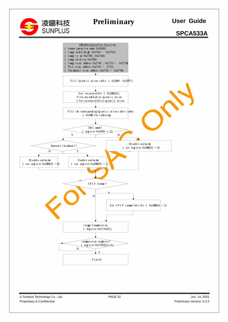
SPCA533A
© Sunplus Technology Co., Ltd.
Proprietary & Confidential
PAGE 52 Jun. 14, 2001
Preliminary Version: 0.2.0
Preliminary User Guide
Set JFIF compatible bit (0x2884[0] = 1)
trigger Compression(register 0x27A1[0])
JFIF format?
Fill Quantization table (0x2800 - 0x287F)
Set truncated bit (0x2885[0])0 for rounded after quantization1 for truncated after quantization
compression complete?(register 0x27B0[5]==1)
Finish
YN
YN
DRAM Controller Setting(camera operation mode 0x2000)(image width, height 0x2760 ~ 0x2763)(image type 0x270E, 0x2744)(image rotation 0x2786)(image start address 0x2749, 0x2753 ~ 0x2758)(VLC start address 0x2730 ~ 2732)(Thumbnail start address 0x2736 ~ 0x2738)
DSC mode?(register 0x2000 == 2)
Disable enthumb(set register 0x2883[0] = 0)
Generate thumbnail?
Disable enthumb(set register 0x2883[0] = 0)
Enable enthumb(set register 0x2883[0] = 1)
Y N
YN
Fill the corresponding Quantization table index(0x2880 for indexing)

SPCA533A
© Sunplus Technology Co., Ltd.
Proprietary & Confidential
PAGE 53 Jun. 14, 2001
Preliminary Version: 0.2.0
Preliminary User Guide
1.6.3 JPEG decompression
The first step of decompressing a JPEG file is parsing the header. The users must extract the quantization table from the header of the
JPEG file and fill them to the internal quantization table of the SPCA533. The image format (YUV422 or YUV420), restart code (if any)
information are derived from the header, too. These information must be determined and filled into the related registers before triggering
decompression. Again, The JPEG decompression engine works on the VLC data stream only, the header must be stripped by the firmware
in advance.
Even though the SPCA533A JPEG compression engine does not generated the restart codes, the decompression engine may decode a
file with restart codes. The restart code information resides in the header of the JFIF file which is lead by a marker of 0xFFDD. The users get
the information of how many MCU is inserted a restart code and write them into register 0x2888, 0x2889 to enable the restart code stripping
function. The JFIF compatible bit (register 0x2884[0]), while enabled, instruct the decompression engine to strip the 0X00 code after each
0Xff code in the VLC data stream.
The only way to check if the decompression is done without any error is checking the data size of the VLC data stream. If a file is
decompressed without any error, the total number of bits in the VLC data stream is the exact data size needed to recover the whole image.
The SPCA533A provides a flag JFIFend in register 0x2887[0] to check if there’re extra bits left in the VLC buffer after the decoding is done.
After the decompression is done, the JFIFend flag will be set if the EOI marker presents.
As the SPCA533A only embeds two quantization tables, the U/V components share the same table. This is enough for most applications.
If the users are going to decode a file with different quantazation table for U and V component, the decompression task could be paused
whenever each block (8x8 Y, U or V) is done. This allows the firmware to replace the quantization tables during decompression. However,
this will make the decompression time longer. It is not necessary in the normal case in which U and V components share the same
quantization table. Set StopEN bit ( register 0x2883[1]) to pause the JPEG engine while each block is done. Whenever each block is done,
the Blockend flag (register 0x2890[0]) will be set. After the quantization table is prepared, clear this flag to continue the decompress flow until
the end of next block.
The following flow chart are the control flow of JPEG decompression without stop and JPEG decompression in stop mode.

SPCA533A
© Sunplus Technology Co., Ltd.
Proprietary & Confidential
PAGE 54 Jun. 14, 2001
Preliminary Version: 0.2.0
Preliminary User Guide
Set JFIF compatible bit (0x2884[0] = 1)
trigger Decompression(register 0x27A1[1])
JFIF format?
Set the number of restart MCU number(0x2888, 0x2889)
Fill Quantization table (0x2800 - 0x287F)
Fill the corresponding Quantization table index(0x2880 for indexing)
Restart code embedded?(from JFIF header)
Set 0x2888, 0x2889 = 0 to disable MCUrestart code function (default)
decompression complete?(register 0x27B0[6]==1)
JFIF format?check JFIFend status(register 0x2887[0])
Finish Decompress CorrectDecompress Error
YN
YN
Y
N
YN
1 0
DRAM Controller Setting(camera operation mode 0x2000)(image width, height 0x2760 ~ 0x2763)(image type 0x270E, 0x2744)(image start address 0x2749, 0x2753 ~ 0x2758)(VLC start address 0x2730 ~ 2732)(VLC size 0x2720 ~ 0x2722)
If Y,U,V use different Q-table, the JPEG engine stops in the end of each block by setting the stopen bit (register 0x2883[1]). Here is the
flow chart.
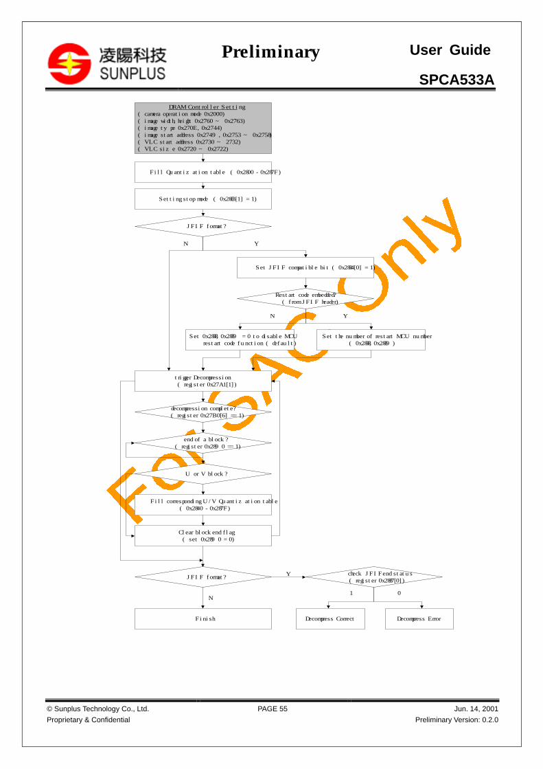
SPCA533A
© Sunplus Technology Co., Ltd.
Proprietary & Confidential
PAGE 55 Jun. 14, 2001
Preliminary Version: 0.2.0
Preliminary User Guide
Set JFIF compatible bit (0x2884[0] = 1)
trigger Decompression(register 0x27A1[1])
JFIF format?
Set the number of restart MCU number(0x2888, 0x2889)
Fill Quantization table (0x2800 - 0x287F)
Restart code embedded?(from JFIF header)
Set 0x2888, 0x2889 = 0 to disable MCUrestart code function (default)
decompression complete?(register 0x27B0[6] == 1)
JFIF format?check JFIFend status(register 0x2887[0])
Finish Decompress CorrectDecompress Error
YN
YN
Y
N1 0
Setting stop mode (0x2883[1] = 1)
end of a block?(register 0x2890 == 1)
U or V block?
Fill corresponding U/V Quantization table(0x2840 - 0x287F)
Clear blockend flag(set 0x2890 = 0)
DRAM Controller Setting(camera operation mode 0x2000)(image width, height 0x2760 ~ 0x2763)(image type 0x270E, 0x2744)(image start address 0x2749, 0x2753 ~ 0x2758)(VLC start address 0x2730 ~ 2732)(VLC size 0x2720 ~ 0x2722)

SPCA533A
© Sunplus Technology Co., Ltd.
Proprietary & Confidential
PAGE 56 Jun. 14, 2001
Preliminary Version: 0.2.0
Preliminary User Guide
1.7 USB bus interface
The SPCA533A implements ten USB endpoints. The main features of the endpoints are described in the following table.
Interface Endpoint Type Function
NA 0 Control Handles standard and vendor command data
0 1 Iso-in Transmits video image to the host
1 2 Bulk-in Transmits data to the host
1 3 Bulk-out Receives data from the host
1 4 Interrupt-in Transmits event data to the host
2 5 Interrupt-in Transmits audio events to the host
3 6 Iso-in Transmit audio data to the host
4 7 Bulk-in Transmits data to the host
4 8 Bulk-out Receives data from the host
4 9 Interrupt-in Transmits event data to the host
1.7.1 USB Vendor CommandIn the SPCA533, all standard commands but Get-Descriptor are processed by hardware state machine. For Get-Descriptor and the
vendor command, the embedded USB controller latches the 8-byte data in the SETUP packet and then interrupts the CPU. After being
interrupted, the CPU reads the 8-byte data, interprets it, and executes the command or prepares the appropriate data if necessary.
USB Vendor Command for Register Read/Write (example)
Command BmReqType BRequest WValue WIndex Wlength
Read 0Xc0 0X00 Reserved address 1
Write 0X40 0X00 High byte: reserved
Low byte: write value
address 0
USB Vendor Command for Image Upload (example)
Command BmReqType Brequest WValue Windex Wlength
get thumbnail 0X40 0X01 Image index 0X0000 0X0000
get image 0X40 0X01 Image index 0X0001 0X0000
get FAT 0X40 0X01 Reserved 0X0002 0X0000
get status 0Xc0 0X01 Reserved 0X0003 0X0001
The vendor commands may presents Data-in, Data-out or just the response phase. The flowing diagram shows the control flow for all type of
transfers for Vendor Commands:
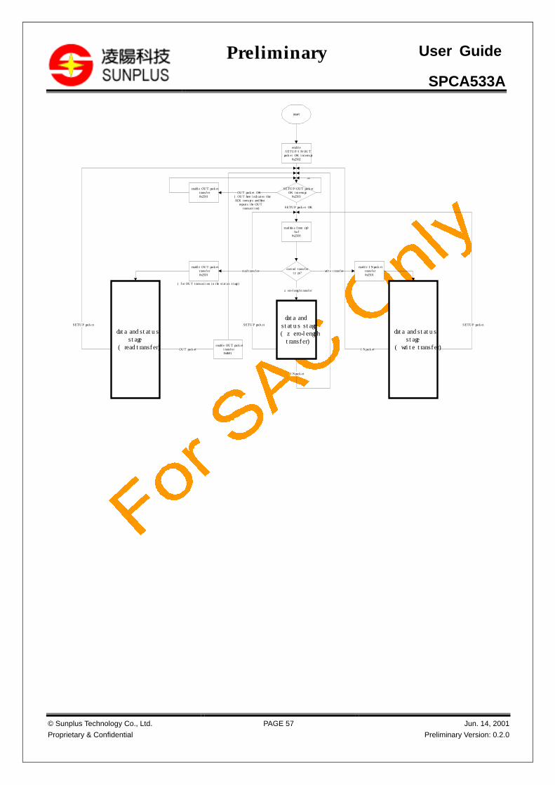
SPCA533A
© Sunplus Technology Co., Ltd.
Proprietary & Confidential
PAGE 57 Jun. 14, 2001
Preliminary Version: 0.2.0
Preliminary User Guide
read data from ep0 buf0x2500
enable SETUP/IN/OUT packet OK interrupt
0x2502
SETUP/OUT packet OK interrupt0x2503
control transfer type?
zero-length transfer
IN packet
SETUP packetSETUP packet SETUP packet
IN packetOUT packet
enable OUT packet transfer0x2501
SETUP packet OK
no
enable IN packet transfer0x2501
write transferread transfer
enable OUT packet transfer0x8501
enable OUT packet transfer0x2501
OUT packet OK
start
data and status stage
(read transfer)
data and status stage (zero-length transfer)
data and status stage
(write transfer)
(for OUT transaction in the status stage)
(OUT here indicates that ACK corrupts and Host repeats the OUT transaction)

SPCA533A
© Sunplus Technology Co., Ltd.
Proprietary & Confidential
PAGE 58 Jun. 14, 2001
Preliminary Version: 0.2.0
Preliminary User Guide
data and status stage (read transfer)
write IN data to ep0 buf0x2500
enable IN packet transfer0x2501
read IN/OUT/SETOK register0x2503
IN PC
(DATA) device
ACK PC
set INOK = 1
set interrupt
set INEN = 0
IN/OUT/SETOK?
IN packet OK
OUT packet OK(Read transfer completed)
SETUP packet OK
hardware
Note: The diagram in the "hardware" block is only an example.The out data transaction may also be presented in the diagram for the status stage
IN Data complete?
yes
Set ep0INstl
Disable ep0INstl

SPCA533A
© Sunplus Technology Co., Ltd.
Proprietary & Confidential
PAGE 59 Jun. 14, 2001
Preliminary Version: 0.2.0
Preliminary User Guide
data and status stage (write transfer)
enable OUT packet transfer0x2501
read IN/OUT/SETOK register0x2503
OUT PC
(DATA)
deviceACK
PC
set OUTOK = 1
set interrupt
set OUTEN = 0
IN/OUT/SETOK?
OUT packet OK
SETUP packet OKIN packet OK
hardware
read OUT data0x2500
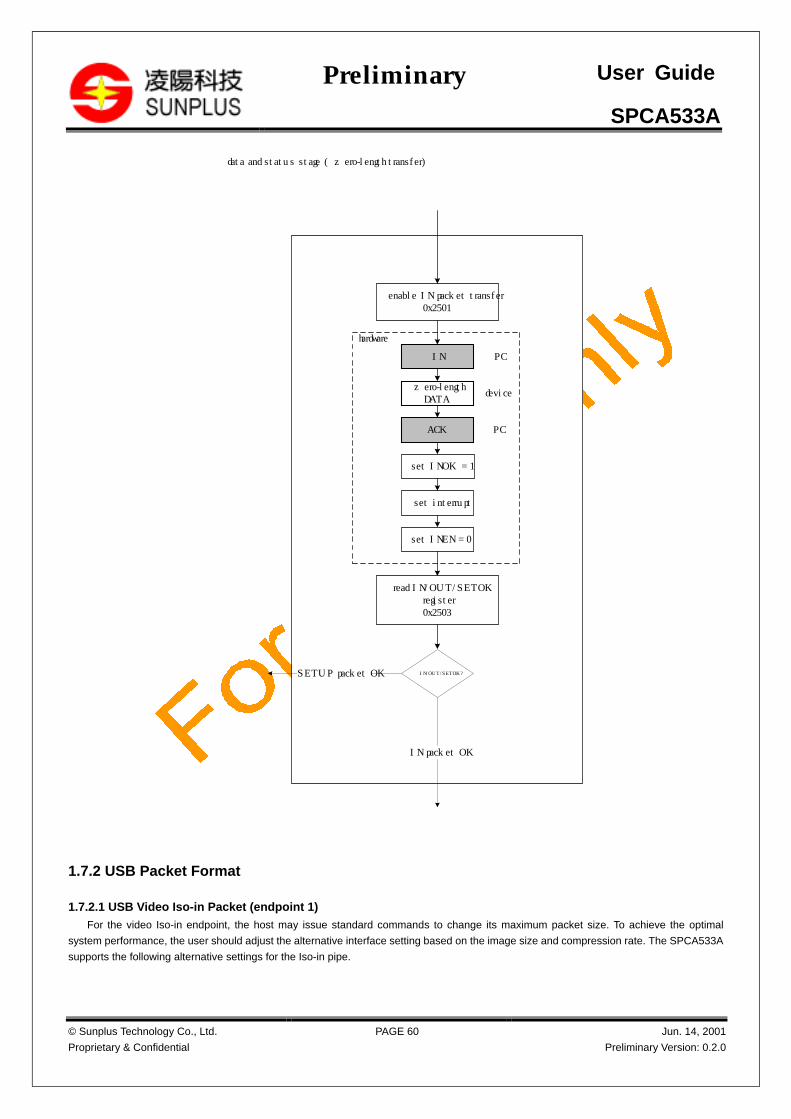
SPCA533A
© Sunplus Technology Co., Ltd.
Proprietary & Confidential
PAGE 60 Jun. 14, 2001
Preliminary Version: 0.2.0
Preliminary User Guide
data and status stage (zero-length transfer)
enable IN packet transfer0x2501
read IN/OUT/SETOK register0x2503
IN PC
zero-length DATA
device
ACK PC
set INOK = 1
set interrupt
set INEN = 0
IN/OUT/SETOK?
IN packet OK
SETUP packet OK
hardware
1.7.2 USB Packet Format
1.7.2.1 USB Video Iso-in Packet (endpoint 1)
For the video Iso-in endpoint, the host may issue standard commands to change its maximum packet size. To achieve the optimal
system performance, the user should adjust the alternative interface setting based on the image size and compression rate. The SPCA533A
supports the following alternative settings for the Iso-in pipe.

SPCA533A
© Sunplus Technology Co., Ltd.
Proprietary & Confidential
PAGE 61 Jun. 14, 2001
Preliminary Version: 0.2.0
Preliminary User Guide
Alternative Interface Setting Maximum Packet Size (bytes)
0 0
1 128
2 384
3 512
4 640
5 768
6 896
7 1023
The SPCA533A transmits the video isochronous packets with the full-size (maximum packet size) when the VidFulPktEn register is set
to 1. When there is not sufficient data to construct a full-size packet, the SPCA533A sends a zero-length data packet. The video Iso packets
are divided into two types: SOF (start of frame) packet and normal image packet. When VidFulPktEn register is cleared, short packets are
sent and no stuffing zero is applied to the end of the packets.
1.7.2.2 USB BULK-IN Packet (endpoint 2, 7)
The maximum packet size is fixed at 64 bytes. Short packets transmission and STALL response for the pipe are supported.
1.7.2.3 USB BULK-OUT Packet (endpoint 3, 8)
The maximum packet size is fixed at 64 bytes. Short packets transmission and STALL response for the pipe are supported.
1.7.2.4 USB Interrupt-IN Packet (endpoint 4, 9)
The maximum packet size is fixed at 64 bytes. Short packets transmission and STALL response for the pipe are supported.
1.7.2.5 Audio INTERRUPT-IN pipe (endpoint 5)
The maximum packet size is fixed at two bytes. The CPU should program the AudIntDataL/AudIntDataH registers (register 0x2504 and
0x2505) after it detects a new event. The USB controller sends the interrupt data to the host only after AudIntDataH register 0x2505 is
written.
1.7.2.6 Audio ISO-IN Pipe (endpoint 6)
For the audio Iso-in pipe, the host may issue standard commands to change its maximum packet size. The following table shows the
maximum packet sizes for the available alternative interface settings.
Alternative Interface Setting Maximum Packet Size (bytes)
0 0
1 16
2 32
3 48
4 64
5 80
6 96
7 112
8 128
9 144
10 160
11 176
12 192
13 208
14 256
15 512

SPCA533A
© Sunplus Technology Co., Ltd.
Proprietary & Confidential
PAGE 62 Jun. 14, 2001
Preliminary Version: 0.2.0
Preliminary User Guide
1.7.3 Bulk-Only Protocol Support
The SPCA533A supports Bulk-Only protocol used in MSDC and SIDC. In the command phase, Bulk-out pipe should be enabled. The
CPU reads the data in the Bulk-out buffer and decodes the command. The sequence is shown as follows:
Start
Set BulkOutEn
BulkOutAckedInterrupt
ReadBulkOutBufCnt
ReadBulkOutData
Last bytein Packet?
Last byte for the command block
ValidCommand?
ResponsePhase
DataInPhase
DataOutPhase
ResponsePhase
ResponsePhase
yes
no
no
yes
Set BulkInStl, BulkOutStl
yes
no
Command Phase
If the command is an unknown command, the Bulk-out and Bulk-in pipes can be stalled by setting the BulkInStl/BulkOutStl registers. If
the command is otherwise an OUT command, the host sends data to the SPCA533A and there exists a data out phase. In the data out
phase, the CPU reads data in the Bulk-out buffer. The Bulk-out buffer data can also be moved to some other buffers by the DMA mechanism.
Note that the DMA source (DMAUUSBSrc register 0x2510) should be specified when the DMA function is applied.

SPCA533A
© Sunplus Technology Co., Ltd.
Proprietary & Confidential
PAGE 63 Jun. 14, 2001
Preliminary Version: 0.2.0
Preliminary User Guide
Set BulkOutEn
BulkOutAckedInterrupt
ReadBulkOutBufCnt
ReadBulkOutData
Last bytein Packet?
Last byte for the data block?
Error/UserCancel?
ResponsePhase
yes
no
no
yes
Set BulkInStl, BulkOutStl
no
yes
DataOut Phase
If the command is instead an in command, the CPU should writes data in the Bulk-in buffer and enable the Bulk-in pipe. The
BulkInAcked interrupt indicates the data has been successfully transmitted to the host. As well as for the Bulk-out pipe, the DMA mechanism
can be applied here to move data to the Bulk-in buffer. Still note that DMAUSBDst should be specified.
DataIn Phase
WriteBulkInData
BulkInAckedInterrupt
Last byte?
SetBulkInEn
ResponsePhase
In the response phase, the CPU writes the response data to the Bulk-in buffer and enable the Bulk-in pipe. The BulkInAcked interrupt
indicates the host has successfully received the response and sent an ACK packet to SPCA533. For unknown commands, a response
phase would be presented after the standard Clear-Feature command and thus the stall condition can be cleared in the response phase.
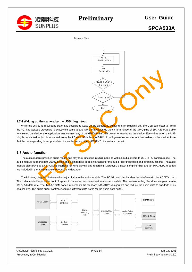
SPCA533A
© Sunplus Technology Co., Ltd.
Proprietary & Confidential
PAGE 64 Jun. 14, 2001
Preliminary Version: 0.2.0
Preliminary User Guide
Response Phase
WriteBulkInData
BulkInAckedInterrupt
Last byte?
SetBulkInEn
End
1.7.4 Waking up the camera by the USB plug in/out
While the device is in suspend state, it is possible to wake up the camera by pulgging-in (or plugging-out) the USB connector to (from)
the PC. The wakeup procedure is exactly the same as any GPIO that wakes up the camera. Since all the GPIO pins of SPCA533A are able
to wake up the device, the application may connect any of the GPIO to the USB power for waking up the device. Every time when the USB
plug is connected to (or disconnected from) the PC (or USB hub), the GPIO pin will generates an interrupt that wakes up the device. Note
that the corresponding interrupt enable bit must be set and the UIRSMINT bit must also be set.
1.8 Audio function
The audio module provides audio record and playback functions in DSC mode as well as audio stream to USB in PC-camera mode. The
audio module supports both AC‘97 codec and a embedded codec interfaces for the audio record/playback and stream functions. The audio
module also provides an SPCA751 interface for MP3 playing and recording. Moreover, a down-sampling filter and an IMA-ADPCM codec
are included in the audio module to reduce the data rate.
The following diagram illustrates the major blocks in the audio module. The AC ‘97 controller handles the interface with the AC ’97 codec.
The codec controller provides control signals to the codec and receives/transmits audio data. The down-sampling filter downsamples data to
1/2 or 1/6 data rate. The IMA-ADPCM codec implements the standard IMA-ADPCM algorithm and reduce the audio data to one-forth of its
original size. The audio buffer controller controls different data paths for the audio data buffer.
AC'97Controller
AC'97 Codec
Audio BufferController
SRAM 1KX8
EmbeddedCodec
CodecController
Down-sampling
Filter
IMA-ADPCMCodec
USBController
CPU & Global

SPCA533A
© Sunplus Technology Co., Ltd.
Proprietary & Confidential
PAGE 65 Jun. 14, 2001
Preliminary Version: 0.2.0
Preliminary User Guide
1.8.1 AC ‘97 Controller
The AC‘97 controller is fully compatible with the AC‘97 specification. It provides a digital interface (AC-link) to access an AC‘97 codec.
The AC-link is a bi-directional, fixed rate, serial PCM digital stream. It handles multiple input and output audio streams, as well as control
register accesses. The audio stream format can be programmed to be as stereo or mono with 8-bit or 16-bit PCM precision.
The diagram shown below depicts the control flow to access registers of the AC ‘97 codec. DO select the correct multiplexed pins by setting
the corresponding global registers before any further action. The write command provides write function to the AC’97 registers while the read
command provides the read counterpart. For write commands, set AC97En to 1 to enable the AC ‘97 controller. Write the desired AC ’97
register address and data in the AuOutAddr and AuWData(L and H) registers respectively. Write 1 to the AuOutReg, then, to trigger the
outgoing process in the next AC-link frame. AuOutBusy is then polled to check whether the data has been written to the AC‘97 codec.
In the AC-link interface, the command can be either write or read, as determined by the MSB of the register address specified. Thus write the
desired AC ‘97 register address to the AuOutAddr with 1 for the MSB when reading the register value from the AC ’97 codec. Write 1 to the
AuOutReg as in the write command. Check the AuInVld, then, to see if the register data has been stored in the AuInData(L and H) register.
Remember to clear AuInVld to 0 after you read the AuInData. Any further register data from the AC ‘97 would be blocked if the AuInVld
remains 1.
AC'97 RegisterWrite Command
Set AC'97En to 1
Write AuOutAddr
Write AuWDataL,AuWDataH
Set AuOurReg to 1
Done
AuOutBusy?yes
no
Read AuInDataL,AuInDataH
AC'97 RegisterRead Command
Set AC'97En to 1
Write AuOutAddr
Set AuOurReg to 1
AuInVld?no
yes
Done
Clear AuInVld to 0
1.8.2 Codec Controller
The Codec controller collects the 8-bit audio data from/to the embedded codec. The sampling rate/ playback rate for the codec can be
8KHz, 24KHz, 44.1KHz and 48KHz. To enable the ADC, write 0 to ADCceb and 1 to ADCshe, ADCagce and ADCade.

SPCA533A
© Sunplus Technology Co., Ltd.
Proprietary & Confidential
PAGE 66 Jun. 14, 2001
Preliminary Version: 0.2.0
Preliminary User Guide
1.8.3 Down-sampling Filter
The down-sampling filter provides two down-sample modes: 2-times and 6-times. Low pass filters are used to avoid aliasing errors. The
low-pass filter gain is 15/16, (15/16)2 for 2-times and 6-times down-sampling respectively.
1.8.4 ADPCM Codec
The ADPCM Codec implements the standard IMA-ADPCM algorithm. The encoder encodes a stream of data into a series of pages (or
packets). Each page contains a 4-byte header with state information and a series of 4-bit compressed samples (as depicted in the following
table). Each 4-bit value encodes the differences between two successive 16-bit uncompressed audio data. The decoder decodes pages of
compressed data into a series of 16-bit PCM audio data.
Two page modes are supported. For 512-byte page mode, one single page accounts for 1017 data samples (one sample in the header and
1016 samples in the remaining 508 bytes of compressed data) while 505 samples for 256-byte mode.
Header Bytes Compressed Data Bytes
byte0 byte1 byte2 byte3 byte4 byte5 … byte510 byte511
sample0
(low byte)
sample0
(high byte)
index 0 encoded
data
for sample
1 & 2
encoded
data
for sample
3 & 4
encoded
data
for sample
1014 &
1015
encoded
data
for sample
1016 &
1017
Note. the table illustrates a page in the 512-byte page mode
1.8.5 Audio Buffer Controller
The audio buffer controller handles seven different data paths for the audio buffer: AC‘97/CODEC-to-CPU(record), AC’97/CODEC-to-
USB(stream) and CPU-to-AC‘97/CODEC(playback), AC‘97/CODEC-to-DMA(record), AC‘97/CODEC-to-DRAM(record), DRAM-to-
AC‘97/CODEC(playback) and DMA-to-AC‘97/CODEC(playback). or the record function, the audio data is written to the audio buffer by the
AC‘97/CODEC controller and then read out by CPU/DRAM/DMAC. The corresponding control flow is shown below. If an AC’97 codec is
used, set AuBMode(audio buffer mode) to 1, 3 or 5 first to select the AC‘97/CODEC-to-CPU/DRAM/DMA data path. Set AuStereo, Au16bit
and PCM8En to the desired value. Set AuDSMode(down-sampling mode) to the desired down-sampling ratio. Set AuBLThr(audio buffer low
thershold) for a low threshold interrupt. This helps CPU control the amount of data in the audio buffer. If ADCPCM codec is used, set
ADPCMPageMode to 256bytes/page or 512bytes/page. The last but not the least, set AC’97En and ADPCMEncEn(ADPCM encoder enable)
to enable the whole function. CPU is now responsible for reading the data in the audio buffer. It can keep reading the buffer until the
AuBUnLThr(under low threshold) interrupt is invoked.
The control flow of the ADC record function is basically the same as the AC‘97 record. Yet, the embedded ADC needs a few more steps
when starting to function. DO set ADCceb to 0 and ADCshe – ADCade to 1 to configure the ADC. Unmute the ADC by setting ADCMute to 0.
Note that if ADPCM codec is used, set the Au16bit to 1 since the ADCPCM codec converts only the 16bit data.
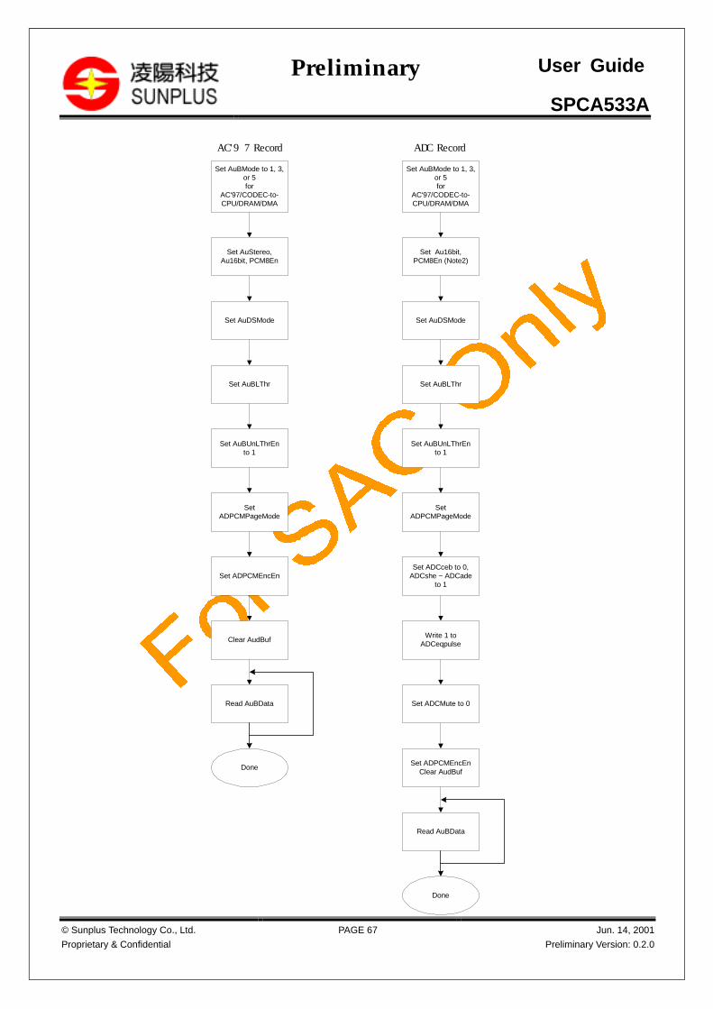
SPCA533A
© Sunplus Technology Co., Ltd.
Proprietary & Confidential
PAGE 67 Jun. 14, 2001
Preliminary Version: 0.2.0
Preliminary User Guide
Set AuBMode to 1, 3,or 5for
AC'97/CODEC-to-CPU/DRAM/DMA
Done
ADC Record
Set Au16bit,PCM8En (Note2)
Set AuDSMode
Set AuBLThr
Set AuBUnLThrEnto 1
Set ADPCMEncEnClear AudBuf
Read AuBData
SetADPCMPageMode
Set ADCceb to 0,ADCshe ~ ADCade
to 1
Set AuBMode to 1, 3,or 5for
AC'97/CODEC-to-CPU/DRAM/DMA
Done
AC'97 Record
Set AuStereo,Au16bit, PCM8En
Set AuDSMode
Set AuBLThr
Set AuBUnLThrEnto 1
Clear AudBuf
Read AuBData
SetADPCMPageMode
Set ADPCMEncEn
Write 1 toADCeqpulse
Set ADCMute to 0

SPCA533A
© Sunplus Technology Co., Ltd.
Proprietary & Confidential
PAGE 68 Jun. 14, 2001
Preliminary Version: 0.2.0
Preliminary User Guide
The diagram below illustrates the control flow of AC‘97 and ADC stream (data path AC’97/CODEC-to-USB) function. The major steps
are identical with that of the record function except that the USB controller here reads the audio buffer automatically.
Set AuBMode to 0for
AC'97/CODEC-to-USB
Done
AC'97 Stream
Set AuStereo,Au16bit, PCM8En
Set AuDSMode
Set AC'97En to 1
Set AuBMode to 0for
AC'97/CODEC-to-USB
ADC Stream
Set AuStereo to 0,Au16bit to 0,
PCM8En to desiredvalue
Set AuDSMode
Done
Set ADCceb to 0,ADCshe ~ ADCade
to 1
Write 1 toADCeqpulse
Set ADCMute to 0
To enable the playback function, set AuBMode to 2, 4 or 6 for data path CPU/DRAM/DMA-to-AC‘97. Set AuStereo, Au16bit and
PCM8En to the desired value. Set AuDFreq to select the playback frequency. Set AuBHThr (audio buffer high threshold) and AuBOvHThrEn
(over high threshold enable) to enable the interrupt function when the amount of data in the audio buffer is over the high threshold. If ADPCM
decoder is used, set the ADPCMPageMode and ADPCMDecEn (ADPCM decoder enable). Set AC’97En at last to enable the function. The
CPU/DRAM/DMA is now responsible for writing data (uncompressed or compressed) to the audio buffer. It can keep writing until the
AuBOvHThr interrup is detected.
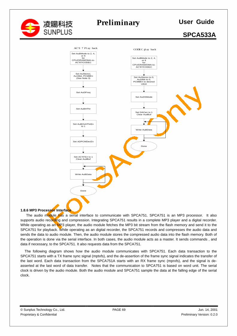
SPCA533A
© Sunplus Technology Co., Ltd.
Proprietary & Confidential
PAGE 69 Jun. 14, 2001
Preliminary Version: 0.2.0
Preliminary User Guide
Set AuBMode to 2, 4,or 6for
CPU/DRAM/DMA-to-AC'97/CODEC
AC'97 Playback
Set AuStereo,Au16bit, PCM8En
(See Note 3)
Set AuDFreq
Set AC'97En to 1Clear AudBuf
Set ADPCMDecEn
Done
Write AuBData
Set AuBHThr
Set AuBOvHThrEnto 1
Set AuBMode to 2, 4,or 6for
CPU/DRAM/DMA-to-AC'97/CODEC
CODEC playback
Set AuStereo to 0,Au16bit to 0,
PCM8En to desiredvalue
Set AuDSMode
Done
Set DACen to 1Clear AudBuf
Write AuBData
1.8.6 MP3 Processor Interface
The audio module has a serial interface to communicate with SPCA751. SPCA751 is an MP3 processor. It alsosupports audio recording and compression. Integrating SPCA751 results in a complete MP3 player and a digital recorder.While operating as an MP3 player, the audio module fetches the MP3 bit stream from the flash memory and send it to theSPCA751 for playback. While operating as an digital recorder, the SPCA751 records and compresses the audio data andsends the data to audio module. Then, the audio module stores the compressed audio data into the flash memory. Both ofthe operation is done via the serial interface. In both cases, the audio module acts as a master. It sends commands , anddata if necessary, to the SPCA751. It also requests data from the SPCA751.
The following diagram shows how the audio module communicates with SPCA751. Each data transaction to theSPCA751 starts with a TX frame sync signal (mptxfs), and the de-assertion of the frame sync signal indicates the transfer ofthe last word. Each data transaction from the SPCA751A starts with an RX frame sync (mprxfs), and the signal is de-asserted at the last word of data transfer. Notes that the communication to SPCA751 is based on word unit. The serialclock is driven by the audio module. Both the audio module and SPCA751 sample the data at the falling edge of the serialclock.

SPCA533A
© Sunplus Technology Co., Ltd.
Proprietary & Confidential
PAGE 70 Jun. 14, 2001
Preliminary Version: 0.2.0
Preliminary User Guide
mpsiclk
mpfs
mpd B15 B14 B13 B12 B11 B10 B9 B8 B7 B6 B5 B4 B3 B2 B1 B0
16 bits command waveform
512 bytes data wavefrom
falling edge latch
B15
B14
B13
B12
B11
B10
B9
B8
B7
B6
B5
B6
B5
B4
B3
B2
B1
B0
B15
B14
B13
B12
B11
B10
B9
B8
B7
B6
B5
B6
B5
B4
B3
B2
B1
B0
last byte
Camera ASICSPCA751
(MP3)
mpfs
mpsiclk
mpd
mpreset(gpio0)
mpfceb2
mpfceb1
mpsiclk
mpfs
mpd
1.8.7 Programming flow of the MP3 processor serial interface
mpsiwrnn=0
Communication with the MP3 processor
mpsilength=desiredvalue
mpsiprefetch=1
mpsiready
y
n
readdataport
last byte
finish
y
n
read
mpsiwrnn=1
mpsilength=desiredvalue
writedataport
mpsiready
y
n
last byte
finish
y
n
write
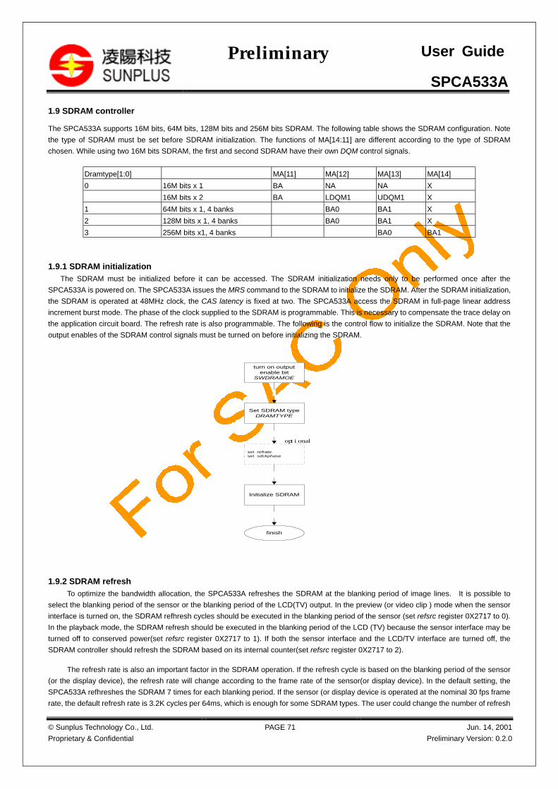
SPCA533A
© Sunplus Technology Co., Ltd.
Proprietary & Confidential
PAGE 71 Jun. 14, 2001
Preliminary Version: 0.2.0
Preliminary User Guide
1.9 SDRAM controller
The SPCA533A supports 16M bits, 64M bits, 128M bits and 256M bits SDRAM. The following table shows the SDRAM configuration. Note
the type of SDRAM must be set before SDRAM initialization. The functions of MA[14:11] are different according to the type of SDRAM
chosen. While using two 16M bits SDRAM, the first and second SDRAM have their own DQM control signals.
Dramtype[1:0] MA[11] MA[12] MA[13] MA[14]
0 16M bits x 1 BA NA NA X
16M bits x 2 BA LDQM1 UDQM1 X
1 64M bits x 1, 4 banks BA0 BA1 X
2 128M bits x 1, 4 banks BA0 BA1 X
3 256M bits x1, 4 banks BA0 BA1
1.9.1 SDRAM initialization
The SDRAM must be initialized before it can be accessed. The SDRAM initialization needs only to be performed once after the
SPCA533A is powered on. The SPCA533A issues the MRS command to the SDRAM to initialize the SDRAM. After the SDRAM initialization,
the SDRAM is operated at 48MHz clock, the CAS latency is fixed at two. The SPCA533A access the SDRAM in full-page linear address
increment burst mode. The phase of the clock supplied to the SDRAM is programmable. This is necessary to compensate the trace delay on
the application circuit board. The refresh rate is also programmable. The following is the control flow to initialize the SDRAM. Note that the
output enables of the SDRAM control signals must be turned on before initializing the SDRAM.
turn on outputenable bit
SWDRAMOE
Set SDRAM typeDRAMTYPE
set refrateset sdckphase
Initialize SDRAM
finish
optional
1.9.2 SDRAM refresh
To optimize the bandwidth allocation, the SPCA533A refreshes the SDRAM at the blanking period of image lines. It is possible to
select the blanking period of the sensor or the blanking period of the LCD(TV) output. In the preview (or video clip ) mode when the sensor
interface is turned on, the SDRAM refhresh cycles should be executed in the blanking period of the sensor (set refsrc register 0X2717 to 0).
In the playback mode, the SDRAM refresh should be executed in the blanking period of the LCD (TV) because the sensor interface may be
turned off to conserved power(set refsrc register 0X2717 to 1). If both the sensor interface and the LCD/TV interface are turned off, the
SDRAM controller should refresh the SDRAM based on its internal counter(set refsrc register 0X2717 to 2).
The refresh rate is also an important factor in the SDRAM operation. If the refresh cycle is based on the blanking period of the sensor
(or the display device), the refresh rate will change according to the frame rate of the sensor(or display device). In the default setting, the
SPCA533A refhreshes the SDRAM 7 times for each blanking period. If the sensor (or display device is operated at the nominal 30 fps frame
rate, the default refresh rate is 3.2K cycles per 64ms, which is enough for some SDRAM types. The user could change the number of refresh
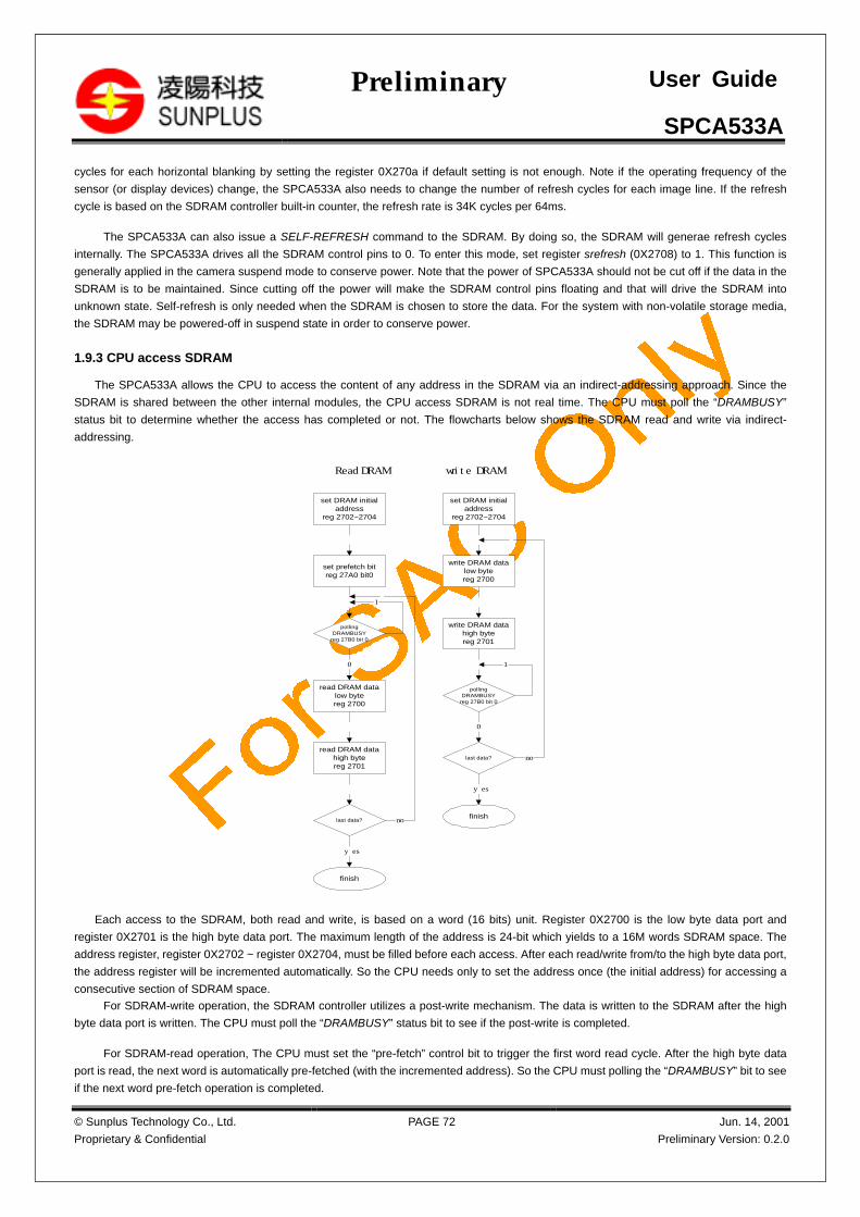
SPCA533A
© Sunplus Technology Co., Ltd.
Proprietary & Confidential
PAGE 72 Jun. 14, 2001
Preliminary Version: 0.2.0
Preliminary User Guide
cycles for each horizontal blanking by setting the register 0X270a if default setting is not enough. Note if the operating frequency of the
sensor (or display devices) change, the SPCA533A also needs to change the number of refresh cycles for each image line. If the refresh
cycle is based on the SDRAM controller built-in counter, the refresh rate is 34K cycles per 64ms.
The SPCA533A can also issue a SELF-REFRESH command to the SDRAM. By doing so, the SDRAM will generae refresh cycles
internally. The SPCA533A drives all the SDRAM control pins to 0. To enter this mode, set register srefresh (0X2708) to 1. This function is
generally applied in the camera suspend mode to conserve power. Note that the power of SPCA533A should not be cut off if the data in the
SDRAM is to be maintained. Since cutting off the power will make the SDRAM control pins floating and that will drive the SDRAM into
unknown state. Self-refresh is only needed when the SDRAM is chosen to store the data. For the system with non-volatile storage media,
the SDRAM may be powered-off in suspend state in order to conserve power.
1.9.3 CPU access SDRAM
The SPCA533A allows the CPU to access the content of any address in the SDRAM via an indirect-addressing approach. Since the
SDRAM is shared between the other internal modules, the CPU access SDRAM is not real time. The CPU must poll the “DRAMBUSY”
status bit to determine whether the access has completed or not. The flowcharts below shows the SDRAM read and write via indirect-
addressing.
Read DRAM
set DRAM initialaddress
reg 2702~2704
set prefetch bitreg 27A0 bit0
pollingDRAMBUSY
reg 27B0 bit 0
0
1
read DRAM datalow bytereg 2700
read DRAM datahigh bytereg 2701
last data?
no
yes
finish
set DRAM initialaddress
reg 2702~2704
pollingDRAMBUSY
reg 27B0 bit 0
0
1
write DRAM datalow bytereg 2700
write DRAM datahigh bytereg 2701
last data?
no
yes
finish
write DRAM
Each access to the SDRAM, both read and write, is based on a word (16 bits) unit. Register 0X2700 is the low byte data port and
register 0X2701 is the high byte data port. The maximum length of the address is 24-bit which yields to a 16M words SDRAM space. The
address register, register 0X2702 ~ register 0X2704, must be filled before each access. After each read/write from/to the high byte data port,
the address register will be incremented automatically. So the CPU needs only to set the address once (the initial address) for accessing a
consecutive section of SDRAM space.
For SDRAM-write operation, the SDRAM controller utilizes a post-write mechanism. The data is written to the SDRAM after the high
byte data port is written. The CPU must poll the “DRAMBUSY” status bit to see if the post-write is completed.
For SDRAM-read operation, The CPU must set the “pre-fetch” control bit to trigger the first word read cycle. After the high byte data
port is read, the next word is automatically pre-fetched (with the incremented address). So the CPU must polling the “DRAMBUSY” bit to see
if the next word pre-fetch operation is completed.

SPCA533A
© Sunplus Technology Co., Ltd.
Proprietary & Confidential
PAGE 73 Jun. 14, 2001
Preliminary Version: 0.2.0
Preliminary User Guide
1.9.4 Filling constant data to the SDRAM
The SPCA533A provides a fast operation to fill a constant value to the SDRAM. The address of the SDRAM to be filledmust be continuous. Only the initial address and the size of the SDRAM need to be specified. This hardware operation ismuch faster than filling the data by firmware word by word. The following is the flow control . In the diagram below, theCLRSIZE represent the size to be filled which is based on the number of words. Register 0X270B specifies the low bytes ofthe constant and register 0X270C specifies the high bytes of the constant.
Fill constant value to the SDRAM
Set initial addressreg 2702-2704
Set CLRSIZEregisters
2705-2706
trigger the clearaction
reg 27A0 bit1
pollingDRAMBUSY
reg 27b0 bit 0
0
1
finish
write CLRDATAregistes
270B-270C
1.9.5 Interface with DMA controller
The data sotred in the SDRAM can be moved to the other internal module of the SPCA533A by the DMA controller. The DMA control
flow is discussed in section 5.4. While most of the controls are done by the DMA controller, the SDRAM starting address must be specified
before starting the DMA operation. The starting address is programmed in registers (0X2750~0X2752).
1.9.6 Image data input control
The SDRAM is used as a temporary buffer during the camera operation. There are many options to control how the data is stored in the
SDRAM.
ImgType : The image type option chose between raw data, YUV422 data, YUV420 data, compressed data and non-compressed data.
Depending on the operation stage, this registers must be specified accordingly.
CapInt : The capture interval control. The control the input frame rate, especially in capturing the video data, the SPCA533A allows
the user to change the input frame rate. The SDRAM controller will drops the unwanted frames.
Size : The SDRAM controller requires the user to specify the image size in both the vertical and horizontal direction. The size is
specified based on the number of pixels, which must be multiples of 16. Since the JPEG engines work on 8x8 basic coding
units. The size of the image must complies to this criteria.
Fieldmode: The field mode register determines whether to re-ararnge the line sequence while writing the raw data in to the SDRAM
buffer. This is used in the interlaced CCD sensors. This option is only applied in the full frame raw data capture of an

SPCA533A
© Sunplus Technology Co., Ltd.
Proprietary & Confidential
PAGE 74 Jun. 14, 2001
Preliminary Version: 0.2.0
Preliminary User Guide
interlaced CCD sensor. In PC-camera or video clip mode, the users should always select one-field mode. The
SPCA533A also supports interlace-type CCD sensor operation, section 5.9.10 has more details.
1.9.7 Data format
The SDRAM controller is also responsible to generate the data formats for different applications. Three basic formats are
implemented in the SDRAM controller according to the data type selected. During uploading data to the PC via the USB bus or writing data
to the flash memory, the data are output according to the formats.
Raw data format : The raw data format is in the raster-scan sequence. If 10-bit raw data mode is selected, each pixel contains 2 bytes of
data. The first byte is low byte raw data, the second byte is high byte raw data. There are 6 zero-bit stuffed in the MSB of the high byte. If 8-
bit raw data mode is selected, each byte represents one pixel of raw data. The following diagram shows an example of a 16-pixel by 16-pixel
raw data. Each pixel (for both 8-bit raw data and 10-bit raw data) occupies a word of the SDRAM.
16 pixels
16 pixels
0 0 b9b8b7b6b5b4b3b2b1b00000
10-bit raw data
8-bit raw data0 0 b7b6b5b4b3b2b1b00000 0 0
high byte low byte
a pixel
YUV 422 format : The SPCA533A utilizes the standard JPEG compression algorithm. In the YUV422 format, the minimum coding unit (MCU)
is consisted of two Y-blocks, one U-block and one V-block. The size of each block is 8 pixels by 8 pixels. So the data sequence sent to the
JPEG engoine is YYUVYYUVYYU..,etc. Note that if the final data size is not multiples of the flash memory page size, The DMA controller will
stuff 0’s to the end of the page.
16 pixels
u3u2u1u0y7y6y5y4y3y2y1y0u4u5u6u7
low byte
v3v2v1v0y7y6y5y4y3y2y1y0v4v5v6v7
even pixels
odd pixel
high byte
16 pixels
Data is the SDRAM buffer
To JPEG engine
Y(8x8)
Y U V Y Y U V
YUV420 format : The YUV420 format is similar to YUV422 format, except that each MCU is consisted of four Y blocks, one U block and one
V block. The block sequence is YYYYUVYYYYUV…,etc. The following diagram shows an example of a 16-pixel by 16-pixl YUV420 image in
the SDRAM buffer. Note that in the odd lines, the UV data is not valid because in UV is subsampled in the vertical direction in the YUV420
format.
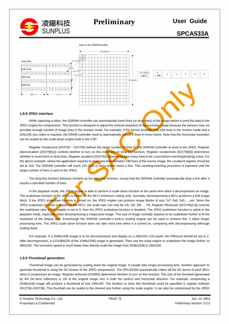
SPCA533A
© Sunplus Technology Co., Ltd.
Proprietary & Confidential
PAGE 75 Jun. 14, 2001
Preliminary Version: 0.2.0
Preliminary User Guide
16 pixels
u3u2u1u0y7y6y5y4y3y2y1y0u4u5u6u7
low byte
v3v2v1v0y7y6y5y4y3y2y1y0v4v5v6v7
even pixels
odd pixel
high byte
16 pixels
Data is the SDRAM buffer
To JPEG engine
Y(8x8)
Y Y Y U V
X X X X y7y6y5y4y3y2y1y0XXXX
X X X X y7y6y5y4y3y2y1y0XXXX
even line
odd line
even line
odd line
even pixels
even pixels
1.9.8 JPEG interface
While capturing a video, the SDRAM controller can automatically insert lines (or drop lines) of the image before it send the data to the
JPEG engine for compression. This function is designed to adjust the vertical resolution of the incoming image because the sensors may not
provides enough number of image lines in the monitor mode. For example, if the sensor provides only 238 lines in the monitor mode and a
320x240 size video is required, the DRAM controller need to automatically inserts 2 lines in every frame. Note that the horizontal resolution
can be scaled by the scale-down engine built in the CSP.
Register Vscalevsize (0X2792 ~ 0X2793) defines the target number of lines for the SDRAM controller to send to the JPEG. Register
dramvscaleen (0X2790[1]) controls whether to turn on this insert-line or drop-line function. Register vscalemode (0X2790[0]) determines
whether to insert liens or drop lines. Register vscalecnt (0X2791) determines how many lines to be count before inserting(droping) a line. For
the above example, where the application requires to insert two lines between 238 lines of the source image, the vscalecnt register shoud be
set to 118. The SDRAM controller will count 119 (118+1) lines before insert a line. This counting-inserting procedure is repeated until the
target number of lines is sent to the JPEG.
The drop-line function behaves similarly as the inset-line function, except that the SDRAM controller automatically drop a line after it
counts a specified number of lines.
In the playback mode, the JPEG engine is able to perform a scale down function at the same time when it decompresses an image.
The scaledown function of the JPEG is based on the MCU (minimum coding unit). Normally, decompressing a MCU produces a 8x8 image
block. If the JPEG scaledown function is turned on, the JPEG engine can produce image blocks of size 7x7, 6x6, 5x5,….,etc. Since the
JPEG scaledown function is based on the MCU, the scale ratio can only be 1/8, 2/8, 3/8, …7/8. Register Pbrescale (0X2745[2:0]) controls
the scaledown ratio. If this register is set to 0, then the JPEG scaledown function is disabled. The JPEG scaledown function is usfule in the
playback mode, especially when decompressing a mega-pixel image. This size of image normally requires to be scaledown further to fit the
resolution of the display size. Eventhough the SDRAM controller’s built-in scaling engine can be used to achieve this, it takes longer
processing time. The JPEG scale down function does not take extra time when it is turned on, comparing with decompressing withough
scaling down.
For example, if a 2048x1536 image is to be decompressed and display on a 280x220 LCD panel, the PBrescal should be set to 2.
After decompression, a 512x384(2/8 of the 1048x1536) image is generated. Then use the sclae engine to scaledown the image further, to
280x220. The execution speed is much faster than directly scale the image from 2048x1536 to 280x220.
1.9.9 Thumbnail generation
Thumbnail image can be generated by scaling down the original image. It usually take longer processing time. Another approach to
generate thumbnail is using the DC-terams of the JPEG compression. The SPCA533A automatically collect all the DC-terms of each MCU
when it compresses an image. Register enthumb (0X2883) determines whether to turn on this function. The size of the thumbail (generated
by the DC-term collection) is 1/8 of the original image size in both the verticvl and horizontal direction. For example, compresing a
2048x1536 image will produce a thumbnail of size 256x192. The location to store this thumbnail could be specified in register tmbstart
(0X2736~0X2738). This thumbail can be scaled to the desired size further using the scale engine. It can also be compressed by the JPEG

SPCA533A
© Sunplus Technology Co., Ltd.
Proprietary & Confidential
PAGE 76 Jun. 14, 2001
Preliminary Version: 0.2.0
Preliminary User Guide
engine.
1.9.10 Image-Processing engine
The image-processing engine embedded in the SDRAM controller performs a wide range of tasks to assist the firmware during the
camera operation. Many specialized camera features can be achieved by the image-processing engine. The image-process engine also
boosts the overall performance of the SPCA533. The image-process engine provides the following functions.
(a) Image-scaling operation
(b) Image-rotation operation
(c) Copy & paste operation
(d) Date-stamping operation
(e) DRAM-to-DRAM DMA operation
(f) bad-pixel correction
(g) inter-frame raw data subtraction
(h) YUV420-to-YUV422 conversion
Among the functions supported by the image-process engine, many of them operate on two image buffers. For example, the scaling
function scales the image in the source image buffer and stores the result into another image buffer. There are also functions which operated
on a single image buffer. For example, the bad pixel correction function. The SPCA533A defines two indices to indicate the starting address
(in the SDRAM) of the source image buffer (usually image buffer A) and the target image buffer (image buffer B). The offsets of the image
buffer are also defined. The offsets are useful in functions like the copy & past function, in which the copy location of the source image buffer
and paste location of the target image buffer must be specified. Also the sizes of the image buffer are also defined. The size parameters are
useful for the image-processing engine to calculate the SDRAM address.
The general operation flow of the image-process engine is
1) Select the function in register 0x2770[7:4]
2) Programming the starting addresses, buffer size, offsets of both source and target (if any) image buffer.
3) Trigger the operation by writing 1 to 0x27A1[7]
4) Polling the register 0x27B0[7] to check if the operation is done.
1.9.10.1 Image-scaling operation
The scaling function provides both image scaling-up and scaling-down operations in the YUV422 domain. The engine performs one-
dimension scaling. To scale up/down an image, the engine must be triggered twice. One for the horizontal scaling, the other for the vertical
scaling. Appropriated filters are applied in the scaling function to achieve good image quality. The scaling function is usually executed after
the image is captured and converted to the YUV format by the CDSP. It can be used to generate an image of the resolution the application
intends or generate a 160x120 thumbnail image. The scaling function also enables the SPCA533A to do digital zoom. In the playback
modes, the scaling function enables the SPCA533A to generate an image of size exactly fitting the resolution of the display devices.
While performing the scaling function, the Image buffer A always points to the source image and image buffer B always points to the
target image. Both the image width and height must be a multiple of 4. The scaling factor is defined in register 0X277F and 0X2780, which is
a 16 bit fractional number. For image scaling down, the scale factor represents the target-to-source image size ratio. For image scaling up,
the scaling factor represents the source-to-target image size ratio. Accessing the image buffer in the vertical direction takes longer time than
accessing the buffer in the horizontal direction. In the application, the firmware must reduce the data access to the image buffer in the
vertical direction to speedup the scaling. The following rules must be followed.
1) Scaling-down: horizontal scaling first, then vertical scaling
2) Scaling-up: vertical scaling first, then horizontal scaling

SPCA533A
© Sunplus Technology Co., Ltd.
Proprietary & Confidential
PAGE 77 Jun. 14, 2001
Preliminary Version: 0.2.0
Preliminary User Guide
Example of image scaling-down :
The source image size is 1600x1200, locates in the SDRAM starting from address 0x000000 to 0x1D4BFF.
The target image size is 280x220, locates in the SDRAM starting from address 0x000000 to 0x00F099.
The scaling factors:
Horizontal: 280/1600 = 0.175 => represented as 16-bit fraction = 11468.8 (0.175x65536)
=> round up = 11469
=> represented as hexadecimal digits = 0x2CCD
Vertical: 220/1200 = 0.183… => represented as 16-bit fraction = 12014.9 (0.183… x65536)
=> round up = 12015
=> represented as hexadecimal digits = 0x2EEF
done ?(0x27B0[7]?=1)
yes
set image buffer Astarting addrsss =
0x000000width = 1600height = 1200
(0x2771[7:0]=0x00,0x2772[7:0]=0x00,0x2773[7:0]=0x00,0x2777[7:0]=0x40,0x2778[3:0]=0x06,0x2779[7:0]=0xb0,0x277A[3:0]=0x04)
select operationmode
set scaling mode(horizontal, filter,
scaling-down)(0x2770[2:0]=0x12)
no
start imageprocessing
(0x27A1[7]=1)
set image buffer Bstarting addrsss =
0x200000width = 280
height = 1200(0x2774[7:0]=0x00,0x2775[7:0]=0x00,0x2776[7:0]=0x20,0x277B[7:0]=0x18,0x277C[3:0]=0x01,0x277D[7:0]=0xb0,0x277E[3:0]=0x04)
set image buffer Astarting addrsss =
0x200000width = 280
height = 1200(0x2774[7:0]=0x00,0x2775[7:0]=0x00,0x2776[7:0]=0x20,0x277B[7:0]=0x18,0x277C[3:0]=0x01,0x277D[7:0]=0xb0,0x277E[3:0]=0x04)
set image buffer Bstarting addrsss =
0x000000width = 280height = 220
(0x2774[7:0]=0x00,0x2775[7:0]=0x00,0x2776[7:0]=0x00,0x277B[7:0]=0x18,0x277C[3:0]=0x01,0x277D[7:0]=0xdc,0x277E[3:0]=0x00)
done ?(0x27B0[7]?=1)
yes
select opertion modeset scaling mode
(vertical, filter,scaling-down)
(0x2770[2:0]=0x13)
no
start imageprocessing
(0x27A1[7]=1)
set scaling factor(0x2780[7:0]=0x2c0x277F[7:0]=0xcd)
set scaling factor(0x2780[7:0]=0x2e0x277F[7:0]=0xef)
scaling-down isfinished
scaling-down flow chart

SPCA533A
© Sunplus Technology Co., Ltd.
Proprietary & Confidential
PAGE 78 Jun. 14, 2001
Preliminary Version: 0.2.0
Preliminary User Guide
Example of the image scaling-up
The source image size is 160x120, locates in the SDRAM staring from address 0x000000 to 0x004AFF.
The target image size is 280x220, locates in the SDRAM starting from address 0x000000 to 0x00F099.
The scaling factors:
Horizontal: 160/280 = 0.571… => represented as 16-bit fraction = 37449.1 (0.571…x65536)
=> round down = 37449
=> represented as hexadecimal digits = 0x9249
Vertical: 120/220 = 0.545… => represented as 16-bit fraction = 35746.9 (0.545…x65536)
=> round down = 35746
=> represented as hexadecimal digits = 0x8BA2
scaling-up flow chart
done ?(0x27B0[7]?=1)
yes
set image buffer Astarting addrsss =
0x000000width = 160height = 120
(0x2771[7:0]=0x00,0x2772[7:0]=0x00,0x2773[7:0]=0x00,0x2777[7:0]=0xa0,0x2778[3:0]=0x00,0x2779[7:0]=0x78,0x277A[3:0]=0x00)
select operationmode
set scaling mode(vertical, filter,
scaling-up)(0x2770[7:0]=0x17)
start imageprocessing
(0x27A1[7]=1)
set image buffer Bstarting addrsss =
0x200000width = 160height = 220
(0x2774[7:0]=0x00,0x2775[7:0]=0x00,0x2776[7:0]=0x20,0x277B[7:0]=0xa0,0x277C[3:0]=0x00,0x277D[7:0]=0xdc,0x277E[3:0]=0x00)
set image buffer Astarting addrsss =
0x200000width = 160height = 220
(0x2774[7:0]=0x00,0x2775[7:0]=0x00,0x2776[7:0]=0x20,0x277B[7:0]=0xa0,0x277C[3:0]=0x00,0x277D[7:0]=0xdc,0x277E[3:0]=0x00)
set image buffer Bstarting addrsss =
0x000000width = 280height = 220
(0x2774[7:0]=0x00,0x2775[7:0]=0x00,0x2776[7:0]=0x00,0x277B[7:0]=0x18,0x277C[3:0]=0x01,0x277D[7:0]=0xdc,0x277E[3:0]=0x00)
done ?(0x27B0[7]?=1)
yes
select operationmode
set scaling mode(horzontal, filter,
scaling-up)(0x2770[7:0]=0x16)
no
start imageprocessing
(0x27A1[7]=1)
set scaling factor(0x2780[7:0]=0x8B0x277F[7:0]=0xA2)
set scaling factor(0x2780[7:0]=0x920x277F[7:0]=0x49)
scaling-up is finished
no
1.9.10.2 Image rotation operation
Image in the SDRAM can be rotated in both directions. This operation is only necessary when the image is already generated and stored
in the SDRAM and the result image (of the rotation) is required. The JPEG compression engine in the SPCA533A also has the rotation
function. The application can use the rotation function is the JPEG to speed up the execution. Rotation in the JPEG compression
(decompression) does not take extra time while the JPEG engine performs compression/decompression.
Rotation (counter-clockwise)
Agbvsize
Agbhsize
Agbaddr
Bgbvsize
Bgbhsize
rotation counter-ockwise
Bgbaddr

SPCA533A
© Sunplus Technology Co., Ltd.
Proprietary & Confidential
PAGE 79 Jun. 14, 2001
Preliminary Version: 0.2.0
Preliminary User Guide
Rotation (clockwise)
Agbvsize
Agbhsize
Agbaddr
Bgbvsize
Bgbhsize
rotation clockwise
Bgbaddr
Example of Image rotation flow control
The source image size is 320x240, which locates in the SDRAM starting from address 0x000000 to 0x012BFF.
The target image size is 240x320, which locates in the SDRAM starting from address 0x200000 to 0x212BFF
Rotate the image counter-clockwise.
image rotation flow chart
done ?(0x27B0[7]?=1)
set image buffer Astarting addrsss =
0x000000width = 320height = 240
(0x2771[7:0]=0x00,0x2772[7:0]=0x00,0x2773[7:0]=0x00,0x2777[7:0]=0x40,0x2778[3:0]=0x01,0x2779[7:0]=0xf0,0x277A[3:0]=0x00)
select operationmode
(0x2770[7:0]=0x20)
no
start imageprocessing
(0x27A1[7]=1)set image buffer Bstarting addrsss =
0x200000width = 240height = 320
(0x2774[7:0]=0x00,0x2775[7:0]=0x00,0x2776[7:0]=0x20,0x277B[7:0]=0xf0,0x277C[3:0]=0x00,0x277D[7:0]=0x40,0x277E[3:0]=0x01)
yes
set rotation directioncounter-clockwise
(0x2786[0]=1)
rotation is finished
1.9.10.3 Copy & paste operation
The Copy & paste function is used in the graphic-based OSD. The source image buffer (image buffer A) stores the database of the
graphic icons. The target image buffer (image buffer B) is the display buffer. The engine can copy a portion of image from the source image
buffer and paste it to any location of the target image buffer. The location and size of the copied portion can also be programmed.

SPCA533A
© Sunplus Technology Co., Ltd.
Proprietary & Confidential
PAGE 80 Jun. 14, 2001
Preliminary Version: 0.2.0
Preliminary User Guide
Agbvsize
Agbhsize
Agbaddr
Agbhoff
Agbvoff
Bgbhoff
Bgbvoff
Bgbvsize
Bgbhsize
copy-and-paste
pastevsize
pastehsize
Bgbaddr
Example of copy-and-paste control flow
The source image size is 240x320. The target image size is 400x200. The size of the copied area is 180x140. The location of the copied
region in the source image is at offset (30,20). The location in the target image buffer is at offset (220,40).
copy-and-paste flow chart
done ?(0x27B0[7]?=1)
set image buffer Astarting addrsss =
0x000000width = 240height = 320
(0x2771[7:0]=0x00,0x2772[7:0]=0x00,0x2773[7:0]=0x00,0x2777[7:0]=0xf0,0x2778[3:0]=0x00,0x2779[7:0]=0x40,0x277A[3:0]=0x01)
select operationmode
(0x2770[7:0]=0x30)
no
start imageprocessing
(0x27A1[7]=1)
set image buffer Bstarting addrsss =
0x200000width = 400height = 200
(0x2774[7:0]=0x00,0x2775[7:0]=0x00,0x2776[7:0]=0x20,0x277B[7:0]=0x90,0x277C[3:0]=0x01,0x277D[7:0]=0xc8,0x277E[3:0]=0x00)
yes
copy-and-pasteoperation is finished
set image buffer Ahorizontal offset = 30
vertical offset = 20(0x2781[7:0]=0x1E,0x2782[3:0]=0x00,0x2783[7:0]=0x14,0x2784[3:0]=0x00)
set image buffer Bhorizontal offset =
220vertical offset = 40
(0x2794[7:0]=0xDC,0x2795[3:0]=0x00,0x2796[7:0]=0x28,0x2797[3:0]=0x00)
set pasted imagewidth = 180height = 140
(0x278C[7:0]=0xB4,0x278D[3:0]=0x00,0x278E[7:0]=0x8C,0x278F[3:0]=0x00)
The copy & paste engine also supports color key checking. A color key is defined as the luminance value is under a predefined threshold.
The black color is the used in color key in default. The copy & paste engine does not paste the color key area of the pasting image and leave
the image as it is before the pasting. With the color key checking, the SPCA533A can paste virtually any shape of image onto another image.
The color key threshold is defined in register 0x2998[6:0]. Bit 7 of the same register determines whether to turn on the color key checking
feature.
1.9.10.4 Date stamping operation
This function is to put a date-stamp on the captured image. It is a non-reversible operation. Once the date fonts stamp are put on the
image, it is not possible to remove it. The date information can be read from the SPCA533’s built-in RTC module. The font data base is the
one used in the font-based OSD. The resolution of the font is 16 by 32 pixels. Depending the size of the captured image, the font might be
scaled-up before stamping. The stamping function provides x2, x3 and x4 font scaling up. The color of the fonts is defined in register 0X2787.
Refer to the SDRAM controller register section for detailed color definition.

SPCA533A
© Sunplus Technology Co., Ltd.
Proprietary & Confidential
PAGE 81 Jun. 14, 2001
Preliminary Version: 0.2.0
Preliminary User Guide
Scaling-up the fonts (optional)
16 pixels
32 pixels
OSD dataone pixel = 2 bits
agbhsize=2
agbvsize=32
agbaddr
bgbvsize=64
bgbaddr
scale font 2x
bgbhsize=4
Stamping the fonts
agbvsize=64
agbaddr
pasting font
agbhsize=4
Bgbvsize
Bgbhsize
Bgbaddr
Bgbhoff
Bgbvoff
Bgbvoff + 64
Bgbhoff + 32
Example of date-stamping flow
Perform 2x scaling-up operation to the font and stamping it to the image from 0x200000 to 0x24AFFF. The size of the image is 480x640.
The stamping location is at offset (320,560). Note in the real application the font source is derived from the OSDidx.
date stamping flow chart
set image buffer Astarting addrsss =
0x000040width = 4
height = 64(0x2771[7:0]=0x40,0x2772[7:0]=0x00,0x2773[7:0]=0x00,0x2777[7:0]=0x04,0x2778[3:0]=0x00,0x2779[7:0]=0x40,0x277A[3:0]=0x00)
set image buffer Bstarting addrsss =
0x200000width = 480height = 640
(0x2774[7:0]=0x00,0x2775[7:0]=0x00,0x2776[7:0]=0x20,0x277B[7:0]=0xe0,0x277C[3:0]=0x01,0x277D[7:0]=0x80,0x277E[3:0]=0x02)
set image buffer Bhorizontal offset =
320 vertical offset =
560(0x2794[7:0]=0x40,0x2795[3:0]=0x01,0x2796[7:0]=0x30,0x2797[3:0]=0x02)
set image buffer Astarting addrsss =
0x000000width = 2
height = 32(0x2771[7:0]=0x00,0x2772[7:0]=0x00,0x2773[7:0]=0x00,0x2777[7:0]=0x02,0x2778[3:0]=0x00,0x2779[7:0]=0x20,0x277A[3:0]=0x00)
set image buffer Bstarting addrsss =
0x000040width = 4
height = 64(0x2774[7:0]=0x40,0x2775[7:0]=0x00,0x2776[7:0]=0x00,0x277B[7:0]=0x04,0x277C[3:0]=0x00,0x277D[7:0]=0x40,0x277E[3:0]=0x00)
select operationmode to paste font(0x2770[7:0]=0x50)
done ?(0x27B0[7]?=1)
no
start imageprocessing
(0x27A1[7]=1)
yes
date stamping is finished
done ?(0x27B0[7]?=1)
select operationmode to scale font(0x2770[7:0]=0x40)
no
start imageprocessing
(0x27A1[7]=1)
set the font scaler to2x2
(0x2785[7:0]=0x01)
set the font color tored
(0x2787[7:0]=0x50)
1.9.10.5 DRAM-to-DRAM DMA operation
The DRAM-to-DRAM DMA is the byte-addressing operation. This is the only part of design in the SPCA533A that uses byte address, all
the other part of the SPCA533A use word address. The LSB of the byte address is specified in DMAsrcLSB register and DMAdtnLSB
register (0x278B). The DRAMDMAsize register (0x2789, 0x278A) specifies how many bytes will be transferred in a DRAM-to-DRAM DMA
data transfer. The DRAM-to-DRAM DMA is not only useful in moving data inside the SDRAM but also useful to align the data to a byte-
boundary.

SPCA533A
© Sunplus Technology Co., Ltd.
Proprietary & Confidential
PAGE 82 Jun. 14, 2001
Preliminary Version: 0.2.0
Preliminary User Guide
byte0
high byte
low byte
byte1byte2byte3byte4
.
.
.
.
.
.last byte
Agbaddr
byte1
high byte
low byte
byte2byte3byte4byte5
.
.
.
.
.
.last byte
Bgbaddr
byte0
byte (n-2)
unchanged
unchangedunchanged
unchanged
unchanged
unchanged
unchanged
DRAM DMA
DMAsrcLSB=1 DMAdtnLSB=0
DMA n bytes
Example of the DRAM-to-DRAM DMA control flow
DMA 25 bytes of data from SDRAM space 0x000000 (high byte) to SDRAM space 0x200000 (low byte).
set image buffer Astarting addrsss =
0x000000
(0x2771[7:0]=0x00,0x2772[7:0]=0x00,0x2773[7:0]=0x00)
set image buffer Bstarting addrsss =
0x200000
(0x2774[7:0]=0x00,0x2775[7:0]=0x00,0x2776[7:0]=0x20)
set DRAM DMAsize=24
(0x2789[7:0]=0x18,0x278A[2:0]=0x00)
done ?(0x27B0[7]?=1)
select operationmode to DRAM DMA(0x2770[7:0]=0x60)
no
start imageprocessing
(0x27A1[7]=1)
set DMAsrcLSB=1Set DMAdtnLSB=0
(0x278B[0]=1,0x278B[1]=0)
yes
DRAM DMA is finished
DRAM-to-DRAM DMAflow chart

SPCA533A
© Sunplus Technology Co., Ltd.
Proprietary & Confidential
PAGE 83 Jun. 14, 2001
Preliminary Version: 0.2.0
Preliminary User Guide
1.9.10.6 Bad-Pixel correction
The SPCA533A has implemented two types of bad pixel corrections. The first one is implemented in the CDSP for real-time correction. It
is used in the preview mode and video capture. The second one is implemented in the image-processing engine. The latter is more complex
and results in better image quality. The coordinates of the bad pixel location is downloaded to the SDRAM from the external ROM after the
SPCA533A s powered-on. The bad-pixel correction engine performs correction of one pixel each time as it is triggered.
Agbhoff
Agbvoff
Agbvsize
Agbhsize
Agbaddr
bad pixel
Agbhoff
Agbvoff
Agbvsize
Agbhsize
Agbaddr
bad pixel is corrected
bad pixel correction
The bad-pixel address is specified by the offset of the “image buffer A”. After the engine is finished, the corrected pixel value is saved to
the original location. The register “badpixthd” (0x2788) is the threshold value for determining the correction method.
Example of bad pixel correction control flow
Bad pixel is located at the offset (253,126) of the source image (352,288), which locates in the SDRAM starting from address 0x000000
to 0x018BFF
set image buffer Astarting addrsss =
0x000000width = 352height = 288
(0x2771[7:0]=0x00,0x2772[7:0]=0x00,0x2773[7:0]=0x00,0x2777[7:0]=0x60,0x2778[3:0]=0x01,0x2779[7:0]=0x20,0x277A[3:0]=0x01)
set image buffer Ahorizontal offset =
253 vertical offset = 126(0x2781[7:0]=0xFD,0x2782[3:0]=0x01,0x2783[7:0]=0x7E,0x2784[3:0]=0x00)
select operationmode to bad pixel
correction(0x2770[7:0]=0x70)
bad-pixel correction flowchart
done ?(0x27B0[7]?=1)
no
start imageprocessing
(0x27A1[7]=1)
yes
bad-pixelcompensation
is finished

SPCA533A
© Sunplus Technology Co., Ltd.
Proprietary & Confidential
PAGE 84 Jun. 14, 2001
Preliminary Version: 0.2.0
Preliminary User Guide
1.9.10.7 Inter-frame raw data subtraction operation
The CMOS sensors usually suffer a huge noise in a low-light environment. It is useful to enhance the image quality if the dark noise can
be removed from the captured image. The SPCA533A has implemented the function to subtract a dark frame from the captured frame. The
subtraction is based on 10-bit raw data. This operation uses two image buffers. The data in the image buffer B is subtracted by the data in
the image buffer A and the result is stored in the image buffer B.
raw data A (10 bits)
Agbvsize
Agbhsize
Agbaddr
raw data B (10bits)
Bgbvsize
Bgbhsize
Bgbaddr
raw data subtraction
(raw data B) - (raw data A)
Bgbvsize
Bgbhsize
Bgbaddr
Example of raw data subtraction control flow
Subtract the raw data of two images (352x288).
done ?(0x27B0[7]?=1)
select opetationmode to raw dta
subtraction(0x2770[7:0]=0x80)
no
start imageprocessing
(0x27A1[7]=1)
set image buffer Astarting addrsss =
0x000000width = 352height = 288
(0x2771[7:0]=0x00,0x2772[7:0]=0x00,0x2773[7:0]=0x00,0x2777[7:0]=0x60,0x2778[3:0]=0x01,0x2779[7:0]=0x20,0x277A[3:0]=0x01)
set imagec buffer Bstarting addrsss =
0x200000width = 352height = 288
(0x2774[7:0]=0x00,0x2775[7:0]=0x00,0x2776[7:0]=0x20,0x277B[7:0]=0x60,0x277C[3:0]=0x01,0x277D[7:0]=0x20,0x277E[3:0]=0x01)
yes
raw data subtraction is finished
raw data subtractionflow control
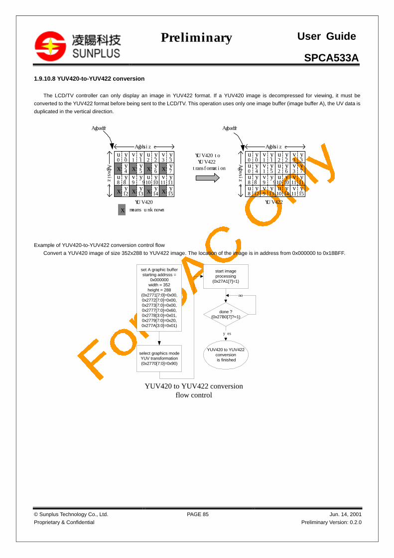
SPCA533A
© Sunplus Technology Co., Ltd.
Proprietary & Confidential
PAGE 85 Jun. 14, 2001
Preliminary Version: 0.2.0
Preliminary User Guide
1.9.10.8 YUV420-to-YUV422 conversion
The LCD/TV controller can only display an image in YUV422 format. If a YUV420 image is decompressed for viewing, it must be
converted to the YUV422 format before being sent to the LCD/TV. This operation uses only one image buffer (image buffer A), the UV data is
duplicated in the vertical direction.
YUV420 to YUV422 transformation
u0 0yv1 1yu2 2yv3 3y
4y
5y
6y
7y
u8 8yv9 9yu10 10yv11 11y
12y
13y
14y
15y
u0
v1
u2
v3
u8
v9
u10
v11
x
x x x x
x x x x
u0 0yv1 1yu2 2yv3 3y
4y
5y
6y
7y
u8 8yv9 9yu10 10yv11 11y
12y
13y
14y
15y
means unknown
YUV420 YUV422
Agbaddr Agbaddr
Agbvsize
Agbhsize AgbhsizeAgbvsize
Example of YUV420-to-YUV422 conversion control flow
Convert a YUV420 image of size 352x288 to YUV422 image. The location of the image is in address from 0x000000 to 0x18BFF.
done ?(0x27B0[7]?=1)
no
start imageprocessing
(0x27A1[7]=1)
set A graphic bufferstarting addrsss =
0x000000width = 352height = 288
(0x2771[7:0]=0x00,0x2772[7:0]=0x00,0x2773[7:0]=0x00,0x2777[7:0]=0x60,0x2778[3:0]=0x01,0x2779[7:0]=0x20,0x277A[3:0]=0x01)
yes
YUV420 to YUV422conversion is finished
YUV420 to YUV422 conversionflow control
select graphics modeYUV transformation(0x2770[7:0]=0x90)

SPCA533A
© Sunplus Technology Co., Ltd.
Proprietary & Confidential
PAGE 86 Jun. 14, 2001
Preliminary Version: 0.2.0
Preliminary User Guide
1.9.11 SDRAM space partition in different operation mode
The SDRAM space is partitioned to many regions during camera operation. The size of these regions can be very different among
applications. For example, a 3M CCD system and 1.4M CCD system have different sizes of the frame buffer. The locations of these regions
are programmable via the internal registers of the SDRAM controller. The following diagram demonstrates a typical SDRAM space partition
and the pointers (starting address of the regions). The following address pointer are used in the SDRAM controller of the SPCA533.
Afbaddr The starting address of A-frame buffer (the data of this buffer is YUV422/YUV420 foramt)
Bfbaddr The starting address of B-frame buffer (the data of this buffer is YUV422/YUV420 format)
Rfbaddr The starting address of the raw data frame buffer
VLCAstart The starting address of the first VLC stream
VLCBstart The starting address of the second VLC stream
TMBstart The starting address to save the thumbnail data (generated by the JPEG compression)
AUDstaddr The starting address of audio buffer
OSDaddr The OSD fonts database starting address
AGBaddr The starting address of A image buffer, used in the image process engine
BGBaddr The starting address of B image buffer, used in the image process engine
The following diagram shows an example of the SDRAM space allocation. Some of the partitions are not explicitly pointed by a pointer. But
they are necessay in a practically allocation.
SDRAM space partition for 3M(2048X1536) sensor
Bad pixel coordinates1024
Display area640x480x2=614400
FontOSD32768
Graphic OSD512x1024=524288
FAT131072
VideoClip_VLC_A320x240/4=19200
VideoClip_VLC_B320x240/4=19200
JPEG DC-term256x192=49152
Thumbnail160x120=19200
Thumbnail_VLC160x120/4=4800
AudioBuffer4096
main_frame_buffer_A2064x1542=3182688
main_frame_buffer_B2064x1542=3182688
Free area
Bad pixel coordinate format
X-coordinate 0Y-coordinate 0X-coordinate 1Y-coordinate 1X-coordinate 2Y-coordinate 2X-coordinate 3Y-coordinate 3
.....
.....
.....00
X-coordinate NY-coordinate N
0
00
.....
.....
0123456
10231022
7
16-bit
256MBits SDRAM space allocation
320x240
640x480
640x480
configuration 1, for LCD image playbackSetup menu
Display buffer
configuration 2,for TV image playback
Font-based OSD format
font 0
font 1
font 2
font 3
font 511
64word
Graphic-based OSD
512x1024(image)
320x240
320x240
320x240
320x240
320x240
320x240
320x240
16 M
wor
ds S
DR
AM
(25
6MB
its)
7.5M
wor
ds
afbaddr
bfbaddr
tmbstart
vlcastart
vlcbstart
audstart
osdstart

SPCA533A
© Sunplus Technology Co., Ltd.
Proprietary & Confidential
PAGE 87 Jun. 14, 2001
Preliminary Version: 0.2.0
Preliminary User Guide
PREVIEW mode :
Two frame buffers are needed while the camera is operating in the Preview mode. The double is required for the frame rate conversion if
the sensor frame rate is different from the LCD(TV) frame rate. The data in the frame buffers are in YUV422 format. The image data from the
sensors are processed and written into the A/B frame buffer sequencially. While the image data is written into the A-frame buffer, the data in
the B-frame buffer is read out for display. While the data is written into the B-frame buffer, the data in the A-frame buffer is read out for
display.
afbaddr
bfbaddr
image from the sensor
image to the LCD
A-frame buffer
B-frame buffer
SDRAM
afbaddr
bfbaddr
image from the sensor
image to the LCDA-frame buffer
B-frame buffer
SDRAM
PC-CAM mode :
The LCD(TV) interface should be turned off in the PC-Cam mode. Only A-frame buffer is required. If the USB bandwidth is notsufficient to transmit the image at the input frame rate, the SPCA533A drops frames when necessary. The data in the A-frame buffer couldbe raw data or the YUV422 data, depending on the imgtype selection.
A-framebuffer
afbaddr
image from the sensorimage to the LCD
Snap a single image :
Snapping a single image requires three buffers. The first one is the raw data buffer which is used to hold the raw data from the sensor.
After bad-pixel concealment, the raw data is sent to the CDSP for color processing. The output of the CDSP is written back to the A-frame
buffer in the SDRAM. Then JPEG compression is performed on the YUV422 format data. The compressed data (VLC stream) is written into
the B-frame buffer. After compression, the file header and the compressed thumbnail image is saved in front of the VLC stream to construct
an EXIF2.1 JPEG file.

SPCA533A
© Sunplus Technology Co., Ltd.
Proprietary & Confidential
PAGE 88 Jun. 14, 2001
Preliminary Version: 0.2.0
Preliminary User Guide
vlcstart
construct the EXIF2.1 file
EXIF2.1 fileDMA storage media
rfbaddr
LCD display
capture raw data Color processingH-scale down for the display device
compression
A frame buffer(raw data)
A frame buffer(raw data)
B frame buffer (YUV422 image)
rfbaddr
bfbaddr
A frame buffer (H-scaled image)
B frame buffer (YUV422 image)
bgbaddr
H-scaled image
YUV422 image
V-scale down for the display device
agbaddr
agbaddr
bgbaddr(afbaddr)
VLC stream
YUV422 image
bfbaddr
vlcaddr
display buffer (V-scaled image)
display buffer (V-scaled image)
LCD display
afbaddr
VLC stream
YUV422 image
display buffer (V-scaled image)
LCD display
afbaddr(agbaddr)
Generate thumbnail(scale down)
thumbnail YUV422(thumbnail buffer)
bgbaddr
VLC stream
YUV422 image
display buffer (V-scaled image)
LCD display
afbaddr(agbaddr)
Generate thumbnail(scale down)
thumbnail YUV422(thumbnail buffer)
bfbaddr
thumbnail(thumbnail_vlc buffer)
VLC stream
YUV422 image
display buffer (V-scaled image)
thumbnail(thumbnail_vlc buffer)
header
thumbnail VLC
header

SPCA533A
© Sunplus Technology Co., Ltd.
Proprietary & Confidential
PAGE 89 Jun. 14, 2001
Preliminary Version: 0.2.0
Preliminary User Guide
Continuous shot :
The continuous shot is also performed in the DSC mode. The number of pictures taken in a continuous shot is determined by register
snapnum (0X2B05). The raw image data is stored in the SDRAM raw data buffer, which is pointed by rfbaddr register (0X2768 ~ 0X276A) .
The maximum number of pictures that can be taken in a continuous shot is limited by the capacity of the SDRAM. After all the raw data is
captured, the data is processed frame by frame. This includes the color processing, compression and file saving. The following diagram
demonstrates the operation flow and the SDRAM space allocation.
3Mx16 raw dataframe buffer
3Mx16 raw dataframe buffer
3Mx16 raw dataframe buffer
rfbaddr3Mx16 raw dataframe buffer
3Mx16 raw dataframe buffer
3Mx16 raw dataframe buffer
80x60 YUV80x60 YUV80x60 YUV
Display buffer(280x220)
afbaddrLCDdisplay
3Mx16 raw dataframe buffer
3Mx16 raw dataframe buffer
3Mx16 raw dataframe buffer
afbaddr
BFB(2048x1536)
bfbaddr
2Mx16 raw dataframe buffer
2Mx16 raw dataframe buffer
2Mx16 raw dataframe buffer
BFB(2048x1536)
bfbaddr
VLC FIFO(2048x1536/3)
storage media
step 1:capture raw data
step 2:interpolation and scale down
step 3:paste to display buffer to show on
LCD
step 4:interpolate and store to BFB
step 5:compress to VLC FIFO and DMA
repeat 3 times
Continuous Shot SDRAM partition
repeat 3 times
2Mx16 raw dataframe buffer
80x60 YUV80x60 YUV80x60 YUV
3Mx16 raw dataframe buffer
3Mx16 raw dataframe buffer
3Mx16 raw dataframe buffer
Display buffer(280x220)
LCDdisplay
afbaddrDisplay buffer(280x220)
LCDdisplay
vlcstart
DMA
VIDEOCLIP :
The SPCA533A can capture the video and audio data at the same time. The captured data is tailored and format to an AVI file. In
videoclip, two frame buffers, two VLC buffers and one audio buffer are allocated. Dual frame buffer allows the SPCA533A to perform the
frame rate conversion during the videoclip. The size of the audio buffer is porgammabl. It could be 1K, 2K, 4K or 8K bytes.

SPCA533A
© Sunplus Technology Co., Ltd.
Proprietary & Confidential
PAGE 90 Jun. 14, 2001
Preliminary Version: 0.2.0
Preliminary User Guide
dmaaddr
Frame Buffer A320x240
Frame Buffer B320x240
VLC Buffer A320x240x1.5/4
VLC Buffer B320x240x1.5/4
Audio Buffer1K,2K,4K,8K
afbaddr
bfbaddr
vlcastart
vlcbstart
audstart
audio data> 1K
set Vidclip mode
vlcardy orvlcbrdy?
NO
NO
DMA AVI header(8 bytes)
DMA VLC data tostorage media
YES
DMA AVI header(8 bytes)
DMA AUDIO data tostorage media
YES
set vlcardy or vlcbrdyto 0
PLAY BACK mode :
Because it takes longer time to decompress and playback a large size image on the LCD, the user may decompress the thumbnail to
reduce the playback time. The decompressed thumbnail data is put in the display buffer first, then turn on the LCD to show the thumbnail.
After that, the primary image can be loaded to the SDRAM and decompressed to another display buffer. Up to this step, the primary image is
in the frame buffer B. But this image size is too large to show on the LCD. So it is recommended to scale down the primary image to the size
fitting to show on the LCD. After that, program the “lcdsrcidx” to one to show this image.
The following diagram illustrates the procedure of playback a single image.

SPCA533A
© Sunplus Technology Co., Ltd.
Proprietary & Confidential
PAGE 91 Jun. 14, 2001
Preliminary Version: 0.2.0
Preliminary User Guide
thumbnail VLC
step 2decompress thumbnail
step1load thumbnail
VLC
DMA
thumbnail(Display buffer)
afbaddr
thumbnail VLC image VLCDMA image VLC
BFB2048x1536
bfbaddr
BFB2048x1536
agbaddr
280x1536
step 3load image VLC
step 4decompress image
step 5h-scale down
LCD display
DMAstaddr DMAstaddr
bgbaddr
bgbaddr(bfbaddr)
280x1536
step 6v-scale downand show image
agbaddr
LCD display
thumbnail(Display buffer)
afbaddr
thumbnail(Display buffer)
afbaddr
LCD display
LCD display
thumbnail(Display buffer)
afbaddrLCD displaythumbnail
(Display buffer)
Image(Display buffer)
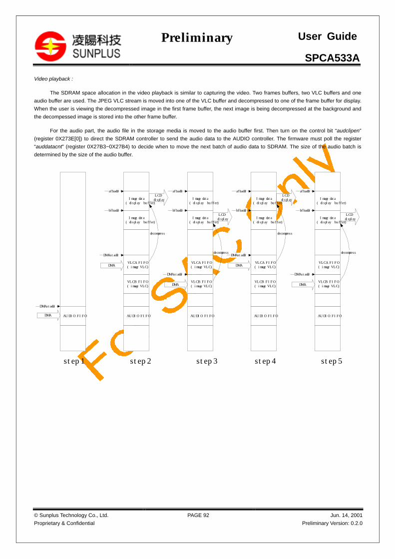
SPCA533A
© Sunplus Technology Co., Ltd.
Proprietary & Confidential
PAGE 92 Jun. 14, 2001
Preliminary Version: 0.2.0
Preliminary User Guide
Video playback :
The SDRAM space allocation in the video playback is similar to capturing the video. Two frames buffers, two VLC buffers and one
audio buffer are used. The JPEG VLC stream is moved into one of the VLC buffer and decompressed to one of the frame buffer for display.
When the user is viewing the decompressed image in the first frame buffer, the next image is being decompressed at the background and
the decompessed image is stored into the other frame buffer.
For the audio part, the audio file in the storage media is moved to the audio buffer first. Then turn on the control bit “audclipen”
(register 0X273E[0]) to direct the SDRAM controller to send the audio data to the AUDIO controller. The firmware must poll the register
“auddatacnt” (register 0X27B3~0X27B4) to decide when to move the next batch of audio data to SDRAM. The size of the audio batch is
determined by the size of the audio buffer.
Image data(display buffer)
VLCB FIFO (image VLC)
AUDIO FIFO
afbaddr
DMA
DMAstaddr
VLCA FIFO(image VLC)
Image data(display buffer)
bfbaddr
decompress
LCD display
AUDIO FIFODMA
DMAstaddr
step 1 step 2 step 3
Image data(display buffer)
VLCB FIFO (image VLC)
AUDIO FIFO
afbaddr
DMA
DMAstaddr
VLCA FIFO(image VLC)
Image data(display buffer)
bfbaddr
decompress
LCD display
Image data(display buffer)
VLCB FIFO (image VLC)
AUDIO FIFO
afbaddr
DMA
DMAstaddr
VLCA FIFO(image VLC)
Image data(display buffer)
bfbaddr
decompress
LCD display
step 4 step 5
Image data(display buffer)
VLCB FIFO (image VLC)
AUDIO FIFO
afbaddr
DMA
DMAstaddr
VLCA FIFO(image VLC)
Image data(display buffer)
bfbaddr
decompress
LCD display

SPCA533A
© Sunplus Technology Co., Ltd.
Proprietary & Confidential
PAGE 93 Jun. 14, 2001
Preliminary Version: 0.2.0
Preliminary User Guide
audio data< 1K
set Playback mode
NO
DMA AVI header toCPU(8 bytes)
DMA VLC data toSDRAM(VLCA or VLCB)
DMA AVI header toCPU(8 bytes)
DMA AUDIO data toSDRAM
YES
change LCD display index(Frame Buffer A or B)
YES
polling decompress done?
YES
polling LCD Vsync
NO
NO
set start decompress
1.10 Serial interface
The SPCA533A supports two types of serial interfaces. The first type is synchronous serial interface, and the other type is three-wire
serial interface. Synchronous serial interface (SSC) is usually used to control a TV decoder or CMOS sensors. The three-wire serial
interface is usually used to program the registers of a CDSAGC used in a CCD camera system.
1.10.1 Synchronous Serial interface (SSC)
The synchronous serial interface has a data pin and a clock pin. The clock pin is driven by the SPCA533A and the data pin is a bi-
directional pin. Both pins are pulled-up by external resistors. Before using the SSC to program the CMOS sensors (or TV decoders), the
clock frequency on the clock pin must be determined. It is programmable via registers 0X2904. The SSC of the SPCA533A supports several
types of protocol as described below.
Normal write protocol In this mode, the sub-address of the CMOS sensor is transmitted only once. This sub-addressusually represents which register in the CMOS sensors is to be programmed. Register 0x2905[3:0] determines how manybytes are to be transmitted to the CMOS sensor. The maximum number of bytes in a single transmission is 16 bytes. If theCMOS sensor supports linear sub-address increment, the SPCA533A can write several bytes of data to the CMOS sensor ina single transmission. The transmission is started right after the last data register is written. For example, if the write count is2, the SPCA533A will start transmission once DATA1 register is written. There might be some side effects if the CMOSsensor’s registers are programmed in the middle of an image frame. For example, changing the gain registers might causedifferent gain values in the same frame of data. The SPCA533A is able to delay the serial interface programming until thestart of the next frame. To do this, register 0X2903[0] must be set to 1.Normal write control flow
S Slave Address + wbACKs DATAn(WR_COUNT)ACKsSUB Address ACKs DATA0 ACKs P
(Note: S represents the start bit and P represents the stop bit)

SPCA533A
© Sunplus Technology Co., Ltd.
Proprietary & Confidential
PAGE 94 Jun. 14, 2001
Preliminary Version: 0.2.0
Preliminary User Guide
Setting the mode to SSC normal mode (0x2901[1:0] = 2'b00)
Setting the Slave Address (0x2900[7:0])
Setting the Register Address0 (0x2910)
Setting the Wrcount (0x2905[3:0])
the max value is 0 (16 bytes), mean the number of byte to transfer
updatevd ? (0x2025[0]) ?= 1
Yes
Wait Vsync falling edge
No
Trigger SSC normal write
SSC normal writeFinished
Done ?(0x29A0[0]) ? = 0
Sync with Vd ? (0x2903[0]) ?= 1
Yes
No
No
Yes Write the Data register DATA0 (0x2911) DATA1 (0x2913)
. DATAn
(n = Wrcount - 1)
Normal write flow chart
Burst write protocol This mode allows the user to write several bytes of data to the CMOS sensors in a single transmission,each byte with a different sub-address. The burst write transmission can also be delayed to the start of the next image frame.
S Slave Address + wbACKs Burst_addr0ACKs DATA0 ACKs P S Slave Address + wbACKs Burst_addrn( WR_COUNT)ACKs DATAn(WR_COUNT)ACKs P

SPCA533A
© Sunplus Technology Co., Ltd.
Proprietary & Confidential
PAGE 95 Jun. 14, 2001
Preliminary Version: 0.2.0
Preliminary User Guide
Setting the mode to SSC Burst mode
(0x2901[1:0] = 2'b01)
Setting the Slave Address (0x2900)
Setting the Register Address 0 (0x2910)Address 1 (0x2912)
.Address n
(n = Wrcount - 1)
Setting the Wrcount (0x2905[3:0])
the max value is 0 (16 bytes), mean the number of byte to transfer
updatevd ? (0x2025[0]) ?= 1
Yes
Wait Vsync falling edge
No
Trigger SSC Burst write
SSC Burst writeFinished
Done ?(0x29A0[0]) ? = 0
Sync with Vd ? (0x2903[0]) ?= 1
Yes
No
No
Yes
Write the Data register DATA0 (0x2911) DATA1 (0x2913)
. DATAn
(n = Wrcount - 1)
Burst write flow chart
Data read protocol The SPCA533A supports three types of read protocols as shown below. Depending on the CMOSsensors, the users may select any of these protocols that most fit the CMOS sensors’ requirement. The first protocol is thebasic type. It sends a stop code before any start code. The second one omits the stop code. And the last one omits the sub-address field. All these types of read require the CMOS sensor to support the linear address increment. Again, the readtransmission can be delayed to the start of the next frame. However, this is usually not necessary.
The basic data read protocol: (Rstarten = 0 & Subaddren= 1)S Slave Address + wbACKs SUB Address ACKsP S Slave Address + rdACKs DATA0 ACKm DATAn( RD_COUNT)~ACKmP
The data read protocol with restart code: (Rstarten = 1 & Subaddren = 1)S Slave Address + wbACKs SUB AddressACKs S Slave Address + rdACKs DATA0 ACKm DATAn( RD_COUNT)~ACKmP
The data read protocol without the sub-addressS Slave Address + rdACKs DATA0 ACKm DATAn( RD_COUNT)~ACKmP

SPCA533A
© Sunplus Technology Co., Ltd.
Proprietary & Confidential
PAGE 96 Jun. 14, 2001
Preliminary Version: 0.2.0
Preliminary User Guide
updatevd ? (0x2025[0]) ?= 1
Yes
Wait Vsync falling edge
No
Trigger SSC Read
Cpu can read data from data registers
Done ?(0x29A0[0]) ? = 0
Sync with Vd ? (0x2903[0]) ?= 1
Yes
No
No
Yes
Setting the mode to SSC normal mode(0x2901[1:0] = 2'b00)
Setting the Slave Address (0x2900)
Subaddren ? (0x2902[0]) ?=1
Yes
Set Rstarten bit to enable restart function or not
(0x2902[1])
Setting the Register Address 0 (0x2910)
Set Rdcount (0x2905[7:4])
the max value is 0 (16 bytes), mean the number of byte to transfer
No
Set the Prefetch bit (0x2902[4])
SSC read flow chart
1.10.2 Three-wire interface
SPCA533A supports 4 types of three-wire protocols. These protocols conform to the most frequently used CDSAGC chips in a CCD
camera system. In the application, this interface can only write register values to the CDSAGC but not read from them. Like the SSC, the
clock frequency has to be selected before using the three-wire serial interface. Register 0x2504[7:0] determines the clock frequency used in
transmission. The SPCA533A can transmit up to 80 bits to the CDSAGC in a single transmission. However, the real number of bits
acceptable is determined by the CDSAGC. The users have to pay attention to the bit-sequence of transmission. The SPCA533A transmits
low byte first and LSB first. Refer to the following diagram. The bit 0 of the DATA0 is the first bit to be sent to the CDSAGC.
DATA0 (Bit0)DATA0 (Bit1)DATA0 (Bit2) DATAn (Bitn-1)DATAn (Bitn)
The Total Bits is CDS_BITS
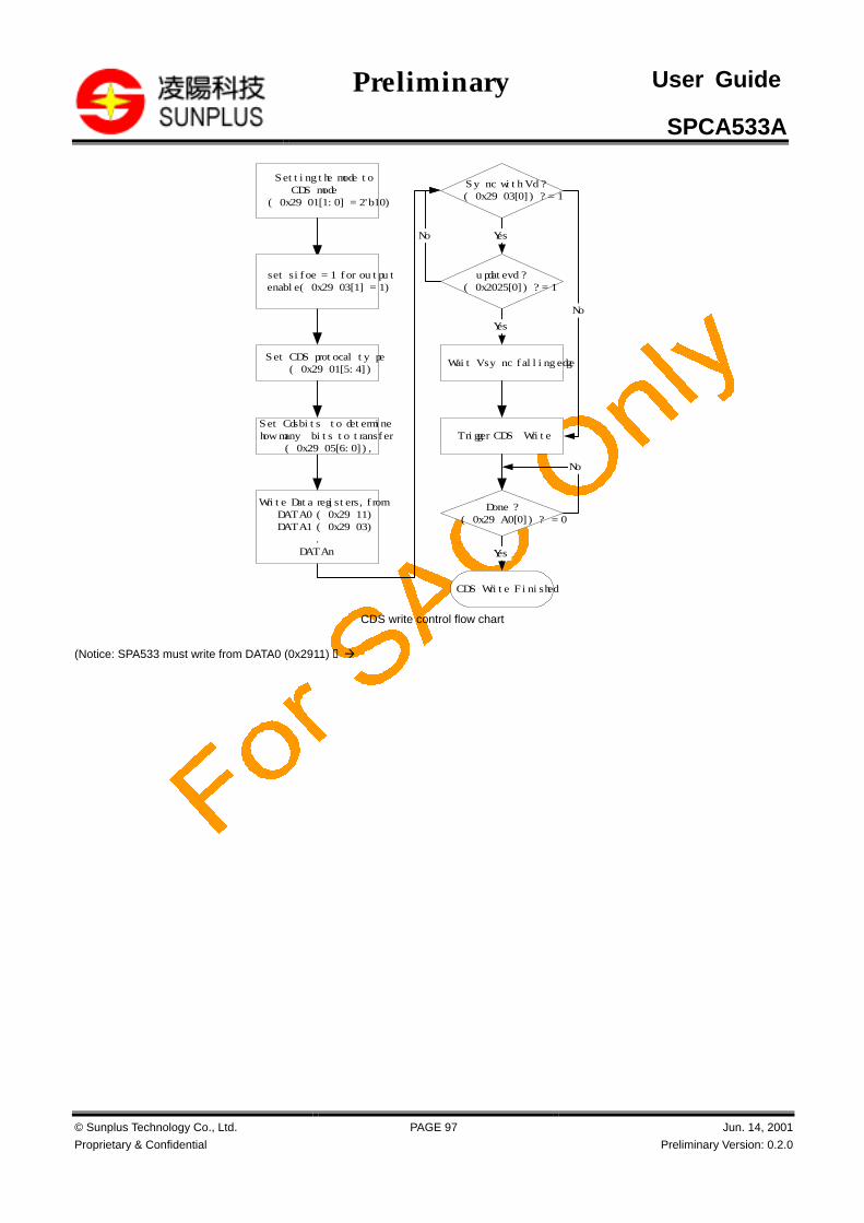
SPCA533A
© Sunplus Technology Co., Ltd.
Proprietary & Confidential
PAGE 97 Jun. 14, 2001
Preliminary Version: 0.2.0
Preliminary User Guide
updatevd ? (0x2025[0]) ?= 1
Yes
Wait Vsync falling edge
No
Trigger CDS Write
CDS Write Finished
Done ?(0x29A0[0]) ? = 0
Sync with Vd ? (0x2903[0]) ?= 1
YesNo
No
Yes
Setting the mode to CDS mode
(0x2901[1:0] = 2'b10)
set sifoe = 1 for output enable(0x2903[1] = 1)
Write Data registers, from DATA0 (0x2911)DATA1 (0x2903)
.DATAn
Set CDS protocal type (0x2901[5:4])
Set Cdsbits to determine how many bits to transfer
(0x2905[6:0]),
CDS write control flow chart
(Notice: SPA533 must write from DATA0 (0x2911) DATA1 (0x2903) ….. DATAn, when write the number of Data
register bits >= Cdsbits, the three-wire interface will trigger to send out data.
EX: If you setting the Cdsbits is 19, then when you write DATA0 DATA1 DATA2, then the three wire interface will send
out the data)
The SPCA533A supports 4 types of serial timing in the three-wired protocol. The type can be set in register 0x2901[5:4].
Type 0 timing (for SHARP Family CDSAGC chips)
Last falling edge of SCK must latch SDATA@HIG
SCK
SD
Cdsbits = 0x0A, DATA0 = 0x55, DATA1 = 0xAA
Type 1 timing (for HITACHI HD49322F, ADI AD9803, EXAR XRD44L61/2 chips)
SCK
SD
SEN
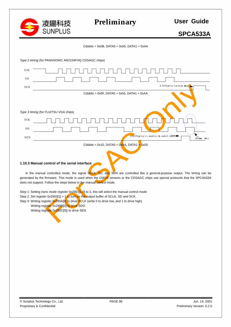
SPCA533A
© Sunplus Technology Co., Ltd.
Proprietary & Confidential
PAGE 98 Jun. 14, 2001
Preliminary Version: 0.2.0
Preliminary User Guide
Cdsbits = 0x0B, DATA0 = 0x55, DATA1 = 0xAA
Type 2 timing (for PANASONIC AN2104FHQ CDSAGC chips)
SCK
SD
SEN A SEN pulse latch the data
Cdsbits = 0x0F, DATA0 = 0x55, DATA1 = 0xAA
Type 3 timing (for FUJITSU VGA chips)
SCK
SD
SEN A SEN pulse is need in the end of transfer
Dummy data
Cdsbits = 0x10, DATA0 = 0xAA, DATA1 = 0x55
1.10.3 Manual control of the serial interface
In the manual controlled mode, the signal SCLK, SD, and SEN are controlled like a general-purpose output. The timing can be
generated by the firmware. This mode is used when the CMOS sensors or the CDSAGC chips use special protocols that the SPCA533A
does not support. Follow the steps below in the manual control mode.
Step 1: Setting trans mode register 0x2901[1:0] to 3, this will select the manual control mode
Step 2. Set register 0x2903[1] = 1 to turn on the output buffer of SCLK, SD and SCK.
Step 3: Writing register 0x290A[0] to drive SCLK (write 0 to drive low, and 1 to drive high)
Writing register 0x290B[0] to drive SDO
Writing register 0x290C[0]) to drive SEN
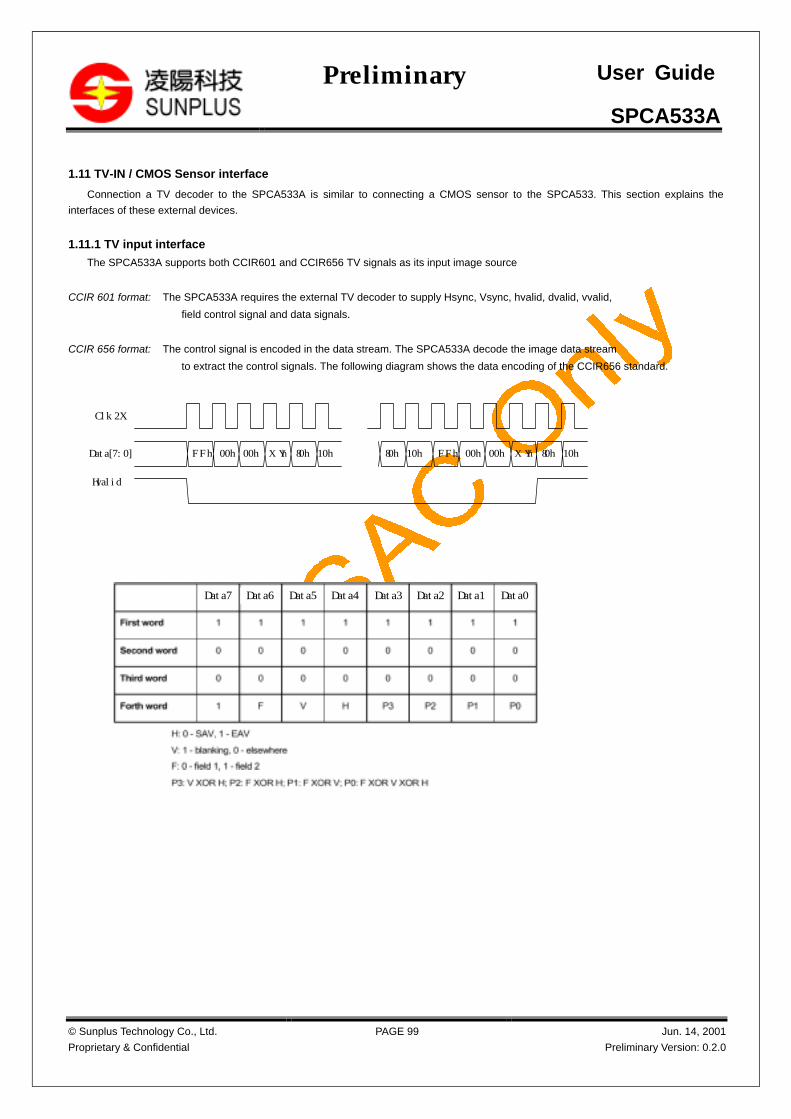
SPCA533A
© Sunplus Technology Co., Ltd.
Proprietary & Confidential
PAGE 99 Jun. 14, 2001
Preliminary Version: 0.2.0
Preliminary User Guide
1.11 TV-IN / CMOS Sensor interface
Connection a TV decoder to the SPCA533A is similar to connecting a CMOS sensor to the SPCA533. This section explains the
interfaces of these external devices.
1.11.1 TV input interface
The SPCA533A supports both CCIR601 and CCIR656 TV signals as its input image source
CCIR 601 format: The SPCA533A requires the external TV decoder to supply Hsync, Vsync, hvalid, dvalid, vvalid,
field control signal and data signals.
CCIR 656 format: The control signal is encoded in the data stream. The SPCA533A decode the image data stream
to extract the control signals. The following diagram shows the data encoding of the CCIR656 standard.
Data7Data6Data5Data4Data3Data2Data1Data0
FFh 00h 00hXYh FFh 00h 00hXYh80h 10h80h 10h 80h 10h
Clk2X
Data[7:0]
Hvalid
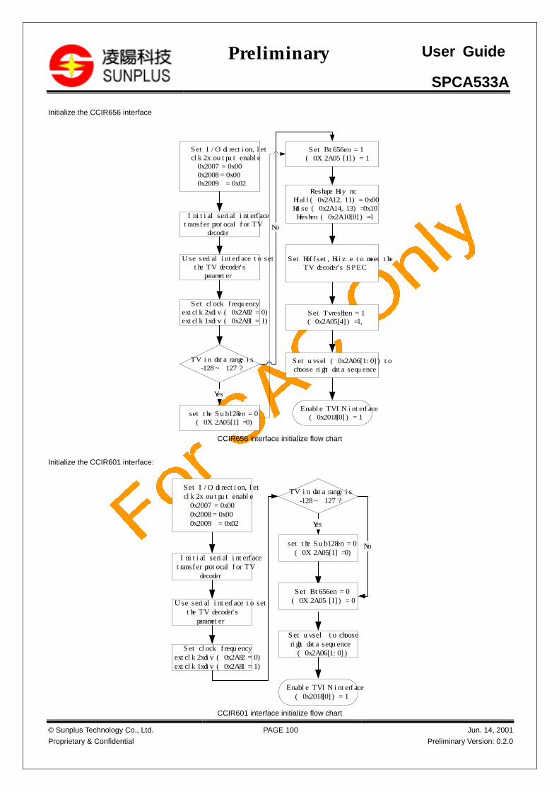
SPCA533A
© Sunplus Technology Co., Ltd.
Proprietary & Confidential
PAGE 100 Jun. 14, 2001
Preliminary Version: 0.2.0
Preliminary User Guide
Initialize the CCIR656 interface
Enable TVIN interface (0x2018[0]) = 1
Set I/O direction, let clk2x output enable0x2007 = 0x000x2008 = 0x000x2009 = 0x02
Set clock frequencyextclk2xdiv (0x2A82 = 0)extclk1xdiv (0x2A81 = 1)
TV in data range is -128 ~ 127 ?
Yes
Reshape HsyncHfall(0x2A12, 11) = 0x00 Hrise (0x2A14, 13) =0x10 Hreshen (0x2A10[0]) =1
set the Sub128en = 0(0X2A05[1] =0)
Set Bt656en = 1(0X2A05 [1]) = 1
Set Hoffset, Hsize to meet the TV decoder's SPEC
Set Tvreshhen = 1(0x2A05[4]) =1,
Set uvsel (0x2A06[1:0]) to choose right data sequence
Initial serial interface transfer protocal for TV
decoder
Use serial interface to set the TV decoder's parameter
No
CCIR656 interface initialize flow chart
Initialize the CCIR601 interface:
Enable TVIN interface (0x2018[0]) = 1
Set I/O direction, let clk2x output enable0x2007 = 0x000x2008 = 0x000x2009 = 0x02
Set clock frequencyextclk2xdiv (0x2A82 = 0)extclk1xdiv (0x2A81 = 1)
TV in data range is -128 ~ 127 ?
Yes
Set uvsel to choose right data sequence(0x2A06[1:0])
set the Sub128en = 0(0X2A05[1] =0)
Initial serial interface transfer protocal for TV
decoder
Use serial interface to set the TV decoder's parameter
No
Set Bt656en = 0(0X2A05 [1]) = 0
CCIR601 interface initialize flow chart

SPCA533A
© Sunplus Technology Co., Ltd.
Proprietary & Confidential
PAGE 101 Jun. 14, 2001
Preliminary Version: 0.2.0
Preliminary User Guide
Data sequence: The order bits in register uvsel (0X2906) is used to select one of the data sequence
Y0 Cb0 Y1 Cr0 Y2 Cb1 Y3
Y0 Cr0 Y1 Cb0 Y2 Cr1 Y3 Cb1 Y4Cb2
Cr1 Y0 Cb2
Uvsel = 2'b01After interplation : Cbout = Cb, Yout = Y_1d, Crout = Cr_2d
Uvsel = 2'b11After interplation : Cbout = Cb_2d, Yout = Y_1d, Crout = Cr
Y0 Cb0 Y1 Cr0 Y2 Cb1 Y3
Y0 Cr0 Y1 Cb0 Y2 Cr1 Y3 Cb1 Y4Cb2
Cr1 Y0 Cb2
Uvsel = 2'b01After interplation : Cbout = Cb, Yout = Y_1d, Crout = Cr_2d
Uvsel = 2'b11After interplation : Cbout = Cb_2d, Yout = Y_1d, Crout = Cr
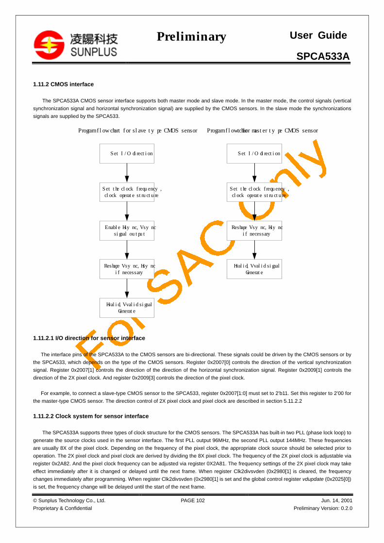
SPCA533A
© Sunplus Technology Co., Ltd.
Proprietary & Confidential
PAGE 102 Jun. 14, 2001
Preliminary Version: 0.2.0
Preliminary User Guide
1.11.2 CMOS interface
The SPCA533A CMOS sensor interface supports both master mode and slave mode. In the master mode, the control signals (vertical
synchronization signal and horizontal synchronization signal) are supplied by the CMOS sensors. In the slave mode the synchronizations
signals are supplied by the SPCA533.
Program flow chart for slave type CMOS sensor Program flow chart for master type CMOS sensor
Set the clock frequency, clock operate structure
Reshape Vsync, Hsyncif necessary
Set I/O direction
Enable Hsync, Vsync signal output
Hvalid, Vvalid signal Generate
Set the clock frequency, clock operate structure
Reshape Vsync, Hsyncif necessary
Set I/O direction
Hvalid, Vvalid signal Generate
1.11.2.1 I/O direction for sensor interface
The interface pins of the SPCA533A to the CMOS sensors are bi-directional. These signals could be driven by the CMOS sensors or by
the SPCA533, which depends on the type of the CMOS sensors. Register 0x2007[0] controls the direction of the vertical synchronization
signal. Register 0x2007[1] controls the direction of the direction of the horizontal synchronization signal. Register 0x2009[1] controls the
direction of the 2X pixel clock. And register 0x2009[3] controls the direction of the pixel clock.
For example, to connect a slave-type CMOS sensor to the SPCA533, register 0x2007[1:0] must set to 2’b11. Set this register to 2’00 for
the master-type CMOS sensor. The direction control of 2X pixel clock and pixel clock are described in section 5.11.2.2
1.11.2.2 Clock system for sensor interface
The SPCA533A supports three types of clock structure for the CMOS sensors. The SPCA533A has built-in two PLL (phase lock loop) to
generate the source clocks used in the sensor interface. The first PLL output 96MHz, the second PLL output 144MHz. These frequencies
are usually 8X of the pixel clock. Depending on the frequency of the pixel clock, the appropriate clock source should be selected prior to
operation. The 2X pixel clock and pixel clock are derived by dividing the 8X pixel clock. The frequency of the 2X pixel clock is adjustable via
register 0x2A82. And the pixel clock frequency can be adjusted via register 0X2A81. The frequency settings of the 2X pixel clock may take
effect immediately after it is changed or delayed until the next frame. When register Clk2divsvden (0x2980[1] is cleared, the frequency
changes immediately after programming. When register Clk2divsvden (0x2980[1] is set and the global control register vdupdate (0x2025[0])
is set, the frequency change will be delayed until the start of the next frame.

SPCA533A
© Sunplus Technology Co., Ltd.
Proprietary & Confidential
PAGE 103 Jun. 14, 2001
Preliminary Version: 0.2.0
Preliminary User Guide
Type 1: The SPCA533A supplies 2X pixel clock to the sensor, and the sensor returns the pixel clock. The register setting is
described below. The SPCA533A samples the sensors’ data with the clock output from the CMOS sensors.
Set TGPLLen (0x2080) , select 96MHz/144MHz clock source
Set Extclk2xdiv (0x2A82), 2X pixel clock frequency= the source clock frequency/ (Extclk2xdiv +1)
Set clk2x output enable (0x2009[1]) = 1,enable 2X pixel clock output
Set clk1x input (0x2009[3]) = 0, set the pixel clock as input
Set SelectTG1xCk (0x2019[7]) = 0, select pixel clock from the PAD
The frequency of the 2X pixel clock is adjustable via register 0x2A82. For example, TGPLLen = 0, Extclk2xdiv = 7, then clk2x = 96 / (7+1)
= 12MHz
Type 2: The SPCA533A supplied the pixel clock to the sensors and samples the data with the same clock. The register settings are
described below.
Set TGPLLen (0x2080), select 96MHz/144MHz clock source
SelectTG2xCk (0x2019[7]) = 1 select the internal 2X pixel clock source
Set Extclk2xdiv (0x2A82), 2X pixel clock frequency=source clock frequency / (Extclk2xdiv +1),
Set Extclk1xdiv (0x2A81), pixel clock frequency=2X pixel clock frequency/ (Extclk1xdiv + 1),
Set clk1x output (0x2009[3]), enable the pixel clock output
Type 3: Special mode for the HP CMOS sensor
The HP CMOS sensors provide “DRDY” signal for the backend system to sample the data. But this signal is paused during the blanking
period of a line. The SPCA533A accepts only periodic clock source. In this case, the pixel clock must be generated internally. The
SPCA533A automatically generates a periodical pixel clock, which is synchronized to the “DRDY” signal. The register settings are
described below.
Set TGPLLen (0x2080) select the144MHz/96MHz clock source
Set Extclk2xdiv (0x2A82) set the 2X pixel clock frequency
Set Extclk1xdiv (0x2A81), set the pixel clock frequency
Set Hpen (0x2A80[0]) = 1 enable the HP CMOS sensor mode
Set (0x2009[1]) = 1, set the 2X pixel clock as output pin
Set (0x2009[3]) = 0, set the pixel clock as input pin
Set (0x2019[7]) = 1, select the clock generator as the source of the pixel clock
The following diagram shows the clock routing of the CMOS sensor interface. Besides the function of the CCD’s driving
clocks, the ADCLP and ADCK pins are used as the clocks pins in a CMOS sensor system. In a CMOS sensor system, The ADCLP pin is
used as the 2X pixel clock and the ADCK is used as the pixel clock.
The 2X pixel clock has two sources. The first one is from the IO pad and the other one is from the internal clock generator. The source of
2X pixel clock is selected by register 0x2019[7]. The pixel clock has also two sources. One is from the IO pad; the other is from the internal
timing generator. This could be selected by register 0x2019[6].

SPCA533A
© Sunplus Technology Co., Ltd.
Proprietary & Confidential
PAGE 104 Jun. 14, 2001
Preliminary Version: 0.2.0
Preliminary User Guide
Clock Generation
Clk2xo
SelectTG2xCk (0x2019[7])
MUX
MUX
SelectTG1xCk (0x2019[6])
Clk1xo
Clk2xi
ADCLP PAD
ADCK PAD
adclp output enable (0x2009[1])
adclp output enable (0x2009[1])
Clk8x
0
1
0
1
MUXTvdecen (0x2018[0])
10
MUX
96MHz144MHz
TGPLLen (0x2080)0127MHz
Phaseadjust
Phaseadjust
Vclk
Clk2x
1.11.2.3 Hsync, Vsync output signal generate:
For the slave-type CMOS sensor, the SPCA533A generates the vertical (and horizontal) synchronization signal according to the following
flow.
Set Lineblank, Linetotal Frameblank, Frametotal (0x2A34,33), (0x2A32,31)(0x2A38,37), (0x2A36,35)
Set Frameblankcntclk (0x2A30[4]) to decide the Vsync blank is count from Hsync (0) or pixel clock (1)
Set Exthdopol (0x2A00[2]), Extvdopol (0x2A00[3]) to decide the output H-sync,
V-sync polarity
set Exthdoedge (0x2A00[4]) to decide the Hsync change in pixel clock rise edge(0) or negative edge(1)
Syncgenen (0x2A30[0]) = 1 to enable sync generator
The time period of a frame is determined by register Linetotal and Frametotal. Both registers, when changed, may take effect
immediately or until the start of the next frame. To delay the effective time, both register Totalsvden (0x2A30[1]) and vdupdate (0x2025[0])
must be set.
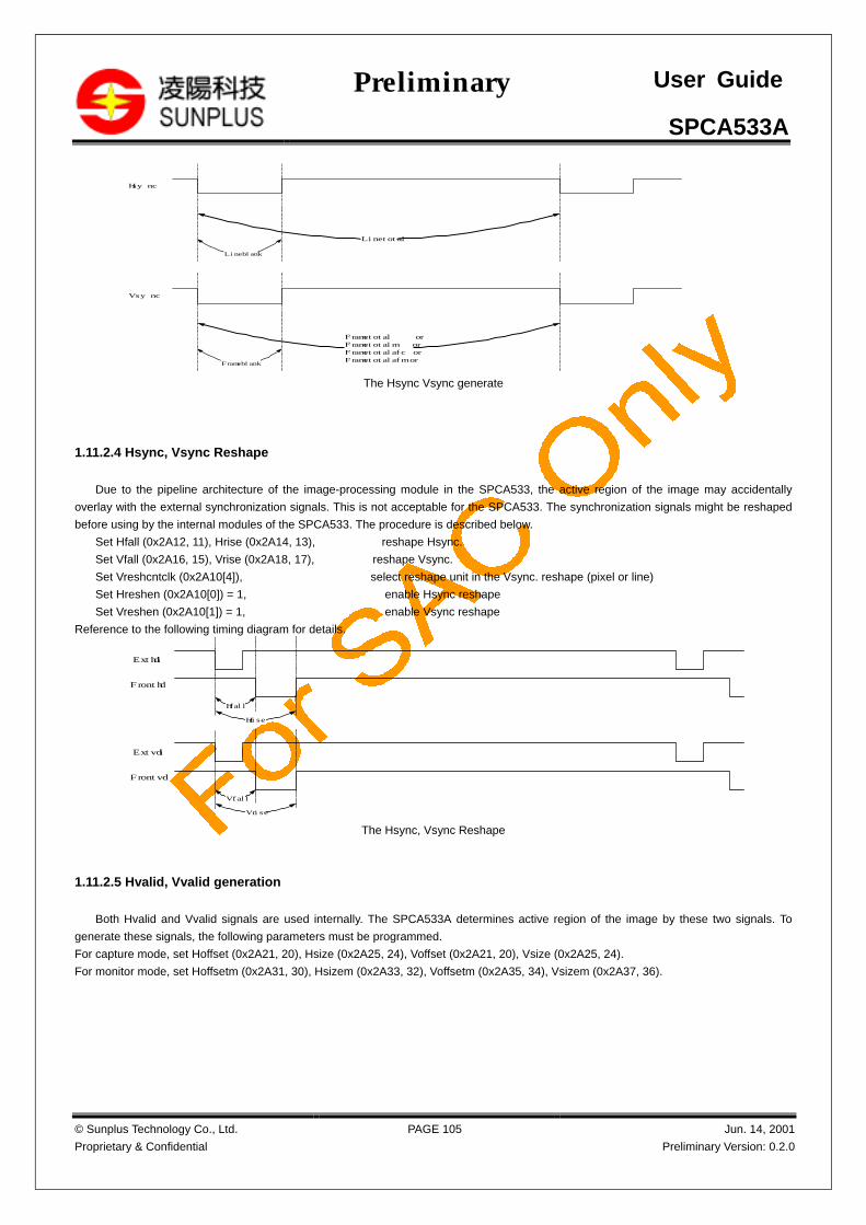
SPCA533A
© Sunplus Technology Co., Ltd.
Proprietary & Confidential
PAGE 105 Jun. 14, 2001
Preliminary Version: 0.2.0
Preliminary User Guide
Hsync
Linetotal
Lineblank
Vsync
Frametotal orFrametotalm orFrametotalafc orFrametotalafm or
Frameblank
The Hsync Vsync generate
1.11.2.4 Hsync, Vsync Reshape
Due to the pipeline architecture of the image-processing module in the SPCA533, the active region of the image may accidentally
overlay with the external synchronization signals. This is not acceptable for the SPCA533. The synchronization signals might be reshaped
before using by the internal modules of the SPCA533. The procedure is described below.
Set Hfall (0x2A12, 11), Hrise (0x2A14, 13), reshape Hsync.
Set Vfall (0x2A16, 15), Vrise (0x2A18, 17), reshape Vsync.
Set Vreshcntclk (0x2A10[4]), select reshape unit in the Vsync. reshape (pixel or line)
Set Hreshen (0x2A10[0]) = 1, enable Hsync reshape
Set Vreshen (0x2A10[1]) = 1, enable Vsync reshape
Reference to the following timing diagram for details.
Exthdi
Hfall
Fronthd
Hrise
Extvdi
Vfall
Frontvd
Vrise
The Hsync, Vsync Reshape
1.11.2.5 Hvalid, Vvalid generation
Both Hvalid and Vvalid signals are used internally. The SPCA533A determines active region of the image by these two signals. To
generate these signals, the following parameters must be programmed.
For capture mode, set Hoffset (0x2A21, 20), Hsize (0x2A25, 24), Voffset (0x2A21, 20), Vsize (0x2A25, 24).
For monitor mode, set Hoffsetm (0x2A31, 30), Hsizem (0x2A33, 32), Voffsetm (0x2A35, 34), Vsizem (0x2A37, 36).

SPCA533A
© Sunplus Technology Co., Ltd.
Proprietary & Confidential
PAGE 106 Jun. 14, 2001
Preliminary Version: 0.2.0
Preliminary User Guide
HoffsetHoffsetm
HsizeHsizem
Hsync data valid
VoffsetVoffsetmVoffsetafcVoffsetafm
VsizeVsizemVsizeafcVsizeafm
Vsync data valid
Exthdi
Extvdi
Hvalid
Vvalid
Valid signal generate
1.11.3 Image Capture:
Image capture flow in the master mode CMOS sensor is different from the one in the slave mode CMOS sensor. The following diagrams
show both control flows.
Master type CMOS sensor snap flow chart:
Snap Finished
Done ?(0x2B05[4]) ? = 0
Set Hoffset , Hsize Voffset, Vsize for capture mode
(0x2A21, 20), (0x2A25, 24)(0x2A23, 22), (0x2A27, 26)
Set Hoffsetm , Hsizem Voffsetm, Vsizem for capture mode
(0x2A31, 30), (0x2A32, 33)(0x2A35, 34), (0x37, 36)
Vd falling edge
Yes
No
To program CMOS sensor from Subsample
mode to full frame mode
Set the snaptrg (0x2B05[4]), and snapnum (0x2B05[3:0])
Yes
No
To program CMOS sensor from full frame mode to Subsample mode
Slave type CMOS sensor snap flow chart:

SPCA533A
© Sunplus Technology Co., Ltd.
Proprietary & Confidential
PAGE 107 Jun. 14, 2001
Preliminary Version: 0.2.0
Preliminary User Guide
Snap Finished
Done ?(0x2B05[4]) ? = 0
Set Hoffset , Hsize Voffset, Vsize for capture mode
(0x2A21, 20), (0x2A25, 24)(0x2A23, 22), (0x2A27, 26)
Set Hoffsetm , Hsizem Voffsetm, Vsizem for capture mode
(0x2A31, 30), (0x2A32, 33)(0x2A35, 34), (0x37, 36)
Vd falling edge
Yes
No
To program CMOS sensor from Subsample
mode to full frame mode
Set the snaptrg (0x2B05[4]), and snapnum (0x2B05[3:0])
Set Lineblank Linetotal Frameblank , Frametotalfor monitor mode
(0x2A34,33), (0x2A32,31)(0x2A38,37), (0x2A36,35)
Set Totalsvden(0x2940[1]) = 1
Set Lineblank Linetotal Frameblank , Frametotalfor capture mode
(0x2A34,33), (0x2A32,31)(0x2A38,37), (0x2A36,35)
Set Lineblank Linetotal Frameblank , Frametotalfor monitor mode
(0x2A34,33), (0x2A32,31)(0x2A38,37), (0x2A36,35)
Yes
No
To program CMOS sensor from full frame mode to Subsample mode
Snaptrg
Set By CPUClear By HardWare When the frame we capture = Snapnum
Snapnum 4'h1 4'h2
Capture MonitorMonitorMonitorMonitorMonitorVD MonitorMonitorCapture
Snap Full Frame image for CMOS sensor
1.11.4 Flash light control for CMOS sensor
The SPCA533A supports five flash light control modes. In a CMOS sensor system, only mode 0 is used. In this mode, the flashlight is trigger
immediately after register 0X2A09[4] is set. The polarity of the flashlight-triggering signal is programmable via register 0x2A09[3]. The
assertion period of the flash light control pin (multiplexed with GPIO [12]) is programmable via register 0x2A07 and 0x2A08. The value is
calculated based on 2-pixel time. For example, if the frequency of the pixel clock is 20 MHz and the flashwidth registers is set to 100, the
triggering period is 10us.
Programming flow of the mode 0 flash light control
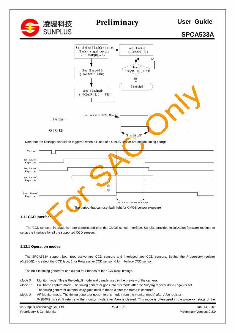
SPCA533A
© Sunplus Technology Co., Ltd.
Proprietary & Confidential
PAGE 108 Jun. 14, 2001
Preliminary Version: 0.2.0
Preliminary User Guide
Set SelectFlashCtr, to let flashcrt signal output(0x201B[0] = 1)
Finished
set flashtrg (0x2A09[4])
Done ?0x2A09[4] ? = 0
Yes
No
Set Flashmode (0x2A09[2:0] = 3'h0)
Set flashwidth (0x2A08, 0x2A07)
Set register 0x2909[4]
flashwidth
Flashtrg
GPIO[12]
Note that the flashlight should be triggered when all lines of a CMOS sensor are accumulating charge.
Vsync
1st Row of Exposure
2st Row of Exposure
3st Row of Exposure
Last Row of Exposure
The interval can use flash light
The period that can use flash light for CMOS sensor exposure
1.11 CCD Interface
The CCD sensors’ interface is more complicated than the CMOS sensor interface. Sunplus provides initialization firmware routines to
setup the interface for all the supported CCD sensors.
1.12.1 Operation modes:
The SPCA533A support both progressive-type CCD sensors and interlaced-type CCD sensors. Setting the Progressen register
(0x2B00[1]) to select the CCD type, 1 for Progressive CCD sensor, 0 for Interlace CCD sensor.
The built-in timing generator can output four modes of the CCD clock timings.
Mode 0: Monitor mode. This is the default mode and usually used in the preview of the camera.
Mode 1: Full frame capture mode. The timing generator goes into this mode after the Snaptrg register (0x2B05[4]) is set.
The timing generator automatically goes back to mode 0 after the frame is captured.
Mode 2: AF Monitor mode. The timing generator goes into this mode (from the monitor mode) after Afen register
0x2B00[2] is set. It returns to the monitor mode after Afen is cleared. This mode is often used in the power-on stage of the
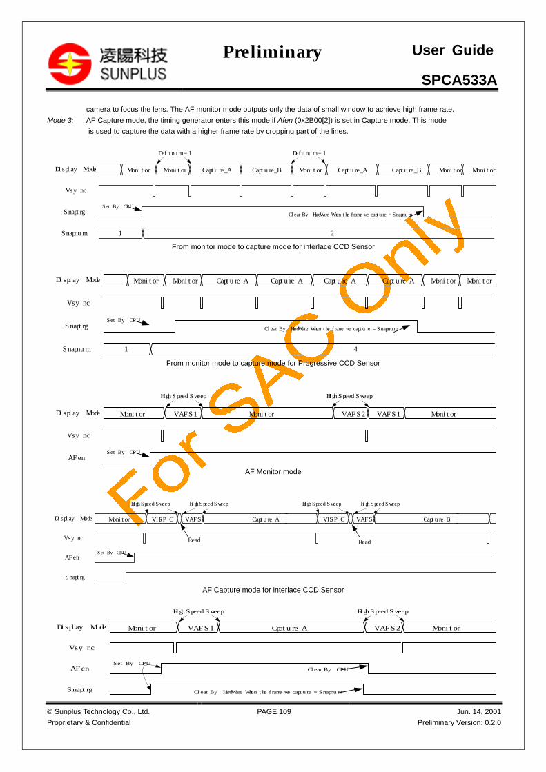
SPCA533A
© Sunplus Technology Co., Ltd.
Proprietary & Confidential
PAGE 109 Jun. 14, 2001
Preliminary Version: 0.2.0
Preliminary User Guide
camera to focus the lens. The AF monitor mode outputs only the data of small window to achieve high frame rate.
Mode 3: AF Capture mode, the timing generator enters this mode if Afen (0x2B00[2]) is set in Capture mode. This mode
is used to capture the data with a higher frame rate by cropping part of the lines.
MonitorMonitor Monitor Monitor MonitorCapture_A Capture_A Capture_BCapture_BDisplay Mode
Vsync
Snaptrg
Snapnum 1 2
Defunum = 1
Set By CPU
Clear By HardWare When the frame we capture = Snapnum
Defunum = 1
From monitor mode to capture mode for interlace CCD Sensor
MonitorMonitor Capture_A Capture_ADisplay Mode
Vsync
Snaptrg
Snapnum 1 4
Set By CPU
Clear By HardWare When the frame we capture = Snapnum
Monitor MonitorCapture_A Capture_A
From monitor mode to capture mode for Progressive CCD Sensor
Monitor MonitorDisplay Mode
Vsync
AFenSet By CPU
VAFS1 VAFS2 MonitorVAFS1
High Speed Sweep High Speed Sweep
AF Monitor mode
Monitor Capture_ADisplay Mode
Vsync
AFenSet By CPU
VHSP_C
High Speed SweepHigh Speed Sweep
VAFS1 Capture_BVHSP_C
High Speed SweepHigh Speed Sweep
VAFS1
Read Read
Snaptrg
AF Capture mode for interlace CCD Sensor
Monitor Cpature_ADisplay Mode
Vsync
AFenSet By CPU
VAFS1 VAFS2Monitor
High Speed Sweep High Speed Sweep
Snaptrg Clear By HardWare When the frame we capture = Snapnum
Clear By CPU

SPCA533A
© Sunplus Technology Co., Ltd.
Proprietary & Confidential
PAGE 110 Jun. 14, 2001
Preliminary Version: 0.2.0
Preliminary User Guide
AF Capture mode for Progressive CCD Sensor
1.12.2 Electronic shutter control
The electronic shutter is used to control the exposure time for the CCD sensors.
MonitorDisplay Mode Capture_A Monitor
Vsync
Sub
EsptimeRead ReadEsptime Esptime
Progressive CCD electronic shutter control
Monitor Capture_ADisplay Mode
Vsync
VHSP_C
High Speed Sweep
Capture_BVHSP_C
High Speed Sweep
Read Read
Monitor
Sub
Esptime Esptime
Mshutter
Interlace CCD electronic shutter control
There are four methods to adjust exposure time in the SPCA533.
1. Adjusting the exposure time based on line:
Set Esptime (0x2B0B, 0A) to determinate the exposure time unit by line.
Hsync
Sub
Esptime EsptimeRead Read
Hsync
Sub
Subfall
Subrise
MonitorDisplay Mode Monitor Monitor
Vsync
The Exposure time control for line base
2. Adjusting the exposure time based on pixel:
Adjust subrise (0x2B24, 23) and subfall (0x2B26, 25) can change the exposure position unit by pixel.
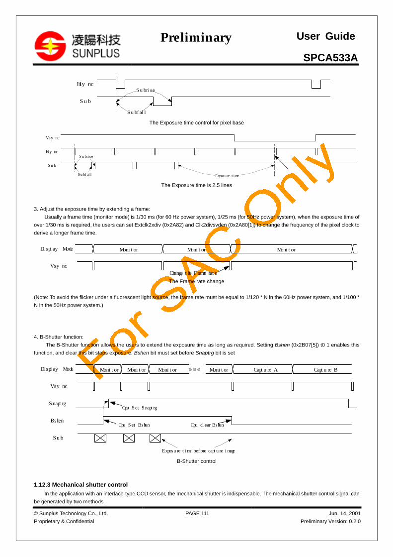
SPCA533A
© Sunplus Technology Co., Ltd.
Proprietary & Confidential
PAGE 111 Jun. 14, 2001
Preliminary Version: 0.2.0
Preliminary User Guide
Hsync
Sub
Subfall
Subrise
The Exposure time control for pixel base
Hsync
Sub
Subfall
Subrise
Vsync
Exposure time
The Exposure time is 2.5 lines
3. Adjust the exposure time by extending a frame:
Usually a frame time (monitor mode) is 1/30 ms (for 60 Hz power system), 1/25 ms (for 50Hz power system), when the exposure time of
over 1/30 ms is required, the users can set Extclk2xdiv (0x2A82) and Clk2divsvden (0x2A80[1]) to change the frequency of the pixel clock to
derive a longer frame time.
MonitorDisplay Mode Monitor Monitor
Vsync
Change the Frame rate
The Frame rate change
(Note: To avoid the flicker under a fluorescent light source, the frame rate must be equal to 1/120 * N in the 60Hz power system, and 1/100 *
N in the 50Hz power system.)
4. B-Shutter function:
The B-Shutter function allows the users to extend the exposure time as long as required. Setting Bshen (0x2B07[5]) t0 1 enables this
function, and clear this bit stops exposure. Bshen bit must set before Snaptrg bit is set
Display Mode
Vsync
MonitorMonitorMonitor Monitor Capture_A Capture_B
Bshen
Sub
Cpu Set Bshen
Exposure time before capture image
Cpu clear Bshen
SnaptrgCpu Set Snaptrg
B-Shutter control
1.12.3 Mechanical shutter control
In the application with an interlace-type CCD sensor, the mechanical shutter is indispensable. The mechanical shutter control signal can
be generated by two methods.
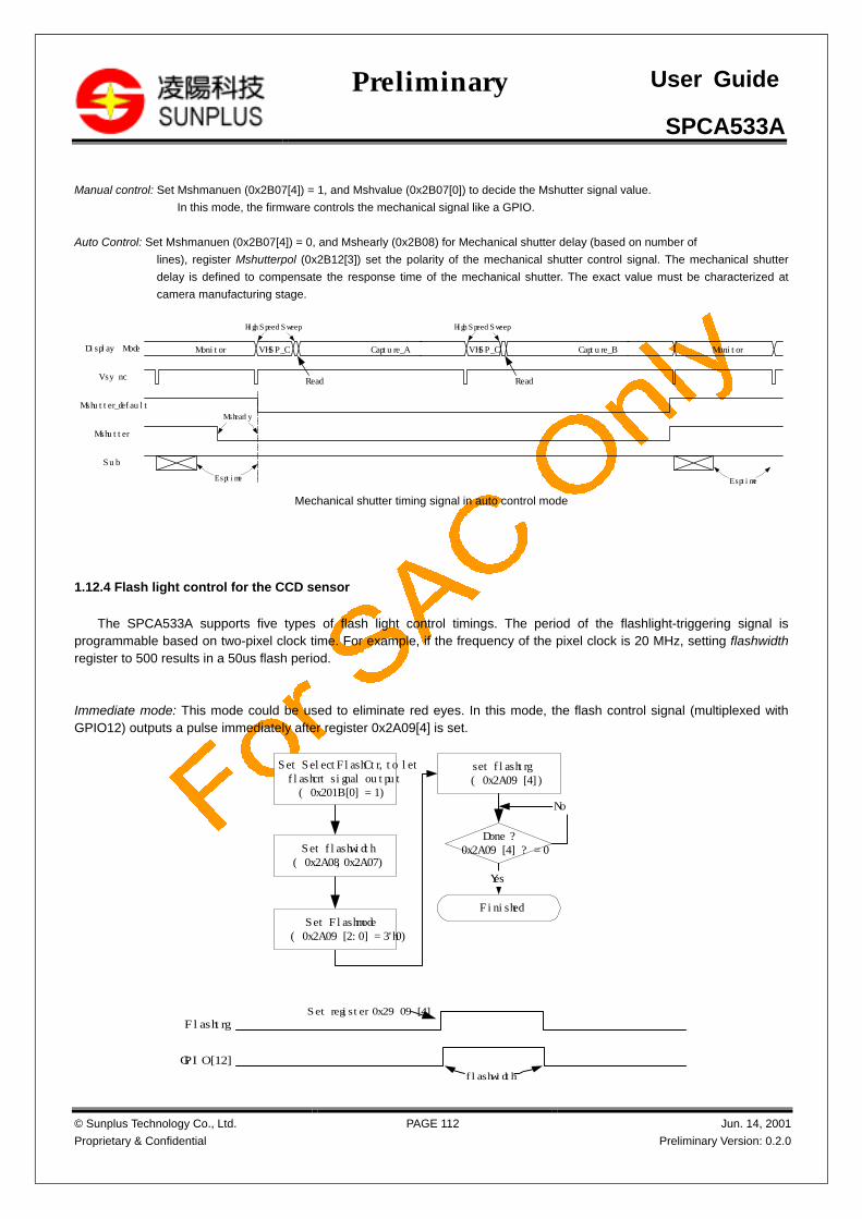
SPCA533A
© Sunplus Technology Co., Ltd.
Proprietary & Confidential
PAGE 112 Jun. 14, 2001
Preliminary Version: 0.2.0
Preliminary User Guide
Manual control: Set Mshmanuen (0x2B07[4]) = 1, and Mshvalue (0x2B07[0]) to decide the Mshutter signal value.
In this mode, the firmware controls the mechanical signal like a GPIO.
Auto Control: Set Mshmanuen (0x2B07[4]) = 0, and Mshearly (0x2B08) for Mechanical shutter delay (based on number of
lines), register Mshutterpol (0x2B12[3]) set the polarity of the mechanical shutter control signal. The mechanical shutter
delay is defined to compensate the response time of the mechanical shutter. The exact value must be characterized at
camera manufacturing stage.
Monitor Capture_ADisplay Mode
Vsync
VHSP_C
High Speed Sweep
Capture_BVHSP_C
High Speed Sweep
Read Read
Monitor
Sub
Esptime Esptime
Mshutter_default
Mshutter
Mshearly
Mechanical shutter timing signal in auto control mode
1.12.4 Flash light control for the CCD sensor
The SPCA533A supports five types of flash light control timings. The period of the flashlight-triggering signal isprogrammable based on two-pixel clock time. For example, if the frequency of the pixel clock is 20 MHz, setting flashwidthregister to 500 results in a 50us flash period.
Immediate mode: This mode could be used to eliminate red eyes. In this mode, the flash control signal (multiplexed withGPIO12) outputs a pulse immediately after register 0x2A09[4] is set.
Set SelectFlashCtr, to let flashcrt signal output(0x201B[0] = 1)
Finished
set flashtrg (0x2A09[4])
Done ?0x2A09[4] ? = 0
Yes
No
Set Flashmode (0x2A09[2:0] = 3'h0)
Set flashwidth (0x2A08, 0x2A07)
Set register 0x2909[4]
flashwidth
Flashtrg
GPIO[12]
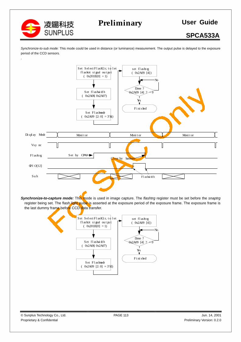
SPCA533A
© Sunplus Technology Co., Ltd.
Proprietary & Confidential
PAGE 113 Jun. 14, 2001
Preliminary Version: 0.2.0
Preliminary User Guide
Synchronize-to-sub mode: This mode could be used in distance (or luminance) measurement. The output pulse is delayed to the exposure
period of the CCD sensors.
.
Set SelectFlashCtr, to let flashcrt signal output(0x201B[0] = 1)
Finished
set flashtrg (0x2A09[4])
Done ?0x2A09[4] ? = 0
Yes
No
Set Flashmode (0x2A09[2:0] = 3'h1)
Set flashwidth (0x2A08, 0x2A07)
Sub
MonitorDisplay Mode Monitor Monitor
Vsync
Flashtrg
GPIO[12]
Set by CPU Clear by hardware
Flashwidth
Synchronize-to-capture mode: This mode is used in image capture. The flashtrg register must be set before the snaptrgregister being set. The flash light pulse is asserted at the exposure period of the exposure frame. The exposure frame isthe last dummy frame before CCD data transfer.
Set SelectFlashCtr, to let flashcrt signal output(0x201B[0] = 1)
Finished
set flashtrg (0x2A09[4])
Done ?0x2A09[4] ? = 0
Yes
No
Set Flashmode (0x2A09[2:0] = 3'h2)
Set flashwidth (0x2A08, 0x2A07)
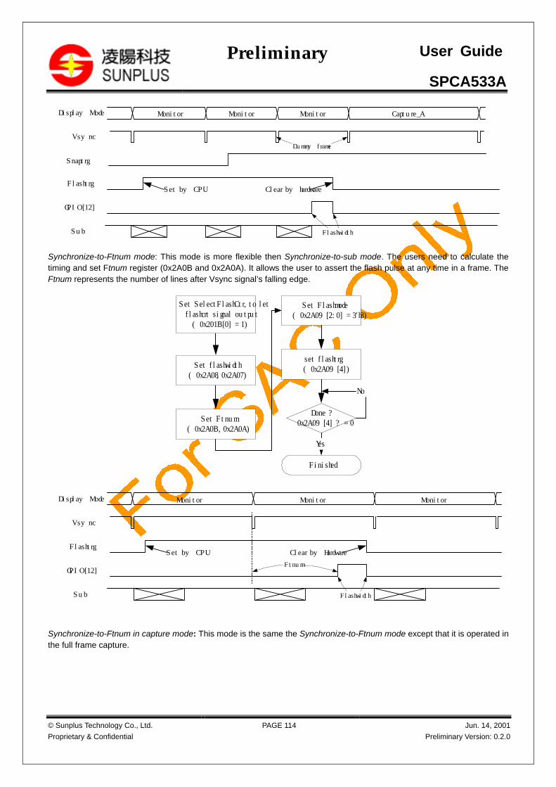
SPCA533A
© Sunplus Technology Co., Ltd.
Proprietary & Confidential
PAGE 114 Jun. 14, 2001
Preliminary Version: 0.2.0
Preliminary User Guide
MonitorDisplay Mode Monitor Monitor
Vsync
Capture_A
Sub
Flashtrg
GPIO[12]
Set by CPU Clear by hardware
Flashwidth
Dummy frame
Snaptrg
Synchronize-to-Ftnum mode: This mode is more flexible then Synchronize-to-sub mode. The users need to calculate thetiming and set Ftnum register (0x2A0B and 0x2A0A). It allows the user to assert the flash pulse at any time in a frame. TheFtnum represents the number of lines after Vsync signal’s falling edge.
Set Ftnum(0x2A0B, 0x2A0A)
Set SelectFlashCtr, to let flashcrt signal output(0x201B[0] = 1)
Finished
set flashtrg (0x2A09[4])
Done ?0x2A09[4] ? = 0
Yes
No
Set flashwidth (0x2A08, 0x2A07)
Set Flashmode (0x2A09[2:0] = 3'h3)
Sub
MonitorDisplay Mode Monitor Monitor
Vsync
Flashtrg
GPIO[12]
Set by CPU Clear by Hardware
Flashwidth
Ftnum
Synchronize-to-Ftnum in capture mode: This mode is the same the Synchronize-to-Ftnum mode except that it is operated inthe full frame capture.

SPCA533A
© Sunplus Technology Co., Ltd.
Proprietary & Confidential
PAGE 115 Jun. 14, 2001
Preliminary Version: 0.2.0
Preliminary User Guide
Set Ftnum(0x2A0B 0x2A0A)
Set SelectFlashCtr, to let flashcrt signal output(0x201B[0] = 1)
Finished
set flashtrg (0x2A09[4])
Done ?0x2A09[4] ? = 0
Yes
No
Set flashwidth (0x2A08, 0x2A07)
Set Flashmode (0x2A09[2:0] = 3'h4)
MonitorDisplay Mode Monitor Monitor
Vsync
Capture_A
Sub
Flashtrg
GPIO[12]
Set by CPU Clear by hardware
Flashwidth
Ftnum
Set by CPU
Dummy frame
Snaptrg

SPCA533A
© Sunplus Technology Co., Ltd.
Proprietary & Confidential
PAGE 116 Jun. 14, 2001
Preliminary Version: 0.2.0
Preliminary User Guide
1.12.5 Image capture
When the SPCA533A is operated with a CCD sensor, the default operating mode of the CCD is monitor mode. The full frame image
capture is started by setting the snaptrg register (0x2B05[4]). The snapnum register (0x2B05[3:0]) defines how many frames are going to be
captured. The Dufenum register (0x2B06[1:0]) defines the number of the dummy frames before capture. Note that the last dummy frame is
the sensors’ exposure frame. The value of the Dufenum register is defined in the CCD sensors’ specification.
Image captures flow
Run Sunplus initial code
Monitor Mode(AFen (0x2B00[2]= 0)
Select operation mode
Capture Image ?
If want ot do Auto focus set AFen to AF Monitor Mode(0x2B00[2]= 1)
No
Yes
Set the number of images to capture (Snapnum 0x2B05[3:0]Set Snaptrg 0x2B05[4]
Done ?(0x2B05[4] ?= 0
Yes
No
Snapnum 4'h1 4'h2
VD MonitorCapture ACapture B MonitorCapture ACapture BMonitorMonitor Monitor MonitorMonitorMonitor
Dummy Frame number = 2 Dummy Frame number = 2
Snaptrg Set By CPUClear By Hardware after the desired number of frames are captured
Field
Image capture for Interlace CCD
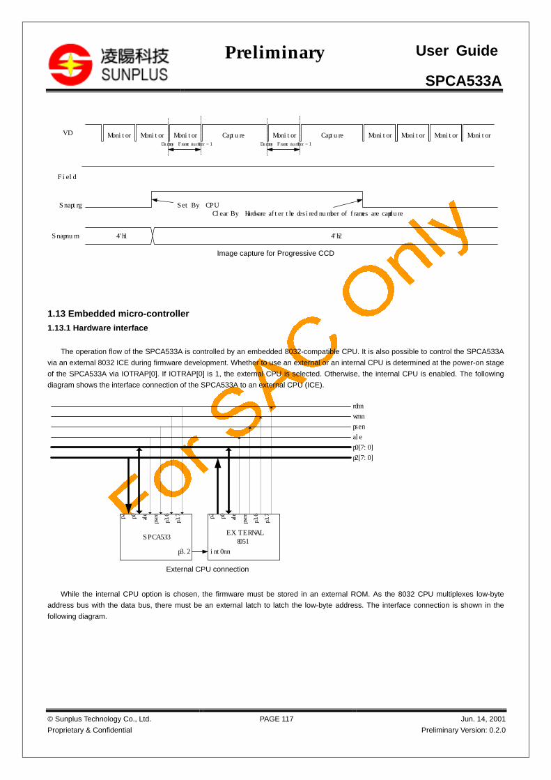
SPCA533A
© Sunplus Technology Co., Ltd.
Proprietary & Confidential
PAGE 117 Jun. 14, 2001
Preliminary Version: 0.2.0
Preliminary User Guide
MonitorVD MonitorMonitorCapture Capture MonitorMonitorMonitorMonitorMonitorDummy Frame number = 1Dummy Frame number = 1
Snapnum 4'h1 4'h2
Snaptrg Set By CPUClear By Hardware after the desired number of frames are captured
Field
Image capture for Progressive CCD
1.13 Embedded micro-controller
1.13.1 Hardware interface
The operation flow of the SPCA533A is controlled by an embedded 8032-compatible CPU. It is also possible to control the SPCA533A
via an external 8032 ICE during firmware development. Whether to use an external or an internal CPU is determined at the power-on stage
of the SPCA533A via IOTRAP[0]. If IOTRAP[0] is 1, the external CPU is selected. Otherwise, the internal CPU is enabled. The following
diagram shows the interface connection of the SPCA533A to an external CPU (ICE).
rdnn
wrnn
psen
ale
p0[7:0]
p2[7:0]
EXTERNAL8051
p2 p0 ale
psen
p3.6
p3.7
SPCA533
int0nnp3.2
p2 p0 ale
psen
p3.6
p3.7
External CPU connection
While the internal CPU option is chosen, the firmware must be stored in an external ROM. As the 8032 CPU multiplexes low-byte
address bus with the data bus, there must be an external latch to latch the low-byte address. The interface connection is shown in the
following diagram.
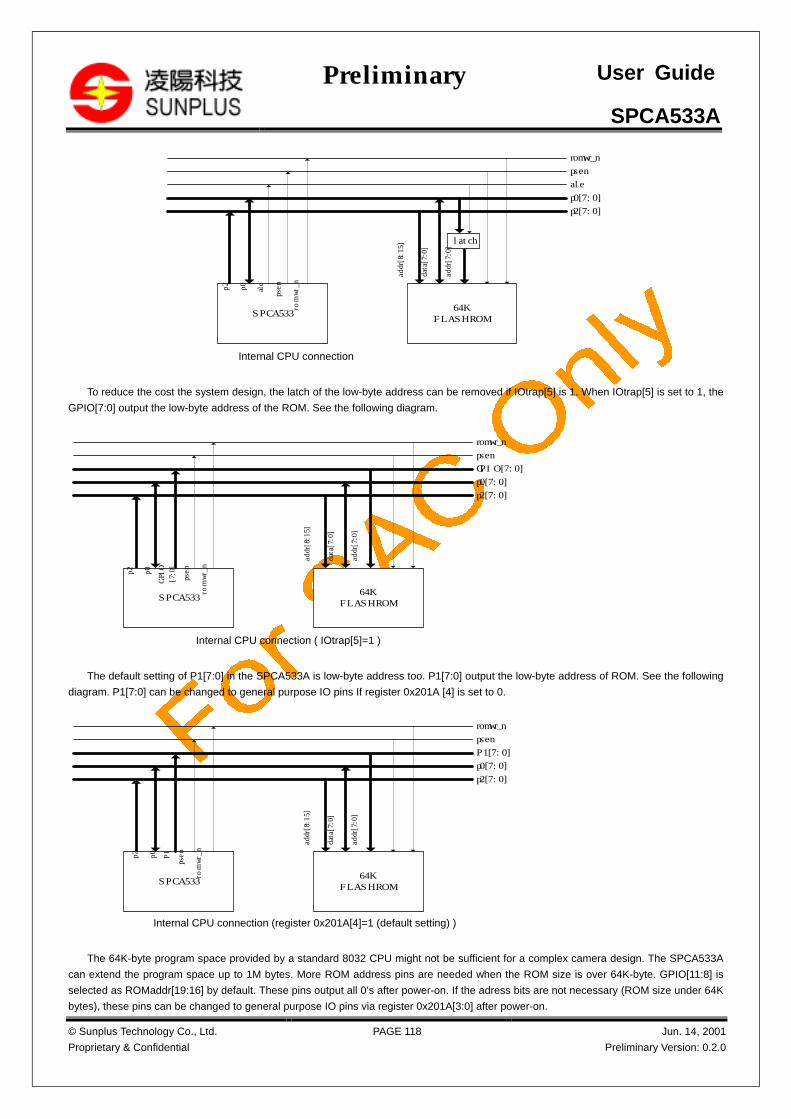
SPCA533A
© Sunplus Technology Co., Ltd.
Proprietary & Confidential
PAGE 118 Jun. 14, 2001
Preliminary Version: 0.2.0
Preliminary User Guide
romwr_n
psen
ale
p0[7:0]
p2[7:0]
SPCA53364K
FLASH ROM
latchp2
p0
ale
psen
romwr_n
addr[8:15]
data[7:0]
addr[7:0]
Internal CPU connection
To reduce the cost the system design, the latch of the low-byte address can be removed if IOtrap[5] is 1. When IOtrap[5] is set to 1, the
GPIO[7:0] output the low-byte address of the ROM. See the following diagram.
romwr_n
psen
GPIO[7:0]
p0[7:0]
p2[7:0]
SPCA53364K
FLASH ROM
p2
p0
GPIO
[7:0]
psen
romwr_n
addr[8:15]
data[7:0]
addr[7:0]
Internal CPU connection ( IOtrap[5]=1 )
The default setting of P1[7:0] in the SPCA533A is low-byte address too. P1[7:0] output the low-byte address of ROM. See the following
diagram. P1[7:0] can be changed to general purpose IO pins If register 0x201A [4] is set to 0.
romwr_n
psen
P1[7:0]
p0[7:0]
p2[7:0]
SPCA53364K
FLASH ROM
p2
p0
P1
psen
romwr_n
addr[8:15]
data[7:0]
addr[7:0]
Internal CPU connection (register 0x201A[4]=1 (default setting) )
The 64K-byte program space provided by a standard 8032 CPU might not be sufficient for a complex camera design. The SPCA533A
can extend the program space up to 1M bytes. More ROM address pins are needed when the ROM size is over 64K-byte. GPIO[11:8] is
selected as ROMaddr[19:16] by default. These pins output all 0’s after power-on. If the adress bits are not necessary (ROM size under 64K
bytes), these pins can be changed to general purpose IO pins via register 0x201A[3:0] after power-on.

SPCA533A
© Sunplus Technology Co., Ltd.
Proprietary & Confidential
PAGE 119 Jun. 14, 2001
Preliminary Version: 0.2.0
Preliminary User Guide
Multi-function pin ‘P3INT’
When IOTRAP[0] = 0, the pin ‘p3int’ is connected to the embedded 8051 P3.3. However, if IOTRAP[0] = 1, the pin ‘p3int’ is connected to the
internal interrupt event. To make ICE function works the same way as embedded 8051, ‘p3int’ have to be connected to external P3.2. The
interface is shown below.
SPCA533
internal8051
interruptsource
p3.2p3.3
p3int
IOTRAP[0] = 0,internal CPU
SPCA533
internal8051
interruptsource
p3.2p3.3
p3int
IOTRAP[0] = 1,external CPU
external8051
p3.2
1.13.2 RAM space
The 8032 CPU can address up to 64K-byte memory. SPCA533A has built-in an 8K-byte SRAM which occupies the lowest 8K-byte
address space. From address 0X2000 to 0X2FFF is 4K-byte space reserved for the camera control. The upper 32K-byte spcae, from
address 0X8000 to 0XFFFF, can be remapped to the ROM space to access ROM data directly. All the unused space can be used by the
external device with additional decoding circuit.
0X0000
0XFFFF
0X20000X2FFF
0X8000
1M ROM
Rampage = 0
Rampage = 1
Rampage= 2
Rampage= 3
Rampage= 31
Internal register
Built-in 8K bytesSRAM
Ram space
32K
address mapping isaccording to Rampage[4:0]
Data Memory
External ROM

SPCA533A
© Sunplus Technology Co., Ltd.
Proprietary & Confidential
PAGE 120 Jun. 14, 2001
Preliminary Version: 0.2.0
Preliminary User Guide
The embedded 8K-byte SRAM is partitioned to low 4K-byte(address 0X0000 ~ 0X0FFF) and high 4K-byte (address 0X1000 ~ 0X1FFF).
Setting register 0X2C00[0] to 1 will enable the low 4K-byte SRAM. Setting register 0X2C00[1] to 1 will enable the high 4K-byte SRAM. While
the low 4K-byet SRAM can only be accessed via the corresponding address space, the high 4K-byte SRAM have three access modes. The
mode register is in register 0X2C11[1:0]. When 0X2C11[1:0] is set to 0, the CPU can access this SRAM via address space 0X1000 to
0X1FFF. When 0X2C11[1:0] is set to 1, the CPU access this SRAM via the data port 0X2C10. The address of SRAM is automatically
incremental by one each time the CPU accessed the data port. This will speed up the firmware execution because the the address
increment is done by hardware. Setting register 0x2C11[2] will reset the address to initial address (register 0x2C12 , 0x2C13). When
0X2C11[1:0] is set to 2, the CPU cannot access the SRAM. The SRAM access right is granted to the DMA controller in this mode. This will
allowed a fast data swap between the high 4K-byte SRAM and other DMA clients. For example, to swap the data between the DRAM and
SRAM. This feature is useful especially when the firmware needs to construct the FAT in the DRAM. The DRAM in an SPCA533-based
application can only be accessed by an indirect addressing method. It is relatively slow comparing with access to the SRAM.
Address 0X8000 to 0XFFFF can be mapped to the ROM space if register 0X2C00[2] is set to 1. This feature allows the CPU to access
the contents of the external ROM via the RAM space. The size of this space is 32K-byte, which corresponds to a ROM bank. Which bank of
the external ROM will be mapped to this RAM space is determined by RAMpage register (SFR 8’h9B). As the SPCA533A support up to
1M-byte ROM space, there are 32 banks to be chosen. In a typical application, the OSD font or some graphic icons are placed in the higher
banks of the external ROM. It is more convenient to access the data via the RAM space. Another application of this feature is when the
firmware needs to be updated. The CPU can write the external ROM (flash-type) via this RAM space. This ISP (In-system-programming)
function will be described more later.
1.13.3 ROM space
The SPCA533A supports 1M-byte physical programming space by bank-switching method. The 1M-byte space is partitioned into 32
banks. The size of each bank is 32K-bytes. The size of the logical space of the 8032 is only 64K-byte. The first bank of the logical
programming space(address 0X0000~X7FFF) is mapped to the physical ROM address 0X0000 to 0X7FFF. The second bank of the logical
programming space can be mapped to any bank of the physical ROM space if register 0X2C00[3] is set to 1. ROMpage (SFR 8’h9A)
determines which bank to be mapped. By using this bank-switching approach, the programming space is extended to 1M-byte. The following
diagram shows the ROM space mapping method.

SPCA533A
© Sunplus Technology Co., Ltd.
Proprietary & Confidential
PAGE 121 Jun. 14, 2001
Preliminary Version: 0.2.0
Preliminary User Guide
Fixed ROM space
0X0000
0XFFFF
Variable ROM space
0X8000
0X7FFF
1M ROM
Rompage= 0
Rompage= 1
Rompage= 2
Rompage = 30
32K
address mapping isaccording to Rompage
address is fixed
program memory
External ROM
Depending on the size of the external ROM, extra address pins should be connected to the external ROM. The extra ROM address pins
are shared multiplexes with the GPIO[11:8]. The function of these pins must be set right after power-on. The SPCA533A assume 1M-byte
external ROM is selected by default. The following table shows the pin configuration for different ROM sizes. The function selection is
controlled by register 0X201A[3:0]
Pin function
ROM size (bytes) GPIO[11] GPIO[10] GPIO[9] GPIO[8]
64K GPIO GPIO GPIO GPIO
128K GPIO GPIO GPIO Romaddr[16]
256K GPIO GPIO Romaddr[17] Romaddr[16]
512K GPIO Romaddr[18] Romaddr[17] Romaddr[16]
1M Romaddr[19] Romaddr[18] Romaddr[17] Romaddr[16]
1.13.4 ISP (In-system-programming)
The In-system-programming is achieved by downloading a new version of firmware and writing it to the external flash-type ROM. The
key concept of the ISP is to shadow the ISP firmware code to the RAM space before updating the ROM. While updating the ROM code, the
CPU execute the program from the SRAM. The shadow space is fixed at 4K. This means the size of the shadow program must be under
4K-byte. Normally the source of the new code is sent by a PC via the USB Bulk pipe, so the ISP firmware code must include the USB-
processing part. The ShadowMap register (0X2C01[7:0]) determined which section of program is to be shadowed. The default is to shadow
the lowest 4K-byte.
The ISP procedures is described below.
1. Moving the ISP section of program to the SRAM (from ROM),
The SRAM shadow space is from address 0x0000 to 0x0fff. So the user must move the code into this region.

SPCA533A
© Sunplus Technology Co., Ltd.
Proprietary & Confidential
PAGE 122 Jun. 14, 2001
Preliminary Version: 0.2.0
Preliminary User Guide
2. Enable shadow function. ( register 0x2C00[4] )
3. Jump to the staring address of the shadow area. Hereafter, the CPU will execute the program from the SRAM, instead of the ROM. The
SPCA533A transforms the ROM read cycle to SRAM read cycle when the access address hit the shadow space and the shadow function is
enabled.
4. The CPU executes the ISP firmware code, which update the external ROM’s contents.
5. Disable shadow function.
The following diagram shows the default mapping of the shadow space.
up to 1M bytes
Program (ROM)space
4K
0X0000
0X0fff
0X0000
Data (SRAM)space
0X0fff
1.13.5 The difference between the standard 8032 and the embedded 8032
The standard 8032 uses open-drained IO buffers. The embedded 8032 CPU does not implement the pull-up mechnism on all CPU-
related pins. To be compatible with the standard 8032, the external pull-up resistors must be connected to P1 and P3[5:0].P0 of the CPU
interface will be driven high (or low) when the CPU needs to output data. P3[6], P3[7] and P2 of the CPU interface is always driven by the
SPCA533A in embedded 8032 operation mode.
For P1 and P3[5:0], the SPCA533A has implemented an alternative approach, which drives P1 and P3[5:0] all the time. The external
pull-up resistors can be spared. This is controlled by register 0X2C02 and 0X2C03. When these registers are set to 1, the corresponding pin
is a general purpose output. To use these pins as general purpose inputs, the corresponding registers must be set to 0 and the
corresponding special function register must be set, too. For example, if P1[7:1] is used for output pins, P1[0] is used input. Fill 0x2C02 as
8’b11111110 and SETB P1.0.
1.13.6 Suspend state power control of CPU
In suspend state, embedded 8032 clock is stopped. Before that, the CPU related pin must be programmed in the appropritae state to
save power. The powerdown bit (register 0x2C05[0]) is used for shutting down the external ROM while suspend asserted. The related
setting and pin state of CPU in suspend mode is described below. Note that ROM low byte address can be driven from GPIO[7:0] or P1[7:0]
and connect with the external ROM by configuration of IOtrap[5] or programming the register 0x201A[4].
Powerdown = 0 (register 0x2C05[0]=0) Powerdown = 1 (register 0x2C05[0]=1)
Ale LOW LOW
Psen HIGH LOW

SPCA533A
© Sunplus Technology Co., Ltd.
Proprietary & Confidential
PAGE 123 Jun. 14, 2001
Preliminary Version: 0.2.0
Preliminary User Guide
Romwr_n HIGH LOW
P3[6] HIGH HIGH
P3[7] HIGH HIGH
P0[7:0] State at suspend signal asserted LOW
P2[7:0] State at suspend signal asserted LOW
P1[7:0] Programmable via (SFR 8’h90, 0x2C02, 0x201A[4]) Programmable via (SFR 8’h90, 0x2C02, 0x201A[4])
P3[5:0] Programmable via (SFR 8’hB0, 0x2C03[5:0]) Programmable via (SFR 8’hB0, 0x2C03[5:0])
Low byte
address[7:0]
State at suspend signal asserted LOW
1.14 TV output interface
The SPCA533A supports a wide range of display devices, inclufing analog TV output, digital TV output, TFT LCD interface and STN
LCD interface. The type of the display devices can be selected by registers 0X2D00. To fit the resolution of the display device the
SPCA533A has built-in the sclaing function in the LCD/TV interface controller. The firmware of the SPCA533A is obligated to change scaling
factors whenever the display device changes.
While connecting to GRAINTPLUS STN-LCD or PRIME VIEW TFT LCD , the tvenc1xck clock must be chage to 27MHz (register 0X201C).
It is different from another interface.
1.14.1 Analog TV interface (tvdspmode=0~1, register 0X2D00)
The built-in TV encoder of the SPCA533A can generate standard NTSC and PAL compositive video signals. The SPCA533A has also buitl-
in a video DAC for the TV signal output. During operation, the DAC consumes about 30mA current. It is important to turn off the DAC while it
is not in operation. The DAC can be turned on by setting register 0X2001.The application circuit of the DAC interface is shown below.
SPCA533
VREF
COUT
RSET
CBL
CBU
1.4K
75
0.1uF
0.1uF
VDDA
1.14.2 Digital TV interface
In this chapter, we discuss the digital TV interface including the CCIR601, CCIR656, UPS051, STN-LCD, CASIO, VGA TFT-LCD
and EPSON interface.
5.14.2.1 CCIR 656 interface (dspmode=2~3, register 0X2D00)
The CCIR656 digital video protocol does not transmit the whole horizontal blanking interval. Instead, it inserts a special four-word codes into
the digital video stream to indicate the start of active video (SAV) and end of active video (EAV). These EAV and SAV codes indicate when
horizontal and vertical blanking are present and which field is being transmitted, enabling most of the horizontal blanking interval to be used
to transmit ancillary data such as line numbering, digital audio data, error checking data, and so on. When this mode is selected, the
SPCA533A encodes the video stream by inserting SAV and EAV code to the video data stream, no ancillary data is encoded. The data bus
is 8-bit wide.

SPCA533A
© Sunplus Technology Co., Ltd.
Proprietary & Confidential
PAGE 124 Jun. 14, 2001
Preliminary Version: 0.2.0
Preliminary User Guide
5.14.2.2 CCIR 601 interface (tvdspmode=4~7, register 0X2D00)
In this display mode, a 16-bit data bus is used. Digtv[7:0] transmits the luminance data and Digtv[15:8] transmits the chrominance data.
RGB2YCbCr matrix:
Y = (77/256)R + (150/256)G + (29/256)B
Cb = -(44/256)R -(87/256)G +(131/256)B + 128
Cr = (131/256)R - (110/256)G - (21/256)B + 128
YCbCr2YUV matrix:
Y = (1/2)(Y-16) + (1/8)(Y-16)
U = (1/2)(Cb-128) + (1/32)(Cb-128)
V = (1/2)(Cr-128) + (1/4)(Cr-128)
1.14.2.3 Unipac UPS051 (TFT-LCD interface, dspmode=8, register 0X2D00)
SPCA533A can interface to the Unipac’s UPS051 LCD controller, which in turns, drives Unipac’s TFT LCD panel. The following diagram
shows the interface timing.
R0 R1 R2 R3 R4 R5 R6 R7 R8 R9 R10 R11 R12 R13 R14 R15
B0 B1 B2 B3 B4 B5 B6 B7 B8 B9 B10 B11 B12 B13 B14 B15
G0 G1 G2 G3 G4 G5 G6 G7 G8 G9 G10 G11 R12 G13 G14 G15
HS
VCLK
Rn
Gn
Bn
DCLK
G8 B10B3G1 R6 R13 G15even lineDn
R8 G10G3R1 B6 B13 R15odd line Dn
1.14.2.4 EPSON D-TFD LCD interface (tvdspmode=10, register 0X2D00)
SPAC533 had build in em1812b for control of the D-TFD liquid crystal panel module LF18DB series. The D-TFD liquid crystal panel block
uses active matrix panel. By the way, SPCA533A need extera control circuit for driving the panel module. And SPCA533A is not equipped
with an inverter for driving the backlight module. Register 0X2D02~0X2D0F must be redefined reference as section 5.14.2.8. The resolution
of EPSON LCD panel is 312 (horizontal) X 230 (vertical) dots.
1.14.2.5 CASIO TFD LCD interface (tvdspmode=11, register 0X2D00)
The driving timing has 263 lines per frame and 858 pixel per line. To prevent display retention, please set up stand-by mode or cut off the
power after writing white display data at least 2 field. (Register 0X2D25, bit 4) After power-on, the GRES must be kept low for at least 2 field
periods while sending normal signals to the other inputs. (Register 0X2D25, bit 5)
1.14.2.6 GIANTPLUS STN-LCD interface (tvdspmode=12, register 0X2D00)
SPCA533A support multiple resolution STN-LCD panel including 320x240, 240x160 and 160x120. In other words, register
0X2B02~0X2B0F must be programmable. The timing diagram of STN-LCD had shown in below. However, its frame rate depends on the
register setting. You can insert a few pixels in vsync or hsync interval to reduce the panel frame rate.
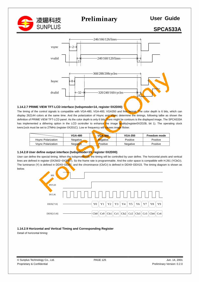
SPCA533A
© Sunplus Technology Co., Ltd.
Proprietary & Confidential
PAGE 125 Jun. 14, 2001
Preliminary Version: 0.2.0
Preliminary User Guide
vsync
vvalid 240/160/120/lines
246/166/126/lines
2
2 2
hsync
dvalid 320/240/160/cycles
368/288/208cycles
8
328
1.14.2.7 PRIME VIEW TFT-LCD interface (tvdspmode=14, register 0X2D00)
The timing of the control signals is compatible with VGA-480, VGA-400, VGA350 and free format. The color depth is 6 bits, which can
display 262144 colors at the same time. And the polarization of Hsync and Vsync determine the timings, following talbe as shown the
definition of PRIME VIEW TFT-LCD panel. As the color depth is only 6 bits, there might be contours is the displayed image. The SPCA533A
has implemented a dithering option in the LCD ocntroller to enhance the image quality(register0X2D2B, bit 1). The operating clock
tvenc1xck must be set to 27MHz (register 0X201C). Low er frequency will causes image flicker.
VGA-480 VGA-400 VGA-350 Freedom mode
Hsync Polarization Negative Negative Positive Positive
Vsync Polarization Negative Positive Negative Positive
1.14.2.8 User define output interface (tvdspmode=15, register 0X2D00)
User can define the special timing. When the tvdspmode=15, the timing will be controlled by user define. The horizontal pixels and vertical
lines are defined in register (0X2b02~0X2B07). So the frame rate is programmable. And the color space is compatible with H.261 (YCbCr).
The luminance (Y) is defined in DDX0~DDX7, and the chrominance (Cb/Cr) is defined in DDX8~DDX15. The timing diagram is shown as
below.
Y0
DCLK
DDX[7:0]
DDX[15:8]
Y1 Y2 Y3 Y4 Y5 Y6 Y7
Cb0 Cr0 Cb1 Cr1 Cb2 Cr2 Cb3 Cr3
HVLD
HS
Y8 Y9
Cb4 Cr4
1.14.2.9 Horizontal and Vertical Timing and Corresponding Register
Detail of horizontal timing:

SPCA533A
© Sunplus Technology Co., Ltd.
Proprietary & Confidential
PAGE 126 Jun. 14, 2001
Preliminary Version: 0.2.0
Preliminary User Guide
A B C D
E
mode Item Description Clock Cycles Time register
A Horizontal Width 63 4.66 µs hsyncw=63(default)
B Horizontal B-porch 65 4.81 µs vldx0=128
C Horizontal Display 720 53.28 µs vldx1=847
D Horizontal F-porch 10 0.75 µs
NTSC
(analog &
CCIR)
E Horizontal Total 858 63.5 µs hpixel=857(default)
A Horizontal Width 64 4.7 µs hsyncw=64(default)
B Horizontal B-porch 64 4.7 µs vldx0=128
C Horizontal Display 720 53.28 µs vldx1=847
D Horizontal F-porch 16 1.32 µs
PAL
(analog &
CCIR)
E Horizontal Total 864 64 µs hpixel=863(default)
A Horizontal Width 98 7.26 µs hsyncw=98
B Horizontal B-porch 36 2.67 µs vldx0=134
C Horizontal Display 689 51.04 µs vldx1=822
D Horizontal F-porch 35 2.53 µs
UNIPAC
E Horizontal Total 858 63.5 µs hpixel=857
A Horizontal Width 32 2.37 µs hsyncw=32
B Horizontal B-porch 52 3.85 µs vldx0=84
C Horizontal Display 624 46.22 µs vldx1=708
D Horizontal F-porch 202 14.96 µs
EPSON
E Horizontal Total 910 67.4 µs hpixel=909
A Horizontal Width 4 0.3 µs hsyncw=4
B Horizontal B-porch 18 1.33 µs vldx0=20
C Horizontal Display 708 52.44 µs vldx1=728
D Horizontal F-porch 128 9.43 µs
CASIO
E Horizontal Total 858 63.5 µs hpixel=857
A Horizontal Width 8 0.3µs hsyncw=8
B Horizontal B-porch 32 1.18 µs vldx0=40
C Horizontal Display 320 11.85 µs vldx1=359
D Horizontal F-porch 8 0.3 µs
STN-LCD
320x240
E Horizontal Total 368 13.63 µs hpixel=367
A Horizontal Width 8 0.3µs hsyncw=8
B Horizontal B-porch 32 1.18 µs vldx0=40
C Horizontal Display 240 8.89µs vldx1=279
D Horizontal F-porch 8 0.3 µs
STN-LCD
240x160
E Horizontal Total 288 10.67 µs hpixel=287
A Horizontal Width 8 0.3µs hsyncw=8
B Horizontal B-porch 32 1.18 µs vldx0=40
C Horizontal Display 160 5.92 µs vldx1=199
D Horizontal F-porch 8 0.3 µs
STN-LCD
160x120
E Horizontal Total 208 7.7 µs hpixel=207
VGA-480
VGA-400
VGA-350
A Horizontal Width 96 3.813 µs hsyncw=96

SPCA533A
© Sunplus Technology Co., Ltd.
Proprietary & Confidential
PAGE 127 Jun. 14, 2001
Preliminary Version: 0.2.0
Preliminary User Guide
B Horizontal B-porch 48 1.907 µs vldx0=144
C Horizontal Display 640 25.422 µs vldx1=783
D Horizontal F-porch 16 0.636 µs
E Horizontal Total 800 31.778 µs hpixel=799
Detail of vertical timing:
A B C D
E
mode Item Description Horizontal Lines Time register
A Vertical Width 3 190.5 µs vsyncw (default)
B Vertical B-porch 16 1.02 ms vldy0=16
C Vertical Display 240 15.24 ms vldy1=255
D Vertical F-porch 3.5 219.5 µs
NTSC
(analog&
CCIR)
E Vertical Total 262.5 16.67 ms vline (default)
A Vertical Width 3 192 µs vsyncw (default)
B Vertical B-porch 19 1.22 ms vldy0=19
C Vertical Display 288 18.43 ms vldy1=306
D Vertical F-porch 2.5 158 µs
PAL (analog&
CCIR)
E Vertical Total 312.5 20 ms vline (default)
A Vertical Width 3 190.5 µs vsyncw=3
B Vertical B-porch 25 1.59 ms vldy0=25
C Vertical Display 220 13.97 ms vldy1=244
D Vertical F-porch 14 849.5 µs
UNIPAC
E Vertical Total 262 16.6 ms vline=261
A Vertical Width 4 269.6 µs vsyncw=4
B Vertical B-porch 19 1.28 ms vldy0=19
C Vertical Display 230 15.5 ms vldy1=248
D Vertical F-porch 9 610.4 µs
EPSON
E Vertical Total 262 17.66 ms vline=261
A Vertical Width 3 190.5 µs vsyncw=3
B Vertical B-porch 16 1.02 ms vldy0=16
C Vertical Display 240 15.24 ms vldy1=255
D Vertical F-porch 3.5 219.5 µs
CASIO
E Vertical Total 262.5 16.67 ms vline=262
A Vertical Width 2 27.26 µs vsyncw=2
B Vertical B-porch 2 27.26 µs vldy0=2
C Vertical Display 240 3.27 ms vldy1=241
D Vertical F-porch 2 27.26 µs
STN-LCD
320x240
E Vertical Total 246 3.35 ms vline=245
A Vertical Width 2 21.34 µs vsyncw=2
B Vertical B-porch 2 21.34 µs vldy0=2
C Vertical Display 160 1.71 ms vldy1=161
D Vertical F-porch 2 21.34 µs
STN-LCD
240x160
E Vertical Total 166 1.77 ms vline=165

SPCA533A
© Sunplus Technology Co., Ltd.
Proprietary & Confidential
PAGE 128 Jun. 14, 2001
Preliminary Version: 0.2.0
Preliminary User Guide
A Vertical Width 2 15.4 µs vsyncw=2
B Vertical B-porch 2 15.4 µs vldy0=2
C Vertical Display 120 924 µs vldy1=121
D Vertical F-porch 2 15.4 µs
STN-LCD
160x120
E Vertical Total 126 970 µs vline=125
A Vertical Width 2 63.5 µs vsyncw=2
B Vertical B-porch 33 1.049 ms vldy0=35
C Vertical Display 480 15.253 ms vldy1=514
D Vertical F-porch 10 317.8 µs
VGA-480
E Vertical Total 525 16.683 ms vline=524
A Vertical Width 2 63.5 µs vsyncw=2
B Vertical B-porch 35 1.112 ms vldy0=37
C Vertical Display 400 12.711 ms vldy1=436
D Vertical F-porch 12 381.0 µs
VGA-400
E Vertical Total 449 14.268 ms vline=448
A Vertical Width 2 63.5 µs vsyncw=2
B Vertical B-porch 60 1.907 ms vldy0=62
C Vertical Display 350 11.122 ms vldy1=411
D Vertical F-porch 37 1.176 ms
VGA-350
E Vertical Total 449 14.268 ms vline=448
image size in DRAMimgvofst[11:0]
imghofst[11:0]
(selwx0,selwy0)
(selwx1,selwy1)
osdvofst
osdhofst
vldx0 vldx1hsyncw ���������������������������������������������������������������������������������������������������������������������������������������������������������������������������������������������������������������������������������������������������������������������������������������������������������������������������������������valid
hpixel
vsyncw
vldy0
vldy1
����������������������������������������������������������������������������������������������������������������
valid
vlin
e
A field/frame timing and corresponding register diagram
1.14.3 On Screen Display (OSD)The SPCA533A supports two types of OSD functions. The first one is font-based OSD, the other one is graphic- based OSD. The font-based
OSD is based on the fixed pitched (15x32) fonts. The advantage of the font-based OSD is smaller storage size requirement. And it is fast to

SPCA533A
© Sunplus Technology Co., Ltd.
Proprietary & Confidential
PAGE 129 Jun. 14, 2001
Preliminary Version: 0.2.0
Preliminary User Guide
operate when the OSD changes. The graphic-based OSD allows the users to deisgn colorful icons with 16-bit color depth. It consumes more
storage space.
1.14.3.1 Font-Based OSD
The font-based OSD function of the SPCA533A allows the users to define 512 fonts in the SDRAM. Each font is defined by 16x32 pixel array;
each pixel is represented by two bits. The OSD font data base occupies 64K bytes SDRAM space in total. Register 0X2759~0x275B defines
the starting address of the OSD data base in the SDRAM.
Just how many pixels on the display device will be mapped by an OSD pixel depends on the resolution of the display device. According to
the register 0X2D21 definition, you can program how many pixels on display device. In TV or larger LCD panel, you can change the register
(0X2D21) to 0X20(default 0X40), so display size will be mapped to 32x32 pixel array.
The display space is partitioned into blocks of 25 columns by 7 rows. Normally, the display devices cannot display so many rows at the same
time due to the resolution. However, it is easier to use the extra rows to prepare the OSD data for the display especially when the application
is to implement a menu-scrolling function. Each partitioned block is assigned by a font index and a display attribute. The font index is 9-bit
long, allowing the controller to index to one of the selected 512 fonts. The display attribute determines the color and other special effects
while rendering the OSD pattern.
The color palette of the SPCA533A defines 9 colors. Eight of them are used in the pattern display (foreground color); the remaining one is
used for background color. Each color is defined by 15-bit registers. The user may define 32768 colors in total. However, only 8 foreground
colors and one background color can be shown on the display device at the same time.
Bit [2:0] of the display attribute buffer defines the (foreground) color. Bit [3] determines whether to turn on the background color. Bit [5:4]
specifies the special display effects, including normal, half tone, foreground/background color exchange and blanking. In other words, the
background color control is independence to special display effect. By the way, font index and color attribute mapping is one-by-one. Every
display block region in SPCA533A has own attribute. The following diagram has shown as the display attribute buffer.
OSDstart
8
SR
AM
25
6X
9
block 253
block 254
block 255
SR
AM
12
8X
4
block 0
block 1
block 2
block 3
.....
.....
.....
font indexcolor index
128bytes
color 0
color 1
color 2
color 3
color 4
color 5
color 6
color 7
color bg
color palette(defined in registers)
32768 colors can be defined8 colors can be shownsimultaneously
index buffer 256X9 bits (25X10=250)color buffer 256X6 bits
osdsfunc[1:0]0: normal display1: show background color/image in half-tone2: reverse background color and solid color3: blinking (based on vsync)
SDRAM space
lan
gu
ag
e s
pe
cifi
c f
ron
t p
ag
ec
om
mo
n f
ron
t p
ag
e
64
K b
yte
sR[4:0] G[4:0] B[4:0]
R[4:0] G[4:0] B[4:0]
R[4:0] G[4:0] B[4:0]
R[4:0] G[4:0] B[4:0]
R[4:0] G[4:0] B[4:0]
R[4:0] G[4:0] B[4:0]
R[4:0] G[4:0] B[4:0]
R[4:0] G[4:0] B[4:0]
R[4:0] G[4:0] B[4:0]
7 6 5 4 3 2 1 005 4 3 2 1
special function bits
block 4
block 5
front 0
front 1
front 2
front 3
.....
front 254
front 255
front 256
front 257
front 510
front 511
.....
.....
.....
.....
.....

SPCA533A
© Sunplus Technology Co., Ltd.
Proprietary & Confidential
PAGE 130 Jun. 14, 2001
Preliminary Version: 0.2.0
Preliminary User Guide
Each font is defined by 16X32 bitmap array
0
osdscrll[2:0]
The LCD screen is partitioned into 25x7 blocks.Each block is linked to a font by an index
25 columns
actual display buffer
1 2 3 4 5 6 7 8 9 10 11 12 13 14 15 16 17 18 19 20 21 22 23 24
25 26 27 28 29 30 31 32 33 34 35 36 37 38 39 40 41 42 43 44 45 46 47 48 49
50
75
In font-based OSD, each pixel is defined by 2 bits.
0: empty (show background color or image)
1: black
2: foreground color blended with image or background color
3: foreground color
To avoid false color, the font-based OSD defines the blending level between forground color and image (or blending with background color).
Register 0X2D52 define the blending level. Furthermore, the TV/LCD interface controoler has built in a low-pass filter to avoid the false
color. Set the register 0X2D2B bit 1 to turn on the filter. The OSD also defines a select window function, which display a highlighted frame.
The size and position of the frame are programmable via register (0X2D10~0X2D18). The following picture demonstrates the special display
effects defined by the attributes.
ROW Attibute[5:3] Effect
1 0 Normal mode and background color disable.
2 1 Normal mode and background color enable. (background color set to blue)
3,4 2 Half-tone mode
5 4 Exchange foreground/background color and background color disable.
6 5 Exchange foreground/background color and background color enable.
7 6 Blinking mode and background color disable.

SPCA533A
© Sunplus Technology Co., Ltd.
Proprietary & Confidential
PAGE 131 Jun. 14, 2001
Preliminary Version: 0.2.0
Preliminary User Guide
1.14.3.2 graphic-based OSD
The graphic-based OSD utilizes the copy&paste engine (in the DRAM controller) to paste the graphic icons to the display buffer. As
the graphic icons are prepared in advance, any image is possible to be used in the graphic OSD. In a practical application, the database of
the graphic-based OSD must be compressed to a JPEG VLC data stream to reduce the size. This database is uploading from the external
ROM to the SDRAM and decompressed at the initialization stage of the SPCA533. The quatization factor in the JPEG compression should
be set to all 1’s to maintain the quality. In the playback mode, pasting a graphic icon to the decompressed image buffer may destroy the
image. It is up to the firmware to backup the original image for image restore later. In the preview mode, it is possible to paste the graphic
OSD to the four side of the image buffer. The CDSP may skip these regions when the incoming image is to be filled into the frame buffer. The
following diagram shows the frame buffer allocation while using the graphic-based OSD in the preview mode.
SENSOR CDSP
define menu bar0X27E7 menuen0X27E8~9 menuhoff0X27EA~B menuvoff0X27EC~D menuhsize0X27EE~F menuvsize
DRAMA/B
BufferTVENC
writeor
skip
The SPCA533A has also implemented the color key function to make the graphic-based OSD more flexible. A color key is defined as
the luminance lower than a pre-defined threshold. It means a black color is the pre-defined color key. The threshold is designed to
compensate image distortion in the JPEG compression/decompression. When the color key function is turned-on, the pixels with the key
color (normally black) will be replaced by the foreground color assigned to the corresponding blocks. Note that even in the graphic systems,
the foreground color is still defined block by block. And the block definition is the same as the one used in the font-based OSD. As
SPCA533A treats the graphic OSD data as image, it is possible to show the graphic-based OSD and font-based OSD at the same time. The
font-based OSD will overlap with the graphic icons when it exists. If the user is to show a pure graphic icon, the font indices on the
corresponding blocks must link to a space (empty) font.
The following diagram depicts the constructing sequence of the image and the OSD. The image or graphic OSD data, which
received from DRAM, will through the color key controller. When the color key function turns on, the luminance lower than the color key
definition will replace by the background color. The background color information is getting from color attribute definition in display buffer. So
the image data will mix with the font definition data by mixer. The mixer controller’s effect was defined by the 2-bit font pixel array. And then,
the register 0X2D30 bit 0 control the real display data whether the mixer data or the background color.
image/Graphic OSD
color keydefinition
backgroundcolor
blendingMixer
0:image 1:black 2:blending 3:FG color
MUXbackground
colorscreen
controller
FontOSD
fontdefine
color map
To TV encoderor controller
1.14.4 Gamma correction
The data output of TV/LCD interface can be remapped by a programmable gamma curve. The curve is constructed by The range of the
input data is from 0 to 255, which is partitioned evenly into 16 section. Each section corresponds to a point. The X-coordinates of these
points are fixed, and the Y coordinates are programmable. The output value is calculated by linear interpolation.
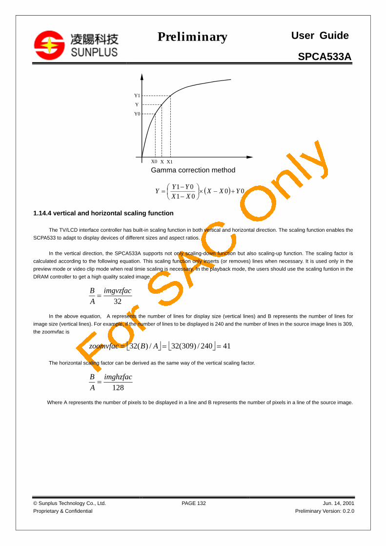
SPCA533A
© Sunplus Technology Co., Ltd.
Proprietary & Confidential
PAGE 132 Jun. 14, 2001
Preliminary Version: 0.2.0
Preliminary User Guide
X0 X1
Y0
Y1
X
Y
Gamma correction method
( ) 0001
01YXX
XX
YYY +−×
−−
=
1.14.4 vertical and horizontal scaling function
The TV/LCD interface controller has built-in scaling function in both vertical and horizontal direction. The scaling function enables the
SCPA533 to adapt to display devices of different sizes and aspect ratios.
In the vertical direction, the SPCA533A supports not only scaling-down function but also scaling-up function. The scaling factor is
calculated according to the following equation. This scaling function only inserts (or removes) lines when necessary. It is used only in the
preview mode or video clip mode when real timie scaling is necessary. In the playback mode, the users should use the scaling funtion in the
DRAM controller to get a high quality scaled image.
32
imgvzfac
A
B=
In the above equation, A represents the number of lines for display size (vertical lines) and B represents the number of lines for
image size (vertical lines). For example, if the number of lines to be displayed is 240 and the number of lines in the source image lines is 309,
the zoomvfac is
41240/)309(32/)(32 === ABzoomvfac
The horizontal scaling factor can be derived as the same way of the vertical scaling factor.
128
imghzfac
A
B=
Where A represents the number of pixels to be displayed in a line and B represents the number of pixels in a line of the source image.

SPCA533A
© Sunplus Technology Co., Ltd.
Proprietary & Confidential
PAGE 133 Jun. 14, 2001
Preliminary Version: 0.2.0
Preliminary User Guide
2. Register Descriptions
2.1 Register Category
Address Description
0X2000 ~ 0X20ff Global Registers
0X2100 ~ 0X21ff CDSP Registers
0X2200 ~ 0X22ff CDSP Window Registers
0X2300 ~ 0X23ff DMA Control Registers
0X2400 ~ 0X24ff Storage Media Control Registers
0X2500 ~ 0X25ff USB Control Registers
0X2600 ~ 0X26ff Audio Control Registers
0X2700 ~ 0X27ff SDRAM Control Registers
0X2800 ~ 0X28ff JPEG Control Registers
0X2900 ~ 0X29ff Synchronous Serial Interface Registers
0X2a00 ~ 0X2aff CMOS Sensor Control Registers
0X2b00 ~ 0X2bff CCD Control Registers
0X2c00 ~ 0X2cff CPU Interface Registers
0X2d00 ~ 0X2dff TV Encode Control Registers
2.2 Global Registers
address bit attar Name Description Default
value
0X2000 2:0 rw Cammode[2:0] Camera operation mode
0: camera idle
1: Preview
2: Digital Still camera mode
3: Video clip mode
4: PC-camera mode
5: Playback mode
6: Upload/Download mode
others: reserved
3’h0
0X2001 0 rw TVEn TV encoder enable bit
0: disable the embedded TV encoder
1: enable the embedded TV encoder
1’b0
1 rw DACTest Embedded DAC test mode
0: normal operation
1: force the DAC into test mode
1’b0
2 rw DACPd Embedded DAC power-down mode
0: normal operation
1:force DAC into power-down mode
1’b1
3 rw DACBGpd DAC reference voltage selection
0: internal
1: external
1’b1
0X2002 0 rw SWTCRst Software reset to Timing generator and CMOS interface
0: normal operation
1:S/W reset
1’b0
1 rw SWCDSPRst Software reset to Color processing engine
0: normal operation
1: S/W reset
1’b0
2 rw SWTVRst Software reset to Color processing engine
0: normal operation
1’b0
SPCA533A
© Sunplus Technology Co., Ltd.
Proprietary & Confidential
PAGE 134 Jun. 14, 2001
Preliminary Version: 0.2.0
Preliminary User Guide
1: S/W reset
3 rw SWUSBRst Software reset to USB controller
0: normal operation
1: S/W reset
1’b0
4 rw SWDRAMPRst Software reset to DRAM controller engine
0: normal operation
1: S/W reset
1’b0
5 rw SWJPEGRst Software reset to JPEG compression engine
0: normal operation
1: S/W reset
1’b0
6 rw SWFMRst Software reset to storage media interface
0: normal operation
1: S/W reset
1’b0
7 rw SWAUDRst Software reset to audio interface
0: normal operation
1: S/W reset
1’b0
0X2003 0 rw SwSuspend Software suspend bit.
0: Normal operation
1: force the chip into suspend state. When this bit is set to 1, Both
the crystal pads oscillation will be stopped.
1’b0
1 rw RSMRstEn Embedded CPU resume reset enable bit.
0: Normal
1: After the camera chip is returned to normal operation state from
the suspend state, the embedded CPU is automatically reset.
1’b0
0X2004 2:0 rw TResume Resume length selection
0: 1ms
1: 2ms
2: 3 ms
3: 5 ms
4: 7 ms
5: 10 ms
6: 15 ms
7: reserved
The embedded PLL needs a period of time to become stable after
the chip returns to the normal operation state from suspend state.
The Tresume register determines how long should the camera wait
until it resume all the clock sources to the internal modules. In
normal cases, 10ms is enough.
2’h0
0X2005 0 rw IntTrxEn Internal USB transceiver enable.
0: disable the internal USB transceiver
1:enable the internal USB transceiver
When the camera is operated off-line (disconnected from the PC),
this bit must be cleared to 0 to conserve power.
1’b1
0x2006 0 rw SWDRAMOe DRAM signal output enable control bits.
0: All DRAM pins are tri-stated.
1: for DRAM normal operation.
1’b0
0X2007 7:0 rw SWTGOe[7:0] TG control signal output enable register.
0: output disabled
1: enable output
[0]: control v1
[1]: control v2
[2]: control v3
[3]: control v4
8’h0

SPCA533A
© Sunplus Technology Co., Ltd.
Proprietary & Confidential
PAGE 135 Jun. 14, 2001
Preliminary Version: 0.2.0
Preliminary User Guide
[4]: control sg1a
[5]: control sg3a
[6]: control sg1b
[7]: control sg3b
0X2008 7:0 rw SWTGOe[15:8] [8]: control sub
[9]: control fr
[10]: control fh1
[11]: control fh2
[12]: control mshutter
[13]: control vsubctrl
[14]: control pblk
[15]: control fs
8’h0
0X2009 3:0 rw SWTGOe[19:16] [16]: control fcds
[17]: control adclp
[18]: control obclp
[19]: control adck
4’b0
0X200a 7:0 rw SWTGIg[7:0] TG control signal input
0: Disable gated to zero.
1: Enable gated to zero.
[0]: control v1
[1]: control v2
[2]: control v3
[3]: control v4
[4]: control sg1a
[5]: control sg3a
[6]: control sg1b
[7]: control adclp
8’hff
0X200b 2:0 rw SWTGIg[9:8] TG control signal input gated to zero register.
[8]: control adck
[9]: control sd
2’h3
0X2010 7:0 rw Clk48mEn The 48MHz Clock
0: disable
1: enable
[0]: CDSP module
[1]: DMA module
[2]: FM module
[3]: USB module
[4]: Audio module
[5]: SDRAM module
[6]: JPEG module
[7]: TVEnc module
8’hff
0X2011 1:0 rw UclkEn The uclk Clock (12MHz)
0: disable
1: enable
[0]: USB module
[1]: Audio module
2’h3
0X2012 1:0 rw B1xckEn The b1xck Clock
0: disable
1: enable
[0]: Front module
[1]: CDSP module
2’h3
0X2013 7:0 rw PhaseclkEn The phase Clock
0: disable
8’hff
SPCA533A
© Sunplus Technology Co., Ltd.
Proprietary & Confidential
PAGE 136 Jun. 14, 2001
Preliminary Version: 0.2.0
Preliminary User Guide
1: enable
[0]: p1xck
[1]: p2xck
[2]: p8xck
[3]: ptvenc1xck
[4]: ptvenc2xck
[5]: pmclk
[6]: puclk
[7]: pauclk
0X2018 0 rw TVDecmode 0: CCD or CMOS sensor is connected
1: TV decoder is connected
This control bit determines the SYNC source and YUV data source
of the SPCA751.
1’b0
0X2019 0 rw SelectDTV Digtal TV selection 1’b0
1 rw SelectMP3 Control GPIO[39:34] function
0: GPIO function
1:Select MP3 function
1’b0
2 rw SelectAC97 Control GPIO[38:34] function
0: GPIO function
1: AC-97 interface
Note SelectMP3 and SelectAC97 are mutual-exclusive, only one of
them may be set to high.
1’b0
3 rw SelectAudck Control GPIO[41] function
0: GPIO function
1: the audio clock output, the frequency is determined by register of
“AUDCKfreq”
1’b0
4 rw SelectUI Control GPIO[33:31] function
SelectUI=0, GPIO function
SelectUI=1, UI function
1’b0
6 rw SelectTG1xCk TG 1X clock selection
0: external
1: internal
1’b1
7 rw SelectTG2xCk TG 2X clock selection
0: external
1: internal
1’b1
0X201a 0 rw SelectA16 Mux-pin function selection
0: GPIO[8]
1: external ROM address bit 16
1’b1
1 rw SelectA17 Mux-pin function selection
0: GPIO[9]
1: external ROM address bit 17
1’b1
2 rw SelectA18 Mux-pin function selection
0: GPIO[10]
1: external ROM address bit 16
1’b1
3 rw SelectA19 Mux-pin function selection
0: GPIO[11]
1: external ROM address bit 17
1’b1
4 rw SelectAdrl CPU latch address selection
SelectAdrl=0, GPIO function
SelectAdrl =1, CPU latch address
1’b1
0X201b 0 rw SelectFlashCtr Flash light conrol selection
0: GPIO[12]
1: Flash light control signal
1’b0

SPCA533A
© Sunplus Technology Co., Ltd.
Proprietary & Confidential
PAGE 137 Jun. 14, 2001
Preliminary Version: 0.2.0
Preliminary User Guide
0X201c 0 rw SelectTVEnc1xCk TV Encoder 1X clock selection
0: TV Encoder 2X clock / 2
1: TV Encoder 2X clock
1’b0
1 rw SelectTVEnc2xCk TV Encoder 2X clock selection
0: 27 MHz
1: 24 MHz
1’b0
0X2021 1:0 rw AUDCKfreq Audio clock selection
0: 12 MHz
1: 13.5MHz(applicable only when
27MHz crystal is connected)
2: 24 MHz (for AC-97 CODEC)
3: 27 MHz(applicable only when
27MHz crystal is connected)
2’h0
0X2022 4:0 rw Phase2xCK Phase adjustment of the internal 2XCK clock
Each step is 2ns, Bit[4] reverse the clock.
2XCK is used in the chip only when HP CMOS sensor is connected
or when TV decoder is connected.
5’h0
0X2023 5:0 rw Phase 1XCK Internal 1X CK clock adjustment. Each step is 2ns . bit[5] reverse
the clock. 1XCK is used as the pixel clock in the chip.
6’h0
0X2024 2:0 rw CPUfreq[2:0] CPU operating frequency
0: 32 MHz
1: 24 MHz
2: 12 MHz (default)
3: 6 MHz
4: 3 MHz
5: 1.5 MHz
6: 750KHz
7: 375KHz
3’h2
0X2025 0 rw VdUpdate Vd update register control
0: update disable
1: update when V sync is asserted
1’b1
0X2030 7:0 rw Gpioo[7:0] General purpose IO output values 8’h0
0X2031 7:0 rw Gpioo[15:8] 8’h0
0X2032 7:0 rw Gpioo[23:16] 8’h0
0X2033 7:0 rw Gpioo[31:24] 8’h0
0X2034 7:0 rw Gpioo[39:32] 8’h0
0X2035 1:0 rw Gpioo[41:40] 2’h0
0X2038 7:0 rw Gpiooe[7:0] General purpose IO output enable 8’h0
0X2039 7:0 rw Gpiooe[15:8] 8’h0
0X203a 7:0 rw Gpiooe[23:16] 8’h0
0X203b 7:0 rw Gpiooe[31:24] 8’h0
0X203c 7:0 rw Gpiooe[39:32] 8’h0
0X203d 1:0 rw Gpiooe[41:40] 2’h0
0X2040 7:0 rw Gpioi[7:0] General purpose IO input values NA
0X2041 7:0 rw Gpioi[15:8] NA
0X2042 7:0 rw Gpioi[23:16] NA
0X2043 7:0 rw Gpioi[31:24] NA
0X2044 7:0 rw Gpioi[39:32] NA
0X2045 1:0 rw Gpioi[41:40] NA
0X2048 7:0 rw GpioREvt[7:0] GPIO rising event
The event is generated when the corresponding GPIO goes from
low to high
8’h0

SPCA533A
© Sunplus Technology Co., Ltd.
Proprietary & Confidential
PAGE 138 Jun. 14, 2001
Preliminary Version: 0.2.0
Preliminary User Guide
Write 0 to the register will clear the interrupt. Write 1 to the register
has no impact on the interrupt values.
0X2049 7:0 rw GpioREvt [15:8] 8’h0
0X204a 7:0 rw GpioREvt [23:16] 8’h0
0X204b 7:0 rw GpioREvt [31:24] 8’h0
0X204c 7:0 rw GpioREvt [39:32] 8’h0
0X204d 1:0 rw GpioREvt [41:40] 2’h0
0X2050 7:0 rw GpioRinten[7:0] GPIO interrupt rising edge enable register
0: disable
1: enable
8’h0
0X2051 7:0 rw GpioRinten [15:8] 8’h0
0X2052 7:0 rw GpioRinten [23:16] 8’h0
0X2053 7:0 rw GpioRinten [31:24] 8’h0
0X2054 7:0 rw GpioRinten [39:32] 8’h0
0X2055 1:0 rw GpioRinten [41:40] 2’h0
0X2058 7:0 rw GpioFinten [7:0] GPIO interrupt falling edge enable register
0: disable
1: enable
8’h0
0X2059 7:0 rw GpioFinten [15:8] 8’h0
0X205a 7:0 rw GpioFinten [23:16] 8’h0
0X205b 7:0 rw GpioFinten [31:24] 8’h0
0X205c 7:0 rw GpioFinten [39:32] 8’h0
0X205d 1:0 rw GpioFinten [41:40] 2’h0
0X2060 7:0 rw UITxData[7:0] UI data to be transmitted to the UI module 8’h0
0X2061 7:0 rw UITxData[15:8] 8’h0
0X2062 0 rw UITxrqst UI data transfer request.
This register must be set to high before writing register UITXdata.
1’b0
2 rw ClrUIMsCnt Clear UI mini-second counter
0: disable
1: enable
1’b0
0X2063 7:0 rw UiPlTime Time interval(ms) to poll the UI module. The default polling interval
is 1 ms.
Disable the Uiinten first before changing Uipollingintval.
8’h1
0X2064 0 r UITxRxCmplt UI interface transmission/receiving completed flag. 1’b1
0X2065 7:0 r UIRxData UI data received from the UI module NA
0X2068 0 rw SWExtRTCRst When one, the external RTC reset will be active that only reset the
serial interface and interrupt of RTC.
1’b0
0X2069 0 w RTCWReq When write one, the RTC register specified by the register of
“RTCAddr” will be written the data specified by the register of
“RTCWData”. The CPU must poll the register of “RTCRDY” to
know the RTC write cycle has been complete.
NA
1 w RTCRReq When write one, the RTC register specified by the register of
“RTCAddr” will be read. The CPU must poll the register of
“RTCRDY” to know the RTC read cycle has been complete. Then
the CPU reads the register of “RTCRData” to obtain the data of the
specified RTC register.
NA
0X206a 0 r RTCRdy When one, it indicates the previous cycle of accessing RTC have
been complete.
1’b1
0X206b 7:0 rw RTCAddr The address of RTC register will be accessed. 8’h0
0X206c 7:0 rw RTCWData The data of RTC register will be written. 8’h0
0X206d 7:0 r RTCRData The data of RTC register has been read. NA
0X2070 7:0 rw Timer[7:0] The timer counts based on 1ms or 10us time unit determined by the 8’h0

SPCA533A
© Sunplus Technology Co., Ltd.
Proprietary & Confidential
PAGE 139 Jun. 14, 2001
Preliminary Version: 0.2.0
Preliminary User Guide
register of “TimerTBSel”.
To use the timer, the CPU write an initial value to this register, then
trigger the timer by writing 1 to register of “StartTimer”. To stop the
timer, write 1 to register of “StopTimer.
0X2071 7:0 rw Timer[15:8] 8’h0
0X2072 7:0 rw Timer[23:16] 8’h0
0X2073 0 rw Upcount Timer counting mode
0: downcount mode
1: upcount mode
1’b0
1 rw TimerRstEn Timer reset enable
0: disable
1: reset the CPU when the timer reaches zero. This bit must be
used in conjunction with the global timer. The global timer can act
as an watch dog timer which reset the CPU after a certain period of
time.
1’b0
2 rw TimerTBSel The timebase selection of timer
0: 10 us
1: 1 ms
1’b0
0X2074 0 w StartTimer Write 1 to start the timer. NA
1 w StopTimer Write 1 to stop the timer NA
0X2078 7:0 rw GpioFEvt[7:0] GPIO falling event
The event is generated when the corresponding GPIO goes from
high to low
Write 0 to the register will clear the interrupt. Write 1 to the register
has no impact on the interrupt values.
8’h0
0X2079 7:0 rw GpioFEvt [15:8] 8’h0
0X207a 7:0 rw GpioFEvt [23:16] 8’h0
0X207b 7:0 rw GpioFEvt [31:24] 8’h0
0X207c 7:0 rw GpioFEvt [39:32] 8’h0
0X207d 1:0 rw GpioFEvt [41:40] 2’h0
0X2080 0 rw TGPLLen PLL for TG enable bit
0: disable
1: enable
The input clock frequency of this PLL is 3 MHz. This bit is also
used to select the clock source of the TG. When set to 1, the clock
source of TG is the TGPLL. When set to 0, the clock source of TG
is 48MHz clock.
1’b0
0X2081 2:0 rw TGPLLS[2:0] The output clock frequency of the TGPLL is
3MHz*(TGPLLNS1+1)*(TGPLLNS2+1)/(TGPLLS+1)*2
The pixel clock frequency of SPCA533A is 1/8 of the TG output
clock frequency. For example, to derive a 18MHz pixel clock, the
output clock of TG PLL is 144MHz. TGPLLNS1[2:0]=3’h3 and
TGPLLNS2[2:0]=3’h5.
3’h0
0X2082 2:0 rw TGPLLNS1 3’h3
6:4 rw TGPLLNS2 3’h5
0X2090 7:0 rw PGTimeBase[7:0] The time base of pattern generator (20 ns ~ 336 ms) 8’h0
0X2091 7:0 rw PGTimeBase[15:8]
0X2092 7:0 rw PGTimeBase[23:16]
0X2093 7:0 rw PGRptCnt[7:0] The repeat count of pattern generator (1 ~ 256). The setting is zero,
the count is 256.
8’h0
0X2094 7:0 rw PGAtvCnt[7:0] The active count of pattern generator (1 ~ 65536). The setting is
zero, the count is 65536.
8’h0
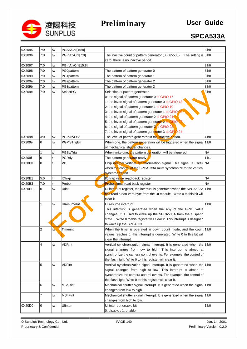
SPCA533A
© Sunplus Technology Co., Ltd.
Proprietary & Confidential
PAGE 140 Jun. 14, 2001
Preliminary Version: 0.2.0
Preliminary User Guide
0X2095 7:0 rw PGAtvCnt[15:8] 8’h0
0X2096 7:0 rw PGInAtvCnt[7:0] The inactive count of pattern generator (0 ~ 65535). The setting is
zero, there is no inactive period.
8’h0
0X2097 7:0 rw PGInAtvCnt[15:8] 8’h0
0X2098 7:0 rw PG0pattern The pattern of pattern generator 0 8’h0
0X2099 7:0 rw PG1pattern The pattern of pattern generator 1 8’h0
0X209a 7:0 rw PG2pattern The pattern of pattern generator 2 8’h0
0X209b 7:0 rw PG3pattern The pattern of pattern generator 3 8’h0
0X209c 7:0 rw SelectPG Selection of pattern generator
0: the signal of pattern generator 0 to GPIO 17
1: the invert signal of pattern generator 0 to GPIO 18
2: the signal of pattern generator 1 to GPIO 19
3: the invert signal of pattern generator 1 to GPIO 20
4: the signal of pattern generator 2 to GPIO 21
5: the invert signal of pattern generator 2 to GPIO 22
6: the signal of pattern generator 3 to GPIO 23
7: the invert signal of pattern generator 3 to GPIO 24
8’b0
0X209d 3:0 rw PGInAtvLev The level of pattern generator in the inactive period. 4’b0
0X209e 0 rw PGMSTrigEn When one, the pattern generation will be triggered when the signal
of mechanical shutter changes.
1’b0
1 w PGSwTrig When write one, the pattern generation will be triggered. NA
0X209f 0 r PGRdy The pattern generator ready 1’b1
0X20B0 0 r VD Chip internal vertical synchronization signal. This signal is useful
when the control of the SPCA533A must synchronize to the vertical
synchronization.
NA
0X20B1 5:0 r IOtrap IO trap value read-back register NA
0X20B3 7:0 r Probe Probe signal read back register NA
0X20C0 0 rw UIint UI interrupt register, the interrupt is generated when the SPCA533A
has read a non-zero byte from the UI module.. Write 0 to this bit will
clear it.
1’b0
1 rw UIresumeInt UI resume interrupt.
This interrupt is generated when the any of the GPIO value
changes. It is used to wake up the SPCA533A from the suspend
state. Write 0 to this register will clear it. This interrupt is designed
to wake up the SPCA533.
1’b0
2 rw Timerint When the timer is operated in down count mode, and the count
values reaches 0, this interrupt is generated. Write 0 to this bit will
clear the interrupt.
1’b0
4 rw VDRint Vertical synchronization signal interrupt. It is generated when the
signal changes from low to high. This interrupt is aimed at
synchronize the camera control events. For example, the control of
the flash light. Write 0 to this register will clear it.
1’b0
5 rw VDFint Vertical synchronization signal interrupt. It is generated when the
signal changes from high to low. This interrupt is aimed at
synchronize the camera control events. For example, the control of
the flash light. Write 0 to this register will clear it.
1’b0
6 rw MShRint Mechanical shutter signal interrupt. It is generated when the signal
changes from low to high.
1’b0
7 rw MShFint Mechanical shutter signal interrupt. It is generated when the signal
changes from high to low.
1’b0
0X20D0 0 rw UIinten UI interrupt enable bit
0: disable , 1: enable
1’b0

SPCA533A
© Sunplus Technology Co., Ltd.
Proprietary & Confidential
PAGE 141 Jun. 14, 2001
Preliminary Version: 0.2.0
Preliminary User Guide
1 rw UIRsminten UI resume interrupt enable bit
0: disable , 1: enable
1’b0
2 rw Timerinten Timer interrupt enable bit
0: disable
1: enable
1’b0
4 rw VDRinten VD rising edge interrupt enable bit
0: disable
1: enable
1’b0
5 rw VDFinten VD falling edge interrupt enable bit
0: disable
1: enable
1’b0
6 rw MShRinten Mechanical shutter control signal rising edge interrupt enable bit
0: disable
1: enable
1’b0
7 rw MSFinten Mechanical shutter control signal falling edge interrupt enable bit
0: disable
1: enable
1’b0
0X20E8 0 rw PGFRStart When set one, the pattern generator will be repeat forever. The
repeat count (register 0X2093) will be ignored.
1’b0
1 rw PGFRStop When set one, the pattern generator will be forced to reset state. If
the pattern generator is set to the repeat forever mode, only set the
bit to one to stop the repeat forever mode. The bit must be cleared
to zero when the pattern generator will be started again.
1’b0
2 reserved
3 rw USBPwrCfg 0: Bus-powered for USB getstatus command
1: Self-powered for USB getstatus command
1’b0
0X20FF 7:0 r RevID[7:0] Chip revision ID NA
2.3 CDSP Registers
Address bit attr name description Default
value
0X2100 0 rw pix_sw pixel switch for input image type 1’b1
1 rw line_sw line switch for input image type 1’b1
0X2103 7:0 rw hvalidshift Horizontal valid shift by CDSP 8’h24
0X2104 7:0 rw vvalidshift Vertical valid shift by CDSP 8’h16
0X2105 0 rw hmen Horizontal mirror enable (front 8, rear 16) 1’b0
0X210a 0 rw ObManuen Optical black manual reduction enable 1’b1
1 rw ObAutoen Optical black auto reduction enable 1’b0
2 rw CurrentFrameOb Current Frame OB 1’b0
6:4 rw Obtype OB Block Type (X x Y)
0: 1 x 256
1: 2 x 256
2: 4 x 256
3: 8 x 256
4: 256 x 1
5: 256 x 2
6: 256 x 4
7: 256 x 8
3’h0
0X210b 3:0 rw OBHoffH OB block horizontal offset (H) 4’h0
7:4 rw OBVoffH OB block vertical offset (H) 4’h0
0X210c 7:0 rw OBHoffL OB block horizontal offset (L) 8’h0
0X210d 7:0 rw OBVoffL OB block vertical offset (L) 8’h0

SPCA533A
© Sunplus Technology Co., Ltd.
Proprietary & Confidential
PAGE 142 Jun. 14, 2001
Preliminary Version: 0.2.0
Preliminary User Guide
0X210e 7:0 rw ManuOb[7:0] Manual optical black level 8’h20
0X210f 1:0 rw ManuOb[9:8] 2’h0
0X2110 0 rw BadPixFunEn Bad Pixel Compensation Function Enable 1‘b0
1 rw PgBPen Program bad pixel information to Bad Pixel SRAM; should be set to
0 when Bad Pixel Compensation Function Enable
1‘b0
2 rw PgBPRead When high, the bad pixel SRAM is in the read mode; otherwise the
bad pixel SRAM is in the write mode.
1‘b0
0X2111 7:0 rw BadPixInXL Bad Pixel download data X(L) 8‘h0
0X2112 3:0 rw BadPixInXH Bad Pixel download data X(H) 4‘h0
0X2113 7:0 rw BadPixInYL Bad Pixel download data Y(L) 8‘h0
0X2114 3:0 rw BadPixInYH Bad Pixel download data Y(H) 4‘h0
0X2115 7:0 rw BadPixAddr Bad Pixel SRAM Address
A write to this register will also trigger the actual action to write
download data X,Y to Bad Pixel SRAM when the register bit of
“PgBPRead” is 0.
8’h0
0X2116 7:0 r BadPixXL Bad Pixel SRAM data X(L) NA
0X2117 3:0 r BadPixXH Bad Pixel SRAM data X(H) NA
0X2118 7:0 r BadPixYL Bad Pixel SRAM data Y(L) NA
0X2119 3:0 r BadPixYH Bad Pixel SRAM data Y(H) NA
0X211a 0 rw RawDen Raw data scale function
0: disable
1: enable
1‘b0
1 rw RawDMode Raw data scale mode
0: drop pixel
1: filter pixel
1‘b0
0X211b 7:0 rw RawDF[7:0] Raw data scale factor (low byte) 8‘h0
0X211c 7:0 rw RawDF[15:8] Raw data scale factor (high byte) 8‘h0
0X211e 7:0 r AutoOb[7:0] Average optical black level of the built-in accumulator NA
0X211f 1:0 r AutoOb[9:8] NA
0X2120 7:0 rw Roffset R offset for white balance (1 sign +7 bit) 8’h8
0X2121 7:0 rw Groffset Gr offset for white balance (1 sign + 7 bit) 8’h0
0X2122 7:0 rw Boffset B offset for white balance (1 sign + 7 bit) 8’h4
0X2123 7:0 rw Gboffset Gb offset for white balance (1 sign + 7 bit) 8’h0
0X2124 7:0 rw Rgain(L) R gain for white balance (3.6 bit) (L byte) 8’ha5
0X2125 7:0 rw Grgain(L) Gr gain for white balance (3.6 bit) (L byte) 8’h40
0X2126 7:0 rw Bgain(L) B gain for white balance (3.6 bit) (L byte) 8’h5d
0X2127 7:0 rw Gbgain(L) Gb gain for white balance (3.6 bit) (L byte) 8’h40
0X2128 0 rw Gbgain(H) Gb gain for white balance (3.6 bit) (H byte) 1’b0
1 rw Bgain(H) B gain for white balance (3.6 bit) (H byte) 1’b0
2 rw Grgain(H) Gr gain for white balance (3.6 bit) (H byte) 1’b0
3 rw Rgain(H) R gain for white balance (3.6 bit) (H byte) 1’b0
0X2130 0 rw Romgammaen ROM Gamma Enable 1’b0
0X2140 7:0 rw A11(L) A11 coefficient for color correction (1 sign+2.6 bit) (Low byte) 8’h60
0X2141 7:0 rw A12(L) A12 coefficient for color correction (1 sign+2.6 bit) (Low byte) 8’hf0
0X2142 7:0 rw A13(L) A13 coefficient for color correction (1 sign+2.6 bit) (Low byte) 8’hf0
0X2143 7:0 rw A21(L) A21 coefficient for color correction (1 sign+2.6 bit) (Low byte) 8’hf0
0X2144 7:0 rw A22(L) A22 coefficient for color correction (1 sign+2.6 bit) (Low byte) 8’h60
0X2145 7:0 rw A23(L) A23 coefficient for color correction (1 sign+2.6 bit) (Low byte) 8’hf0
0X2146 7:0 rw A31(L) A31 coefficient for color correction (1 sign+2.6 bit) (Low byte) 8’hf0
0X2147 7:0 rw A32(L) A32 coefficient for color correction (1 sign+2.6 bit) (Low byte) 8’hf0
0X2148 7:0 rw A33(L) A33 coefficient for color correction (1 sign+2.6 bit) (Low byte) 8’h60

SPCA533A
© Sunplus Technology Co., Ltd.
Proprietary & Confidential
PAGE 143 Jun. 14, 2001
Preliminary Version: 0.2.0
Preliminary User Guide
0X2149 7:0 rw A32,A31,A23,A22,A21,A13,
A12,A11(H)
A32~A11 coefficient for color correction (1 sign+2.6 bit) (H byte) 8’hee
0X214a 0 rw A33(H) A33 coefficient for color correction (1 sign+2.6 bit) (H byte) 1’b0
0X2150 1:0 rw LutGammaMode LUT gamma mode
0: disable
1: enable LUT gamma
2: enable LUT gamma with low pass filter
2’h2
0X2151 7:0 rw Gammalfd The point distance in the low pass filter of LUT gamma. 8’h20
0X2160 7:0 rw Ylut0 Y look-up table for gamma correction (unit: 4) 8’h0
0X2161 7:0 rw Ylut1 8’h17
0X2162 7:0 rw Ylut2 8’h4a
0X2163 7:0 rw Ylut3 8’h69
0X2164 7:0 rw Ylut4 8’h83
0X2165 7:0 rw Ylut5 8’h99
0X2166 7:0 rw Ylut6 8’hab
0X2167 7:0 rw Ylut7 8’hbb
0X2168 7:0 rw Ylut8 8’hc7
0X2169 7:0 rw Ylut9 8’hd1
0X216a 7:0 rw Ylut10 8’hd9
0X216b 7:0 rw Ylut11 8’he0
0X216c 7:0 rw Ylut12 8’he7
0X216d 7:0 rw Ylut13 8’hee
0X216e 7:0 rw Ylut14 8’hf5
0X216f 7:0 rw Ylut15 8’hfc
0X2170 7:0 rw Ylut16 8’hff
0X2180 3:0 rw Fh00 The factor of horizontal edge filter
[3]: sign bit (0: positive, 1:negtive)
[2:0]: magnitude
0: 0
1: 1
2: 2
3: 3
4: 4
4’h0
7:4 rw Fh01 4’h0
0X2181 3:0 rw Fh02 4’h0
7:4 rw Fh03 4’h0
0X2182 3:0 rw Fh04 4’h0
7:4 rw Fh10 4’h0
0X2183 3:0 rw Fh11 4’h9
7:4 rw Fh12 The factor of horizontal edge filter
[3]: sign bit (0: positive, 1:negtive)
[2:0]: magnitude
0: 0
1: 1
2: 2
3: 3
4: 4
5: 8
6: 16
4’h9
0X2184 3:0 rw Fh13 4’h9
7:4 rw Fh14 4’h0
0X2185 3:0 rw Fh20 4’h0

SPCA533A
© Sunplus Technology Co., Ltd.
Proprietary & Confidential
PAGE 144 Jun. 14, 2001
Preliminary Version: 0.2.0
Preliminary User Guide
7:4 rw Fh21 4’h9
0X2186 3:0 rw Fh22 The factor of horizontal edge filter
[3]: sign bit (0: positive, 1:negtive)
[2:0]: magnitude
0: 0
1: 1
2: 2
3: 3
4: 4
5: 8
6: 16
4’h5
7:4 rw Fh23 4’h9
0X2187 3:0 rw Fh24 4’h0
7:4 rw Fh30 4’h0
0X2188 3:0 rw Fh31 4’h9
7:4 rw Fh32 The factor of horizontal edge filter
[3]: sign bit (0: positive, 1:negtive)
[2:0]: magnitude
0: 0
1: 1
2: 2
3: 3
4: 4
5: 8
6: 16
4’h9
0X2189 3:0 rw Fh33 4’h9
7:4 rw Fh34 4’h0
0X218a 3:0 rw Fh40 4’h0
7:4 rw Fh41 4’h0
0X218b 3:0 rw Fh42 The factor of horizontal edge filter
[3]: sign bit (0: positive, 1:negtive)
[2:0]: magnitude
0: 0
1: 1
2: 2
3: 3
4: 4
5: 8
6: 16
4’h0
7:4 rw Fh43 4’h0
0X218c 3:0 rw Fh44 4’h0
6:4 rw Fha The division factor of horizontal edge filter
0: 1
1: 2
2: 4
3: 8
4: 16
5: 32
6: 64
7: 128
3’h4
0X2190 3:0 rw Fv00 The factor of vertical edge filter
[3]: sign bit (0: positive, 1:negtive)
[2:0]: magnitude
8’h0
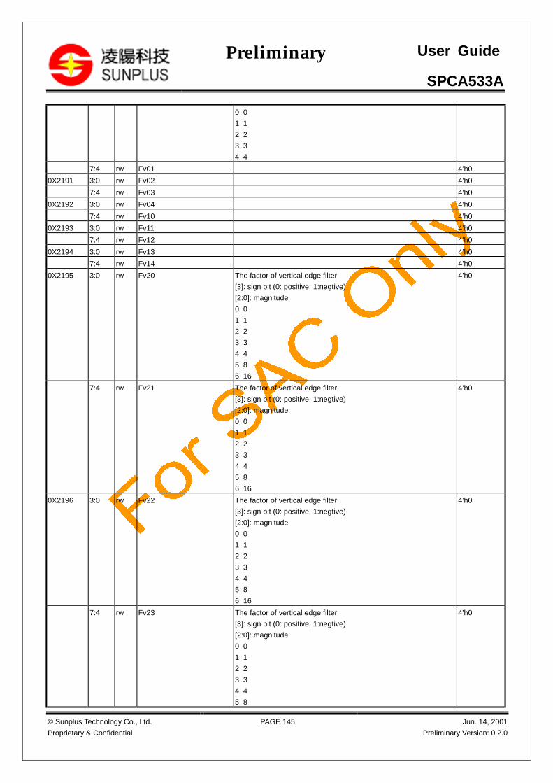
SPCA533A
© Sunplus Technology Co., Ltd.
Proprietary & Confidential
PAGE 145 Jun. 14, 2001
Preliminary Version: 0.2.0
Preliminary User Guide
0: 0
1: 1
2: 2
3: 3
4: 4
7:4 rw Fv01 4’h0
0X2191 3:0 rw Fv02 4’h0
7:4 rw Fv03 4’h0
0X2192 3:0 rw Fv04 4’h0
7:4 rw Fv10 4’h0
0X2193 3:0 rw Fv11 4’h0
7:4 rw Fv12 4’h0
0X2194 3:0 rw Fv13 4’h0
7:4 rw Fv14 4’h0
0X2195 3:0 rw Fv20 The factor of vertical edge filter
[3]: sign bit (0: positive, 1:negtive)
[2:0]: magnitude
0: 0
1: 1
2: 2
3: 3
4: 4
5: 8
6: 16
4’h0
7:4 rw Fv21 The factor of vertical edge filter
[3]: sign bit (0: positive, 1:negtive)
[2:0]: magnitude
0: 0
1: 1
2: 2
3: 3
4: 4
5: 8
6: 16
4’h0
0X2196 3:0 rw Fv22 The factor of vertical edge filter
[3]: sign bit (0: positive, 1:negtive)
[2:0]: magnitude
0: 0
1: 1
2: 2
3: 3
4: 4
5: 8
6: 16
4’h0
7:4 rw Fv23 The factor of vertical edge filter
[3]: sign bit (0: positive, 1:negtive)
[2:0]: magnitude
0: 0
1: 1
2: 2
3: 3
4: 4
5: 8
4’h0

SPCA533A
© Sunplus Technology Co., Ltd.
Proprietary & Confidential
PAGE 146 Jun. 14, 2001
Preliminary Version: 0.2.0
Preliminary User Guide
6: 16
0X2197 3:0 rw Fv24 The factor of vertical edge filter
[3]: sign bit (0: positive, 1:negtive)
[2:0]: magnitude
0: 0
1: 1
2: 2
3: 3
4: 4
5: 8
6: 16
4’h0
7:4 rw Fv30 4’h0
0X2198 3:0 rw Fv31 4’h0
7:4 rw Fv32 4’h0
0X2199 3:0 rw Fv33 4’h0
7:4 rw Fv34 4’h0
0X219a 3:0 rw Fv40 4’h0
7:4 rw Fv41 4’h0
0X219b 3:0 rw Fv42 4’h0
7:4 rw Fv43 4’h0
0X219c 3:0 rw Fv44 4’h0
6:4 rw Fva The division factor of vertical edge filter
0: 1
1: 2
2: 4
3: 8
4: 16
5: 32
6: 64
7: 128
3’h0
0X21a0 0 rw YedgeEn Y Edge Enable 1’b1
0X21a5 1:0 rw YhAvgMode Y horizontal average mode
00: no average
01: 2 pixel average
10: 3 pixel average
11: 4 pixel average
2’b0
0X21a6 0 rw BTCTEn Brightness and Contrast adjustment enable 1’b0
0X21a7 7:0 rw BT Brightness adjustment (1 sign+7 bit, unit 2) 8’h0
0X21a8 7:0 rw CT Contrast adjustment (3.5 bit) 8’h20
0X21ab 0 rw UVHAvg UV Horizontal Average 1’b1
1 rw UVVAvg UV Vertical Average 1’b1
0X21ac 0 rw STHueEn Saturation and Hue adjustment enable 1’b0
7:6 rw Hue(H) Hue adjustment (H byte) 2’h0
0X21ad 7:0 rw Hue(L) Hue adjustment (L byte) (divide by 2 = degree) 8’h00
0X21ae 7:0 rw Sat Saturation adjustment (3.5 bit) 8’h20
2.4 CDSP Window Registers
Address bit attr name description Default
value
0X2200 7:0 rw HwdOffset Window horizontal offset 8’h1b
0X2201 7:0 rw VwdOffset Window vertical offset 8’h15

SPCA533A
© Sunplus Technology Co., Ltd.
Proprietary & Confidential
PAGE 147 Jun. 14, 2001
Preliminary Version: 0.2.0
Preliminary User Guide
0X2202 6:0 rw HwdSize Window horizontal size 7’h33
0X2203 7:0 rw VwdSize[7:0] Window vertical size 8’h26
0X2204 1:0 rw VwdSize[9:8] 2’h0
0X2205 2:0 rw PseudoHwdSize Pseudo Horizontal Window Size
(Horizontal Accumulator Normalizing Factor)
0: 8
1: 16
2: 32
3: 64
4: 128
3’h3
6:4 rw PseudoVwdSize Pseudo Vertical Window Size
(Vertical Accumulator Normalizing Factor)
0: 8
1: 16
2: 32
3: 64
4: 128
5: 256
6: 512
7: 1024
3’h3
0X2206 0 rw windowhold When one, the window value will be held. 1’b0
1 rw wbrbclampen White Balance RB clamping enable 1’b1
2 rw WBYThrEn White Balance Y threshold enable 1’b1
0X2207 7:0 rw WB_RBClamp RB clamp value for white balance 8’hc8
0X2208 7:0 rw WB_YthrL Low luminance threshold for white balance (unit: 4) 8’h32
0X2209 7:0 rw WB_YthrH High luminance threshold for white balance (unit: 4) 8’hc8
0X2210 7:0 rw AFWOffX[7:0] Focus measurement window X offset 8’h61
0X2211 7:0 rw AFWOffY[7:0] Focus measurement window Y offset 8’h36
0X2212 0 rw AFWOffX[8] 1’b0
7:4 rw AFWOffY[11:8] 2’h0
0X2213 7:0 rw AFWX[7:0] Focus measurement window X size 8’h80
0X2214 7:0 rw AFWY[7:0] Focus measurement window Y size 8’h80
0X2215 0 rw AFWX[8] 1’b0
7:4 rw AFWY[11:8] 4’h0
0X2216 2:0 rw PAFWXAccF Pseudo AF Window X Size
(Horizontal Accumulator Normalizing Factor)
0: 8
1: 16
2: 32
3: 64
4: 128
5: 256
6: 512
3’h4
7:4 rw PAFWYAccF Pseudo AF Vertical Window Size
(Vertical Accumulator Normalizing Factor)
0: 8
1: 16
2: 32
3: 64
4: 128
5: 256
6: 512
4’h4

SPCA533A
© Sunplus Technology Co., Ltd.
Proprietary & Confidential
PAGE 148 Jun. 14, 2001
Preliminary Version: 0.2.0
Preliminary User Guide
7: 1024
8: 2048
9: 4096
0X2217 7:0 r AFWDO [7:0] Focus measurement window out NA
0X2218 4:0 r AFWDO[12:8] NA
0X2280 7:0 r YWD11 Y window 11 data (unit: 4) NA
0X2281 7:0 r YWD12 Y window 12 data (unit: 4) NA
0X2282 7:0 r YWD13 Y window 13 data (unit: 4) NA
0X2283 7:0 r YWD14 Y window 14 data (unit: 4) NA
0X2284 7:0 r YWD15 Y window 15 data (unit: 4) NA
0X2285 7:0 r YWD21 Y window 21 data (unit: 4) NA
0X2286 7:0 r YWD22 Y window 22 data (unit: 4) NA
0X2287 7:0 r YWD23 Y window 23 data (unit: 4) NA
0X2288 7:0 r YWD24 Y window 24 data (unit: 4) NA
0X2289 7:0 r YWD25 Y window 25 data (unit: 4) NA
0X228a 7:0 r YWD31 Y window 31 data (unit: 4) NA
0X228b 7:0 r YWD32 Y window 32 data (unit: 4) NA
0X228c 7:0 r YWD33 Y window 33 data (unit: 4) NA
0X228d 7:0 r YWD34 Y window 34 data (unit: 4) NA
0X228e 7:0 r YWD35 Y window 35 data (unit: 4) NA
0X228f 7:0 r YWD41 Y window 41 data (unit: 4) NA
0X2290 7:0 r YWD42 Y window 42 data (unit: 4) NA
0X2291 7:0 r YWD43 Y window 43 data (unit: 4) NA
0X2292 7:0 r YWD44 Y window 44 data (unit: 4) NA
0X2293 7:0 r YWD45 Y window 45 data (unit: 4) NA
0X2294 7:0 r YWD51 Y window 51 data (unit: 4) NA
0X2295 7:0 r YWD52 Y window 52 data (unit: 4) NA
0X2296 7:0 r YWD53 Y window 53 data (unit: 4) NA
0X2297 7:0 r YWD54 Y window 54 data (unit: 4) NA
0X2298 7:0 r YWD55 Y window 55 data (unit: 4) NA
0X2299 7:0 r YWDAvg Y window average (unit: 4) NA
0X22a0 7:0 r RYWD11[7:0] RY window 11 data (unit: 4) NA
0X22a1 7:0 r RYWD12[7:0] RY window 12 data (unit: 4) NA
0X22a2 7:0 r RYWD13[7:0] RY window 13 data (unit: 4) NA
0X22a3 7:0 r RYWD14[7:0] RY window 14 data (unit: 4) NA
0X22a4 7:0 r RYWD15[7:0] RY window 15 data (unit: 4) NA
0X22a5 7:0 r RYWD21[7:0] RY window 21 data (unit: 4) NA
0X22a6 7:0 r RYWD22[7:0] RY window 22 data (unit: 4) NA
0X22a7 7:0 r RYWD23[7:0] RY window 23 data (unit: 4) NA
0X22a8 7:0 r RYWD24[7:0] RY window 24 data (unit: 4) NA
0X22a9 7:0 r RYWD25[7:0] RY window 25 data (unit: 4) NA
0X22aa 7:0 r RYWD31[7:0] RY window 31 data (unit: 4) NA
0X22ab 7:0 r RYWD32[7:0] RY window 32 data (unit: 4) NA
0X22ac 7:0 r RYWD33[7:0] RY window 33 data (unit: 4) NA
0X22ad 7:0 r RYWD34[7:0] RY window 34 data (unit: 4) NA
0X22ae 7:0 r RYWD35[7:0] RY window 35 data (unit: 4) NA
0X22af 7:0 r RYWD41[7:0] RY window 41 data (unit: 4) NA
0X22b0 7:0 r RYWD42[7:0] RY window 42 data (unit: 4) NA
0X22b1 7:0 r RYWD43[7:0] RY window 43 data (unit: 4) NA
0X22b2 7:0 r RYWD44[7:0] RY window 44 data (unit: 4) NA
0X22b3 7:0 r RYWD45[7:0] RY window 45 data (unit: 4) NA

SPCA533A
© Sunplus Technology Co., Ltd.
Proprietary & Confidential
PAGE 149 Jun. 14, 2001
Preliminary Version: 0.2.0
Preliminary User Guide
0X22b4 7:0 r RYWD51[7:0] RY window 51 data (unit: 4) NA
0X22b5 7:0 r RYWD52[7:0] RY window 52 data (unit: 4) NA
0X22b6 7:0 r RYWD53[7:0] RY window 53 data (unit: 4) NA
0X22b7 7:0 r RYWD54[7:0] RY window 54 data (unit: 4) NA
0X22b8 7:0 r RYWD55[7:0] RY window 55 data (unit: 4) NA
0X22b9 7:0 r RYWDSign[7:0] RY window 11 to 15 and window 21 to 23 sign bit NA
0X22ba 7:0 r RYWDSign[15:8] RY window 24 to 25, window 31 to 35 and window 41 sign bit NA
0X22bb 7:0 r RYWDSign
[23:16]
RY window 42 to 45 and window 51 to 54 sign bit NA
0X22bc 0 r RYWDSign[24] RY window 55 sign bit NA
0X22bd 7:0 r RYWDAvg[7:0] RY window average (unit: 4) NA
0X22be 0 r RYWDAvg[8] NA
0X22c0 7:0 r BYWD11[7:0] BY window 11 data (unit: 4) NA
0X22c1 7:0 r BYWD12[7:0] BY window 12 data (unit: 4) NA
0X22c2 7:0 r BYWD13[7:0] BY window 13 data (unit: 4) NA
0X22c3 7:0 r BYWD14[7:0] BY window 14 data (unit: 4) NA
0X22c4 7:0 r BYWD15[7:0] BY window 15 data (unit: 4) NA
0X22c5 7:0 r BYWD21[7:0] BY window 21 data (unit: 4) NA
0X22c6 7:0 r BYWD22[7:0] BY window 22 data (unit: 4) NA
0X22c7 7:0 r BYWD23[7:0] BY window 23 data (unit: 4) NA
0X22c8 7:0 r BYWD24[7:0] BY window 24 data (unit: 4) NA
0X22c9 7:0 r BYWD25[7:0] BY window 25 data (unit: 4) NA
0X22ca 7:0 r BYWD31[7:0] BY window 31 data (unit: 4) NA
0X22cb 7:0 r BYWD32[7:0] BY window 32 data (unit: 4) NA
0X22cc 7:0 r BYWD33[7:0] BY window 33 data (unit: 4) NA
0X22cd 7:0 r BYWD34[7:0] BY window 34 data (unit: 4) NA
0X22ce 7:0 r BYWD35[7:0] BY window 35 data (unit: 4) NA
0X22cf 7:0 r BYWD41[7:0] BY window 41 data (unit: 4) NA
0X22d0 7:0 r BYWD42[7:0] BY window 42 data (unit: 4) NA
0X22d1 7:0 r BYWD43[7:0] BY window 43 data (unit: 4) NA
0X22d2 7:0 r BYWD44[7:0] BY window 44 data (unit: 4) NA
0X22d3 7:0 r BYWD45[7:0] BY window 45 data (unit: 4) NA
0X22d4 7:0 r BYWD51[7:0] BY window 51 data (unit: 4) NA
0X22d5 7:0 r BYWD52[7:0] BY window 52 data (unit: 4) NA
0X22d6 7:0 r BYWD53[7:0] BY window 53 data (unit: 4) NA
0X22d7 7:0 r BYWD54[7:0] BY window 54 data (unit: 4) NA
0X22d8 7:0 r BYWD55[7:0] BY window 55 data (unit: 4) NA
0X22d9 7:0 r BYWDSign[7:0] BY window 11 to 15 and window 21 to 23 sign bit NA
0X22da 7:0 r BYWDSign[15:8] BY window 24 to 25, window 31 to 35 and window 41 sign bit NA
0X22db 7:0 r BYWDSign
[23:16]
BY window 42 to 45 and window 51 to 54 sign bit NA
0X22dc 0 r BYWDSign[24] BY window 55 sign bit NA
0X22dd 7:0 r BYWDAvg[7:0] BY window average (unit: 4) NA
0X22de 0 r BYWDAvg[8] NA
2.5 DMA Controller Registers
Address bit Attr Name DescriptionDefault
value
0X2300 7:0 r/w DMAdata DMA data port NA
0X2301 2:0 r/w DMAsrc DMA source(provider) selection:
0: DRAM controller
3’b0
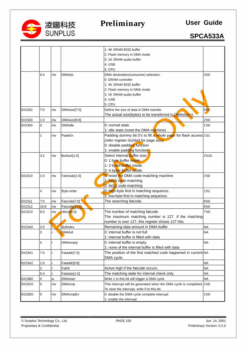
SPCA533A
© Sunplus Technology Co., Ltd.
Proprietary & Confidential
PAGE 150 Jun. 14, 2001
Preliminary Version: 0.2.0
Preliminary User Guide
1: 4K SRAM 8032 buffer
2: Flash memory in DMA mode
3: 1K SRAM audio buffer
4: USB
5: CPU
6:4 r/w DMAdst DMA destination(consumer) selection:
0: DRAM controller
1: 4K SRAM 8032 buffer
2: Flash memory in DMA mode
3: 1K SRAM audio buffer
4: USB
5: CPU
3’b0
0X2302 7:0 r/w DMAsize[7:0] Define the size of data in DMA transfer.
The actual size(bytes) to be transferred is DMAsize+1.8’b0
0X2303 1:0 r/w DMAsize[9:8] 2’b0
0X2304 0 r/w DMAidle 0: normal state1: idle state (reset the DMA machine)
1’b0
1 r/w PadeEn Padding dummy bit 0’s to fill a whole page for flash access(refer register 0x24a3 for page size)0: disable padding function1: enable padding function
1’b1
3:2 r/w Bufsize[1:0] Select internal buffer size:0: 1 byte buffer inside.1: 2 bytes buffer inside.2: 4 bytes buffer inside.
2’b10
0X2310 1:0 r/w Fatmode[1:0] 0: reset the DMA code-matching machine.1: fat16 code-matching2: fat12 code-matching
2’b0
4 r/w Byte-order 0: high-byte first in matching sequence.1: low-byte first in matching sequence.
1’b1
0X2311 7:0 r/w Fatcode[7:0] The searching fatcode. 8’b0
0X2312 15:8 r/w Fatcode[15:8] 8’b0
0X2313 6:0 r/w Hitcnt[6:0] The number of matching fatcode.The maximum matching number is 127. If the matchingnumber is over 127, this register shows 127 hits.
7’b0
0X23A0 2:0 r Bufindex Remaining data amount in DMA buffer NA
3 r DMAfull 0: internal buffer is not full1: internal buffer is filled with data
NA
4 r DMAempty 0: internal buffer is empty1: none of the internal buffer is filled with data
NA
0X23A1 7:0 r Fataddr[7:0] The position of the first matched code happened in currentDMA cycle.
NA
0X23A2 1:0 r Fataddr[9:8] NA
2 r Fathit Active high if the fatcode occurs. NA
5:4 r Fatstate[1:0] The matching state for internal check only. NA
0X23B0 0 w DMAstart Write 1 to this bit will trigger a DMA cycle NA
0X23C0 0 r/w DMAcmp This interrupt will be generated when the DMA cycle is completed.
To clear the interrupt, write 0 to this bit.
1’b0
0X23D0 0 r/w DMAcmpEn 0: disable the DMA cycle complete interrupt
1: enable the interrupt
1’b0
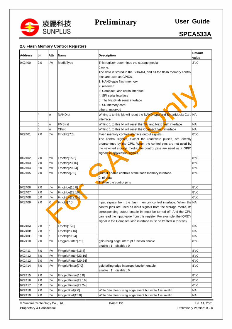
SPCA533A
© Sunplus Technology Co., Ltd.
Proprietary & Confidential
PAGE 151 Jun. 14, 2001
Preliminary Version: 0.2.0
Preliminary User Guide
2.6 Flash Memory Control Registers
Address bit Attr Name DescriptionDefault
value
0X2400 2:0 r/w MediaType This register determines the storage media
0:none.
The data is stored in the SDRAM, and all the flash memory control
pins are used as GPIOs.
1: NAND-gate flash memory
2: reserved
3: CompactFlash cards interface
4: SPI serial interface
5: The NextFlah serial interface
6. SD memory card
others: reserved
3’b0
4 w NANDrst Writing 1 to this bit will reset the NAND type and SmartMedia Card
interface
NA
5 w FMSIrst Writing 1 to this bit will reset the SPI and Next flash interface NA
6 w CFrst Writing 1 to this bit will reset the Compact flash interface NA
0X2401 7:0 r/w Fmctrlo[7:0] Flash memory control interface output signals.
The control signals, except the read/write pulses, are directly
programmed by the CPU. When the control pins are not used by
the selected storage media, the control pins are used as a GPIO
signals in application signals.
8’b0
0X2402 7:0 r/w Fmctrlo[15:8] 8’b0
0X2403 7:0 r/w Fmctrlo[23:16] 8’b0
0X2404 5:0 r/w Fmctrlo[29:24] 6’b0
0X2405 7:0 r/w Fmctrloe[7:0] Output enable controls of the flash memory interface.
0: tri-state
1: drive the control pins
8’b0
0X2406 7:0 r/w Fmctrloe[15:8] 8’b0
0X2407 7:0 r/w Fmctrloe[23:16] 8’b0
0X2408 5:0 r/w Fmctrloe[29:24] 6’b0
0X2409 7:0 R Fmctrli[7:0] Input signals from the flash memory control interface. When the
control pins are used as input signals from the storage media, its
corresponding output enable bit must be turned off. And the CPU
can read the input value from this register. For example, the IORDY
signal in the CompactFlash interface must be treated in this way.
NA
0X240A 7:0 r Fmctrli[15:8] NA
0X240B 7:0 r Fmctrli[23:16] NA
0X240C 5:0 r Fmctrli[29:24] NA
0X2410 7:0 r/w FmgpioRinten[7:0] gpio rising edge interrupt function enable
enable : 1 disable : 0
8’b0
0X2411 7:0 r/w FmgpioRinten[15:8] 8’b0
0X2412 7:0 r/w FmgpioRinten[23:16] 8’b0
0X2413 5:0 r/w FmgpioRinten[29:24] 6’b0
0X2414 7:0 r/w FmgpioFinten[7:0] gpio falling edge interrupt function enable
enable : 1 disable : 0
8’b0
0X2415 7:0 r/w FmgpioFinten[15:8] 8’b0
0X2416 7:0 r/w FmgpioFinten[23:16] 8’b0
0X2417 5:0 r/w FmgpioFinten[29:24] 6’b0
0X2418 7:0 r/w FmgpioRint[7:0] Write 0 to clear rising edge event but write 1 is invalid NA
0X2419 7:0 r/w FmgpioRint[15:8] Write 0 to clear rising edge event but write 1 is invalid NA
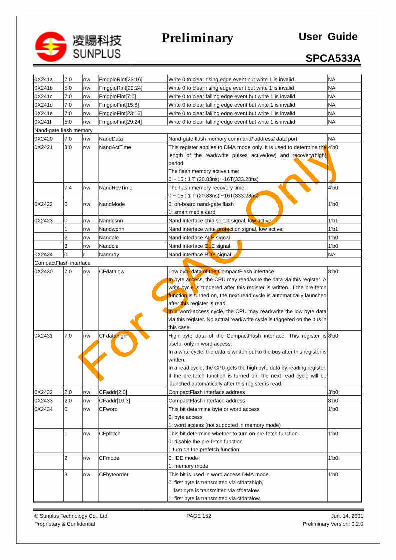
SPCA533A
© Sunplus Technology Co., Ltd.
Proprietary & Confidential
PAGE 152 Jun. 14, 2001
Preliminary Version: 0.2.0
Preliminary User Guide
0X241a 7:0 r/w FmgpioRint[23:16] Write 0 to clear rising edge event but write 1 is invalid NA
0X241b 5:0 r/w FmgpioRint[29:24] Write 0 to clear rising edge event but write 1 is invalid NA
0X241c 7:0 r/w FmgpioFint[7:0] Write 0 to clear falling edge event but write 1 is invalid NA
0X241d 7:0 r/w FmgpioFint[15:8] Write 0 to clear falling edge event but write 1 is invalid NA
0X241e 7:0 r/w FmgpioFint[23:16] Write 0 to clear falling edge event but write 1 is invalid NA
0X241f 5:0 r/w FmgpioFint[29:24] Write 0 to clear falling edge event but write 1 is invalid NA
Nand-gate flash memory
0X2420 7:0 r/w NandData Nand-gate flash memory command/ address/ data port NA
0X2421 3:0 r/w NandActTime This register applies to DMA mode only. It is used to determine the
length of the read/write pulses active(low) and recovery(high)
period.
The flash memory active time:
0 ~ 15 : 1 T (20.83ns) ~16T(333.28ns)
4’b0
7:4 r/w NandRcvTime The flash memory recovery time:
0 ~ 15 : 1 T (20.83ns) ~16T(333.28ns)
4’b0
0X2422 0 r/w NandMode 0: on-board nand-gate flash
1: smart media card
1’b0
0X2423 0 r/w Nandcsnn Nand interface chip select signal, low active 1’b1
1 r/w Nandwpnn Nand interface write protection signal, low active 1’b1
2 r/w Nandale Nand interface ALE signal 1’b0
3 r/w Nandcle Nand interface CLE signal 1’b0
0X2424 0 r Nandrdy Nand interface RDY signal NA
CompactFlash interface
0X2430 7:0 r/w CFdatalow Low byte data of the CompactFlash interface
In byte access, the CPU may read/write the data via this register. A
write cycle is triggered after this register is written. If the pre-fetch
function is turned on, the next read cycle is automatically launched
after this register is read.
In a word-access cycle, the CPU may read/write the low byte data
via this register. No actual read/write cycle is triggered on the bus in
this case.
8’b0
0X2431 7:0 r/w CFdatahigh High byte data of the CompactFlash interface. This register is
useful only in word access.
In a write cycle, the data is written out to the bus after this register is
written.
In a read cycle, the CPU gets the high byte data by reading register.
If the pre-fetch function is turned on, the next read cycle will be
launched automatically after this register is read.
8’b0
0X2432 2:0 r/w CFaddr[2:0] CompactFlash interface address 3’b0
0X2433 2:0 r/w CFaddr[10:3] CompactFlash interface address 8’b0
0X2434 0 r/w CFword This bit determine byte or word access
0: byte access
1: word access (not suppoted in memory mode)
1’b0
1 r/w CFpfetch This bit determine whether to turn on pre-fetch function
0: disable the pre-fetch function
1:turn on the prefetch function
1’b0
2 r/w CFmode 0: IDE mode
1: memory mode
1’b0
3 r/w CFbyteorder This bit is used in word access DMA mode.
0: first byte is transmitted via cfdatahigh,
last byte is transmitted via cfdatalow.
1: first byte is transmitted via cfdatalow,
1’b0

SPCA533A
© Sunplus Technology Co., Ltd.
Proprietary & Confidential
PAGE 153 Jun. 14, 2001
Preliminary Version: 0.2.0
Preliminary User Guide
last byte is transmitted via cfdatahigh.
0X2435 3:0 r/w Cfpulswd[3:0] Active time of the CFwrnn / CFrdnn signal.
0: 1 clock cycle
1: 2 clock cycle
2: 3 clock cycle
………………..
f: 16 clock cycle
4’b0
7:4 r/w Cfrcvtime[3:0] Recovery time of the CFwrnn / CFrdnn signal.
0: 1 clock cycle
1: 2 clock cycle
2: 3 clock cycle
………………..
f: 16 clock cycle
4’b0
0X2436 1:0 r/w CFcs[1:0] CompactFlash interface chip select
In true IDE mode, CFcs[1:0] controls the pins ‘CS1/’ and ‘CS2/’.
In memory mode, only CFcs[0] controls the pin ’CE/’.
2’b11
0X2439 0 r/w CFregnn CF interface reg signal
This register is only applied to memory mode, and it controls the pin
‘REG/’.
1’b1
0X243a 0 r/w CFrstnn CompactFlash interface reset signal 1’b1
0X243b 0 r CFready CompactFlash interface ready
0: The CompactFlash interface is busy and the CPU must wait
1: The CPU may read/write the data port
1’b1
0X243c 0 r CFrdybsynn This is a status pin routed directly from the CompactFlash card NA
Serial interface (including the SPI Serial interface and the NextFlash serial interface)
0X2440 7:0 r/w FMsitxd[7:0] Serial flash memory TX data port 8’b0
0X2441 7:0 r FMsirxd[7:0] Serial flash memory RX data port. Reading from this register will
get the data received from the serial flash memory. No serial clock
timing is asserted.
8’b0
0X2442 7:0 r FMsiprx[7:0] Reading from this register will get the data received from the serial
flash memory. It will also invoke a read timing to pre-fetch the next
byte of data.
8’b0
0X2443 7:0 r FMsiprx1[7:0] Reading from this register causes the SPCA533A to assert the first
serial clock to the flash memory. The data being read could be
discarded. It is aimed to meeting the timing requirement for reading
the NextFlash status word. The CPU should wait 30 ~ 100 us after
reading this register.
8’b0
0X2444 7:0 r FMsiprx7[7:0] After this register is read, the SPCA533A asserts the remaing 7
clocks to get the 2nd status byte of the NextFlash serial flash
memory. The CPU may read the Fmsirxd register to get the status
word after the FMSIbusy status is de-asserted.
8’b0
0X2446 1:0 r/w FMSIfreq[1:0] Serial clock frequency selecton
If NextFlash
0: 24 MHz
1: 12 MHz
2: 8 MHz
3: 6 MHz
If SPI
0: 12 MHz
1: 6MHz
2: 3MHz
3: 200 KHz
2’b0
0X2447 0 r/w FMSIdoenn Nextflash data output enable 1’b1
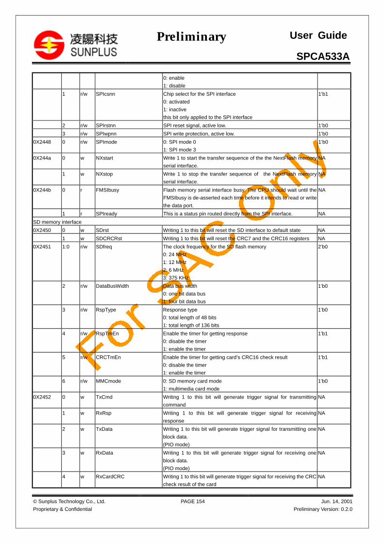
SPCA533A
© Sunplus Technology Co., Ltd.
Proprietary & Confidential
PAGE 154 Jun. 14, 2001
Preliminary Version: 0.2.0
Preliminary User Guide
0: enable
1: disable
1 r/w SPIcsnn Chip select for the SPI interface
0: activated
1: inactive
this bit only applied to the SPI interface
1’b1
2 r/w SPIrstnn SPI reset signal, active low. 1’b0
3 r/w SPIwpnn SPI write protection, active low. 1’b0
0X2448 0 r/w SPImode 0: SPI mode 0
1: SPI mode 3
1’b0
0X244a 0 w NXstart Write 1 to start the transfer sequence of the the NextFlash memory
serial interface.
NA
1 w NXstop Write 1 to stop the transfer sequence of the NextFlash memory
serial interface.
NA
0X244b 0 r FMSIbusy Flash memory serial interface busy. The CPU should wait until the
FMSIbusy is de-asserted each time before it intends to read or write
the data port.
NA
1 r SPIready This is a status pin routed directly from the SPI interface. NA
SD memory interface
0X2450 0 w SDrst Writing 1 to this bit will reset the SD interface to default state NA
1 w SDCRCRst Writing 1 to this bit will reset the CRC7 and the CRC16 registers NA
0X2451 1:0 r/w SDfreq The clock frequency for the SD flash memory
0: 24 MHz
1: 12 MHz
2: 6 MHz
3: 375 KHz
2’b0
2 r/w DataBusWidth Data bus width
0: one bit data bus
1: four bit data bus
1’b0
3 r/w RspType Response type
0: total length of 48 bits
1: total length of 136 bits
1’b0
4 r/w RspTmEn Enable the timer for getting response
0: disable the timer
1: enable the timer
1’b1
5 r/w CRCTmEn Enable the timer for getting card’s CRC16 check result
0: disable the timer
1: enable the timer
1’b1
6 r/w MMCmode 0: SD memory card mode
1: multimedia card mode
1’b0
0X2452 0 w TxCmd Writing 1 to this bit will generate trigger signal for transmitting
command
NA
1 w RxRsp Writing 1 to this bit will generate trigger signal for receiving
response
NA
2 w TxData Writing 1 to this bit will generate trigger signal for transmitting one
block data.
(PIO mode)
NA
3 w RxData Writing 1 to this bit will generate trigger signal for receiving one
block data.
(PIO mode)
NA
4 w RxCardCRC Writing 1 to this bit will generate trigger signal for receiving the CRC
check result of the card
NA
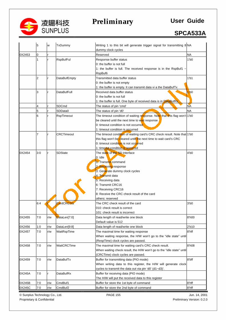
SPCA533A
© Sunplus Technology Co., Ltd.
Proprietary & Confidential
PAGE 155 Jun. 14, 2001
Preliminary Version: 0.2.0
Preliminary User Guide
5 w TxDummy Writing 1 to this bit will generate trigger signal for transmitting 8
dummy clock cycles
NA
0X2453 0 r Reserved NA
1 r RspBufFul Response buffer status
0: the buffer is not full
1: the buffer is full. The received response is in the RspBuf1 ~
RspBuf6
1’b0
2 r DataBufEmpty Transmitted data buffer status
0: the buffer is not empty
1: the buffer is empty. It can transmit data vi a the DataBufTx
1’b1
3 r DataBufFull Received data buffer status
0: the buffer is not full
1: the buffer is full. One byte of received data is in DataBufRx
1’b0
4 r SDCmd The status of pin ‘cmd’ NA
5 r SDData0 The status of pin ‘d0’ NA
6 r RspTimeout The timeout condition of waiting response. Note that this flag won’t
be cleared until the next time to wait response
0: timeout condition is not occurred
1: timeout condition is occurred
1’b0
7 r CRCTimeout The timeout condition of waiting card’s CRC check result. Note that
this flag won’t be cleared until the next time to wait card’s CRC
0: timeout condition is not occurred
1: timeout condition is occurred
1’b0
0X2454 3:0 r SDState The state of the SD interface
0: Idle
1: Transmit command
2: Receiving response
3: Generate dummy clock cycles
4: Transmit data
5: Receiving data
6: Transmit CRC16
7: Receiving CRC16
8: Receive the CRC check result of the card
others: reserved
4’b0
6:4 r CardCRCSts The CRC check result of the card
010: check result is correct
101: check result is incorrect
3’b0
0X2455 7:0 r/w DataLen[7:0] Data length of read/write one block
Default value is 512
8’h00
0X2456 1:0 r/w DataLen[9:8] Data length of read/write one block 2’b10
0X2457 7:0 r/w WaitRspTime The maximal time for waiting response
When waiting response, the H/W won’t go to the “idle state” until
(RespTime) clock cycles are passed.
8’hff
0X2458 7:0 r/w WaitCRCTime The maximal time for waiting card’s CRC check result.
When waiting check result, the H/W won’t go to the “idle state” until
(CRCTime) clock cycles are passed.
8’h08
0X2459 7:0 r/w DataBufTx Buffer for transmitting data (PIO mode)
When writing data to this register, the H/W will generate clock
cycles to transmit the data out via pin ‘d0’ (d1~d3)’.
8’bff
0X245A 7:0 r DataBufRx Buffer for receiving data (PIO mode)
The H/W will put the received data to this register
0X245B 7:0 r/w CmdBuf1 Buffer for store the 1st byte of command 8’hff
0X245C 7:0 r/w CmdBuf2 Buffer for store the 2nd byte of command 8’hff

SPCA533A
© Sunplus Technology Co., Ltd.
Proprietary & Confidential
PAGE 156 Jun. 14, 2001
Preliminary Version: 0.2.0
Preliminary User Guide
0X245D 7:0 r/w CmdBuf3 Buffer for store the 3rd byte of command 8’hff
0X245E 7:0 r/w CmdBuf4 Buffer for store the 4th byte of command 8’hff
0X245F 7:0 r/w CmdBuf5 Buffer for store the 5th byte of command 8’hff
0X2460 7:0 r RespBuf1 Buffer for store the 1st byte of response NA
0X2461 7:0 r RespBuf2 Buffer for store the 2nd byte of response NA
0X2462 7:0 r RespBuf3 Buffer for store the 3rd byte of response NA
0X2463 7:0 r RespBuf4 Buffer for store the 4th byte of response NA
0X2464 7:0 r RespBuf5 Buffer for store the 5th byte of response NA
0X2465 7:0 r RespBuf6 Buffer for store the 6th byte of response NA
0X2466 7:0 r CRC7buf {CRC7buf[6:0],1’b1} for SD 8’b1;
0X2467 7:0 r CRC16buf0L Low byte CRC16 code 0 for SD 8’b0
0X2468 7:0 r CRC16buf0H High byte CRC16 code 0 for SD 8’b0
0X2469 7:0 r CRC16buf1L Low byte CRC16 code 1 for SD 8’b0
0X246A 7:0 r CRC16buf1H High byte CRC16 code 1 for SD 8’b0
0X246B 7:0 r CRC16buf2L Low byte CRC16 code 2 for SD 8’b0
0X246C 7:0 r CRC16buf2H High byte CRC16 code 2 for SD 8’b0
0X246D 7:0 r CRC16buf3L Low byte CRC16 code 3 for SD 8’b0
0X246E 7:0 r CRC16buf3H High byte CRC16 code 3 for SD 8’b0
0X246F 0 r CRC16cor The CRC16 correct status
0: incorrect
1: correct (all CRC16 registers are 0)
1’b1
ECC
0X24a0 0 w ECCRst Write 1 to this bit will clear the ECC registers and reset the ECC-
generation circuit.
NA
0X24a1 7:0 w PsFMData This register is designed to help the CPU to calculate the ECC
values. Every byte written to this register will be put into ECC-
calculation.
NA
0X24a2 0 r/w ECCMask 0: Enable the ECC generation.
1: disable the ECC generation.
1’b0
0X24a3 1:0 r/w ECCMode The ECC-generation mode
0: 256 bytes/page
1: 512 bytes/page
2: 1024 bytes/page
2’b0
0X24a4 7:0 r ECC1 ECC 1 byte for 256/512/1024 flash memory page NA
0X24a5 7:0 r ECC0 ECC 0 byte for 256/512/1024 flash memory page NA
0X24a6 7:0 r ECC2 ECC 2 byte for 256/512/1024 flash memory page NA
0X24a7 7:0 r ECC4 ECC 4 byte for 512/1024 flash memory page NA
0X24a8 7:0 r ECC3 ECC 3 byte for 512/1024 flash memory page NA
0X24a9 7:0 r ECC5 ECC 5 byte for 512/1024 flash memory page NA
0X24aa 7:0 r ECC7 ECC 7 byte for 1024 flash memory page NA
0X24ab 7:0 r ECC6 ECC 6 byte for 1024 flash memory page NA
0X24ac 7:0 r ECC8 ECC 8 byte for 1024 flash memory page NA
0X24ad 7:0 r ECCa ECC a byte for 1024 flash memory page NA
0X24ae 7:0 r ECC9 ECC 9 byte for 1024 flash memory page NA
0X24af 7:0 r ECCb ECC b byte for 1024 flash memory page NA
SPI CRC
0X24b0 0 w SPICRCRst Write 1 to this bit will clear the CRC registers and reset the CRC-
generation circuit.
NA
0X24b1 7:0 r SPICRC7buf {CRC7buf[6:0],1’b1} for SPI NA
0X24b2 7:0 r SPICRC16buf[7:0] Low byte CRC16 code for SPI NA
0X24b3 7:0 r SPICRC16buf[15:8] High byte CRC16 code for SPI NA

SPCA533A
© Sunplus Technology Co., Ltd.
Proprietary & Confidential
PAGE 157 Jun. 14, 2001
Preliminary Version: 0.2.0
Preliminary User Guide
Interrupt
0X24c0 0 r/w CFIRQ CompactFlash interface IRQ, this signal is routed directly from the
CompactFlash interface.
Write 0 to clear this register.
1’b0
0X24d0 0 r/w CFIRQEn 0: disable the CompactFlash interrupt.
1: enable the CompactFlash interrupt
1’b0
2.7 USB Control Registers
Address Bit Attr Name Description Default
value
0X2500 7:0 r/w Ep0BufData The data port for the USB ep0 buffer. NA
0X2501 1:0 Reserved Reserved for future use NA
2 r/w AudShtPktEn When high, the audio short packet is allowed; otherwise only the size of
maximum or zero packet is allowed.
1’h0
3 r/w RmWakeEn When high, the remote wake event can generate USB remote wakeup
cycle; otherwise the remote wake up event is effectless.
1’h0
0X2504 7:0 r/w AudIntDataL The data port of audio interrupt in endpoint(low byte). 8‘h0
0X2505 7:0 r/w AudIntDataH The data port of audio interrupt in endpoint(high byte).
When AuIntDataH is written, the audio interrupt packet is enabled.
8‘h0
0X2506 7:0 r/w BulkInData Bulk in buffer (endpoint 2) data port NA
0X2507 7:0 r BulkOutData Bulk out buffer (endpoint 3) data port NA
0X2508 7:0 r/w IntInData Interrupt in buffer (endpoint 4) data port NA
0X2509 7:0 r/w BulkIn2Data Bulk in buffer (endpoint 7)data port NA
0X250a 7:0 r BulkOut2Data Bulk out buffer (endpoint 8)data port NA
0X250b 7:0 r/w IntIn2Data Interrupt in buffer (endpoint 9)data port NA
0X2510 1:0 r/w dmausbsrc 0: Bulk out buffer (endpoint 3)
1: Bulk out buffer (endpoint 8)
2’h0
0x2511 1:0 r/w dmausbdst 0: Bulkin buffer (endpoint 2)
1: Int in buffer (endpoint 4)
2: Bulk in buffer (endpoint 7)
3: Int in buffer (endpoint 9)
2’h0
0x2520 7:0 r/w Img0inf Property byte 8’h0
0x2521 7:0 r/w Img1inf Property byte 8’h0
0x2522 7:0 r/w Img2inf Property byte 8’h0
0x2523 7:0 r/w Img3inf Property byte 8’h0
0x2524 7:0 r/w Img4inf Property byte 8’h0
0x2525 7:0 r/w Img5inf Property byte 8’h0
0x2526 7:0 r/w Img6inf Property byte 8’h0
0x2527 7:0 r/w Img7inf Property byte 8’h0
0x2531 0 r/w bulkinbsramen The first bulk in buffer sram enable 1’h1
1 r/w bulkoutbsramen The first bulk out buffer sram enable 1’h1
2 r/w intinbsramen The first interrupt in buffer sram enable 1’h1
3 r/w bulkin2bsramen The second bulk in buffer sram enable 1’h1
4 r/w bulkout2bsramen The second bulk out buffer sram enable 1’h1
5 r/w intin2bsramen The second interrupt in buffer sram enable 1’h1
6 r/w vidbsramen Video buffer sram enable 1’h1
0x2540 7:0 r BulkInAckCnt[7:0] The number of bulk in transactions (endpoint 2) being acked by the
device
8’h0
0x2541 7:0 r BulkInAckCnt[15:8] The number of bulk in transactions (endpoint 2) being acked by the
device
8’h0
0x2542 7:0 r BulkInAckCnt[23:16] The number of bulk in transactions (endpoint 2) being acked by the 8’h0

SPCA533A
© Sunplus Technology Co., Ltd.
Proprietary & Confidential
PAGE 158 Jun. 14, 2001
Preliminary Version: 0.2.0
Preliminary User Guide
device
0x2543 7:0 r BulkOutAckCnt[7:0] The number of bulk out transactions (endpoint 3) being acked by the
device
8’h0
0x2544 7:0 r BulkOutAckCnt[15:8] The number of bulk out transactions(endpoint 3) being acked by the
device
8’h0
0x2545 7:0 r BulkOutAckCnt[23:16] The number of bulk out transactions(endpoint 3) being acked by the
device
8’h0
0x2546 7:0 r IntInAckCnt[7:0] The number of interrupt in (endpoint 4) transactions being acked by the
device
8’h0
0x2547 7:0 r IntInAckCnt[15:8] The number of interrupt in transactions(endpoint 4) being acked by
the device
8’h0
0x2548 7:0 r IntInAckCnt[23:16] The number of interrupt in transactions (endpoint 4) being acked by the
device
8’h0
0x2549 0 r/w BulkInAckCntRst Bulk in transaction count reset. Reset the number of bulk in transactions
(endpoint 2) acked by the device.
1’h0
1 r/w BulkOutAckCntRst Bulk out transaction count reset. Reset the number of bulk out
transactions (endpoint 3) acked by the device.
1’h0
2 r/w IntInAckCntRst Interrupt in transaction count reset. Reset the number of bulk out
transactions (endpoint 4) acked by the device.
1’h0
0x2550 7:0 r BulkIn2AckCnt[7:0] The number of bulk in transactions (endpoint 7) being acked by the
device
8’h0
0x2551 7:0 r BulkIn2AckCnt[15:8] The number of bulk in transactions (endpoint 7) being acked by the
device
8’h0
0x2552 7:0 r BulkIn2AckCnt[23:16] The number of bulk in transactions (endpoint 7) being acked by the
device
8’h0
0x2553 7:0 r BulkOut2AckCnt[7:0] The number of bulk out transactions (endpoint 8) being acked by the
device
8’h0
0x2554 7:0 r BulkOut2AckCnt[15:8] The number of bulk out transactions (endpoint 8) being acked by the
device
8’h0
0x2555 7:0 r BulkOut2AckCnt[23:16] The number of bulk out transactions (endpoint 8) being acked by the
device
8’h0
0x2556 7:0 r IntIn2AckCnt[7:0] The number of bulk out transactions (endpoint 8) being acked by the
device
8’h0
0x2557 7:0 r IntIn2AckCnt[15:8] The number of interrupt in transactions (endpoint 9) being acked by the
device
8’h0
0x2558 7:0 r IntIn2AckCnt[23:16] The number of interrupt in transactions (endpoint 9) being acked by the
device
8’h0
0x2559 0 r/w BulkIn2AckCntRst Bulk in transaction count reset. Reset the number of bulk in transactions
(endpoint 7) acked by the device
1’h0
1 r/w BulkOut2AckCntRst Bulk out transaction count reset. Reset the number of bulk in
transactions (endpoint 8) acked by the device
1’h0
2 r/w IntIn2AckCntRst Interrupt in transaction count reset. Reset the number of bulk in
transactions (endpoint 9) acked by the device
1’h0
0X25a0 0 r/w Ep0OutEn When write one, it indicates the chip will accept the next ep0 OUT
packet; otherwise the packet will be rejected.
1’h0
1 r/w Ep0InEn When write one, the CPU has completely written data into the ep0
buffer for the next ep0 IN packet cycle; otherwise the cycle will be
rejected.
1’h0
0x25a1 0 r/w BulkInEn Write one to allow the next bulk in transaction (endpoint 2) 1’h0
1 r/w BulkOutEn Write one to allow the next bulk out transaction (endpoint 3) 1’h0
2 r/w IntInEn Write one to allow the next interrupt in transaction (endpoint 4) 1’h0
3 r/w BulkIn2En Write one to allow the next bulk in transaction (endpoint 7) 1’h0

SPCA533A
© Sunplus Technology Co., Ltd.
Proprietary & Confidential
PAGE 159 Jun. 14, 2001
Preliminary Version: 0.2.0
Preliminary User Guide
4 r/w BulkOut2En Write one to allow the next bulk out transaction (endpoint 8) 1’h0
5 r/w IntIn2En Write one to allow the next interrupt in transaction (endpoint 9) 1’h0
6 r/w BulkOutBufDMABlk 1: Block the data path from the Bulk-out buffer (endpoint3) to DMA 1’h0
7 r/w BulkOutBuf2DMABlk 1: Block the data path from the Bulk-out buffer (endpoint8) to DMA 1’h0
0X25a2 1 r RmWakeFeat The USB remote wakeup feature 1’h0
0X25b1 3:0 r Ep0BufCnt The data count in the ep0 buffer. 4‘h0
7:4 r USBCfg The USB configuration for the device. 4‘h0
0X25b2 3:0 r USBVidAs The alternative setting of video iso in endpoint. 4‘h0
7:4 r USBAudAs The alternative setting of audio iso in endpoint. 4‘h0
0X25b3 6:0 r BulkInBufInPtr The number of bytes written into the bulk in buffer (endpoint 2) 7‘h0
0X25b4 6:0 r BulkOutBufInPtr The number of bytes written into the bulk out buffer (endpoint 3) 7‘h0
0X25b5 6:0 r IntInBufInPtr The number of bytes written into the interrupt in buffer (endpoint 4) 7‘h0
0X25b6 6:0 r BULKIn2BufInPtr The number of bytes written into the bulk in buffer (endpoint 7) 7‘h0
0X25b7 6:0 r BULKOut2BufInPtr The number of bytes written into the bulk out buffer (endpoint 8) 7‘h0
0X25b8 6:0 r INT2BufInPtr The number of bytes written into the interrupt in buffer (endpoint 9) 7‘h0
0X25ba 6:0 r BulkOutBufOutPtr The number of bytes read from the bulk out buffer (endpoint 3) 7‘h0
0X25bd 6:0 r BulkOut2BufOutPtr The number of bytes read from the bulk out buffer (endpoint 8) 7‘h0
0X25c0 0 r/w Ep0SetupAck When high, it indicates a SETUP packet is put in the ep0 buffer.
When write zero, the event will be cleared.
1’h0
1 r/w Ep0OutAck When high, it indicates an OUT packet is put in the ep0 buffer.
When write zero, the event will be cleared.
1’h0
2 r/w Ep0InAck When high, it indicates an IN packet is removed from the ep0 buffer.
When write zero, the event will be cleared.
1’h0
3 r/w USBResetEvt When high, it indicates the USB reset event is detected.
When write zero, the event will be cleared.
1’h0
4 r/w USBSusEvt When high, it indicates the USB suspend event is detected.
When write zero, the event will be cleared.
1’h0
5 r/w USBCfgChg When high, it indicates the USB configuration is changed.
When write zero, the event will be cleared.
1’h0
6 r/w RmWakeChg When high, it indicates the remote wakeup feature is changed.
When write zero, the event will be cleared.
1’h0
7 r/w USBRsmEvt USB resume event
1: USB host resume event
Write 0 to clear the signal
1’h0
0X25c1 0 r/w VidASChg When high, it indicates the alternative setting of video ISO-IN pipe is
changed.
When write zero, the event will be cleared.
1’h0
1 r/w AudASChg When high, it indicates the alternative setting of audio ISO-IN pipe is
changed.
When write zero, the event will be cleared.
1’h0
5:2 Reserved Reserved for future use 4’h0
6 r/w AudIntInAck When high, it indicates an audio interrupt in packet is accepted.
When write zero, the event will be cleared.
1’h0
7 r/w AudIntInNak When high, it indicates an audio interrupt in packet is rejected.
When write zero, the event will be cleared.
1’h0
0X25c2 0 r/w BulkInAck Bulk in transaction (endpoint 2) acked
1: the bulk in transaction was acked.
Write 0 to clear the signal.
1’h0
1 r/w BulkOutAck Bulk out transaction (endpoint 3) acked
1: the bulk out transaction was acked.
Write zero to clear the signal.
1’h0

SPCA533A
© Sunplus Technology Co., Ltd.
Proprietary & Confidential
PAGE 160 Jun. 14, 2001
Preliminary Version: 0.2.0
Preliminary User Guide
2 r/w IntInAck Bulk in transaction (endpoint 4) acked
1: the bulk in transaction was acked.
Write zero to clear the signal.
1’h0
3 r/w BulkIn2Ack Bulk in transaction (endpoint 7) acked
1: the bulk in transaction was acked.
Write zero to clear the signal.
1’h0
4 r/w BulkOut2Ack Bulk out transaction (endpoint 8) acked
1: the bulk out transaction was acked.
Write zero to clear the signal.
1’h0
5 r/w INT2Ack Bulk in transaction (endpoint 9) acked
1: the bulk in transaction was acked.
Write zero to clear the signal.
1’h0
0X25d0 0 r/w EP0SetupOKEn When high, it indicates the interrupt for the EP0 SETUP packet OK
event is enabled.
1‘b0
1 r/w EP0OutOKEn When high, it indicates the interrupt for the EP0 OUT packet OK event
is enabled.
1‘b0
2 r/w EP0InOKEn When high, it indicates the interrupt for the EP0 IN packet OK event is
enabled.
1‘b0
3 r/w USBResetEvtEn When high, it indicates the interrupt for the USB reset event is enabled. 1‘b0
4 r/w USBSusEvtEn When high, it indicates the interrupt for the USB suspend is enabled. 1‘b0
5 r/w USBCfgChgEn When high, it indicates the interrupt for the USB configuration change
event is enabled.
1‘b0
6 r/w RmWakeChgEn When high, it indicates the interrupt for the remote wakeup feature
change is enabled
1‘b0
7 r/w USBRsmEvt When high, it indicates the interrupt for the USB resume is enabled.
0X25d1 0 r/w VidASChgEn When high, it indicates the interrupt for the change event of video iso in
alternative setting is enabled.
1’h0
1 r/w AudASChgEn When high, it indicates the interrupt for the change event of audio iso in
alternative setting is enabled.
1’h0
5:2 r/w Reserved Reserved for future use
6 r/w AudIntInAckEn When high, it indicates the interrupt for the audio interrupt in packet OK
event is enabled.
1’h0
7 r/w AudIntInNakEn When high, it indicates the interrupt for the audio interrupt in packet
NAK event is enabled.
1’h0
0X25d2 0 r/w BulkInAckEn Bulk in transaction acked interrupt enable
Write 1 to enable the bulk in transaction (endpoint 2) acked interrupt
Write 0 to disable the interrupt
1’h0
1 r/w BulkOutAckEn Bulk out transaction acked interrupt enable
Write 1 to enable the bulk out transaction (endpoint 3) acked interrupt
Write 0 to disable the interrupt
1’h0
2 r/w IntInAckEn Interrupt in transaction acked interrupt enable
Write 1 to enable the interrupt in transaction (endpoint 2) acked interrupt
Write 0 to disable the interrupt
1’h0
3 r/w BulkIn2AckEn Bulk in transaction acked interrupt enable
Write 1 to enable the bulk in transaction (endpoint 7) acked interrupt
Write 0 to disable the interrupt
1’h0
4 r/w BulkOut2AckEn Bulk out transaction acked interrupt enable
Write 1 to enable the bulk out transaction (endpoint 8) acked interrupt
Write 0 to disable the interrupt
1’h0
5 r/w IntIn2AckEn Interrupt in transaction acked interrupt enable
Write 1 to enable the interrupt in transaction (endpoint 9) acked interrupt
Write 0 to disable the interrupt
1’h0

SPCA533A
© Sunplus Technology Co., Ltd.
Proprietary & Confidential
PAGE 161 Jun. 14, 2001
Preliminary Version: 0.2.0
Preliminary User Guide
0X25e8 0 r/w Ep0InStall Endpoint 0 in transaction stall bit
0: normal operation
1: stall the in transaction for the control pipe
1’h0
1 r/w Ep0OutStall Endpoint 0 out transaction stall bit
0: normal operation
1: stall the out transaction for the control pipe
1’h0
2 r/w BulkInStall Bulk in pipe (endpoint 2) stall bit
0: normal operation
1: stall the bulk in pipe
1’h0
3 r/w BulkOutStall Bulk out pipe (endpoint 3) stall bit
0: normal operation
1: stall the bulk out pipe
1’h0
4 r/w IntInStall Interrupt in pipe (endpoint 4) stall bit
0: normal operation
1: stall the interrupt in pipe
1’h0
5 r/w BulkIn2Stall Bulk in pipe (endpoint 7) stall bit
0: normal operation
1: stall the bulk in pipe
1’h0
6 r/w BulkOut2Stall Bulk out pipe (endpoint 8) stall bit
0: normal operation
1: stall the bulk out pipe
1’h0
7 r/w IntIn2Stall Interrupt in pipe (endpoint 9) stall bit
0: normal operation
1: stall the interrupt in pipe
1’h0
0X25e9 0 w BulkInBufClr Bulk in buffer (endpoint 2) clear
1: clear the bulk in buffer
1’h0
1 w BulkOutBufClr Bulk out buffer (endpoint 3) clear
1: clear the bulk in buffer
1’h0
2 w IntInBufClr Interrupt in buffer (endpoint 4) clear
1: clear the interrupt in buffer
1’h0
3 w BulkIn2BufClr Bulk in buffer (endpoint 7) clear
1: clear the bulk in buffer
1’h0
4 w BulkOut2BufClr Bulk out buffer (endpoint 8) clear
1: clear the bulk in buffer
1’h0
5 w IntIn2BufClr Interrupt in buffer (endpoint 9) clear
1: clear the interrupt in buffer
1’h0
0 w VidCtlRst Video control block reset
1: reset the video control block
1’h0
0 w VidBufClr Video buffer clear
1: clear the video buffer
1’h0
0X25ea 0 w EP0BufClr Ep0 buffer clear
1: clear the endpoint 0 buffer
1’h0
0X25eb 0 w BulkInNakClr Bulk in pipe (endpoint 2) nak status clear
Write 1 to clear the status register 0x25ee bit 0
NA
1 w BulkOutNakClr Bulk out pipe (endpoint 3) nak status clear
Write 1 to clear the status register 0x25ee bit 1
NA
2 w IntInNakClr Interrupt in pipe (endpoint 4) nak status clear
Write 1 to clear the status register 0x25ee bit 2
NA
3 w BulkIn2NakClr Bulk in pipe (endpoint 7) nak status clear
Write 1 to clear the status register 0x25ee bit 3
NA
4 w BulkOut2NakClr Bulk out pipe (endpoint 8) nak status clear
Write 1 to clear the status register 0x25ee bit 4
NA
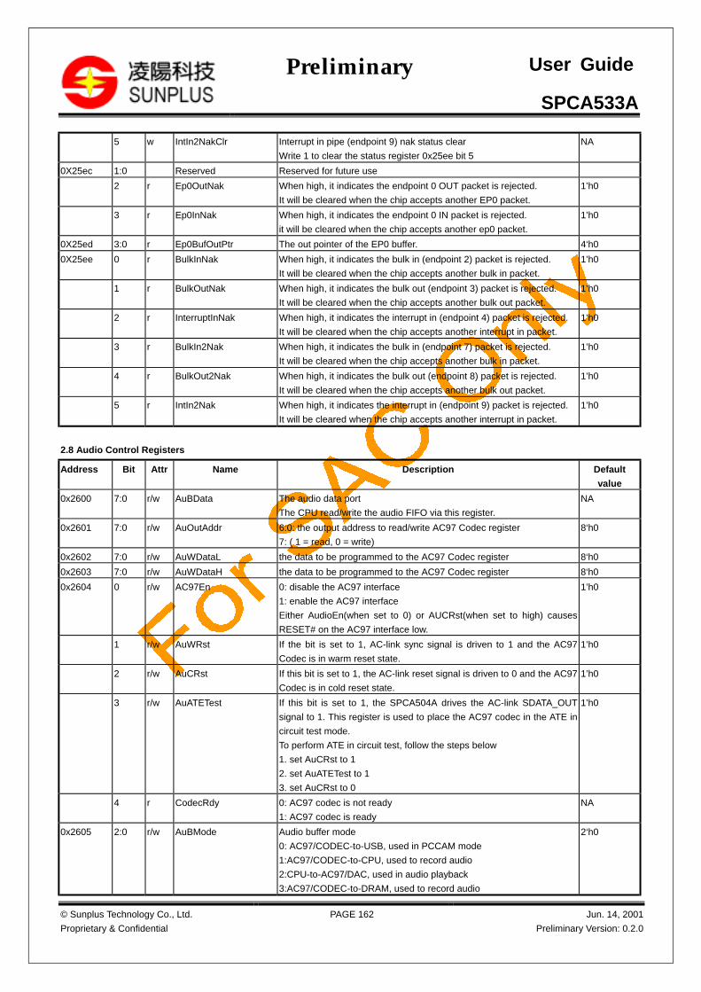
SPCA533A
© Sunplus Technology Co., Ltd.
Proprietary & Confidential
PAGE 162 Jun. 14, 2001
Preliminary Version: 0.2.0
Preliminary User Guide
5 w IntIn2NakClr Interrupt in pipe (endpoint 9) nak status clear
Write 1 to clear the status register 0x25ee bit 5
NA
0X25ec 1:0 Reserved Reserved for future use
2 r Ep0OutNak When high, it indicates the endpoint 0 OUT packet is rejected.
It will be cleared when the chip accepts another EP0 packet.
1’h0
3 r Ep0InNak When high, it indicates the endpoint 0 IN packet is rejected.
it will be cleared when the chip accepts another ep0 packet.
1’h0
0X25ed 3:0 r Ep0BufOutPtr The out pointer of the EP0 buffer. 4‘h0
0X25ee 0 r BulkInNak When high, it indicates the bulk in (endpoint 2) packet is rejected.
It will be cleared when the chip accepts another bulk in packet.
1’h0
1 r BulkOutNak When high, it indicates the bulk out (endpoint 3) packet is rejected.
It will be cleared when the chip accepts another bulk out packet.
1’h0
2 r InterruptInNak When high, it indicates the interrupt in (endpoint 4) packet is rejected.
It will be cleared when the chip accepts another interrupt in packet.
1’h0
3 r BulkIn2Nak When high, it indicates the bulk in (endpoint 7) packet is rejected.
It will be cleared when the chip accepts another bulk in packet.
1’h0
4 r BulkOut2Nak When high, it indicates the bulk out (endpoint 8) packet is rejected.
It will be cleared when the chip accepts another bulk out packet.
1’h0
5 r IntIn2Nak When high, it indicates the interrupt in (endpoint 9) packet is rejected.
It will be cleared when the chip accepts another interrupt in packet.
1’h0
2.8 Audio Control Registers
Address Bit Attr Name Description Default
value
0x2600 7:0 r/w AuBData The audio data port
The CPU read/write the audio FIFO via this register.
NA
0x2601 7:0 r/w AuOutAddr 6:0: the output address to read/write AC97 Codec register
7: ( 1 = read, 0 = write)
8‘h0
0x2602 7:0 r/w AuWDataL the data to be programmed to the AC97 Codec register 8‘h0
0x2603 7:0 r/w AuWDataH the data to be programmed to the AC97 Codec register 8‘h0
0x2604 0 r/w AC97En 0: disable the AC97 interface
1: enable the AC97 interface
Either AudioEn(when set to 0) or AUCRst(when set to high) causes
RESET# on the AC97 interface low.
1’h0
1 r/w AuWRst If the bit is set to 1, AC-link sync signal is driven to 1 and the AC97
Codec is in warm reset state.
1’h0
2 r/w AuCRst If this bit is set to 1, the AC-link reset signal is driven to 0 and the AC97
Codec is in cold reset state.
1’h0
3 r/w AuATETest If this bit is set to 1, the SPCA504A drives the AC-link SDATA_OUT
signal to 1. This register is used to place the AC97 codec in the ATE in
circuit test mode.
To perform ATE in circuit test, follow the steps below
1. set AuCRst to 1
2. set AuATETest to 1
3. set AuCRst to 0
1’h0
4 r CodecRdy 0: AC97 codec is not ready
1: AC97 codec is ready
NA
0x2605 2:0 r/w AuBMode Audio buffer mode
0: AC97/CODEC-to-USB, used in PCCAM mode
1:AC97/CODEC-to-CPU, used to record audio
2:CPU-to-AC97/DAC, used in audio playback
3:AC97/CODEC-to-DRAM, used to record audio
2‘h0

SPCA533A
© Sunplus Technology Co., Ltd.
Proprietary & Confidential
PAGE 163 Jun. 14, 2001
Preliminary Version: 0.2.0
Preliminary User Guide
4:DRAM-to-AC97/DAC, used in audio playback
5:AC97/CODEC-to-DMAC, used to record audio
6:DMAC-to-AC97/DAC, used in audio playback
0x2606 0 r/w AuStereo AC97/Codec link audio data capture option
0: capture only the left channel audio data
1: capture both left and right channel audio data.
1’h0
1 r/w Au16bit AC97/Codec link audio data capture option
0: 8 bits per audio sample (MSB)
1: 16 bits per audio sample
the data is 2‘s complement values. Note that for the embedded audio
codec, 16-bit mode means appending 8 bits "0" to the LSB
1’h0
2 r/w PCM8En AC97/Codec PCM8 format
0: the audio data format is defined in bit 3
1: use PCM8 format, which is 8 bits per sample and the data range is
from 0 to 255.
PCM8En can be set to 1 only in the audio playback mode
1’h0
3 reserved Reserved
5:4 r/w AuDSMode AC97/Codec audio data capture option. This feature is design to
conserve the space of the storage media when the SPCA504A records
the audio data via the AC-link.
0: no down sample
1: 2 times down sample
2: 6 times down sample
please set AuDSMode 0 when playing back
2‘h0
0x2607 2:0 r/w AuDFreq Data to AC97 codec (audio playback)
frequency
0: 48 KHz
1: 24 KHz
4: 8 KHz
please set AuDSMode 0 when playing back
3‘h0
0x2608 8:0 r/w AuBLThrL Audio FIFO low threshhold (low byte).
During operation, the CPU may get the audio buffer status by reading
the data count in register 0x26b5 and 0x26b4, or sets the threshold of
the data count ,then wait for the interrupt. The CPU will be interrupted
when the amount of data in the audio FIFO is less then the low
threshold.
8‘h0
0x2609 0 r/w AuBLThrH Audio FIFO low threshold(high byte).
During operation, the CPU may get the audio buffer status by reading
the data count in register 0x26b5 and 0x26b4, or sets the threshold of
the data count ,then wait for the interrupt. The CPU will be interrupted
when the amount of data in the audio FIFO is less then the low
threshold.
1‘h0
0x260a 7:0 r/w AuBHThrL Audio FIFO high threshold (low byte).
In the other way, the CPU will be interrupted when the amount of data in
the audio FIFO exceeds the one defined in AuBHThr.
8‘h0
0x260b 7:0 r/w AuBHThrH Audio FIFO high threshold (high byte).
In the other way, the CPU will be interrupted when the amount of data in
the audio FIFO exceeds the one defined in AuBHThr.
1‘h0
0x2660 7:0 r/w MPTxDataL MP3 processor serial interface TX data word (low byte). 8‘h0
0x2661 7:0 r/w MPTxDataH MP3 processor serial interface TX data word (high byte). Each time
when this byte is written, the data(in word) is transferred to the MP3
processor. Writing to this register will trigger a TX cycle to the MP3
8‘h0

SPCA533A
© Sunplus Technology Co., Ltd.
Proprietary & Confidential
PAGE 164 Jun. 14, 2001
Preliminary Version: 0.2.0
Preliminary User Guide
processor.
0x2662 7:0 r MPRxDataL MP3 processor serial interface RX data word (low byte). NA
0x2663 7:0 r MPRxDataH MP3 processor serial interface RX data word (high byte). Reading this
register will trigger the next RX cycle from the MP3 processor.
NA
0x2664 0 r/w MP3en MP3 processor interface enable bit
0: disable the serial interface to MP3 processor
1: enable the serial interface to MP3 processor
1’h0
0x2665 0 r/w MPSIwrnn Data transfer direction
0: data from MP3 processor to the camera ASIC
1: data from the camera ASIC to the MP3 processor
1’h0
0x2666 1:0 r/w MPSIfreq[1:0] MP3 processor serial interface, serial clock frequency selection
0: 1.5 MHz
1: 3 MHz
2: 6 MHz
2‘b0
0x2667 7:0 r/w MplengthL MP3 processor interface, data transfer length (low byte).
This register combined with MplengthH indicates how many words is
going to be sent/received from the MP3 processor.
8‘h0
0x2668 1:0 r/w MplengthH MP3 processor interface, data transfer length.
This register combined with MplengthL indicates how many words is
going to be sent/received from the MP3 processor.
2‘b0
0x2669 0 r MPSIready During a TX cycle, MPSIready indicates the data has been transferred
to the MP3 processor, the CPU may write the next data.
During an RX cycle, MPSIready indicates a word of data is received
from the MP3 processor, the CPU may read the data from register
0x2662 and 0x2663.
1’h0
1 r MPFCEB1 MP3 processor flag, this flag indicates whether the processor is ready. NA
2 r MPFCEB2 MP3 processor flag, this flag is a periodical clock for record time stamp. NA
0x266a 0 w MPprefetch Write 1 to pre-fetch a word of data from the MP3 processor NA
1 w MPSIdummy Write 1 to output 8 dummy clocks NA
0x266b 0 r/w MPrstnn reset signal for the MP3 processor (active low) 1’h1
0x2670 0 r/w ADCceb ADC chip enable bit(low active)
Write 0 to enable ADC
Write 1 to disable ADC
Please enable ADCceb, ADCshe, ADCagce, and ADCcade all together
when using ADC
1’h1
1 r/w ADCade ADC ad enable
Write 1 to enable ADC ad
Write 0 to disable ADC ad
1’h0
2 r/w ADCagce ADC auto gain control enable
Write 1 to enable ADC auto gain control
Write 0 to disable ADC auto gain control
1’h0
3 r/w ADCshe ADC sample and hold enable
Write 1 to enable ADC sample and hold
Write 0 to disable ADC sample and hold
1’h0
0x2671 0 r/w ADCMute ADC Mute control
Write 1 to mute the ADC input
Write 0 to unmute the ADC input
1’h1
0x2674 1:0 r/w CodecFrqSel 0: 48KHz
1: 24KHz
2: 8KHz
3: 44.1KHz
4’h0
0x2675 0 r/w DACEn 0: DAC disable 1’h0

SPCA533A
© Sunplus Technology Co., Ltd.
Proprietary & Confidential
PAGE 165 Jun. 14, 2001
Preliminary Version: 0.2.0
Preliminary User Guide
1: DAC enable
1 r/w DACInvOut 0: Signed data for DAC
1: Unsigned data for DAC
1’b0
0x2676 7:0 r/w EmbDACVolume Volume control for the embedded audio DAC
0: mute
1: default setting
2~255: audio pcm value * EmbDACVolume
8’h1
0x2680 0 r/w ADPCMEncEn Write 1 to enable the ADPCM encoder 1’h0
1 r/w ADPCMDecEn Write 1 to enable the ADPCM decoder 1’h0
0x2681 0 r/w ADPCMPageMode 0: 512 bytes per page
1: 256 bytes per page
1’h0
0x26a0 0 w AuOutReg When write one, the value in the output address and data (only for the
write mode) will be transmitted in the next audio frame. Do write one
again when another data needs to be transmitted to the AC97 register.
NA
1 w AuBClr When write one, all status about the audio buffer will be cleared. Do
write one again when the audio needs to be cleared.
NA
0x26b0 6:0 r AuInAddr the register address in audio input frame 7‘h0
0x26b1 7:0 r AuInDataL The register data(low byte) in audio input frame 8‘h0
0x26b2 7:0 r AuInDataH The register data(high byte) in audio input frame 8‘h0
0x26b3 0 r AuOutBsy When high, it indicates the process to out audio register is still going. 1’h0
1 r/w AuInVld When high, it indicates there is valid data in the audio input address and
data registers and the following input register data will be skipped.
When write zero, the bit will be cleared.
1’h0
0x26b4 7:0 r AuBCntL The count of available data(low byte) in the audio buffer 8‘h0
0x26b5 7:0 r AuBCntH The count of available data(high byte) in the audio buffer 8‘h0
0x26c0 0 r/w AuBUnLThr When high, it indicates the audio buffer count is just under the low
threshold.
When write zero, the event will be cleared.
1’h0
1 r/w AuBOvHThr When high, it indicates the audio buffer count is just over the high
threshold.
When write zero, the event will be cleared.
1’h0
0x26c1 0 R MP3int MP3 processor interrupt, the interrupt is generated when MPFCEB goes
from low to high.
1’h0
0x26d0 0 r/w AuBUnLThrEn When high, it indicates the interrupt event for audio buffer count just
under the low threshold is enabled.
1’h0
1 r/w AuBOvHThrEn When high, it indicates the interrupt event for audio buffer count just
over the high threshold is enabled.
1’h0
0x26d1 0 r/w MP3inten MP3 processor interrupt enable bit
0: disable , 1: enable
1’h0
2.9 SDRAM Control Registers
Address bit Attr Name Description Default
value
0X2700 7:0 r/w DRAMdata[7:0] DRAM data port low byte 8’b0
0X2701 7:0 r/w DRAMdata[15:8] DRAM data port high byte 8’b0
0X2702 7:0 r/w DRAMaddr[7:0] DRAM access address bit [7:0] 8’b0
0X2703 7:0 r/w DRAMaddr[15:8] DRAM access address bit [15:8] 8’b0
0X2704 7:0 r/w DRAMaddr[23:16] DRAM access address bit [23:16] 86b0
0X2705 7:0 rw CLRsize[7:0] During clear DRAM operation, this register indicates how many
words will be cleared. The maximum size of each Clear DRAM
operation is 64K words.
8’b0

SPCA533A
© Sunplus Technology Co., Ltd.
Proprietary & Confidential
PAGE 166 Jun. 14, 2001
Preliminary Version: 0.2.0
Preliminary User Guide
0X2706 7:0 rw CLRsize[15:8] 8’b0
0X2707 1:0 rw DRAMtype[1:0] DRAM type selection
0: SDRAM 1Mx16 bits x1
1: SDRAM 4Mx16 bits,4-bank
2: SDRAM 8M x 16 bits , 4-bank
3: SDRAM 16M x 16 bits, 4-bank
2’b0
2 rw Casmode SDRAM casnn control signal type selection
0: only asserted during the first clock of access
1: assert for every access clock. This allows the DRAM controller to
change the column address jumping sequence during a burst
access. It is used when the horizontal sub-sampling of TV display is
applied.
1’b0
0X2708 0 rw Srefresh 0: normal operation
1: force SDRAM into self refresh state
1’b0
0X2709 3:0 rw SDCKphase[3:0] SDRAM clock phase adjustment. Each step is 1.3 ns , bit[3] reverse
the clock
4’b0
4 rw sdckmode 0:stop the sdram clock while in the idle mode
1:always output the sdram clock
1’b0
0X270a 6:0 rw Refrate[6:0] DRAM refresh rate.
The DRAM refresh is based on the Horizontal sync signal. The
sdram will perform refrate[6:0] times of refresh cycles for a
Horizontal sync signal.
7’d7
0X270b 7:0 rw ClrData[7:0] The value to filled into the DRAM when the clear DRAM operation
is performed.
8’b0
0X270c 7:0 rw ClrData[15:8] 8’b0
0X270e 2:0 rw Imgtype[2:0] 3’b000: raw data
3’b001: YUV422 Non-compression
3’b010: YUV422 compression
3’b011: YUV420, Non-compression
3’b100: reserved
3’b101: YUV420, compression
3’b110: reserved
3’b111: reserved
3’b0
0X270f 1:0 rw Fieldmode[1:0] Image input mode selection
0: single field input.
1: reserved
2: 2-field mode, for interlace CCD
3: Special 2-field mode, for Sharp LZ23J3V
In PCCAM mode, this register must always be set to 0. If an
interlace CCD is connected to the SPCA533, then the sensor must
be operated in the monitor (filed-accumulation) mode. If a TV
decoder is connected to the SPCA533, then every filed is regarded
as a complete image.
In DSC mode, this register is set to 2 or 3 to get a full image of two
fields. Set this register to 2 when SPCA503 is connected to a TV
decoder.
2’b0
0X2711 0 rw tmbformat The DRAMCTRL will put the DCT DC value to the SDRAM. The
“tmbformat” will determine the format that the DC value is arranged
in the SDRAM.
0: in the order that the JPEG output the DC to the DRAMCTRL, that
is the YYUV format.
1: in the order that the frame buffer arrange the YUV data, that is
1’b0

SPCA533A
© Sunplus Technology Co., Ltd.
Proprietary & Confidential
PAGE 167 Jun. 14, 2001
Preliminary Version: 0.2.0
Preliminary User Guide
the YUYV format.
0X2712 0 rw DoCDSP This bit is used if a interlaced-type CCD is connected to the
SPCA503. It must be set to 1 before starting the CDSP processing
of the image. In other operation it must be set to 0.
1’b0
0X2713 0 rw lcdpbmode 0: The LCD displayed data address is calculated from the LCD
module.
1: The LCD displayed data address is calculated from the
DRAMCTRL module.
1’b0
0X2715 0 rw vlcardy Status bit for the video clip buffer A.
If the entire clipped frame is in buffer A, the hardware will set this bit
to 1. Then the firmware can perform DMA to get the image data.
After that, the firmware must reset this bit to 0 to allow another
image coming.
1’b0
0X2716 0 rw Vlcbrdy Status bit for the video clip buffer B.
If the entire clipped frame is in buffer B, the hardware will set this bit
to 1. Then the firmware can perform DMA to get the image data.
After that, the firmware must reset this bit to 0 to allow another
image coming.
1’b0
0X2717 0 rw refsrc SDRAM refresh source
0: generate the refresh cycle from the TG h-sync signal
1: generate the refresh cycle from the LCD h-sync signal
1’b0
0X2720 7:0 rw Size[7:0] During compression, the size record the final size of the
compressed image.
During playback (decompress), the size register must filled with the
size of the VLC data before moving data from flash memoty to the
DARM VLC FIFO.
8’b0
0X2721 7:0 rw Size[15:8] 8’b0
0X2722 7:0 rw Size[23:16] 8’b0
0X2723 2:0 rw Audbufsize[2:0] The allocation size of the audio buffer in SDRAM
0: 1K bytes
1: 2K bytes
2: 4K bytes
3: 8K bytes
4: 128 bytes(for testing)
3’b0
0X2730 7:0 rw VLCstart[7:0] The starting address of the VLC FIFO. 8’b0
0X2731 7:0 rw VLCstart[15:8] 8’b0
0X2732 7:0 rw VLCstart[23:16] 8’b0
0X2733 7:0 rw VLCBstart[7:0] The starting address of the VLCB FIFO. 8’b0
0X2734 7:0 rw VLCBstart[15:8] 8’b0
0X2735 7:0 rw VLCBstart[23:16] 8’b0
0X2736 7:0 rw TMBstart[7:0] Define the Thumbnail buffer starting address. 8’b0
0X2737 7:0 rw TMBstart[7:0] 8’b0
0X2738 7:0 rw TMBstart[23:16] 8’b0
0X2739 7:0 rw CAPint[7:0] Image capture interval. The DRAMCTRL will get one frame out of
every “capint” input frames
8’b0
0X273A 7:0 rw AUDstaddr[7:0] The starting address of audio FIFO 8’b0
0X273B 7:0 rw AUDstaddr[15:8] 8’b0
0X273C 7:0 rw AUDstaddr[23:16] 8’b0
0X273D 0 rw Audiodma Indicates the DRAM DMA is for the audio FIFO. This bit must be
asserted before triggering the audio dma to SDRAM.
1’b0
0X273E 0 rw Audclipen Actives the audio clip function 1’b0
1 rw Auddir The audio data path direction 1’b0

SPCA533A
© Sunplus Technology Co., Ltd.
Proprietary & Confidential
PAGE 168 Jun. 14, 2001
Preliminary Version: 0.2.0
Preliminary User Guide
0: from sdram to audio block
1: from audio block to sdram
0X2744 0 rw Bwmode 0: Color moode
1:Black and white mode
1’b0
1 rw Raw8bit 0:10-bit raw data
1: 8-bit raw data
1’b0
0X2745 2:0 rw Pbrescale[2:0] Scaling of the image in the playback mode.
0: full size playback
1: 1/8 size playback
2: 2/8 size playback
3: 3/8 size playback
4: 4/8 size playback
5: 5/8 size playback
6: 6/8 size playback
7: 7/8 size playback
3’b0
0X2746 0 rw Frcen Frame rate concersion enable
0: disable frame rate conversion
1: enable frame rate conversion
1’b0
0X2747 0 rw Frcmode Frame rate conversion mode
0: CCD is faster than LCD display
1: CCD is slower than LCD display
1’b0
0X2748 0 rw Lcdsrcidx LCD frame buffer display index
0: Frame buffer A
1: Frame bugger B
1’b0
0X2749 0 rw Ccdsrcidx CCD frame buffer write index
0: Frame buffer A
1: Frame bugger B
1’b0
0X274A 0 rw Jpgsrcidx JPEG source frame buffer index
0: Frame buffer A
1: Frame bugger B
1’b0
0X2750 7:0 Rw Dmastaddr[7:0] The DMAstaddr[23:0] indicates the starting address that the dma
controller will access DRAM.
8’b0
0X2751 7:0 Rw Dmastaddr[15:8] 8’b0
0X2752 7:0 Rw Dmastaddr[23:16] 8’b0
0X2753 7:0 rw Afbaddr[7:0] Fram buffer A starting address low byte 8’b0
0X2754 7:0 rw Afbaddr[15:8] Fram buffer A starting address middle byte 8’b0
0X2755 7:0 rw Afbaddr[23:16] Fram buffer A starting address high byte 8’b0
0X2756 7:0 rw Bfbaddr[7:0] Fram buffer B starting address low byte 8’b0
0X2757 7:0 rw Bfbaddr[15:8] Fram buffer B starting address middle byte 8’b0
0X2758 7:0 rw Bfbaddr[23:16] Fram buffer B starting address high byte 8’b0
0X2759 7:0 rw osdaddr[7:0] Osd buffer starting address low byte 8’b0
0X275A 7:0 rw osdaddr[15:8] Osd buffer starting address middle byte 8’b0
0X275B 7:0 rw osdaddr[23:16] Osd buffer starting address high byte 8’b0
0X2760 7:0 rw Afbhsize[7:0] Frame buffer A image width low byte 8’b0
0X2761 3:0 rw Afbhsize[11:8] Frame buffer A image width high byte 8’b0
0X2762 7:0 rw Afvhsize[7:0] Frame buffer A image height low byte 8’b0
0X2763 3:0 rw Afvhsize[11:8] Frame buffer A image height high byte 8’b0
0X2764 7:0 rw Bfbhsize[7:0] Frame buffer B image width low byte 8’b0
0X2765 3:0 rw Bfbhsize[11:8] Frame buffer B image width high byte 8’b0
0X2766 7:0 rw Bfbvsize[7:0] Frame buffer B image height low byte 8’b0
0X2767 3:0 rw Bfbvsize[11:8] Frame buffer B image height high byte 8’b0
0X2768 7:0 rw Rfbaddr[7:0] Raw data frame buffer starting address low byte 8’b0
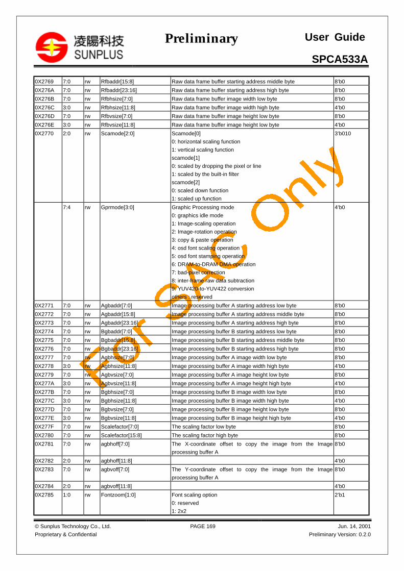
SPCA533A
© Sunplus Technology Co., Ltd.
Proprietary & Confidential
PAGE 169 Jun. 14, 2001
Preliminary Version: 0.2.0
Preliminary User Guide
0X2769 7:0 rw Rfbaddr[15:8] Raw data frame buffer starting address middle byte 8’b0
0X276A 7:0 rw Rfbaddr[23:16] Raw data frame buffer starting address high byte 8’b0
0X276B 7:0 rw Rfbhsize[7:0] Raw data frame buffer image width low byte 8’b0
0X276C 3:0 rw Rfbhsize[11:8] Raw data frame buffer image width high byte 4’b0
0X276D 7:0 rw Rfbvsize[7:0] Raw data frame buffer image height low byte 8’b0
0X276E 3:0 rw Rfbvsize[11:8] Raw data frame buffer image height low byte 4’b0
0X2770 2:0 rw Scamode[2:0] Scamode[0]
0: horizontal scaling function
1: vertical scaling function
scamode[1]
0: scaled by dropping the pixel or line
1: scaled by the built-in filter
scamode[2]
0: scaled down function
1: scaled up function
3’b010
7:4 rw Gprmode[3:0] Graphic Processing mode
0: graphics idle mode
1: Image-scaling operation
2: Image-rotation operation
3: copy & paste operation
4: osd font scaling operation
5: osd font stamping operation
6: DRAM-to-DRAM DMA operation
7: bad-pixel correction
8: inter-frame raw data subtraction
9: YUV420-to-YUV422 conversion
others : reserved
4’b0
0X2771 7:0 rw Agbaddr[7:0] Image processing buffer A starting address low byte 8’b0
0X2772 7:0 rw Agbaddr[15:8] Image processing buffer A starting address middle byte 8’b0
0X2773 7:0 rw Agbaddr[23:16] Image processing buffer A starting address high byte 8’b0
0X2774 7:0 rw Bgbaddr[7:0] Image processing buffer B starting address low byte 8’b0
0X2775 7:0 rw Bgbaddr[15:8] Image processing buffer B starting address middle byte 8’b0
0X2776 7:0 rw Bgbaddr[23:16] Image processing buffer B starting address high byte 8’b0
0X2777 7:0 rw Agbhsize[7:0] Image processing buffer A image width low byte 8’b0
0X2778 3:0 rw Agbhsize[11:8] Image processing buffer A image width high byte 4’b0
0X2779 7:0 rw Agbvsize[7:0] Image processing buffer A image height low byte 8’b0
0X277A 3:0 rw Agbvsize[11:8] Image processing buffer A image height high byte 4’b0
0X277B 7:0 rw Bgbhsize[7:0] Image processing buffer B image width low byte 8’b0
0X277C 3:0 rw Bgbhsize[11:8] Image processing buffer B image width high byte 4’b0
0X277D 7:0 rw Bgbvsize[7:0] Image processing buffer B image height low byte 8’b0
0X277E 3:0 rw Bgbvsize[11:8] Image processing buffer B image height high byte 4’b0
0X277F 7:0 rw Scalefactor[7:0] The scaling factor low byte 8’b0
0X2780 7:0 rw Scalefactor[15:8] The scaling factor high byte 8’b0
0X2781 7:0 rw agbhoff[7:0] The X-coordinate offset to copy the image from the Image
processing buffer A
8’b0
0X2782 2:0 rw agbhoff[11:8] 4’b0
0X2783 7:0 rw agbvoff[7:0] The Y-coordinate offset to copy the image from the Image
processing buffer A
8’b0
0X2784 2:0 rw agbvoff[11:8] 4’b0
0X2785 1:0 rw Fontzoom[1:0] Font scaling option
0: reserved
1: 2x2
2’b1
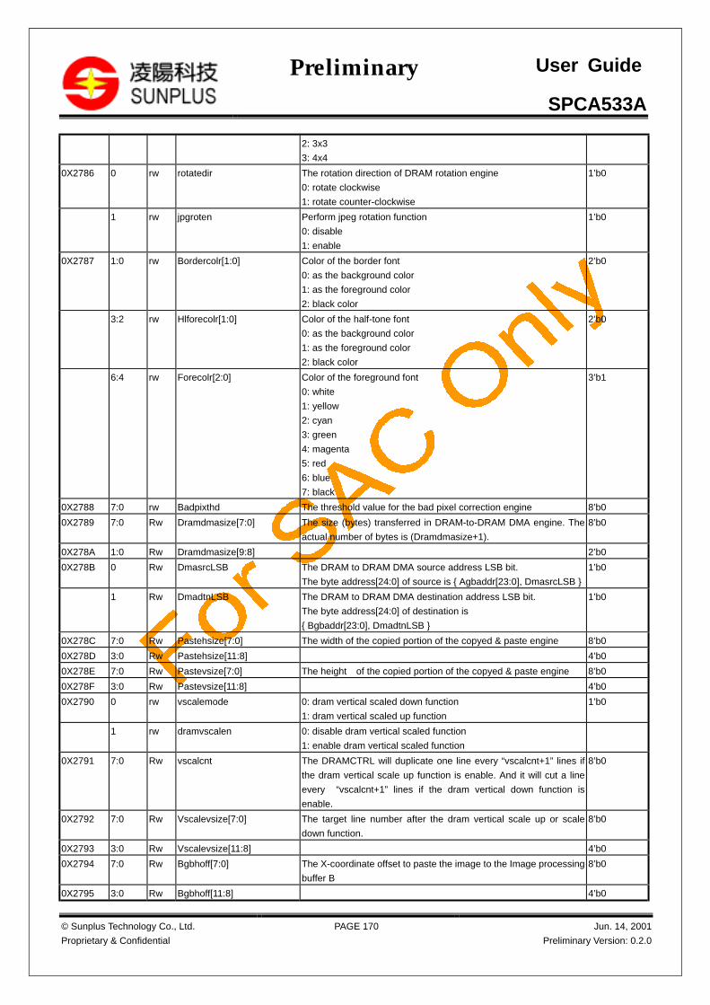
SPCA533A
© Sunplus Technology Co., Ltd.
Proprietary & Confidential
PAGE 170 Jun. 14, 2001
Preliminary Version: 0.2.0
Preliminary User Guide
2: 3x3
3: 4x4
0X2786 0 rw rotatedir The rotation direction of DRAM rotation engine
0: rotate clockwise
1: rotate counter-clockwise
1’b0
1 rw jpgroten Perform jpeg rotation function
0: disable
1: enable
1’b0
0X2787 1:0 rw Bordercolr[1:0] Color of the border font
0: as the background color
1: as the foreground color
2: black color
2’b0
3:2 rw Hlforecolr[1:0] Color of the half-tone font
0: as the background color
1: as the foreground color
2: black color
2’b0
6:4 rw Forecolr[2:0] Color of the foreground font
0: white
1: yellow
2: cyan
3: green
4: magenta
5: red
6: blue
7: black
3’b1
0X2788 7:0 rw Badpixthd The threshold value for the bad pixel correction engine 8’b0
0X2789 7:0 Rw Dramdmasize[7:0] The size (bytes) transferred in DRAM-to-DRAM DMA engine. The
actual number of bytes is (Dramdmasize+1).
8’b0
0X278A 1:0 Rw Dramdmasize[9:8] 2’b0
0X278B 0 Rw DmasrcLSB The DRAM to DRAM DMA source address LSB bit.
The byte address[24:0] of source is { Agbaddr[23:0], DmasrcLSB }
1’b0
1 Rw DmadtnLSB The DRAM to DRAM DMA destination address LSB bit.
The byte address[24:0] of destination is
{ Bgbaddr[23:0], DmadtnLSB }
1’b0
0X278C 7:0 Rw Pastehsize[7:0] The width of the copied portion of the copyed & paste engine 8’b0
0X278D 3:0 Rw Pastehsize[11:8] 4’b0
0X278E 7:0 Rw Pastevsize[7:0] The height of the copied portion of the copyed & paste engine 8’b0
0X278F 3:0 Rw Pastevsize[11:8] 4’b0
0X2790 0 rw vscalemode 0: dram vertical scaled down function
1: dram vertical scaled up function
1’b0
1 rw dramvscalen 0: disable dram vertical scaled function
1: enable dram vertical scaled function
0X2791 7:0 Rw vscalcnt The DRAMCTRL will duplicate one line every “vscalcnt+1” lines if
the dram vertical scale up function is enable. And it will cut a line
every “vscalcnt+1” lines if the dram vertical down function is
enable.
8’b0
0X2792 7:0 Rw Vscalevsize[7:0] The target line number after the dram vertical scale up or scale
down function.
8’b0
0X2793 3:0 Rw Vscalevsize[11:8] 4’b0
0X2794 7:0 Rw Bgbhoff[7:0] The X-coordinate offset to paste the image to the Image processing
buffer B
8’b0
0X2795 3:0 Rw Bgbhoff[11:8] 4’b0
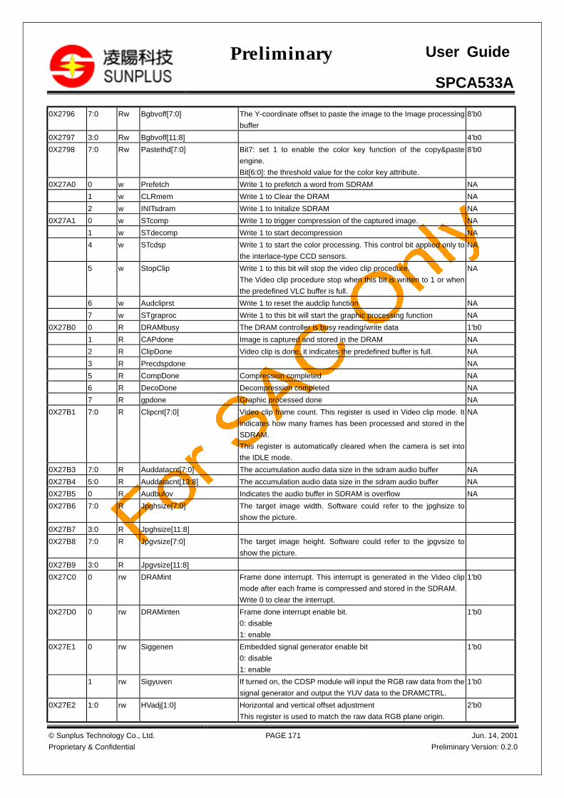
SPCA533A
© Sunplus Technology Co., Ltd.
Proprietary & Confidential
PAGE 171 Jun. 14, 2001
Preliminary Version: 0.2.0
Preliminary User Guide
0X2796 7:0 Rw Bgbvoff[7:0] The Y-coordinate offset to paste the image to the Image processing
buffer
8’b0
0X2797 3:0 Rw Bgbvoff[11:8] 4’b0
0X2798 7:0 Rw Pastethd[7:0] Bit7: set 1 to enable the color key function of the copy&paste
engine.
Bit[6:0]: the threshold value for the color key attribute.
8’b0
0X27A0 0 w Prefetch Write 1 to prefetch a word from SDRAM NA
1 w CLRmem Write 1 to Clear the DRAM NA
2 w INITsdram Write 1 to Initalize SDRAM NA
0X27A1 0 w STcomp Write 1 to trigger compression of the captured image. NA
1 w STdecomp Write 1 to start decompression NA
4 w STcdsp Write 1 to start the color processing. This control bit applied only to
the interlace-type CCD sensors.
NA
5 w StopClip Write 1 to this bit will stop the video clip procedure.
The Video clip procedure stop when this bit is written to 1 or when
the predefined VLC buffer is full.
NA
6 w Audcliprst Write 1 to reset the audclip function NA
7 w STgraproc Write 1 to this bit will start the graphic processing function NA
0X27B0 0 R DRAMbusy The DRAM controller is busy reading/write data 1’b0
1 R CAPdone Image is captured and stored in the DRAM NA
2 R ClipDone Video clip is done, it indicates the predefined buffer is full. NA
3 R Precdspdone NA
5 R CompDone Compression completed NA
6 R DecoDone Decompression completed NA
7 R gpdone Graphic processed done NA
0X27B1 7:0 R Clipcnt[7:0] Video clip frame count. This register is used in Video clip mode. It
indicates how many frames has been processed and stored in the
SDRAM.
This register is automatically cleared when the camera is set into
the IDLE mode.
NA
0X27B3 7:0 R Auddatacnt[7:0] The accumulation audio data size in the sdram audio buffer NA
0X27B4 5:0 R Auddatacnt[13:8] The accumulation audio data size in the sdram audio buffer NA
0X27B5 0 R Audbufov Indicates the audio buffer in SDRAM is overflow NA
0X27B6 7:0 R Jpghsize[7:0] The target image width. Software could refer to the jpghsize to
show the picture.
0X27B7 3:0 R Jpghsize[11:8]
0X27B8 7:0 R Jpgvsize[7:0] The target image height. Software could refer to the jpgvsize to
show the picture.
0X27B9 3:0 R Jpgvsize[11:8]
0X27C0 0 rw DRAMint Frame done interrupt. This interrupt is generated in the Video clip
mode after each frame is compressed and stored in the SDRAM.
Write 0 to clear the interrupt.
1’b0
0X27D0 0 rw DRAMinten Frame done interrupt enable bit.
0: disable
1: enable
1’b0
0X27E1 0 rw Siggenen Embedded signal generator enable bit
0: disable
1: enable
1’b0
1 rw Sigyuven If turned on, the CDSP module will input the RGB raw data from the
signal generator and output the YUV data to the DRAMCTRL.
1’b0
0X27E2 1:0 rw HVadj[1:0] Horizontal and vertical offset adjustment
This register is used to match the raw data RGB plane origin.
2’b0
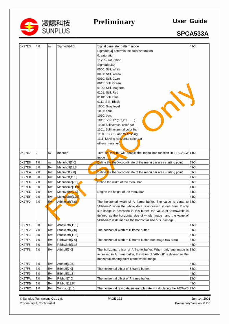
SPCA533A
© Sunplus Technology Co., Ltd.
Proprietary & Confidential
PAGE 172 Jun. 14, 2001
Preliminary Version: 0.2.0
Preliminary User Guide
0X27E3 4:0 rw Sigmode[4:0] Signal generator pattern mode
Sigmode[4] determin the color saturation
0: saturation
1: 75% saturation
Sigmode[3:0]
0000: Still, White
0001: Still, Yellow
0010: Still, Cyan
0011: Still, Green
0100: Still, Magenta
0101: Still, Red
0110: Still, Blue
0111: Still, Black
1000: Gray level
1001: hcnt
1010: vcnt
1011: hcnt-17 (0,1,2,3…….)
1100: Still vertical color bar
1101: Still horizontal color bar
1110: R, G, B, and W flashing
1111: Moving horizontal color bar
others : reserved
4’b0
0X27E7 0 rw menuen Turn on this bit will enable the menu bar function in PREVIEW
mode
1’b0
0X27E8 7:0 rw Menuhoff[7:0] Define the the X-coordinate of the menu bar area starting point 8’b0
0X27E9 3:0 Rw Menuhoff[11:8] 4’b0
0X27EA 7:0 Rw Menuvoff[7:0] Define the the Y-coordinate of the menu bar area starting point 8’b0
0X27EB 3:0 Rw Menuvoff[11:8] 4’b0
0X27EC 7:0 Rw Menuhsize[7:0] Define the width of the menu bar 8’b0
0X27ED 3:0 Rw Menuhsize[11:8] 4’b0
0X27EE 7:0 Rw Menuvsize[7:0] Degine the height of the menu bar 8’b0
0X27EF 3:0 Rw Menuvsize[11:8] 4’b0
0X27F0 7:0 Rw Afbhwidth[7:0] The horizontal width of A frame buffer. The value is equal to
“Afbhsize” when the whole data is accessed in one time. If only
sub-image is accessed in this buffer, the value of “Afbhwidth” is
defined as the horizontal size of whole image and the value of
“Afbhsize” is defined as the horizontal size of sub-image.
8’h0
0X27F1 3:0 Rw Afbhwidth[11:8] 4’h0
0X27F2 7:0 Rw Bfbhwidth[7:0] The horizontal width of B frame buffer. 8’h0
0X27F3 3:0 Rw Bfbhwidth[11:8] 4’h0
0X27F4 7:0 Rw Rfbhwidth[7:0] The horizontal width of R frame buffer. (for image raw data) 8’h0
0X27F5 3:0 Rw Rfbhwidth[11:8] 4’h0
0X27F6 7:0 Rw Afbhoff[7:0] The horizontal offset of A frame buffer. When only sub-image is
accessed in A frame buffer, the value of “Afbhoff” is defined as the
horizontal starting point of the whole image
8’h0
0X27F7 3:0 Rw Afbhoff[11:8] 4’h0
0X27F8 7:0 Rw Bfbhoff[7:0] The horizontal offset of B frame buffer. 8’h0
0X27F9 3:0 Rw Bfbhoff[11:8] 4’h0
0X27FA 7:0 Rw Rfbhoff[7:0] The horizontal offset of R frame buffer. 8’h0
0X27FB 3:0 Rw Rfbhoff[11:8] 4’h0
0X27FC 1:0 Rw Winhsub[1:0] The horizontal raw data subsample rate in calculating the AE/AWB 2’h0
SPCA533A
© Sunplus Technology Co., Ltd.
Proprietary & Confidential
PAGE 173 Jun. 14, 2001
Preliminary Version: 0.2.0
Preliminary User Guide
window value.
0: 1
1: 2
2: 4
3: 8
5:4 Rw Winvsub[1:0] The vertical raw data subsample rate in calculating the AE/AWB
window value.
0: 1
1: 2
2: 4
3: 8
2’h0
0X27FD 0 Rw winskipyuv The YUV data generated in calculating the AE/AWB window value:
0: store to SDRAM
1: skip
1’b0
1 rw cdsprawen The raw data generated by CDSP to store to SDRAM
0: disable
1: enable
1’b0
2 rw Frcimgfirst When one, force to indicate the current accessing part is the first
part of an image. The bit must be set when the offset of the first part
of accessing image doesn’t start from zero.
1’b0
3 rw Frcimglast When one, force to indicate the current accessing part is the last
part of an image. The bit must be set when the horzontal boundary
of the last part of accessing image doesn’t end in the horzintal
boundary of an image.
1’b0
2.10 JPEG Control Registers
Address Bit Attr Name DescriptionDefault
value
0X2800 7:0 r/w Yqtable Quantization table for Y-component
| The values of Q are filled in the raster-scan format.
0X283F 7:0 r/w
0X2840 7:0 r/w Cqtable Quantization table for C-component
|
0X287F 7:0 r/w
0X2880 7:0 r/w Noqtbl Index of the Q-table currently used
This register is for internal check only.
8’b0
0X2881 0 r/w Qvalueone 0: original
1: quantizer coefficients are set to one
1’b0
0X2882 0 r/w AccQtableEn 0: Normal operation (Q-table is not allowed to access)
1: Write 1 to this bit, Q-table (0x2800 – 0x287F) is accessible by CPU.
1’b0
0X2883 0 r/w Enthumb 1: Enable thumbbail image generation.
0: disable thumbnail image generation
Thumnail image is a by-producuct of the JPEG compression. The
SCPA533 extract the DC value of each JPEG MCU (minimum coding
unit) to construct the thumbail image. If the image type is raw data or
non-compression, then there is no thumbnial image available.
Note this bit is used in the DSC mode only. In the Video mode, this bit
should always be turned off.
1’b0
1 r/w StopEN 0: Normal operation.
1: Set this bit to enable stop mode. The decompression engine stops for
1’b0
SPCA533A
© Sunplus Technology Co., Ltd.
Proprietary & Confidential
PAGE 174 Jun. 14, 2001
Preliminary Version: 0.2.0
Preliminary User Guide
every block until the flag “blockend” is cleared (reg 0x2890 bit 0).
0X2884 0 r/w JFIF JFIF compatible bit.
0: Original
1: Compatiable with JFIF bit stream.
In a standard JFIF bit stream, 0XFF is used as a marker to indicated the
start point of a special control sequence. To represent VLC data 0XFF,
0X00 must be appended to distinguish from the marker.
1’b0
0X2885 0 r/w Truncated 0: Rounded after quantization
1: Truncated after quantization
1’b0
0X2886 2:0 r Vlcbit Indicates the number of stuffing 1’s in the last byte of the VLC stream.
0: non-stuffing 1’s
1: 1 stuffing 1.
……
7: 7 stuffing 1’s.
This information is passed to the PC in the Video mode for the software
decoding to double-check the JPEG VLC stream data integrity.
0X2887 0 r JFIFend After JFIF-compliant data is decompressed, check this bit to identify if
data stream is decompressed completely or not.
0: error happened.
1: decompressed completely.
NA
0X2888 7:0 r/w Restartmcu[7:0] If the vlc stream include MCU restart code, fill the restart MCU number.
Otherwise, set rstmcuno as 0 to disable restart code decompression.
8’b0
0X2889 7:0 r/w Restartmcu[15:8] 8’b0
0X2890 0 r/w Blockend In stop mode, active high after end of block. Write 0 to clear this flag. 1’b0
2.11 Serial Interface Control Registers
Address Bit Attr Name Description Default
value
0x2900 6:0 R/W Slaveaddr The Slave Address (the device address) 7’h0
0x2901 1:0 R/W Transmode Decide the serial transfer way2’b00: Synchronous Serial Normal mode2’b01: Synchronous Serial Burst mode2’b10: Using Three wire interface2’b11: Using Three wire interface by manual control
2’h0
5:4 R/W CDSmode This register determines different types of 'SEN', 'SDO', 'SCK' behavior
2'b00:
(1) Need no SEN signal. ONLY SCK, SDO
(2) Every rising SCK to latch SDO
(3) Last falling edge of SCK must latch SDO@HIGH
(4) After (3), a negedge@SDO will actually activate the programmed
data into internal registers,
EXAMPLE: SHARP IR3Y38M, 10-bit series data
2'b01:
(1) Need SCK, SDATA, SEN signals
(2) Every rising SCK to latch SDO
(3) Rising of SEN to actually activate the programmed data into internal
registers
EXAMPLE:
HITACHI HD49322F, 16-bit series data,
ADI AD9803, 14-bit series data,
EXAR XRD44L61/2, 10-bit series data
2’b00
SPCA533A
© Sunplus Technology Co., Ltd.
Proprietary & Confidential
PAGE 175 Jun. 14, 2001
Preliminary Version: 0.2.0
Preliminary User Guide
2'b10:
(1) Need SCK, SDATA, SEN signals
(2) Every rising SCK to latch DATA
(3) SEN stays LOW during SCK CLOCKING, then one PULSE, to actually
activate the programmed data into internal registers
EXAMPLE: PANASONIC AN2104FHQ, 11-bit series data
2’b11:
(1) Need SCK, SDO, SLOAD signals
(2) Every rising SCK to latch DATA
(3) SEN stays LOW during SCK CLOCKING
(4) At the end of transfer, need a SEN pulse
EXAMPLE: FUJITSU VGA Sensor
0x2902 0 R/W Subaddren Decide SUBADDR need or not in READ0: No sub address1: Has subaddress
1’b1
1 R/W Restarten This bit determines whether the Synchronous Serial interface’srepeat start condition. (Only work in Synchronous Serial interfaceread).0: Do not Repeat Start.1: Repeat Start.
1’b0
4 R/W Prefetch Writing this bit will initiate Synchronous Serial interface read sequence, it
will auto clear after BUSY signal go Low, then the user can read the data
buffer
1’b0
0x2903 0 R/W Syncvsync This bit determines whether the serial interface read/write willsynchronize with VSYNC falling edge or not.0: Read/write will occur immediately.1: Waiting the frontvd falling edge, then transfer.
1’b0
1 R/W Sifoe This bit determine the sen, sclk Pin output enable or not 1’b0
4 R/W Senpol SEN polarity select 1’b0
0x2904 2:0 R/W Freq Synchronous serial interface speed selection (Use in Synchronous Serial
interface)
3’b000: CPUCLK div 2048
3’b001: CPUCLK div 1024
3’b010: CPUCLK div 512
3’b011: CPUCLK div 256
3’b100: CPUCLK div 128
3’b101: CPUCLK div 64
3’b110: CPUCLK div 32
3’b111: CPUCLK div 16
3’b010
7:0 R/W Cntdiv The CPUCLK / CNT_DIV to generation the three wire clock (Used in CDS)
0x2905 3:0 R/W Wrcount Decide how many byte to write (Used in SSC mode)
4’h0: 16 Bytes
4’h1: 1 Bytes
.
.
4’hF: 15 Bytes
4’h1
7:4 R/W Rdcount Decide how many byte to read (Used in SSC mode) 4’h1
6:0 R/W Cdsbits The bits transfer to three wire interface (used in CDS mode) 7’h11
0x290A 0 R/W Msclk The serial interface sclk value, when Transmode = 2’b11 (manual enable) 1’b1
0x290B 0 R/W Msdo The serial interface sd value, when Transmode = 2’b11 (manual enable) 1’b1

SPCA533A
© Sunplus Technology Co., Ltd.
Proprietary & Confidential
PAGE 176 Jun. 14, 2001
Preliminary Version: 0.2.0
Preliminary User Guide
0x290C 0 R/W Msen The serial interface sen value, when Transmode = 2’b11 (manual enable) 1’b1
0x2910 7:0 R/W Addr0 The Address0 in BURST MODE (also the register address in normal
mode)
8’h0
0x2911 7:0 R/W Data0 The data buffer0 8’h0
0x2912 7:0 R/W Addr1 The BURST Address1 in BURST MODE 8’h0
0x2913 7:0 R/W Data1 The data buffer1 8’h0
0x2914 7:0 R/W Addr2 The BURST Address2 in BURST MODE 8’h0
0x2915 7:0 R/W Data2 The data buffer2 8’h0
0x2916 7:0 R/W Addr33 The BURST Address3 in BURST MODE 8’h0
0x2917 7:0 R/W Data3 The data buffer3 8’h0
0x2918 7:0 R/W Addr4 The BURST Address4 in BURST MODE 8’h0
0x2919 7:0 R/W Data 4 The data buffer4 8’h0
0x291A 7:0 R/W Addr 5 The BURST Address5 in BURST MODE 8’h0
0x291B 7:0 R/W Data 5 The data buffer5 8’h0
0x291C 7:0 R/W Addr 6 The BURST Address6 in BURST MODE 8’h0
0x291D 7:0 R/W Data 6 The data buffer6 8’h0
0x291E 7:0 R/W Addr 7 The BURST Address7 in BURST MODE 8’h0
0x291F 7:0 R/W Data 7 The data buffer7 8’h0
0x2910 7:0 R/W Addr 8 The BURST Address8 in BURST MODE 8’h0
0x2921 7:0 R/W Data 8 The data buffer8 8’h0
0x2922 7:0 R/W Addr 9 The BURST Address9 in BURST MODE 8’h0
0x2923 7:0 R/W Data 9 The data buffer9 8’h0
0x2924 7:0 R/W Addr 10 The BURST Address10 in BURST MODE 8’h0
0x2924 1:0 R/W thrfldmode The Field number of three field CCD 2’h0
4 R/W thrflden The Three field CCD enable 1’h0
5 R/W Inc3en The dram address control signal to CDSP 1’h0
7 R/W sony3field The SONY 3 Field CCD enable 1’h0
0x2925 7:0 R/W Data 10 The data buffer10 8’h0
0x2926 7:0 R/W Addr 11 The BURST Address11 in BURST MODE 8’h0
0x2926 1:0 R/W hoffsetmhi The Number of Pix clock for H-sync to Fronthdvalid when in monitor
mode, is the hoffsetm[11:10]
2’h0
0x2927 7:0 R/W Data 11 The data buffer11 8’h0
0x2928 7:0 R/W Addr 12 The BURST Address12 in BURST MODE 8’h0
0x2929 7:0 R/W Data 12 The data buffer12 8’h0
0x292A 7:0 R/W Addr 13 The BURST Address13 in BURST MODE 8’h0
0x292B 7:0 R/W Data 13 The data buffer13 8’h0
0x292C 7:0 R/W Addr 14 The BURST Address14 in BURST MODE 8’h0
0x292D 7:0 R/W Data 14 The data buffer14 8’h0
0x292E 7:0 R/W Addr 15 The BURST Address15 in BURST MODE 8’h0
0x292F 7:0 R/W Data 15 The data buffer15 8’h0
0x29A0 0 R Busy The status when Serial interface R/W register
1:Busy
0.Not Busy
NA
0x29B0 0 R/W Rstsif Write 1 to this bit will reset the serial interface 1’b0

SPCA533A
© Sunplus Technology Co., Ltd.
Proprietary & Confidential
PAGE 177 Jun. 14, 2001
Preliminary Version: 0.2.0
Preliminary User Guide
2.12 TV-IN / CMOS Sensor Control register
Address
Bit Attr Name Description Default
value
0x2A00 0 R/W Exthdipol The input H-sync polarity will be inverted when hi 1’b0
1 R/W Extvdipol The input H-sync polarity will be inverted when hi 1’b0
2 R/W Exthdopol The output V-sync polarity will be inverted when hi 1’b0
3 R/W Extvdopol The output V-sync polarity will be inverted when hi 1’b0
4 R/W Exthdoedge Decide output H-sync will work in Vclk positive edge or negativeedge0: Positive edge1: Negative edge
1’b0
0x2A01 1:0 R/W Nibborder Select the input order for nibble mode 2’b00
4 R/W Nibben Enable nibble data input0: Disable1: Enable
1’b0
0x2A02 0 R/W Tasc5130aen Enable Tasc5130a CMOS sensor for exposure control 1’b0
0x2A05 0 R/W Bt656en The 656 mode enable0: 601 mode1: 656 mode
1’b0
1 R/W Sub128en The Y, Cb, Cr, value will sub 128 when this bit set 1 1’b1
2 R/W Selfflden When in 601 mode, if the bit set to 1, then field signal will generateby it self
1’b0
4 R/W Tvreshhen This bit determinate the hvalid will set by Hoffset, or direct fromTvctr interface0: the signal direct from Tvctr interface1: You can set Hoffset, Hsize to get valid signal.
1’b0
5 R/W Tvreshven This bit determinate the vvalid will set by Voffset or direct fromTvctr interface0: the signal direct from Tvctr interface1: You can set Voffset, Vsize, to get valid signal.
1’b0
0x2A06 1:0 R/W Uvsel This will decide the first pixel is Cb, Cr, Y1or Y22’b00: Cb2’b01: Y12’b10: Cr2’b11: Y2
2’b00
4 R/W Fldpol 0: The Fld signal will not invert.1: The Fld signal will invert
1’b0
0x2A08, 07 15:0 R/W Flashwidth The Out put Flash control width 16’h60
0x2A09 2:0 R/W Flashmode 3’b000: The flash control output signal will out immediately.3’b001: The flash control output signal will sync with Sub inmonitor mode3’b010: The flash output signal will sync with sub in snap capturemode3’b011: The flash control output signal will sync with the line theuser define in Ftnum in monitor mode3’b100: The flash control output signal will sync with the line theuser define in Ftnum in snap capture mode
3’h0
3 R/W Flashpol Flash control polarity control 1’b0
4 R/W Flasgtrg When Set it, will trigger the flash function (flashen =1 & flashmode= 1), it will auto clear after control
1’b0
0x2A0B, 0A 11:0 R/W Ftnum The flash light will trigger in this line number define after Vd fallingedge when Flashmode = 2’b11
12’h60
SPCA533A
© Sunplus Technology Co., Ltd.
Proprietary & Confidential
PAGE 178 Jun. 14, 2001
Preliminary Version: 0.2.0
Preliminary User Guide
0x2A10 0 R/W Hreshen Enable reshape H-Sync to generation a new H-Sync signal toCDSP or others0: Disable1: Enable
1’b0
1 R/W Vreshen Enable reshape V-Sync to generation a new V-Sync signal toCDSP or others0: Disable1: Enable
1’b0
4 R/W Vreshcntclk Reshape V-sync counter clock select:0: H-sync1: vclk
1’b0
0x2A12, 11 11:0 R/W Hfall Control the position of internal H-sync falling edge, when H-syncreshape enable
12’h020
0x2A14, 13 11:0 R/W Hrise Control the position of internal H-sync rising edge, when H-syncreshape enable
12’h030
0x2A16, 15 11:0 R/W Vfall Control the position of internal V-sync falling edge, when V-syncreshape enable
12’h010
0x2A18, 17 11:0 R/W Vrise Control the position of internal V-sync rising edge, when V-syncreshape enable
12’h020
0x2A21, 20 11:0 R/W Hoffset [11:0] The Number of Pix clock for H-sync to Fronthdvalid in capturemode)
12’h29E
0x2A23, 22 11:0 R/W Voffset [11:0] The Number of H-sync for V-sync to frontvdvalid in CCD capturemode
12’h32
0x2A25, 24 11:0 R/W Hsize [11:0] The HSIZE of a frame in CCD capture mode 12’h640
0x2A27, 26 11:0 R/W Vsize [11:0] The VSIZE of a frame in CCD capture mode 12’h258
0x2A28 7:0 R/W Vdvalidpos [7:0] Define the Vdvalid rise and fall position after H-sync falling,(unitpixel clock)
8’h01
0x2A31, 30 9:0 R/W Hoffsetm The Number of Pix clock for H-sync to Fronthdvalid when inmonitor mode
12’h29E
0x2A33, 32 11:0 R/W Hsizem The HSIZE of a frame in monitor mode 12’h640
0x2A35, 34 9:0 R/W Voffsetm The Number of H-sync for V-sync to frontvdvalid in monitor mode 8’h03
0x2A37, 36 11:0 R/W Vsizem The VSIZE of a frame when in monitor mode 12’hF0
0x2A39, 38 9:0 R/W Voffsetafc The Number of H-sync for V-sync to frontvdvalid when CCDenable in AF capture mode mode
8’h60
0x2A3B, 3A 11:0 R/W Vsizeafc The VSIZE of a frame when CCD enable in AF capture mode 12’h100
0x2A3D, 3C 9:0 R/W Voffsetafm The Number of H-sync for V-sync to frontvdvalid when CCDenable in Af monitor mode mode
8’h10
0x2A3F, 3E 11:0 R/W Vsizeafm The VSIZE of a frame when CCD enable in AF monitor mode 12’h50
0x2A40 0 R/W Syncgenen Enable the sync generator module; means the CMOS sensor need to give
hd, vd.
0: Disable
1: Enable
1’b0
1 R/W Totalsvden When set, the Linetotal, Frametotal, Frametotalm,
Frametotalafc, Frametotalafm change will sync with frontvd fall edge
1’b0
4 R/W Frameblankcntclk Frame blank counter clock select:0: H-sync1: vclk
1’b0
0x2A42, 41 11:0 R/W Linetotal The Number of Pix clock in a line, to TG (also the value in capturemode)
12’h8E8
0x2A44, 43 9:0 R/W Lineblank The Number of Pix clock in H-sync blank, to TG (also the value incapture mode)
10’hE4
0x2A46, 45 11:0 R/W Frametotal The Number of H-sync in a frame to TG (also the value in capturemode)
12’h290
0x2A48, 47 9:0 R/W Frameblank The width of frame blank, the counter is base onH-sync when Frameblankcntclk = 0, else base on vclk (also the
10’h02

SPCA533A
© Sunplus Technology Co., Ltd.
Proprietary & Confidential
PAGE 179 Jun. 14, 2001
Preliminary Version: 0.2.0
Preliminary User Guide
value in capture mode)
0x2A4A, 49 10:0 R/W Hdvdopos This defines the exthdo and extvdo should separate how manypixels.
11’h1
0x2A51, 50 11:0 R/W Frametotalm The Number of H-sync in a frame, when CCD enable in monitormode
12’h108
0x2A53, 52 11:0 R/W Frametotalafc The Number of H-sync in a frame, when CCD enable in AFcapture mode
12’h200
0x2A55, 54 11:0 R/W Frametotalafm The Number of H-sync in a frame, when CCD enable in AFmonitor mode
12’h70
0x2A80 0 R/W Hpen 0: Not HP sensor1: Hp sensor enable
1’b0
1 R/W Clk2divsvden When Set, the Extclk2xdiv change will sync with Frontvd fall edge 1’b0
0x2A81 3:0 R/W Extclk1xdiv The factor of Extclk1x divide from Extclk2x
4’h0: Extclk2 / 1
4’h1: Extclk2 / 2
4’h2: Extclk2 / 3
.
.
4’hF: Extclk2 / 16
4’h3
0x2A82 7:0 R/W Extclk2xdiv The factor of Extclk2x divide from clk96m8’h00: clk8x / 1
8’h01: clk8x / 2
8’h02: clk8x / 3
.
.
8’hFF: clk8x / 256
8’h1
0x2A83 4:0 R/W Clk1xodelay The factor decide the vclko is delay from extclk1xi
5’h0: No delay
5’h1: 1 * Delay2 ns
5’h2: 2 * Delay2 ns
.
.
5’h1F: 31 * Delay2 ns
0
7 R/W Clk1xopol Decide the vclko is inviter from extclk1xi or not
1’b0: Not inverse
1’b1: Inverse
0
0x2AA0 0 R Hsync The Hsync value NA
1 R Vsync The Vsync value NA
2 R Hvalid The Hsync valid signal NA
3 R Vvalid The Vsync valid signal NA
4 R Field The Field of sensor NA
0x2AA1 0 R Mshutter The mshutter signal NA
1 R Vsubctr The Vsubcrt signal NA
0x2AB0 0 R/W Senrst Write 1 to this bit will reset the sensor interface (also the ccdtg register) 1’b0
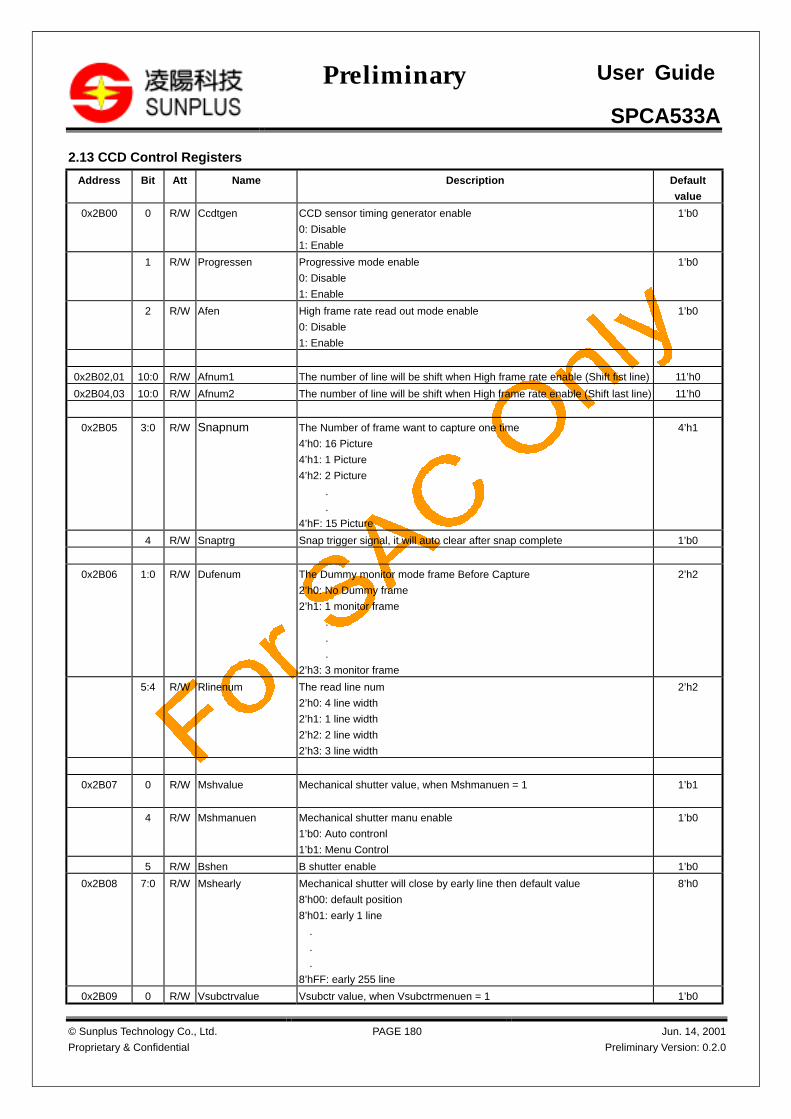
SPCA533A
© Sunplus Technology Co., Ltd.
Proprietary & Confidential
PAGE 180 Jun. 14, 2001
Preliminary Version: 0.2.0
Preliminary User Guide
2.13 CCD Control Registers
Address Bit Att Name Description Default
value
0x2B00 0 R/W Ccdtgen CCD sensor timing generator enable
0: Disable
1: Enable
1’b0
1 R/W Progressen Progressive mode enable
0: Disable
1: Enable
1’b0
2 R/W Afen High frame rate read out mode enable
0: Disable
1: Enable
1’b0
0x2B02,01 10:0 R/W Afnum1 The number of line will be shift when High frame rate enable (Shift fist line) 11’h0
0x2B04,03 10:0 R/W Afnum2 The number of line will be shift when High frame rate enable (Shift last line) 11’h0
0x2B05 3:0 R/W Snapnum The Number of frame want to capture one time
4’h0: 16 Picture
4’h1: 1 Picture
4’h2: 2 Picture
.
.
4’hF: 15 Picture
4’h1
4 R/W Snaptrg Snap trigger signal, it will auto clear after snap complete 1’b0
0x2B06 1:0 R/W Dufenum The Dummy monitor mode frame Before Capture
2’h0: No Dummy frame
2’h1: 1 monitor frame
.
.
.
2’h3: 3 monitor frame
2’h2
5:4 R/W Rlinenum The read line num
2’h0: 4 line width
2’h1: 1 line width
2’h2: 2 line width
2’h3: 3 line width
2’h2
0x2B07 0 R/W Mshvalue Mechanical shutter value, when Mshmanuen = 1 1’b1
4 R/W Mshmanuen Mechanical shutter manu enable
1’b0: Auto contronl
1’b1: Menu Control
1’b0
5 R/W Bshen B shutter enable 1’b0
0x2B08 7:0 R/W Mshearly Mechanical shutter will close by early line then default value
8’h00: default position
8’h01: early 1 line
.
.
.
8’hFF: early 255 line
8’h0
0x2B09 0 R/W Vsubctrvalue Vsubctr value, when Vsubctrmenuen = 1 1’b0

SPCA533A
© Sunplus Technology Co., Ltd.
Proprietary & Confidential
PAGE 181 Jun. 14, 2001
Preliminary Version: 0.2.0
Preliminary User Guide
4 R/W Vsubctrmenuen Vsubctr menu enable
1’b0: Auto contronl
1’b1: Menu Control
1’b0
0x2B0B,0A 11:0 R/W Esptime Exposure time (The unit is line) 12’h64
0x2B10 0 R/W Fh1pol The Fh1 polarity will be inverted when this bit set 1’b0
1 R/W Fh2pol The Fh2 polarity will be inverted when this bit set 1’b0
2 R/W Subpol The Sub polarity will be inverted when this bit set 1’b0
3 R/W Clpobpol The Clpob polarity will be inverted when this bit set 1’b0
4 R/W Clpdmpol The Clpdm polarity will be inverted when this bit set 1’b0
5 R/W Pblkpol The pblk polarity will be inverted when this bit set 1’b0
6 R/W CCDfldpol The CCD field pol 1’b0
0x2B11 0 R/W Xv1pol The Xv1 polarity will be inverted when this bit set 1’b0
1 R/W Xv2pol The Xv2 polarity will be inverted when this bit set 1’b0
2 R/W Xv3pol The Xv3 polarity will be inverted when this bit set 1’b0
3 R/W Xv4pol The Xv4 polarity will be inverted when this bit set 1’b0
4 R/W Xsg1apol The Xsg1a polarity will be inverted when this bit set 1’b0
5 R/W Xsg1bpol The Xsg1b polarity will be inverted when this bit set 1’b0
6 R/W Xsg3apol The Xsg3a polarity will be inverted when this bit set 1’b0
7 R/W Xsg3bpol The Xsg3b polarity will be inverted when this bit set 1’b0
0x2B12 0 R/W Rgpol The Rg polarity will be inverted when this bit set 1’b0
1 R/W Xshppol The Xshp polarity will be inverted when this bit set 1’b0
2 R/W Xshdpol The Xshd polarity will be inverted when this bit set 1’b0
3 R/W Mshutterpol The mechanical shutter control signal polarity will be inverted when this bit
set
1’b0
4 R/W Vsubctrpol The Vsubctr control signal polarity will be inverted when this bit set 1’b0
0x2B13 4:0 R/W RgDelay The Rg signal delay parameter:
5’h00: No delay
5’h01: Delay 1ns
.
.
5’h0F: Delay 31ns
5’h0
0x2B14 1:0 R/W Rgpos The Rg signal Low Position between clk 2’h3
0x2B15 4:0 R/W Xshpdelay The Xshp signal delay parameter:
5’h00: No delay
5’h01: Delay 1ns
.
.
5’h1F: Delay 31s
5’h0
0x2B16 1:0 R/W Xshppos The Xshp signal Low Position between clk 2’h0
0x2B17 4:0 R/W Xshddelay The Xshd signal delay parameter:
5’h00: No delay
5’h01: Delay 1s
.
5’h1F: Delay 31ns
5’h0
0x2B18 1:0 R/W Xshdpos The Xshd signal Low Position between clk 2’h2
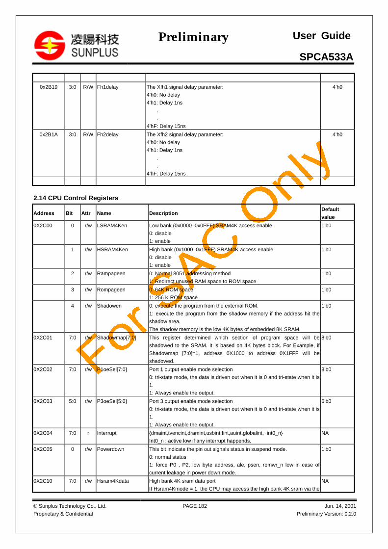
SPCA533A
© Sunplus Technology Co., Ltd.
Proprietary & Confidential
PAGE 182 Jun. 14, 2001
Preliminary Version: 0.2.0
Preliminary User Guide
0x2B19 3:0 R/W Fh1delay The Xfh1 signal delay parameter:
4’h0: No delay
4’h1: Delay 1ns
.
.
4’hF: Delay 15ns
4’h0
0x2B1A 3:0 R/W Fh2delay The Xfh2 signal delay parameter:
4’h0: No delay
4’h1: Delay 1ns
.
.
4’hF: Delay 15ns
4’h0
2.14 CPU Control Registers
Address Bit Attr Name DescriptionDefault
value
0X2C00 0 r/w LSRAM4Ken Low bank (0x0000–0x0FFF) SRAM4K access enable
0: disable
1: enable
1’b0
1 r/w HSRAM4Ken High bank (0x1000–0x1FFF) SRAM4K access enable
0: disable
1: enable
1’b0
2 r/w Rampageen 0: Normal 8051 addressing method
1: Redirect unused RAM space to ROM space
1’b0
3 r/w Rompageen 0: 64K ROM space
1: 256 K ROM space
1’b0
4 r/w Shadowen 0: execute the program from the external ROM.
1: execute the program from the shadow memory if the address hit the
shadow area.
The shadow memory is the low 4K bytes of embedded 8K SRAM.
1’b0
0X2C01 7:0 r/w Shadowmap[7:0] This register determined which section of program space will be
shadowed to the SRAM. It is based on 4K bytes block. For Example, if
Shadowmap [7:0]=1, address 0X1000 to address 0X1FFF will be
shadowed.
8’b0
0X2C02 7:0 r/w P1oeSel[7:0] Port 1 output enable mode selection
0: tri-state mode, the data is driven out when it is 0 and tri-state when it is
1.
1: Always enable the output.
8’b0
0X2C03 5:0 r/w P3oeSel[5:0] Port 3 output enable mode selection
0: tri-state mode, the data is driven out when it is 0 and tri-state when it is
1.
1: Always enable the output.
6’b0
0X2C04 7:0 r Interrupt {dmaint,tvencint,dramint,usbint,fint,auint,globalint,~int0_n}
Int0_n : active low if any interrupt happends.
NA
0X2C05 0 r/w Powerdown This bit indicate the pin out signals status in suspend mode.
0: normal status
1: force P0 , P2, low byte address, ale, psen, romwr_n low in case of
current leakage in power down mode.
1’b0
0X2C10 7:0 r/w Hsram4Kdata High bank 4K sram data port
If Hsram4Kmode = 1, the CPU may access the high bank 4K sram via the
NA
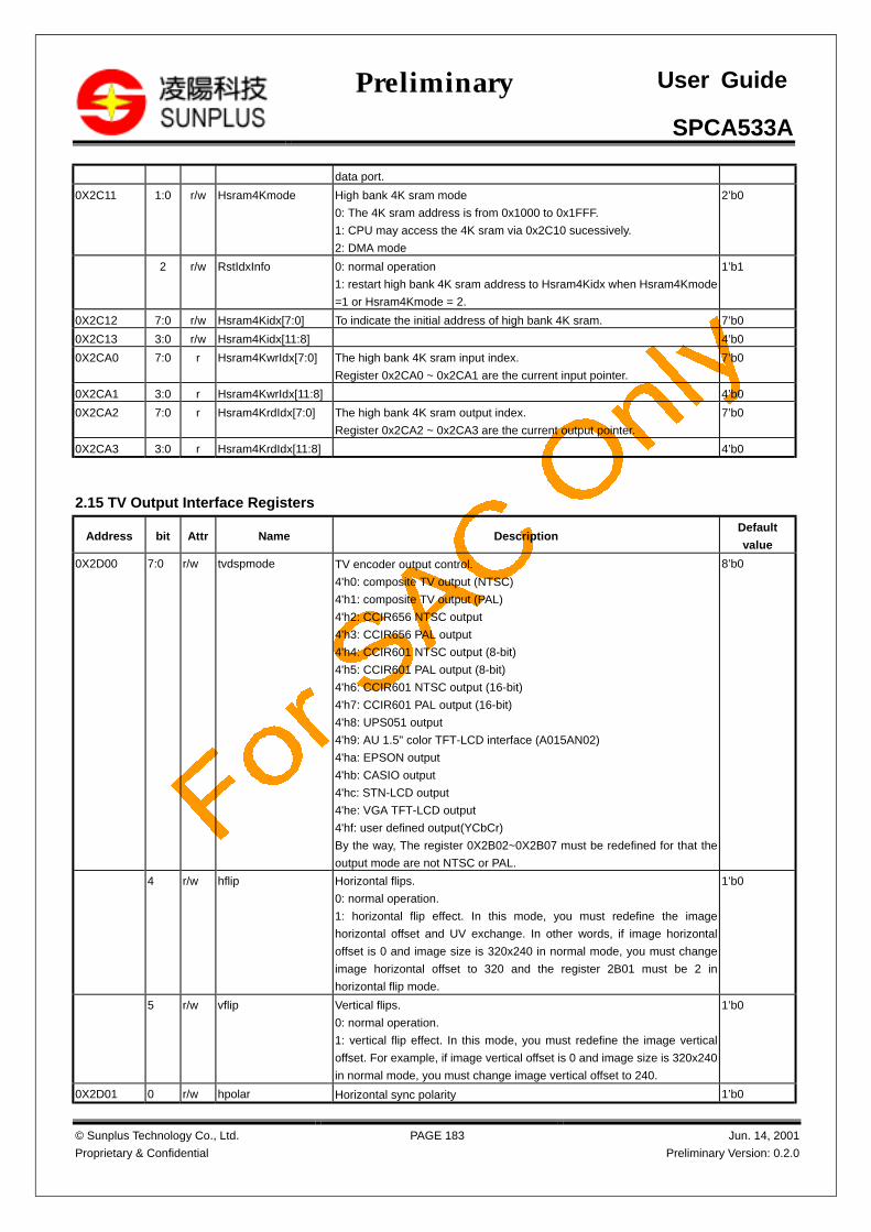
SPCA533A
© Sunplus Technology Co., Ltd.
Proprietary & Confidential
PAGE 183 Jun. 14, 2001
Preliminary Version: 0.2.0
Preliminary User Guide
data port.
0X2C11 1:0 r/w Hsram4Kmode High bank 4K sram mode
0: The 4K sram address is from 0x1000 to 0x1FFF.
1: CPU may access the 4K sram via 0x2C10 sucessively.
2: DMA mode
2’b0
2 r/w RstIdxInfo 0: normal operation
1: restart high bank 4K sram address to Hsram4Kidx when Hsram4Kmode
=1 or Hsram4Kmode = 2.
1’b1
0X2C12 7:0 r/w Hsram4Kidx[7:0] To indicate the initial address of high bank 4K sram. 7’b0
0X2C13 3:0 r/w Hsram4Kidx[11:8] 4’b0
0X2CA0 7:0 r Hsram4KwrIdx[7:0] The high bank 4K sram input index.
Register 0x2CA0 ~ 0x2CA1 are the current input pointer.
7’b0
0X2CA1 3:0 r Hsram4KwrIdx[11:8] 4’b0
0X2CA2 7:0 r Hsram4KrdIdx[7:0] The high bank 4K sram output index.
Register 0x2CA2 ~ 0x2CA3 are the current output pointer.
7’b0
0X2CA3 3:0 r Hsram4KrdIdx[11:8] 4’b0
2.15 TV Output Interface Registers
Address bit Attr Name DescriptionDefault
value
0X2D00 7:0 r/w tvdspmode TV encoder output control.
4'h0: composite TV output (NTSC)
4'h1: composite TV output (PAL)
4'h2: CCIR656 NTSC output
4'h3: CCIR656 PAL output
4'h4: CCIR601 NTSC output (8-bit)
4'h5: CCIR601 PAL output (8-bit)
4'h6: CCIR601 NTSC output (16-bit)
4'h7: CCIR601 PAL output (16-bit)
4'h8: UPS051 output
4'h9: AU 1.5" color TFT-LCD interface (A015AN02)
4'ha: EPSON output
4'hb: CASIO output
4'hc: STN-LCD output
4'he: VGA TFT-LCD output
4'hf: user defined output(YCbCr)
By the way, The register 0X2B02~0X2B07 must be redefined for that the
output mode are not NTSC or PAL.
8’b0
4 r/w hflip Horizontal flips.
0: normal operation.
1: horizontal flip effect. In this mode, you must redefine the image
horizontal offset and UV exchange. In other words, if image horizontal
offset is 0 and image size is 320x240 in normal mode, you must change
image horizontal offset to 320 and the register 2B01 must be 2 in
horizontal flip mode.
1’b0
5 r/w vflip Vertical flips.
0: normal operation.
1: vertical flip effect. In this mode, you must redefine the image vertical
offset. For example, if image vertical offset is 0 and image size is 320x240
in normal mode, you must change image vertical offset to 240.
1’b0
0X2D01 0 r/w hpolar Horizontal sync polarity 1’b0
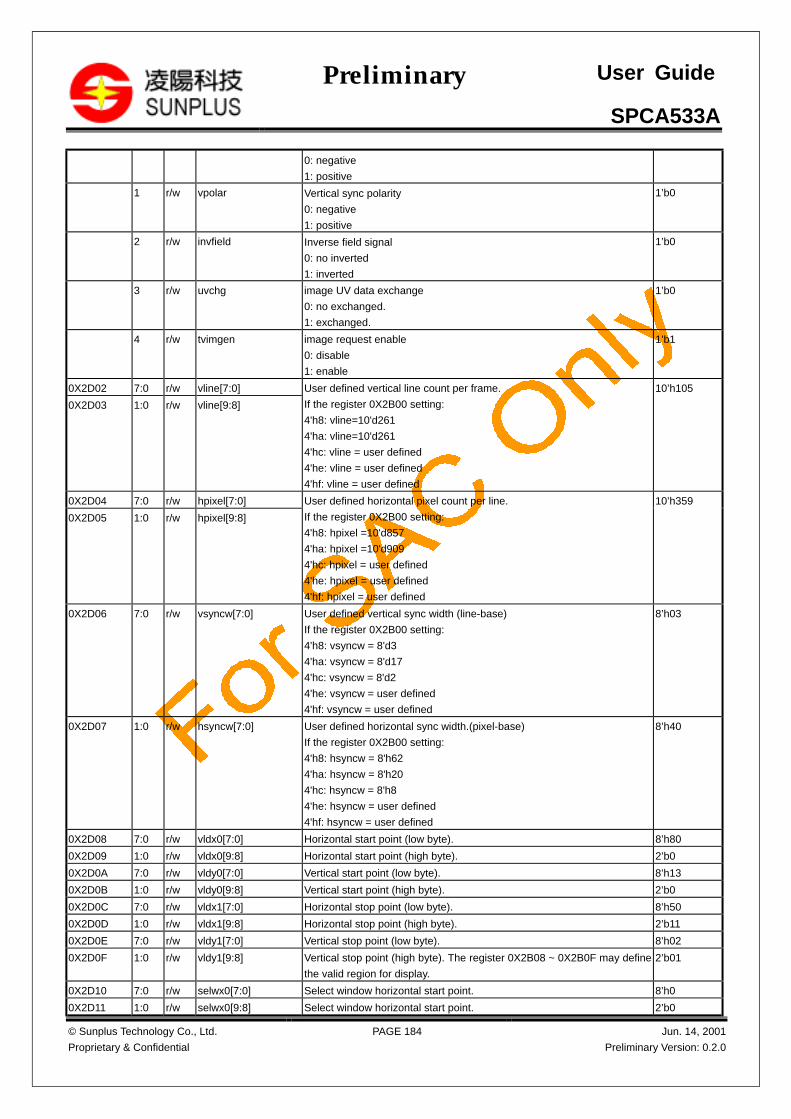
SPCA533A
© Sunplus Technology Co., Ltd.
Proprietary & Confidential
PAGE 184 Jun. 14, 2001
Preliminary Version: 0.2.0
Preliminary User Guide
0: negative
1: positive
1 r/w vpolar Vertical sync polarity
0: negative
1: positive
1’b0
2 r/w invfield Inverse field signal
0: no inverted
1: inverted
1’b0
3 r/w uvchg image UV data exchange
0: no exchanged.
1: exchanged.
1’b0
4 r/w tvimgen image request enable
0: disable
1: enable
1’b1
0X2D02 7:0 r/w vline[7:0]
0X2D03 1:0 r/w vline[9:8]
User defined vertical line count per frame.
If the register 0X2B00 setting:
4'h8: vline=10'd261
4'ha: vline=10'd261
4'hc: vline = user defined
4'he: vline = user defined
4'hf: vline = user defined
10’h105
0X2D04 7:0 r/w hpixel[7:0]
0X2D05 1:0 r/w hpixel[9:8]
User defined horizontal pixel count per line.
If the register 0X2B00 setting:
4'h8: hpixel =10'd857
4'ha: hpixel =10'd909
4'hc: hpixel = user defined
4'he: hpixel = user defined
4'hf: hpixel = user defined
10’h359
0X2D06 7:0 r/w vsyncw[7:0] User defined vertical sync width (line-base)
If the register 0X2B00 setting:
4'h8: vsyncw = 8'd3
4'ha: vsyncw = 8'd17
4'hc: vsyncw = 8'd2
4'he: vsyncw = user defined
4'hf: vsyncw = user defined
8’h03
0X2D07 1:0 r/w hsyncw[7:0] User defined horizontal sync width.(pixel-base)
If the register 0X2B00 setting:
4'h8: hsyncw = 8'h62
4'ha: hsyncw = 8'h20
4'hc: hsyncw = 8'h8
4'he: hsyncw = user defined
4'hf: hsyncw = user defined
8’h40
0X2D08 7:0 r/w vldx0[7:0] Horizontal start point (low byte). 8’h80
0X2D09 1:0 r/w vldx0[9:8] Horizontal start point (high byte). 2’b0
0X2D0A 7:0 r/w vldy0[7:0] Vertical start point (low byte). 8’h13
0X2D0B 1:0 r/w vldy0[9:8] Vertical start point (high byte). 2’b0
0X2D0C 7:0 r/w vldx1[7:0] Horizontal stop point (low byte). 8’h50
0X2D0D 1:0 r/w vldx1[9:8] Horizontal stop point (high byte). 2’b11
0X2D0E 7:0 r/w vldy1[7:0] Vertical stop point (low byte). 8’h02
0X2D0F 1:0 r/w vldy1[9:8] Vertical stop point (high byte). The register 0X2B08 ~ 0X2B0F may define
the valid region for display.
2’b01
0X2D10 7:0 r/w selwx0[7:0] Select window horizontal start point. 8’h0
0X2D11 1:0 r/w selwx0[9:8] Select window horizontal start point. 2’b0

SPCA533A
© Sunplus Technology Co., Ltd.
Proprietary & Confidential
PAGE 185 Jun. 14, 2001
Preliminary Version: 0.2.0
Preliminary User Guide
0X2D12 7:0 r/w selwy0[7:0] Select window vertical start point. 8’h0
0X2D13 1:0 r/w selwy0[9:8] Select window vertical start point. 2’b0
0X2D14 7:0 r/w selwx1[7:0] Select window horizontal stop point. 8’h0
0X2D15 1:0 r/w selwx1[9:8] Select window horizontal stop point. 2’b0
0X2D16 7:0 r/w selwy1[7:0] Select window vertical stop point. 8’h0
0X2D17 1:0 r/w selwy1[9:8] Select window vertical stop point. 2’b0
0X2D18 3:0 r/w selwsiz[3:0] Select window width. If selwsiz=4'hf, the selected region will perform in
OSD special function effect.
4’b0
6:4 r/w selwclr[2:0] Select window color.
0:R=color0r; G=color0g; B=color0b
1:R=color1r; G=color1g; B=color1b
2:R=color2r; G=color2g; B=color2b
3:R=color3r; G=color3g; B=color3b
4:R=color4r; G=color4g; B=color4b
5:R=color5r; G=color5g; B=color5b
6:R=color6r; G=color6g; B=color6b
7:R=color7r; G=color7g; B=color7b
3’b0
7 r/w selwen Select window enable.
0: disable
1: enable
2’b0
0X2D19 7:0 r/w imgvzfac[7:0] Image vertical zoom factor.
imgvzfac = (image lines)/(display lines)*32. For example, image size is
320x240 and display size is 280x220, the imgvzfac is (240/220)*32 = 34
8’h40
0X2D1A 7:0 r/w imghzfac[7:0] Image horizontal zoom factor.
imghzfac = (image pixels)/(display dots)*128. For example, image size is
320x240 and display size is 280x220, the imghzfac is (320/280)*128 =
146.
8’h80
0X2D1B 7:0 r/w imgvofst[7:0] Image vertical offset. 8’h0
0X2D1C 3:0 r/w imgvofst[11:8] Image vertical offset. 4’h0
0X2D1D 7:0 r/w imghofst[7:0] Image horizontal offset. 8’h0
0X2D1E 3:0 r/w imghofst[11:8] Image horizontal offset. 4’h0
0X2D1F 5:0 r/w imghpix[5:0] Image horizontal pixel counts.
imghpix = (image pixels/16). For example, image size is 320x240, imghpix
= (320/16) = 20
6’h0
0X2D20 6:0 r/w imgsubsamp[6:0] Image sub-sample factor. (for future use) 7’h40
0X2D21 6:0 r/w osdsubsamp[6:0] OSD sub-sample factor. osdsubsamp = 7'h20 for TV and osdsubsamp =
7'h40 for LCD.
7’h40
0X2D22 7:0 r/w saturate Saturation adjustment (only for analog TV) 8’h1c
0X2D23 7:0 r/w hueadjust Hue adjustment (only for analog TV) 8’h0
0X2D25 2:0 r/w xsclstate EPSON XSCL state defines. 3’h0
3 r/w em1812en EPSON LCD controller em1812b function enable. 1’h0
4 r/w wscrnen CASIO white screen enable.
0: disable
1:enable
1’h0
5 r/w gresctrl CASIO GRES signal controller.
0: output low.
1:normal operation
1’h0
6 r/w stbybctrl CASIO stand-by controller.
0:normal operation
1: stand-by mode.
1’h0
7 r/w ritctrl CASIO RIT signal controller.
0: Normal display mode.
1’h0

SPCA533A
© Sunplus Technology Co., Ltd.
Proprietary & Confidential
PAGE 186 Jun. 14, 2001
Preliminary Version: 0.2.0
Preliminary User Guide
1:Horizontally flipped display mode.
0X2D26 1:0 r/w oddrgb TFT-LCD odd lines RGB cycle define.
0: RGB
1: RGB
2: GBR
3: BRG
2’h0
3:2 r/w evenrgb TFT-LCD even lines RGB cycle define.
0: GBR
1: GBR
2: BRG
3: RGB
2’h0
0X2D27 3:0 r/w lp_position STN-LCD LP signal position defines. 8’h0
7:4 r/w eio1_position STN-LCD EIO1 signal position defines. 8’h0
0X2D28 7:0 r/w fr_ctrl STN-LCD FR control signal. 8’h0
0X2D29 1:0 r/w xck_sel STN-LCD XCK select signal. 2’h0
3:2 r/w filter_type STN-LCD filter type select signal
0: RGBRGB
BRGBRG
1: RGRGRG
GBGBGB
BRBRBR
2: RGBRGB
RGBRGB
3: RBRBRB
GRGRGR
BGBGBG
2’h0
0X2D2A 1:0 r/w ccirtype define CCIR output sequence
0: YCrYCb
1: CrYCbY
2: YCbYCr
3: CbYCrY
2’h0
0X2D2B 0 r/w gammaen Gamma enable.
0: disable.
1: enable.
1’h0
1 r/w dien Dither enable.
0: disable
1:enable
1’h0
2 r/w osdlpfen OSD low-pass filter enable
0: disable
1: enable
1’h0
0X2D2C 0 r/w sramhbyte SRAM high byte value (only for SRAM256x9). 1’h0
1 r/w sram256x9en SRAM256x9 access enable. 1’h0
2 r/w sram256x6en SRAM256x6 access enable. 1’h0
0X2D2D 7:0 r/w sramaddr SRAM address 8’h0
0X2D2E 7:0 r/w sramdata SRAM data. For example, write 9'h120 to SRAM256x9, the register
2B62=3 first and then write the register 2B64=20.
8’h0
0X2D2F 6:0 r/w colorkey Color key defines.
If image's luminance smaller than color key defined value, encoder will
show the OSD color.
8’h0
7 r/w colorkeyen Color key enable.
0: disable
1: enable
8’h0
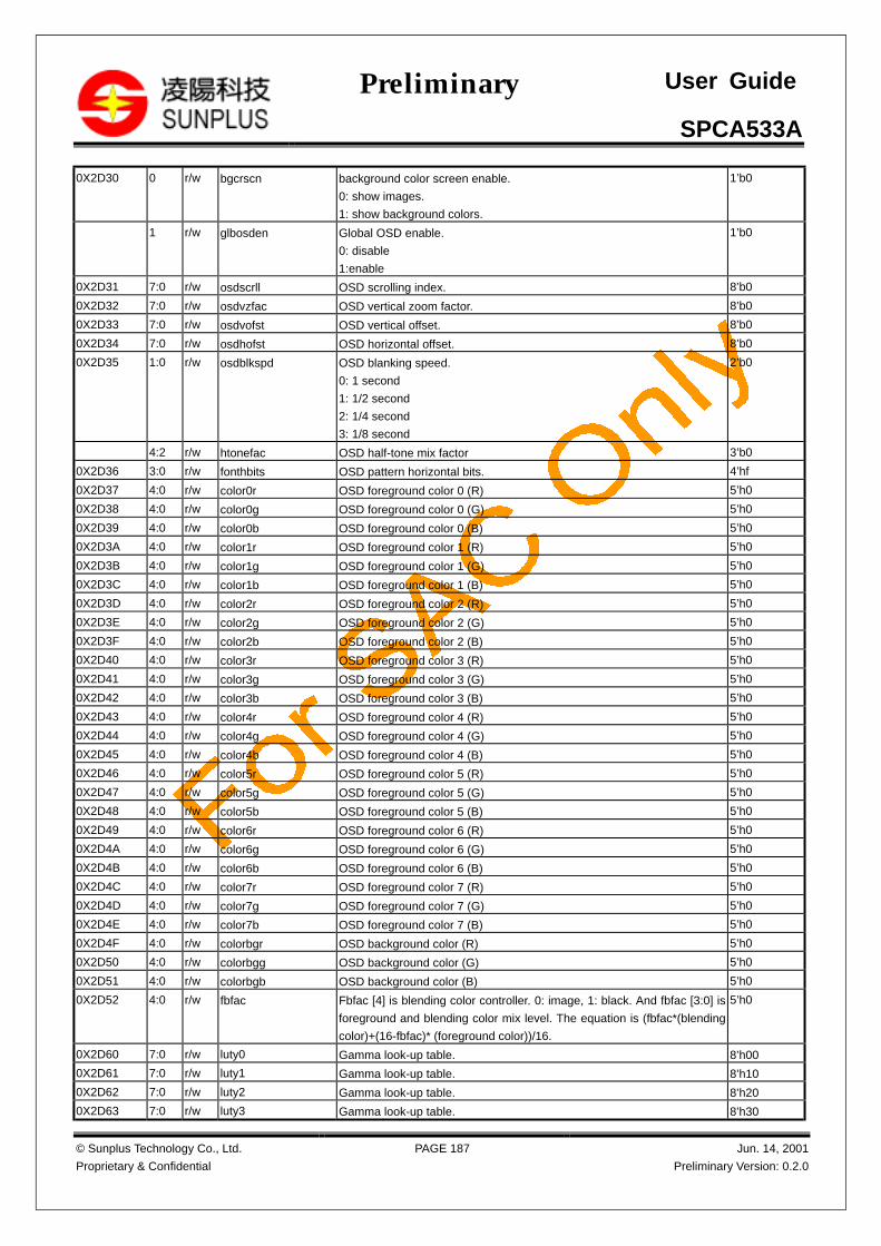
SPCA533A
© Sunplus Technology Co., Ltd.
Proprietary & Confidential
PAGE 187 Jun. 14, 2001
Preliminary Version: 0.2.0
Preliminary User Guide
0X2D30 0 r/w bgcrscn background color screen enable.
0: show images.
1: show background colors.
1’b0
1 r/w glbosden Global OSD enable.
0: disable
1:enable
1’b0
0X2D31 7:0 r/w osdscrll OSD scrolling index. 8’b0
0X2D32 7:0 r/w osdvzfac OSD vertical zoom factor. 8’b0
0X2D33 7:0 r/w osdvofst OSD vertical offset. 8’b0
0X2D34 7:0 r/w osdhofst OSD horizontal offset. 8’b0
0X2D35 1:0 r/w osdblkspd OSD blanking speed.
0: 1 second
1: 1/2 second
2: 1/4 second
3: 1/8 second
2’b0
4:2 r/w htonefac OSD half-tone mix factor 3’b0
0X2D36 3:0 r/w fonthbits OSD pattern horizontal bits. 4’hf
0X2D37 4:0 r/w color0r OSD foreground color 0 (R) 5’h0
0X2D38 4:0 r/w color0g OSD foreground color 0 (G) 5’h0
0X2D39 4:0 r/w color0b OSD foreground color 0 (B) 5’h0
0X2D3A 4:0 r/w color1r OSD foreground color 1 (R) 5’h0
0X2D3B 4:0 r/w color1g OSD foreground color 1 (G) 5’h0
0X2D3C 4:0 r/w color1b OSD foreground color 1 (B) 5’h0
0X2D3D 4:0 r/w color2r OSD foreground color 2 (R) 5’h0
0X2D3E 4:0 r/w color2g OSD foreground color 2 (G) 5’h0
0X2D3F 4:0 r/w color2b OSD foreground color 2 (B) 5’h0
0X2D40 4:0 r/w color3r OSD foreground color 3 (R) 5’h0
0X2D41 4:0 r/w color3g OSD foreground color 3 (G) 5’h0
0X2D42 4:0 r/w color3b OSD foreground color 3 (B) 5’h0
0X2D43 4:0 r/w color4r OSD foreground color 4 (R) 5’h0
0X2D44 4:0 r/w color4g OSD foreground color 4 (G) 5’h0
0X2D45 4:0 r/w color4b OSD foreground color 4 (B) 5’h0
0X2D46 4:0 r/w color5r OSD foreground color 5 (R) 5’h0
0X2D47 4:0 r/w color5g OSD foreground color 5 (G) 5’h0
0X2D48 4:0 r/w color5b OSD foreground color 5 (B) 5’h0
0X2D49 4:0 r/w color6r OSD foreground color 6 (R) 5’h0
0X2D4A 4:0 r/w color6g OSD foreground color 6 (G) 5’h0
0X2D4B 4:0 r/w color6b OSD foreground color 6 (B) 5’h0
0X2D4C 4:0 r/w color7r OSD foreground color 7 (R) 5’h0
0X2D4D 4:0 r/w color7g OSD foreground color 7 (G) 5’h0
0X2D4E 4:0 r/w color7b OSD foreground color 7 (B) 5’h0
0X2D4F 4:0 r/w colorbgr OSD background color (R) 5’h0
0X2D50 4:0 r/w colorbgg OSD background color (G) 5’h0
0X2D51 4:0 r/w colorbgb OSD background color (B) 5’h0
0X2D52 4:0 r/w fbfac Fbfac [4] is blending color controller. 0: image, 1: black. And fbfac [3:0] is
foreground and blending color mix level. The equation is (fbfac*(blending
color)+(16-fbfac)* (foreground color))/16.
5’h0
0X2D60 7:0 r/w luty0 Gamma look-up table. 8’h00
0X2D61 7:0 r/w luty1 Gamma look-up table. 8’h10
0X2D62 7:0 r/w luty2 Gamma look-up table. 8’h20
0X2D63 7:0 r/w luty3 Gamma look-up table. 8’h30

SPCA533A
© Sunplus Technology Co., Ltd.
Proprietary & Confidential
PAGE 188 Jun. 14, 2001
Preliminary Version: 0.2.0
Preliminary User Guide
0X2D64 7:0 r/w luty4 Gamma look-up table. 8’h40
0X2D65 7:0 r/w luty5 Gamma look-up table. 8’h50
0X2D66 7:0 r/w luty6 Gamma look-up table. 8’h60
0X2D67 7:0 r/w luty7 Gamma look-up table. 8’h70
0X2D68 7:0 r/w luty8 Gamma look-up table. 8’h80
0X2D69 7:0 r/w luty9 Gamma look-up table. 8’h90
0X2D6A 7:0 r/w lutya Gamma look-up table. 8’ha0
0X2D6B 7:0 r/w lutyb Gamma look-up table. 8’hb0
0X2D6C 7:0 r/w lutyc Gamma look-up table. 8’hc0
0X2D6D 7:0 r/w lutyd Gamma look-up table. 8’hd0
0X2D6E 7:0 r/w lutye Gamma look-up table. 8’he0
0X2D6F 7:0 r/w lutyf Gamma look-up table. 8’hf0
0X2D70 7:0 r/w luty10 Gamma look-up table. 8’hff
0X2D71 7:0 r/w tvegpioo[7:0] TV encoder GPIO output data. 8’h0
0X2D72 7:0 r/w tvegpioo[15:8] TV encoder GPIO output data. 8’h0
0X2D73 5:0 r/w tvegpioo[21:16] TV encoder GPIO output data. 6’h0
0X2D74 7:0 r/w tvegpiooe[7:0] TV encoder GPIO output enable. 8’h0
0X2D75 7:0 r/w tvegpiooe[15:8] TV encoder GPIO output enable. 8’h0
0X2D76 5:0 r/w tvegpiooe[21:16] TV encoder GPIO output enable. 6’h0
0X2DA0 0 r hvalid TV encoder horizontal valid signal.
1 r hsync TV encoder horizontal sync signal.
2 r vvalid TV encoder vertical valid signal.
3 r vsync TV encoder vertical sync signal.
4 r tvencframe TV encoder frame signal.
0X2DC0 0 w vdrevt TV encoder vsync interrupt signal.
The interrupt is generated when the corresponding vsync goes from low to
high. Write 0 to the register will clear the interrupt. Write 1 to the register
has no impact on the interrupt values.
1 w vdfevt TV encoder vsync interrupt signal.
The interrupt is generated when the corresponding vsync goes from high
to low. Write 0 to the register will clear the interrupt. Write 1 to the register
has no impact on the interrupt values.
0X2DC1 7:0 r/w digrevt[7:0] TV encoder digtvi[7:0] interrupt signal.
The interrupt is generated when the corresponding digtvi ports goes from
low to high. Write 0 to the register will clear the interrupt. Write 1 to the
register has no impact on the interrupt values.
0X2DC2 7:0 r/w digrevt [15:8] TV encoder digtvi[15:8] interrupt signal.
0X2DC3 5:0 r/w digrevt [21:16] TV encoder digtvi[21:16] interrupt signal.
0X2DC4 7:0 r/w digfevt[7:0] TV encoder digtvi[7:0] interrupt signal.
The interrupt is generated when the corresponding digtvi ports goes from
high to low. Write 0 to the register will clear the interrupt. Write 1 to the
register has no impact on the interrupt values.
0X2DC5 7:0 r/w digfevt [15:8] TV encoder digtvi[15:8] interrupt signal.
0X2DC6 5:0 r/w digfevt [21:16] TV encoder digtvi[21:16] interrupt signal.
0X2DC7 7:0 r/w digtvi[7:0] TV encoder digtvi[7:0] input values.
0X2DC8 7:0 r/w digtvi[15:8] TV encoder digtvi[15:8] input values.
0X2DC9 5:0 r/w digtvi[21:16] TV encoder digtvi[21:16] input values.
0X2DD0 0 r/w vdfinten TV encoder vertical sync falling edge interrupt enable. 1’h0
1 r/w vdrinten TV encoder vertical sync rising edge interrupt enable. 1’h0
0X2DD1 7:0 r/w rinten[7:0] TV encoder digtvi[7:0] rising edge interrupt enable. 8'h0
0X2DD2 7:0 r/w rinten[15:8] TV encoder digtvi[15:8] rising edge interrupt enable. 8'h0

SPCA533A
© Sunplus Technology Co., Ltd.
Proprietary & Confidential
PAGE 189 Jun. 14, 2001
Preliminary Version: 0.2.0
Preliminary User Guide
0X2DD3 5:0 r/w rinten[21:16] TV encoder digtvi[21:16] rising edge interrupt enable. 6'h0
0X2DD4 7:0 r/w finten[7:0] TV encoder digtvi[7:0] falling edge interrupt enable. 8'h0
0X2DD5 7:0 r/w finten[15:8] TV encoder digtvi[15:8] falling edge interrupt enable. 8'h0
0X2DD6 5:0 r/w finten[21:16] TV encoder digtvi[21:16] falling edge interrupt enable. 6'h0
0X2DE2 7:0 r/w tverctrl[7:0] Bit[0]: frame rate conversion control. 0: field mode, 1: frame mode.
Bit[1]: luminance filter controller. 0: enable. 1: disable
Bit[2]: CASIO interface option.
8’h0
3. Application/Usage Descriptions (by FAE)
SPCA533A
© Sunplus Technology Co., Ltd.
Proprietary & Confidential
PAGE 190 Jun. 14, 2001
Preliminary Version: 0.2.0
Preliminary User Guide
REVISION HISTORY
Date Revision # Description Page
Nov. 01, 2001 0.1.0 First draft
Jan. 02, 2002 0.1.2 Editorial Modification
Mar. 11, 2002 0.1.3 The onextal pin number shall be B13(280) instead of V11(280) in the clock setting table p. 7
Jun. 14, 2002 0.2.0 Add 3-field CCD control registers (0x2924 and 0x2926)
Add video control register 0x2DE2
Add volume control register 0x2676
Add USB power configuration register 0x20E8
Add Q-Table access register 0x2882
p. 176
p. 189
p.165
p.141
p.173