superconductivity in thebi/nibilayer - arxiv
TRANSCRIPT

arX
iv:1
808.
0533
3v2
[co
nd-m
at.s
tr-e
l] 2
7 M
ar 2
019
Superconductivity in the Bi/Ni bilayer
Sung-Po ChaoDepartment of Physics, National Kaohsiung Normal University, Kaohsiung 82444, Taiwan, R.O.C.
(Dated: March 28, 2019)
Motivated by the recent observations of possible p-wave superconductivity in the bismuth-nickel(Bi/Ni) bilayer, we explore theoretically the possibilities of realizing p-wave superconductivity inthis bilayer. We begin with a literature survey on this system and related materials which havesimilar superconducting transition temperature. From the survey the superconducting mechanismin this bilayer system is suggested to be phonon mediated type II superconductivity. A simplemodel is proposed to explain why the p-wave like Andreev reflection signals are likely to be observedin the surface probe, assuming the strong spin-orbit coupled surface state of Bi thin film is notcompletely destroyed by the formation of alloys.
PACS numbers: 74.78.Fk
I. INTRODUCTION
The search for the possibility of realizing the simplestNon Abelian anyon, the Majorana zero modes1,2 in thevortex state of topological superconductors, has beenone of the hottest topics in the field of condensed matter.One way to achieve this topological superconductor isto search for superconductors with broken time reversalsymmetry (TRS), implying the possible coexistence offerromagnetism and superconductivity. Such coexistencehas been reported in some heavy fermion materials,including UGe2
3, URhGe4, UCoGe5, Sr2RuO4, etc.Among them Sr2RuO4 is perhaps the most extensivelystudied candidate of chiral p-wave superconductor, inwhich anomalous responses to external magnetic fieldand the appearance of half flux quantum has beenreported. However, the lack of clear evidences for chiraledge current, a key signature for chiral superconduc-tivity, has made the claim of Sr2RuO4 being a p-wavesuperconductor less conclusive.
An alternative approach is to make artificial struc-tures to realize such TRS broken superconductivity.Early proposals focus on the proximity effect betweens-wave superconductor and ferromagnetic metal6,7 byartificially fabricating superconductor/ferromagnet(S/F)heterostructures. Numerous peculiar behaviors havebeen found in such systems such as spatial oscillation ofelectronic density of states, oscillatory superconductingtransition temperature, and π phase in Josephsonjunction to name a few. Recently with the emergenceof topological insulators, it is proposed to use spin orbitcoupled surface state of magnetic impurities doped topo-logical insulators, or some semiconductors with strongspin orbit interactions placing in close proximity to aconventional superconductor combined with externalmagnetic field to achieve topological superconductivity.Zero bias anomaly8 in the tunneling differential conduc-tance from the transport measurement is viewed as oneof the important indications of obtaining Majorana zeromodes. This zero bias anomaly has been experimentally
observed in several candidate systems, including thepoint contact Andreev reflection spectra on the Bismuthsurface of epitaxially grown Bismuth/Nickel (Bi/Ni)bilayer thin film observed by X. X. Gong et al.9 in 2015.
Bismuth/Nickel (Bi/Ni) bilayer film is viewed asone of the S/F heterostructures10,11, but it is not aconventional S/F heterostructure as neither crystallineBi nor Ni becomes superconducting above 1K at ambi-ent pressure. Bulk crystalline Bi at ambient pressureenters into superconducting phase12 at temperaturebelow 0.53mK due to its low carrier density. Makingamorphous or polycrystalline Bi enhances the carrierdensity of state and the electron phonon interactions,brining up the superconducting transition temperatureTc to 5 ∼ 6 K at ambient pressure. Similar enhancementis also achieved through placing single crystal under highpressure. Ni is a weak ferromagnetic metal, which showsno traces of superconductivity down to any measurabletemperature. In 1990, it is found by J. S. Moodera andR. Meservey10 that growing thin film of Bi on top ofNi thin film makes Bi side superconduct with optimalTc ≃ 4K. In 2015, X. X. Gong et al.9 find zero biasanomaly which sustains even under high magnetic fieldin their transport measurement on the Bi/Ni thin film.
In our model, we assume that the observed supercon-ductivity in Bi/Ni is of conventional phonon mediatedtype and existing in the bulk of Bi thin film. This issupported by previous experimental reports13–15 showingtraces of alloyic Bi3Ni formed throughout the Bi, eventhough this randomly distributed amount of alloys maynot be significant enough to distort the X-ray diffractionimages. That is, those diffusively formed randomimpurities do not significantly blur the rhombohedralstructure in the Bi layer observed using transmissionelectron microscopy or X-ray diffraction. This alloyicBi3Ni has superconducting transition temperaturearound 4K and is a type II superconductor16. Thoseproperties explain why this Bi/Ni superconductivitycould sustain with Ni thickness increasing up to around

2
1/5 of the Bi thickness, and the reason for the maximaltransition temperature in this bilayer is around 4K.The remaining puzzle is then the zero bias anomalyseen in the Andreev reflection signals9 observed on theBi surface away from the Bi/Ni interface. We proposea simple theoretical model to explore the physicalparameters regime that can realize this effective p-wavesuperconductivity on the Bi surface in this bilayersystem. The mechanism is very similar to the effectivep-wave superconductivity on the semiconductor surfacewith strong Rashba spin orbit coupling in close proximitywith a conventional superconductor17–19. We also sum-marize other possible mechanisms or explanations forseeing the zero bias anomaly in this bilayer Bi/Ni system.
The rest of the paper is organized as follows. In sectionII we briefly survey the literatures relevant to this Bi/Nibilayer and summarize their claims. In section III we pro-pose a simple model to search for the physical parameterswhich can realize the possible time reversal broken p± ipsuperconductivity in this Bi/Ni bilayer. Alternative ex-planations for the zero bias anomaly is also provided inthe end of this section. In section IV we summarize ourresults, and suggest further experiments to explore thisinteresting Bi/Ni bilayer.
II. LITERATURE SURVEY
Back in 1990 tunneling experiments on Bi/Ni bilayerdone by J. S. Moodera and R. Meservey10 shows thatonly Bi grown on top of Ni has superconductivity withTc ≃ 2 ∼ 4K, while the reverse growth does not gointo the superconducting phase. Simultaneous growthof Bi and Ni does not give superconductivity, andthus the alloyic Bi3Ni superconductivity is ruled out.Based on this result they suspect the superconduc-tivity is caused by the novel fcc structure, judged bythe X-ray diffraction(XRD) patterns, grown on top of Ni.
However, their interpretation for the XRD data iscontroversial. The XRD data could also be explainedby the common rhombohedral phase with the surfaceoriented along (110) direction instead of the novel fccstructure, as pointed out by J. A. van Hulst et al20.Recent experiments9,14,21 with similar sample growthconditions show that the order of growth does notchange its superconducting properties. The Bi surfaceorientation away from the Bi/Ni interface for thinner Biis (110), while it changes to (111) for Bi thicker than 20nm regardless of its order of growth. The reason for thisdiscrepancy is not known, but suspected to be bettercontrol (better vacuum condition or lower substratetemperature) over the sample growth in the present daysetup.
The tunneling transport and magnetic susceptibilitymeasurements in Ref. 10 indicates the superconduc-
tivity in Bi/Ni is a strong to intermediate coupling(2∆/kBTc ≃ 4) type II s-wave superconductivity withupper critical field up to a few Tesla. Anisotropy inthe critical field and tunneling measurement indicatesthis thin film superconductivity is not limited to theBi/Ni interface but spreading out within the Bi layer.The normal state resistance of Bi/Ni is shown to bemetallic (resistance drops with lowering of temperature)which is different from the insulating behavior seenin the pure Bi thin film9. Ferromagnetism in the Nilayer is reduced in Bi/Ni compared with standaloneNi10,11,14. In 2015, it is claimed to be p-wave like ratherthan s-wave superconductivity based on the Andreevreflection signal shown in the Ref. 9.
Artificially synthesized Bi3Ni is shown to be a type IIsuperconductor16,22 with Tc ≃ 4K. The measured (bulk)upper critical field is in the order of 10−1T. MakingBi3Ni in the form of thin film is expected to enhance itscritical field. Since spectroscopy data13,14 shows the for-mation of Bi3Ni alloys, we suggest the superconductivityseen in the Bi/Ni bilayer is from the diffusively formedBi3Ni alloys. This viewpoint is also supported by theinteresting experimental work done by L. Y. Liu et al.15.In their work not only Bi3Ni but also another type ofalloy BiNi (with superconducting transition temperature4.25K) contributes to the superconductivity seen in theBi/Ni bilayer. Due to the different growth methods(mainly pulsed laser deposition (PLD) in their work),the Ni ions have different spatial distributions in theirwork compared with others. Albeit with very similartransition temperature, those alloys have very differentmagneto-responses15 but the reason for superconductiv-ity to happen in their samples is due to the formationof superconducting alloys. The remaining question thenis that if we could also see the zero bias conductancepeak in the point contact measurement, suggestingunconventional superconductivity in this Bi/Ni bilayer.
Update after posting this paper on the ArXiv:
Soon after this paper posted on the ArXiv, an experi-mental report on the study of superconductivity in theBi/Ni bilayer is published by N. P. Armitage et. al.23.They use time domain THz spectroscopy to measurethe low energy electrodynamic response of a Bi/Ni thinfilm. From their analysis the superconductivity is foundto be fully gapped, and the superconductivity developsover the entire bilayer. Their experimental results areconsistent with the s-wave bulk superconductivity inthis bilayer system.

A Model Hamiltonian for p± ip superconductivity on the surface of Bi 3
III. THEORETICAL PROPOSAL FORUNCONVENTIONAL SUPERCONDUCTIVITY
If the superconductivity in Bi/Ni bilayers observedin the Bi/Ni bilayer is due to the alloy formation,the observed superconductivity should be conventionalphonon mediated s-wave superconductivity. We claimthat, based on the theoretical model presented here, it isstill possible to observe the two dimensional p-wave likesuperconductivity as seen in the Ref. 9 on the Bi surfacein our samples.
The basic idea is very similar to the proximity inducedtopological superconductivity using conventional s-wavesuperconductor in contact with a strong spin orbitinteraction material under external magnetic field (orcoupled with a ferromagnetic insulator)17,18. Bi thinfilm is known to have robust metallic surface state24
and strong Rashba spin orbit interaction25,26 on itssurface. The alloyic Bi3Ni provides the platform forconventional type II s-wave superconductivity. Therequired magnetic field17 is provided by the nickel thinfilm. This scenario is illustrated in the Fig.1. Thus wehave all the ingredients needed for realizing topologicalsuperconductivity in this Bi/Ni bilayer.
Below we present our model Hamiltonian and the de-tails of our theoretical results. The assumptions made inthis model are that the spin orbit coupled surface stateis not destroyed by the formation of a few randomly dis-tributed alloys within the Bi layer, and the chemical po-tential of the sample is shifted to the region where topo-logical superconductivity can be realized. The assump-tion of the spin orbit coupled surface state (not protectedby band topology) on the Bi surface away from the in-terface is backed by the nice crystalline structure seenin the XRD and TEM9,14 in the Bi layer of the Bi/Nibilayer, and the edge state property is not influencedby the local matrix properties away from the top sur-face in the tight binding model27. However, the validityof existence of spin coupled surface state in the normalstate should be checked by other surface probes such asAngle resolved photo emission spectroscopy(ARPES) orspin resolved scanning tunneling microscope(STM).
A. Model Hamiltonian for p± ip superconductivityon the surface of Bi
Bi thin film has been shown to have robust metallicsurface state, and the bulk state is changed from semi-metallic to insulating one as the thickness decreases24.In forming the Ni/Bi interface, the smaller size of Niallows Ni atoms to flow into the Bi layer, formingthe superconducting alloy Bi3Ni which has optimalcritical temperature around 4K. This alloy formationalso serves as effective doping, leading to the shift ofchemical potential. This is reflected in the normal state
FIG. 1: Sketch of the Bi/Ni bilayer. The magnetization of Ni,shown as a red arrow, is mostly in plane, and the magneticfield provided by this Ni layer on the Bi surface away from theinterface is depicted by the black arrows. The field orientationat the Bi surface is also mostly in-plane. Alloys (mostly Bi3Niand few BiNi) is formed with higher concentration near theinterface in the layer by layer epitaxial growth13,14, but theformation can vary with different growth techniques15. At thetop (Bi) surface of the figure, the spin orbit coupled surfacestate from Bi is assumed to be intact. The effective Hamil-tonian for the Bi surface away from the interface is describedin the Eq.(1) to Eq.(4).
resistance seen in the Fig.1 of Ref. 9 and similarly inthe Ref. 27. Changes in the normal state charge carriersin the Bi/Ni bilayer compared with Bi thin film, usingHall bar measurements, also support this change in thechemical potential. At higher temperature the resistancegoes up as rather than coming down as in the pure Bithin film24. This effective doping makes Bi/Ni bilayermetallic rather than insulator-like, which is the case forpure Bi thin film24.
Suppose the formation of alloys is mostly nearby theBi-Ni interface, the crystalline structure of bismunthaway from the interface region will not be significantlymodified. This claim is backed by the nice XRD dataand trace of alloys seen in the experiments13, althoughthe actual distributions of the alloys may depend onthe details of the growth procedures15. Under thisassumption, we can treat the alloys as few randomimpurities in the region of bismunth away from theinterface, and the effect of random impurities wouldonly modifies the chemical potential without hamperingthe surface states with strong Rashba spin orbit coupling.
The effective Hamiltonian for surface state of Bi withsurface oriented in the (111) direction27 in proximity withthe bulk superconducting alloyic Bi/Ni thin film can be

A Model Hamiltonian for p± ip superconductivity on the surface of Bi 4
written as18
H = HBi(s) +HZ +HSc (1)
HBi(s) =
∫
d2rψ†[
−(
∂2x2mx
+∂2y2my
)
− µ− i(αxσx∂y
−αyσy∂x)− iαzσ
z(
(∂x + iβ∂y)3
+(∂x − iβ∂y)3)]
ψ (2)
HZ =
∫
d2rψ†(
~h · ~σ)
ψ (3)
HSc =
∫
d2r(
∆ψ†↑ψ
†↓ +∆∗ψ↓ψ↑
)
(4)
The Hamiltonian for Bi surface HBi(s) in the Eq.(2)describes the low energy dispersion of the bismuth upto cubic order near the Γ point. This includes theusual quadratic kinetic energy, the linear in momentumRashba spin orbit couplings due to broken inversionsymmetry on the surface, and the cubic warping termswhich results from the hexagonal lattice of bismuth.The 2 × 2 Pauli matrices σi act on the spin degree of
freedom in ψ(r) =
(
ψ↑(r)ψ↓(r)
)
. This low energy effective
Hamiltonian around Γ point for (111) orientation issimilar to that for (110) orientation28–30, which is seenfor thinner sample as in the Ref 9, with some parameterschange. Eq.(3) stands for the Zeeman field generatedby the nickel thin film on the bismuth surface, andEq.(4) is the proximity induced superconductivity onthe surface state of bismuth thin film. The orbital termfrom the magnetic field is not included because themagnetic field generated from nickel film oriented in thein plane direction of the Bi/Ni bilayer. The magnitudeof this in plane field decreases with increasing thicknessof bismuth film (roughly proportional to inverse of thethickness to the third power, had we treated the nickelfilm as some bar magnet).
The proximity induced superconductivity pairingamplitude ∆ also decreases with increasing thicknessof Bi (with Ni thickness fixed), as the parenting su-perconductor is formed by the alloyic Bi3Ni whoseformation is limited by the diffusive motion of nickel inthe bismuth. Both of these factors contribute to thedisappearance of p± ip superconductivity in the bismuthsurface as we increase the thickness of bismuth film.If we chose a thinner bismuth film, the magnetic fieldgenerated by the nickel could be large enough to killthe superconductivity of alloyic Bi3Ni. Following thesearguments we see that for a given thickness of nickel
film there could be only a limited range of thickness ofbismuth film giving rise to the superconductivity withinthe bulk of bismunth layer, which is consistent with theobservations in the Ref. 9.
We further simplify Eq.(2) by rescaling ∂x →(mx/my)
1/4∂x and ∂y → (my/mx)1/4∂y. After this
rescaling HBi(s) becomes:
HBi(s) =
∫
d2rψ†[
− ∇2
2m∗− µ− iλR(σx∂y − γσy∂x)
+ iλDσz(∂3x − 3β∂x∂
2y)]
ψ (5)
Here m∗ =√mxmy, and the spin orbit coupling related
parameters are λD = 2αz(mx/my)3/4, β = β2(mx/my),
γ = (αy/αx)√
mx/my, and λR = αx(my/mx)1/4. Eq.(5)
is very similar to the low energy Hamiltonian describingthe (110) quantum well mentioned in the Ref. 18, withthe linear momentum dependent Dresselhaus term inthe Ref. 18 replaced by the cubic warping terms. Thusthe physics leading to topological superconductivitywith in plane magnetic field provided by nickel filmhere is basically the same as that of topological su-perconductivity formed by (110) quantum well withRashba and Dresselhaus interactions with in plane mag-netic field and in contact with a s-wave superconductor18.
We rewrite the full HamiltonianH in momentum spaceand use diagonalized bases of HBi(s) + HZ by setting
ψ(~k) =
(
ψ↑(~k)
ψ↓(~k)
)
= φ−(~k)ψ−(~k) + φ+(~k)ψ+(~k). Here
φ±(~k) represent some 2× 1 matrices, and ψ±(~k) are thefermion annihilation operators for upper/lower bands.This is done in the same way as done in the Sau-Lutchyn-Tewari-Das Sarmar proposal for realizing topo-logical superconductivity17, which we summarize theirresults in the Appendix A. Here the explicit forms of
φ±(~k) are not as illuminating as the case shown in theAppendix A, and we do not show their explicit forms.Following this bases change, we get:
H =
∫
d2~k[ (
ǫ+(~k)ψ†+(~k)ψ+(~k) + ǫ−(~k)ψ
†−(~k)ψ−(~k)
)
+(
∆+−(~k)ψ†+(~k)ψ†
−(−~k) + ∆++(~k)ψ†+(~k)ψ†
+(−~k)
+ ∆−−(~k)ψ†−(~k)ψ†
−(−~k) + h.c.)]
(6)
The upper/lower band energies ǫ±(~k) are given by

A Model Hamiltonian for p± ip superconductivity on the surface of Bi 5
ǫ±(~k) =k2
2m∗− µ± δǫ(~k) ,
δǫ(~k) =√
(γλRkx − hy)2 + (λD(k3x − 3βkxk2y) + hz)2 + (λRky + hx)2. (7)
Using this band bases, the s-wave like interband pairing
strength |∆+−(~k)| and p± ip-wave like intraband pairing
(|∆++(~k)| or |∆−−(~k)|) are expressed as:
|∆+−(~k)|2 =∆2
2
[
1−λ2D(k3x − 3βkxk
2y)
2 + γ2λ2Rk2x + λ2Rk
2y − (h2x + h2y + h2z)
δǫ(~k)δǫ(−~k)
]
, (8)
|∆++(~k)|2 = |∆−−(~k)|2 =∆2
8
[
1 +λ2D(k3x − 3βkxk
2y)
2 + γ2λ2Rk2x + λ2Rk
2y − (h2x + h2y + h2z)
δǫ(~k)δǫ(−~k)
]
.
Solving the full Bogoliubov-de Gennes Hamiltonian ob-tained from Eq.(6) with uniform ∆, we get
E±(~k)2 = 4|∆++(~k)|2 + |∆+−(~k)|2 +
ǫ+(~k)2 + ǫ−(~k)
2
2
±|ǫ+(~k)− ǫ−(~k)|
√
|∆+−(~k)|2 +( ǫ+(~k) + ǫ−(~k)
2
)2
(9)
We concentrate on the lower branch E−(~k) , assumingthe chemical potential of the bismunth surface state is
lowered to be around k2
2m∗− δǫ(~k), with ~k around the
Γ point in the momentum space. The lowering of thechemical potential could come from the effective dopingdue to the formation of random alloyic Bi3Ni impuritieswithin the bulk of bismunth. This is suggested by thedifferent temperature dependence of the resistance inthe normal state of pure bismunth24 and Bi/Ni9 thin
film. The minimum of E−(~k) around Γ point determinesthe superconducting gap, denoted as Eg in the Fig.2 andFig.3, of the surface state. The change in Eg computednumerically is used to explore the stability conditions ofvarious topological and non-topological phases evaluatedat zero temperature as shown in the Fig.2 and Fig.3.Finite temperature phase diagram can be done byconstructing its Helmholtz free energy. As the goal hereis to find the maximal proximity induced topologicalsuperconducting gap in the model Hamiltonian, weadhere to the zero temperature formulation throughoutthis paper.
The phase diagram shown in the Fig.2 is Eg evaluatedas a function of anisotropy parameter γ (setting γ = βto simplify the phase diagram) and dimensionless ratiobetween Rashba interaction strength λR and warpingterms induced Dresselhaus like interaction strength λD
at fixed chemical potential µ and Zeeman energy |~h| ≡ h(with Zeeman field chosen to be along in-plane y-axis inboth figures) evaluated at experimental relevant valuesdiscussed in the section III B. In Fig.2 the chemicalpotential µ is chosen to place the Fermi level crossing
only the lower band, with energy dispersion ǫ−(~k). Theseparation in energy from the upper band to lowerone is mainly determined by h, which is chosen to belarger than the proximity induced superconducting gapmagnitude ∆.
For ~h = hy considered here, the nonzero γ lifts thekx → −kx symmetry of the ∆ = 0 bands as can beseen from Eq.(7). This suppresses the superconductivity
since the pairing state involves ~k and −~k. SmallerλR partially offsets this effect, and thus the smallersuperconducting pairing gap (with larger γ and λR)and the region termed ”gapless superconductor” islocated in the upper right corner of the Fig.2. We shallemphasize that the proximity effect generates not onlyinterband s-wave like pairing (∆+−), but also intrabandp ± ip like pairing (∆++/∆−−) in the upper/lowerband. The gapless superconducting region (whereEg = 0) does not mean that ∆−− or ∆+− is zero, butrather a region of transition from topological nontrivialsuperconductor to topological trivial superconductoras in the cases of Sau et. al.’s model17 and JasonAlicea’s model18. For λR → 0 but finite λD (regionclose to y-axis in the Fig.2) the dominant spin orbitcoupling for ∆−− is the warping induced Dresselhauslike spin orbit coupling. Right at the y-axis, the inducedtopological superconductivity pairing symmetry is given
by kx(k2x − 3βk2y) ≃ −kx|~k|2 (for β ≃ 1, |kx| ≃ |ky| in
an isotropic sample; |~k|2 = k2x + k2y) behaving like pxsuperconductor nearby Γ point. Thus we mark that

A Model Hamiltonian for p± ip superconductivity on the surface of Bi 6
0 1 2 3 40.0
0.5
1.0
1.5
0
0.15
8 ΛR a2 � ΛD
Γ
Gapless SC
Topological SC
px SC
FIG. 2: Phase diagram for gap magnitude Eg/∆ as a func-tion of anisotropic parameters γ (with γ = β) and ratiobetween Rashba interaction λR and warping terms inducedDresselhaus like interaction λD. Other fixed parametersare: 1/2m∗a2 = 0.6eV , lattice constant a = 4.53A, chem-ical potential µ = 0.9eV, and effective Zeeman field fromNi layer around 2 meV. The dark blue dot corresponds toλR/a = 0.05eV and λD/a3 = 0.8eV, or 8λRa
2/λD = 0.5.The vertical axis corresponds to p-wave phase, similar to thephase diagram in the Ref. 18.
FIG. 3: Phase diagram for gap magnitude Eg/∆ as a func-tion of the ratio between Rashba interaction λR and warpingterms induced Dresselhaus like interaction λD and chemicalpotential µ normalized by the Zeeman field strength h. Otherfixed parameters are: γ = β = 1, 1/2m∗a2 = 0.6eV , latticeconstant a = 4.53A, 8λRa
2/λD = 0.5, and effective Zeemanfield h = 2 meV. The yellow arrow points to the maximalp ± ip order parameter magnitude which is around 0.4 meVin this calculation. NSC stands for normal superconductingstate and TSC stands for topological superconducting state.
region as a ”px superconductor.
The topological phase transition is also present whenwe try to move the chemical potential away from thelower band. An naive guess for the phase boundary wouldbe |µ| ≤ |h| as the ”topological gap” is protected by theZeeman field here (the actual topological region wouldbe smaller as ∆ is finite). Thus the phase boundary, orregion named gapless superconductor, exists between the”normal superconductor (NSC)” and ”topological super-conductor (TSC)” as we change the chemical potentialwhile fixing other parameters as shown in the Fig.3.
B. Model parameters relevant to the knownexperimental results
We use the model parameters 1/2m∗a2 = 0.6eV, λR/a = 0.05eV, λD/a
3 = 0.8eV, lattice constanta = 4.53A, and chemical potential µ = 0.9eV to fitthe hexagonal Fermi surface of the pristine bismunththin film27 around the Γ point. With the addition ofnickel layer, we lower the chemical potential to zero andadd effective Zeeman field of magnitude around 2meV.The upper bound of Zeeman field is estimated from thein plane upper critical field13 of Bi3Ni (with thicknessaround one tenth of magnetic penetration depth) andlarge gyromagnetic ratio (g ≃ 33) of Bi thin film, whichgives 10 meV. To keep the alloyic superconductivityfrom Bi3Ni as intact as possible, we choose the Zeemanfield h generated from the nickel layer to be 2meV. Thesuperconducting gap magnitude ∆ from the bulk Biis estimated to be 0.9meV ,using 2∆/kBTc = 4.5 andTc = 4K measured by tunneling experiment in a similarsetup10.
With aforementioned parameters and assuming thefilm is uniform (with dimensionless anisotropic param-eters γ = 1, β = 1), the surface state of Bi/Ni is thendescribed by p + ip topological superconductivity withsuperconducting gap magnitude around 0.08meV or0.09∆(dark blue dot in the Fig.2). Further lifting up ofchemical potential (say, by around 1 meV) with otherparameters fixed enhances the gap magnitude up to0.4 meV as shown in the Fig.3. This enhancement isattributed to the enlargement of density of state withthe rising of chemical potential. Further increasing ofchemical potential results in change from topologicalsuperconductivity to topologically trivial one. Makingthe film anisotropic also leads to a larger gap, althoughthe effect is less significant compared with the shift ofchemical potential.
Fitting using generalized Blonder, Tinkham, and Klap-wijk (BTK) formula31 with the observed zero bias peak9
gives superconducting gap around 0.6 to 1.1 meV (de-pending on the choice of fitting range of bias voltage).This estimated gap magnitude is almost the same as
B Model parameters relevant to the known experimental results 7
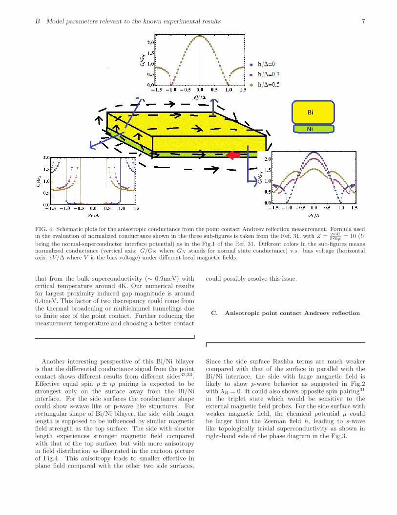
FIG. 4: Schematic plots for the anisotropic conductance from the point contact Andreev reflection measurement. Formula usedin the evaluation of normalized conductance shown in the three sub-figures is taken from the Ref. 31, with Z = 2mU
~2kF= 10 (U
being the normal-superconductor interface potential) as in the Fig.1 of the Ref. 31. Different colors in the sub-figures meansnormalized conductance (vertical axis: G/GN where GN stands for normal state conductance) v.s. bias voltage (horizontalaxis: eV/∆ where V is the bias voltage) under different local magnetic fields.
that from the bulk superconductivity (∼ 0.9meV) withcritical temperature around 4K. Our numerical resultsfor largest proximity induced gap magnitude is around0.4meV. This factor of two discrepancy could come fromthe thermal broadening or multichannel tunnelings dueto finite size of the point contact. Further reducing themeasurement temperature and choosing a better contact
could possibly resolve this issue.
C. Anisotropic point contact Andreev reflection
Another interesting perspective of this Bi/Ni bilayeris that the differential conductance signal from the pointcontact shows different results from different sides32,33.Effective equal spin p ± ip pairing is expected to bestrongest only on the surface away from the Bi/Niinterface. For the side surfaces the conductance shapecould show s-wave like or p-wave like structures. Forrectangular shape of Bi/Ni bilayer, the side with longerlength is supposed to be influenced by similar magneticfield strength as the top surface. The side with shorterlength experiences stronger magnetic field comparedwith that of the top surface, but with more anisotropyin field distribution as illustrated in the cartoon pictureof Fig.4. This anisotropy leads to smaller effective inplane field compared with the other two side surfaces.
Since the side surface Rashba terms are much weakercompared with that of the surface in parallel with theBi/Ni interface, the side with large magnetic field islikely to show p-wave behavior as suggested in Fig.2with λR = 0. It could also shows opposite spin pairing31
in the triplet state which would be sensitive to theexternal magnetic field probes. For the side surface withweaker magnetic field, the chemical potential µ couldbe larger than the Zeeman field h, leading to s-wavelike topologically trivial superconductivity as shown inright-hand side of the phase diagram in the Fig.3.

D Competing models and other possibilities 8
D. Competing models and other possibilities
Recent optical measurements of the polar Kerr effectsupports the spontaneous time reversal symmetrybreaking on the Bi surface in concurrence with theonset of superconductivity in this Bi/Ni bilayer34. Thisexperimental results are consistent with the time reversalbroken p ± ip paring gap presented in our theoreticalmodel. An alternative theoretical explanation forthe same Kerr effect results is presented in Ref. 34,where the superconductivity is thought to be occurringonly on the Bi surface away from the Bi/Ni interface.Based on symmetry requirements for two dimensionalnoncentrosymmetric crystalline superconductor35, theauthors in Ref. 34 concluded that the time reversalbroken superconducting state should be of d± id insteadof p ± ip as suggested in our scenario. The mechanismbehind this d ± id superconductivity is the magneticfluctuations induced by the Ni layer.
The key difference between this d ± id proposal andours is that the superconductivity considered in ourmodel is rooted from the bulk of Bi, not just on thesurface away from the Bi/Ni interface. It is true thatwith the decrease of Bi thickness the bulk of Bi tends tobe a normal insulator with metallic surface state24 (withthe exception of few bilayers of Bi which could be topo-logical insulator36 or single layer of Bi as two dimensionaltopological insulator37). However, by placing Bi on topof Ni thin film, we see the whole Bi/Ni normal statebehaves like an usual metal rather than an insulator.This leads us to believe that, in all the Bi/Ni samples wesee, there exist effective doping of charges which increasethe electronic density of state nearby the Fermi level.Also all the observed transport and magnetic properties,other than the surface probes such as the point contactAndreev reflection, in the superconducting state isconsistent with the usual type II s-wave superconductor.Another experimental support is that we do not seeany sign of superconductivity in the Bi/Fe or Bi/Cosamples14, which should have similar superconductingbehavior if the surface d ± id superconductivity wereinduced by magnetic fluctuations.
It is also possible that the observed p-wave like signalin the point contact measurement is from the bulk ofBi/Ni bilayer33 instead of signals from the surface. Itis found by T. Herrmannsdorfer et. al.38 that nano-structures of Bi3Ni (submicrometer-sized particles andquasi-one-dimensional nanoscaled strains) also showscoexistence of superconductivity and ferromagnetismwith onset superconducitng transition temperaturearound 5.2K. This kind of nano-structured Bi3Ni couldalso be formed during the epitaxial growth of Bi/Nibilayer and becomes the source of the bulk p-wavesuperconductivity, although the mechanism behind itremains elusive. Whether these nanostructured Bi3Nicould form well-oriented domains as suggested by the
anisotropy measurement32,33 during the epitaxial growthis yet another puzzle to be clarified.
Another possibility for seeing magnetic field indepen-dent zero bias conductance peak in the point contact An-dreev reflection measurement is that the point contact isnot in the Sharvin ballistic limit39. This has been seenin some of the multibands iron-pnictide superconductorswith s± pairing symmetry. In the polycrystalline iron-pnictide it is also found39 the coexistence of randomlydistributed ferromagnetic and superconducting domains.Both the field independent zero bias conductance peakand the existence of ferromagnetic domains could possi-bly explain the experimental results from the point con-tact and magneto-Kerr effect measurements found in theBi/Ni samples. This less exciting possibility can be ruledout, if the superconducting site found in the point con-tact measurement were the same as the ferromagneticregion found in the Kerr effect measurement. MultipleAndreev reflections40 is yet another possibility, althoughthe experimental results from Ref. 9 suggests this is lesslikely to be the case.
IV. SUMMARY AND FURTHEREXPERIMENTAL SUGGESTIONS
We propose a simple model, utilizing the strongspin orbit coupling nature of Bi and the effectivedoping coming from the alloy formation in the Bi/Nibilayer, to suggest the possible existence of proximityinduced time reversal broken p ± ip superconductivityon the Bi surface away from the Bi/Ni interface. Thephysics behind it is the same as the effective p ± ipsuperconductivity made by conventional superconductorcombined with a semiconductor with strong spin orbitcouplings under some external magnetic field17,18. Thekey difference here is the Rashba spin orbit term issupplemented by a cubic spin orbit coupling, and theexternal magnetic field is provided by the ferromagneticNi layer. By mapping out the phase diagram withexperimentally relevant parameters, we also explainthe anisotropic Andreev reflection signals probed ondifferent Bi surface32,33. This p± ip scenario is also con-sistent with the recent magneto-optical Kerr effect andmagnetic measurements21,34, although other possibilitiessuch as bulk p-wave superconductivity induced bynanostructured Bi3Ni
38, Multiple Andreev reflections40,or point contact in the diffusive regime39 should alsobe considered. Since the alloy formations would varywith growth methods, the phase diagrams mentionedin our simple model for the actual bilayer system issurely more complicated. However, we think the mainphysics that the topological nontrivial superconductivityis induced through proximity effect on the surface ofBi should be still the same, as long as the surfacestate of Bi away from the interface is not destroyed af-ter the formation of those alloys from interface diffusions.

9
To truly confirm whether our proposed scheme iscorrect or not, further surface probes such as Angleresolved photo emission spectroscopy or low temperaturescanning tunneling microscope is needed to check thenormal and superconducting state of electronic struc-tures of Bi layer after forming the Bi/Ni bilayer. Forsufficient thick Bi layer, the nickel from the interfacediffusion shall not reach to the Bi surface away fromthe interface. The size of the superconducting gap fromthe point contact Andreev reflection measurement shallbecome smaller with the increasing bismuth thickness.
Another possible mechanism for inducing time rever-sal broken superconductivity is through the magneticfluctuations from the Ni layer as mentioned in theRef. 34. We tend to exclude this scenario based onthe lack of superconductivity in the Bi/Fe and Bi/Cobilayers. Had it indeed been able to achieve effectivep ± ip superconductivity on the Bi surface, we mayadjust the sample makings processes to have the largestsuperconducting gap magnitude, using aforementionedphase diagrams, and make Majorana zero modes in itsvortex state. Even if it were not the cases (say, with zerobias anomaly seen similar to some of the iron-pnictidesuperconductors), a further look at the Fulde FerrellLarkin Ovchinnikov (FFLO) physics on the Ni side11 isalso an interesting topic in its own right. A systematicstudy of bilayer formed by metallic/semi-conductingthin film with strong spin orbit couplings and ferromag-netic metal/insulator layer could also possibly leads tothe platform for effective p ± ip or even more exoticsuperconductors yet to be explored.
Acknowledgments
I acknowledge useful discussions with Piers Colemanin the initial stage of this work, and various discussionswith friends from Institute of Physics, Academia Sinicaduring the writeup of this work. I also thank thefinancial support from Taiwan’s MOST (No.106-2112-M-017-002-MY3), NSF funding from U.S.A. for the Aspencenter for physics 2017 winter conference, and AcademiaSinica during my winter and summer visits in 2016-2017.
Appendix A: Overview of Sau-Lutchyn-Tewari-DasSarmar proposal
The mechanism for generating p±ip superconductivityin this paper follows the idea pioneered by Sau et. al. inthe Ref. 17, of utilizing semiconductors with strong spinorbit coupling under external magnetic field and placedin close contact with a conventional superconductor. Wesummarize their main formulations and results following
the review article41 and paper18 by Jason Alicea.
The proposed setup for realizing p ± ip supercon-ductivity is to use a semiconductor quantum well(a quasi two dimensional electron gas (2DEG)) withstrong Rashba spin orbit coupling placed in betweena conventional s-wave superconductor and a ferromag-netic insulator. The magnetization direction of theferromagnetic insulator is pointing perpendicular tothe plane of the two dimensional electron gas formedin the quantum well. This stacking order (s wavesuperonductor-2DEG-Ferromagnetic insulator) is differ-ent from the scenario for Bi/Ni bilayer (2DEG-s wavesuperonductor-Ferromagnetic metal) we mentioned inthe main text. The direction of magnetization and thespin orbit coupling terms for generating topologicalsuperconductivity is slightly different in our proposal. Inthe following, we introduce term by term the low energyHamiltonian describing the setup by Sau at. al.17, start-ing with the 2DEG with Rashba spin orbit coupling part.
Up to quadratic order in momentum, the relevantHamiltonian for the electrons in the quantum well is:
Ho =
∫
d2rψ†
[
−∇2
2m− µ− iα(σx∂y − σy∂x)
]
ψ (A1)
where m is the effective mass, µ is the chemical po-tential, α is the Rashba spin-orbit coupling strength,and σi are Pauli matrices acting on the spin degree offreedom in ψ. At small enough momentum (around Γpoint in the reciprocal lattice) the Rashba term in theEq.(A1) gives spin-orbit coupled band similar to theelectrons of the two dimensional surface state of a threedimensional topological insulator. The emergence ofp± ip superconductivity is closely related to this term.
Next the coupling with a ferromagnetic insulator withmagnetization pointing out of plane is assumed to inducea Zeeman interaction:
HZ =
∫
d2rψ†[hzσz ]ψ (A2)
Under the assumption that the influence from the fer-romagnetic insulator were primarily due to exchange in-teraction, this Zeeman interaction is the dominant term.For |hz| > |µ| the electrons occupy only the lower bandand exhibit a single Fermi surface. To see this we maydiagonalize H0 +HZ in momentum space by writing
ψ(~k) = φ−(~k)ψ−(~k) + φ+(~k)ψ+(~k) (A3)
where ψ±(~k) are the fermion annihilation operators for
upper/lower bands, and φ±(~k) are the corresponding

10
wave functions taking the following form:
φ+(~k) =
(
A↑(~k)
A↓(~k)ikx−ky
|~k|
)
, (A4)
φ−(~k) =
(
B↑(~k)ikx+ky
|~k|
B↓(~k)
)
. (A5)
The expression for A↑,↓ and B↑,↓ are not thatenlightening18, but the combination of them as shownbelow are more meaningful:
fp(~k) ≡ A↑A↓ = B↑B↓ =−α|~k|
2
√
h2z + α2|~k|2, (A6)
fs(~k) ≡ A↑B↓ −B↑A↓ =hz
√
h2z + α2|~k|2. (A7)
Eq.(A6) and Eq.(A7) are useful for identifying the for-mation of p± ip and s-wave superconductivity once theproximity induced pairing is introduced. In this bandbases, H0 +HZ becomes:
H0 +HZ =
∫
d~k[
ǫ+(~k)ψ†+(~k)ψ+(~k) + ǫ−(~k)ψ
†−(~k)ψ−(~k)
]
with energies
ǫ±(~k) =|~k|22m
− µ±√
h2z + α2|~k|2.
Making this 2DEG in contact with a s-wave supercon-ductor introduces a pairing term via the proximity effect.The full Hamiltonian is given by:
H = H0 +HZ +HSc (A8)
with
HSc =
∫
d2r[
∆ψ†↑ψ
†↓ +∆∗ψ↓ψ↑
]
. (A9)
We choose ∆ = ∆∗ in this s-wave pairing. Rewriting HSc
in terms of band bases ψ± in momentum space we get:
HSc =
∫
d~k[
∆+−(~k)ψ†+(~k)ψ†
−(−~k) + ∆++(~k)
×ψ†+(~k)ψ†
+(−~k) + ∆−−(~k)ψ†−(~k)ψ†
−(−~k) + h.c.]
with
∆+−(~k) = fs(~k)∆, (A10)
∆++(~k) = fp(~k)
(
ky + ikx
|~k|
)
∆, (A11)
∆−−(~k) = fp(~k)
(
ky − ikx
|~k|
)
∆. (A12)
In this band basis we see that Eq.(A9) generates bothinterband s-wave paring ∆+− and intraband p ± ippairing for upper/lower bands. This mixing pairings isdue to spin-momentum locking from the Rashba spinorbit coupling. For proximity effect induced pairingamplitude ∆ much smaller than the band gap inducedby the Zeeman field (i.e. |hz − µ| ≫ ∆) with µ crossingthe lower band, we can ignore the upper band andproject ψ+ away from the effective Hamiltonian. Thenthe remaining effective Hamiltonian maps onto thatof spinless p − ip pairing, an example of topologicalsuperconductor. Notice that even in this topologicalsuperconducting regime the interband s-wave paring∆+− is still nonzero around Γ point in reciprocal space.The reason for projecting interband pairing away ispurely due to the energetic assumption that |hz−µ| ≫ ∆.
To explore the stability conditions at zero temperaturefor this topological superconducting phase, we solve thefull Hamiltonian Eq.(A8) and obtain:
E2± = 4|∆++|2 +∆2
+− +ǫ2+ + ǫ2−
2
±|ǫ+ − ǫ−|√
∆2+− +
(ǫ+ − ǫ−)2
4. (A13)
For the lower band energy eigenvalue E−(~k) the super-conducting pairing amplitude is obtained at the Fermi
momentum kF (obtained from ǫ−(~kF ) = 0). The small-
est E−(~k) band gap is around ~k = 0 (the Γ point in
reciprocal space). This gap closing (E−(~k) = 0 at some~k close to Γ point, named ”gapless superconducting” re-gion in the Fig.2,3 of the main text) marks the transitionfrom topological superconducting phase (absolute valueof Chern number equals to one) to trivial (normal) su-perconducting phase (Chern number equals to zero)41.
1 N. Read and D. Green, Phys. Rev. B 61, 10267 (2000).2 A. Kitaev, Phys. Usp. 44, 131 (2001).3 S. S. Saxena, P. Agarwal, K. Ahilan, F. M. Grosche,R. K. W. Haselwimmer, M. J. Steiner, E. Pugh, I. R.Walker, S. R. Julian, P. Monthoux, G. G. Lonzarich,A. Huxley, I. Sheikin, D. Braithwaite, and J. Flouquet,Nature 406, 587 (2000).
4 D. Aoki, A. Huxley, E. Ressouche, D. Braithwaite, J. Flou-quet, J.-P. Brison, E. Lhotel, and C. Paulsen, Nature 413,613 (2001).
5 N. T. Huy, A. Gasparini, D. E. de Nijs, Y. Huang, J. C. P.Klaasse, T. Gortenmulder, A. de Visser, A. Hamann,T. Gorlach, and H. v. Lohneysen, Phys. Rev. Lett. 99,067006 (2007).

11
6 F. S. Bergeret, A. F. Volkov, and K. B. Efetov, Phys. Rev.Lett. 86, 4096 (2001).
7 A. Kadigrobov, R. I. Shekhter, and M. Jonson, Euro-physics Letters 54 (3), 394 (2001).
8 K. T. Law, P. A. Lee, and T. K. Ng, Phys. Rev. Lett. 103,237001 (2009).
9 X.-X. Gong, He-Xin, Z. P.-C. Xu, D. Yue, K. Zhu, X.-F.Jin, H. Tian, and G.-J. Zhao, Chinese Physics Letter 32,067402 (2015).
10 J. S. Moodera and R. Meservey, Phys. Rev. B 42, 179(1990).
11 P. LeClair, J. S. Moodera, J. Philip, and D. Heiman, Phys.Rev. Lett 94, 037006 (2005).
12 O. Prakash, A. Kumar, A. Thamizhavel, and S. Ramakr-ishnan, Science 355, 52 (2017).
13 V. Siva, K. Senapati, B. Satpati, S. Prusty, D. K. Avasthi,D. Kanjilal, and P. K. Sahoo, Journal of Applied Physics117, 083902 (2015).
14 S. Chao, S. C. Lu, J. H. Lin, P. Chiu, W. J. Li, P. J. Chen,Y. Liou, and T. K. Lee, APS March Meeting 2017 62,R45.00006 (2017).
15 L. Y. Liu, Y. T. Xing, I. L. C. Merino, H. Micklitz, D. F.Franceschini, E. Baggio-Saitovitch, D. C. Bell, and I. G.Solorzano, Phys. Rev. Materials. 2, 014601 (2018).
16 J. Kumar, A. Kumar, A. Vajpayee, B. Gahtori, D. Sharma,P. K. Ahluwalia, S. Auluck, and V. P. S. Awana, Super-cond. Sci. Technol. 24, 085002 (2011).
17 J. D. Sau, R. M. Lutchyn, S. Tewari, and S. DasSarma,Phys. Rev. Lett. 104, 040502 (2010).
18 J. Alicea, Phys. Rev.B 81, 125318 (2010).19 L. Fu and C. L. Kane, Phys. Rev. Lett. 100, 096407 (2008).20 J. A. van Hulst, G. Rietveld, D. van der Marel, F. Tuinstra,
and H. M. Jaeger, Phys. Rev. B 47, 548 (1993).21 H. Zhou, X. Gong, and X. Jin, Journal of Magnetism and
Magnetic Materials 422, 73 (2017).22 G. J. Zhao, X. X. Gong, P. C. Xu, B. C. Li, Z. Y. Huang,
X. F. Jin, X. D. Zhu, and T. Y. Chen, arXiv: 1805.09811(2018).
23 P. Chauhan, F. Mahmood, D. Yue, P.-C. Xu, X. Jin, andN. Armitage, Phys. Rev. Lett. 122, 017002 (2019).
24 S. Xiao, D. Wei, and X. Jin, Phys. Rev. Lett. 109, 166805(2012).
25 Y. M. Koroteev, G. Bihlmayer, J. E. Gayone, E. V.Chulkov, S. Blugel, P. M. Echenique, and P. Hofmann,Phys. Rev. Lett. 93, 046403 (2004).
26 T. Hirahara, T. Nagao, I. Matsuda, G. Bihlmayer, E. V.Chulkov, Y. M. Koroteev, P. M. Echenique, M. Saito, andS. Hasegawa, Phys. Rev. Lett. 97, 146803 (2006).
27 K. Saito, H. Sawahata, T. Komine, and T. Aono, Phys.Rev. B 93, 041301(R) (2016).
28 Y. M. Koroteev, G. Bihlmayer, E. V. Chulkov, andS. Blugel, Phys. Rev. B. 77, 045428 (2008).
29 T. Hirahara, K. Miyamoto, I. Matsuda, T. Kadono,A. Kimura, T. Nagao, G. Bihlmayer, E. V. Chulkov,S. Qiao, K. Shimada, H. Namatame, M. Taniguchi, andS. Hasegawa, Phys. Rev. B. 76, 153305 (2007).
30 J. I. Pascual, G. Bihlmayer, Y. M. Koroteev, H.-P. Rust,G. Ceballos, M. Hansmann, K. Horn, E. V. Chulkov,S. Blugel, P. M. Echenique, and P. Hofmann, Phys. Rev.Lett. 93, 196802 (2004).
31 T. Yokoyama and Y. Tanaka, Phys. Rev. B 75, 132503(2007).
32 X. Jin, talk given in a seminar at Institute of Physics,Academia Sinica, Taiwan. (2016).
33 C. L. Chien, talk titled ”Triplet p-wave superconductivitywith ABM state in Bi/Ni bilayers” given in the Instituteof Physics, Academia Sinica, Taiwan. (2018).
34 X. Gong, M. Kargarian, A. Stern, D. Yue, H. Zhou, X. Jin,V. M. Galitski, V. M. Yakovenko, and J. Xia, ScienceAdvances 3, e1602579 (2017).
35 K. V. Samokhin, Phys. Rev. B 92, 174517 (2015).36 S. Ito, B. Feng, M. Arita, A. Takayama, R.-Y. Liu,
T. Someya, W.-C. Chen, T. Iimori, H. Namatame,M. Taniguchi, C.-M. Cheng, S.-J. Tang, F. Komori,K. Kobayashi, T.-C. Chiang, and I. Matsuda, Phys. Rev.Lett. 117, 236402 (2016).
37 Z. Liu, C.-X. Liu, Y.-S. Wu, W.-H. Duan, F. Liu, andJ. Wu, Phys. Rev. Lett. 107, 136805 (2011).
38 T. Herrmannsdorfer, R. Skrotzki, J. Wosnitza, D. Kohler,R. Boldt, and M. Ruck, Phys. Rev. B 83, 140501(R)(2011).
39 X. Lu, W. K. Park, H. Q. Yuan, G. F. Chen, G. L. Luo,N. L. Wang, A. S. Sefat, M. A. McGuire, R. Jin, B. C.Sales, D. Mandrus, J. Gillett, S. E. Sebastian, and L. H.Greene, Supercond. Sci. Technol. 23, 054009 (2010).
40 P. Parab, P. Chauhan, H. Muthurajan, and S. Bose, J.Phys.: Condens. Matter 29, 135901 (2017).
41 J. Alicea, Rep. Prog. Phys. 75, 076501 (2012).