supporting information · molecule-passivated ruddlesden-popper/3d heterostructured film ......
TRANSCRIPT

Supporting information
High performance ambient-air-stable FAPbI3 perovskite solar cells with molecule-passivated Ruddlesden-Popper/3D heterostructured film
Tianqi Niu,‡a Jing Lu,‡a Ming-Chun Tang,b Dounya Barrit,b Detlef-M. Smilgies,c Zhou Yang, a Jianbo Li,a Yuanyuan Fan,a Tao Luo,a Iain McCulloch,b Aram Amassian,*b Shengzhong (Frank) Liu*ad and Kui Zhao*a
a Key Laboratory of Applied Surface and Colloid Chemistry, Ministry of Education; Shaanxi Key Laboratory for
Advanced Energy Devices; Shaanxi Engineering Lab for Advanced Energy Technology, School of Materials
Science and Engineering, Shaanxi Normal University, Xi’an 710119, China. Email: [email protected] King Abdullah University of Science and Technology (KAUST), KAUST Solar Center (KSC) and Physical
Science and Engineering Division (PSE), Thuwal 23955-6900, Saudi Arabia.
Email: [email protected] c Cornell High Energy Synchrotron Source, Cornell University, Ithaca, NY 14850, USA.d Dalian National Laboratory for Clean Energy; iChEM, Dalian Institute of Chemical Physics, Chinese Academy
of Sciences, Dalian, 116023, China. Email: [email protected]
‡ T.N. and J.L. contributed equally.
Corresponding author: [email protected]; [email protected]; [email protected]
Electronic Supplementary Material (ESI) for Energy & Environmental Science.This journal is © The Royal Society of Chemistry 2018
Experimental Section
Solution preparation and device fabrication
Materials preparation: Lead iodide (PbI2, 99.9985%) was purchased from AlfaAesar.
Formamidine iodide (FAI), Butylamine iodide (BAI), Butylammonium Bromide
(BABr), Butylammonium Chloride (BACl), Lead(II) bromide (PbBr2, 99.99%) and
Lead(II) chloride (PbCl2, 99.99%) were purchased from p-OLED. N,N-
dimethylformamide (DMF, 99.8%), dimethylsulfoxide (DMSO, 99.9%) and γ-
butyrolactone (GBL, 99%) were purchased from Sigma-Aldrich. ITIC and IDTBR
were purchased from One-material. All chemicals were used as received without
further purification.
Solution preparation: The precursor solution preparation was conducted under inert
atmosphere inside a nitrogen glove box. The FAPbI3 precursor solution (1.2M) was
prepared with equimolar PbI2 and Formamidine iodide (FAI) dissolved in a mixture of
dimethylsulfoxide (DMSO), γ-butyrolactone (GBL) and N,N-dimethylformamide
(DMF) (volume ratio of 7:7:6) in a glovebox. To form a quasi-2D perovskite solution
(1.2M), BAX, FAI, PbX2 and PbI2 (X denotes halogen) were mixed with the ratio of
2:60:1:60 and dissolved in the same solvent recipe as FAPbI3. All solutions were
filtered prior to solution-casting. ITIC and IDTBR solutions were resolved in
chlorobenzene with the concentration of 0.4 mg/ml. The Spiro-OMeTAD solution
was prepared by dissolving 90 mg Spiro-OMeTAD, 22 μL lithium
bis(trifluoromethanesulfonyl) imide in acetonitrile and 36 μL 4-tert-butylpyridine in 1
mL chlorobenzene.

Device fabrication: The FTO-coated glass (2.5 cm * 2.5 cm) was cleaned by
sequential sonication in acetone, isopropanol and ethanol for 30 min each and then
dried under N2 flow and treated by O3 plasma for 15 min. The TiO2 was prepared by
chemical bath deposition with the clean substrate immersed in a TiCl4 (CP,
Sinopharm Chemical Reagent Co., Ltd) aqueous solution with the volume ratio of
TiCl4 : H2O equal to 0.0225 : 1 at 70 °C for 1 hour. The spin-coating was
accomplished under inert atmosphere inside a nitrogen glove box. The procedure was
performed at 1000 r.p.m. for 10 s followed by 4000 r.p.m. for 40 s. At ca. 25 s before
the end of the last spin-coating step, 100 μL of chlorobenzene solvent or loaded
solution was dropped onto the substrate. The substrates were then placed onto a
hotplate for 30 min at 150 °C. Subsequently, the HTM were deposited on top of the
perovskite by spin coating at 5000 r.p.m. for 30 s followed by evaporation of 100 nm
gold electrode on the top of the cell.
Characterization
Optical metrology: UV-Visible absorption spectra were acquired on a PerkinElmer
UV-Lambda 950 instrument. Steady-state Photoluminescence (PL) (excitation at 510
nm) was measured with an Edinburgh Instruments Ltd (FLS980 spectrometer).
Electronic microscopy: The surface morphology and structure of the perovskite films
were characterized by SEM (FE-SEM; SU-8020, Hitachi) and Atomic force
microscopy (AFM, Dimension ICON), respectively.

X-ray diffraction (XRD) measurements were carried out in a θ-2θ configuration with
a scanning interval of 2θ between 5 and 60 on a Rigaku Smart Lab (X-ray Source:
Cu Kα; = 1.54 Å).
Grazing incidence wide angle X-ray scattering (GIWAXS) measurements were
performed at D-line at the Cornell High Energy Synchrotron Source (CHESS). The
wavelength of the X-rays was 0.972 Å with a bandwidth ∆λ/λ of 1.5%. The scattering
signal was collected by a Pilatus 200K detector, with a pixel size of 172 µm by 172
µm placed 184.0066 mm away from the sample position. The incident angle of the X-
ray beam was 0.35 degree. Spin-coating experiments were conducted at a custom-
built spin-coating stage with splashing of solvent protected using kapton tape and
controlled from a computer outside the hutch. The exposure time was kept at 0.5 s to
obtain the detailed information of the process.
UPS measurements: Ultraviolet photoelectron spectroscopy (UPS) was measured
with a monochromatic He I light source (21.22 eV) and a VG Scienta R4000 analyzer.
Solar cell characterizations: The J-V performance of the perovskite solar cells was
measured using a Keithley 2400 source-meter under ambient condition at room
temperature, and the illumination intensity was 100 mW cm-2 (AM 1.5G Oriel solar
simulator). The scan rate was 0.3 V s-1. The delay time was 10 ms; and the scan step
was 0.02 V. The power output of the lamp was calibrated by a NREL-traceable KG5-
filtered silicon reference cell. The device area of 0.09 cm2 was defined by a metal
aperture to avoid light scattering from the metal electrode onto the device during the
measurement. The EQE was characterized on a QTest Station 2000ADI system
(Crowntech. Inc., USA), and the light source was a 300 W xenon lamp. The
monochromatic light intensity for EQE measurements was calibrated with a reference
silicon photodiode.
Mobility measurement: Electron-only devices (FTO/c-TiO2/perovskites/PCBM/Ag)
were fabricated to measure the electron mobility of the devices. The dark J-V
characteristics of the electron-only devices were measured by a Keithley 2400
sourcemeter. The mobility was extracted by fitting the J-V curves with the Mott-
Gurney equation. The trap state density was determined by the trap-filled limit
voltage using equation 2.
Electrical impedance spectroscopy (EIS) measurement: Electrical impedance
spectroscopy (EIS) measurements were conducted using an electrochemical
workstation (IM6ex, Zahner, Germany) with the frequency range from 10 Hz to 4
MHz at open-circuit voltage in the dark.
Contact angle measurements were conducted on a Dataphysics OCA-20 with a drop
of ultrapure water (0.05 mL). The photographs were taken 1 second after water
dripping.

(FAPbI3)n(BA2PbX4) (FAPbI3)n(BA2PbX4)
Dripping ITIC or IDTBR loaded solution
NCCN
S
S
S
S
C6H13 C6H13
C6H13 C6H13
O
O
CN
NC
ITIC
S
SNS N
SN
O
S
NSN
SN
O
S
IDTBR
(a)
(b)
Fig. S1. (a) Molecular structure of the selected semiconducting molecules with Lewis base functional groups. (b) Schematic diagram of loaded anti-solvent dripping strategy for fabricating RP/3D heterostructured perovskite films.
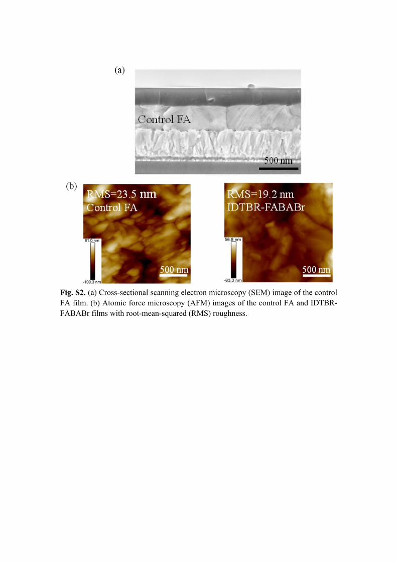
Fig. S2. (a) Cross-sectional scanning electron microscopy (SEM) image of the control FA film. (b) Atomic force microscopy (AFM) images of the control FA and IDTBR-FABABr films with root-mean-squared (RMS) roughness.
300 400 500 600 700 8000
20
40
60
80
100
Wavelength (nm)
Control FA IDTBR- FABABr 0
4
8
12
16
20
24
Integrated Jsc (m
A cm-2)
EQE
(%)
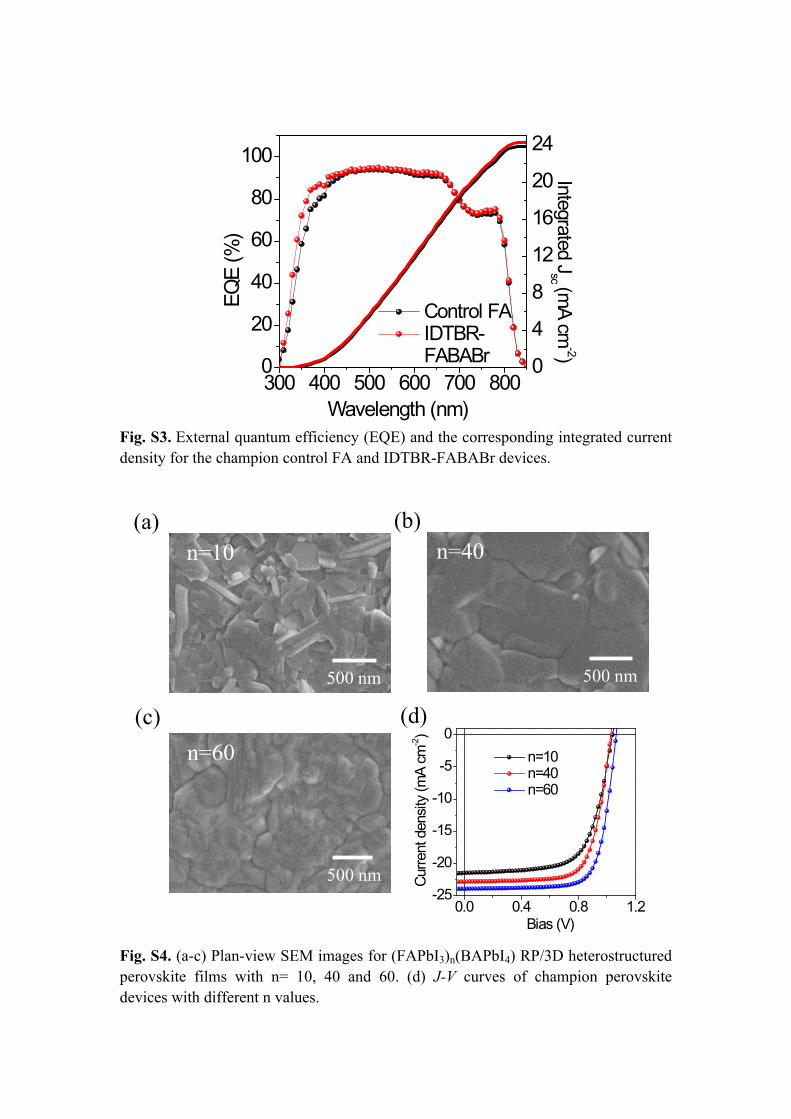
Fig. S3. External quantum efficiency (EQE) and the corresponding integrated current density for the champion control FA and IDTBR-FABABr devices.
n=10
500 nm
n=40
500 nm
(a) (b)
0.0 0.4 0.8 1.2-25
-20
-15
-10
-5
0
Bias (V)
Curre
nt d
ensit
y (m
A cm
-2)
n=10 n=40 n=60
(c) (d)
500 nm
n=60
Fig. S4. (a-c) Plan-view SEM images for (FAPbI3)n(BAPbI4) RP/3D heterostructured perovskite films with n= 10, 40 and 60. (d) J-V curves of champion perovskite devices with different n values.
-25 -20 -15 -10 -5 0
5
10
15
20
25
q z (n
m-1)
qxy (nm-1)-25 -20 -15 -10 -5 0
5
10
15
20
25
q z (n
m-1)
qxy (nm-1)
-25 -20 -15 -10 -5 0
5
10
15
20
25
q z (n
m-1)
qxy (nm-1)
FABACl
FABAI
FABABr
-25 -20 -15 -10 -5 0
5
10
15
20
25q z
(nm
-1)
qxy (nm-1)
Control FA(a) (b)
(c) (d)
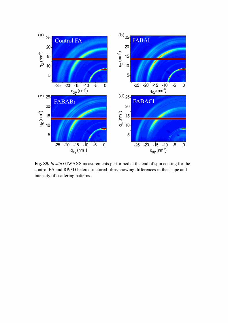
Fig. S5. In situ GIWAXS measurements performed at the end of spin coating for the control FA and RP/3D heterostructured films showing differences in the shape and intensity of scattering patterns.

500 nm
RMS=15.6 nm RMS=20.7 nm
RMS=20.7 nmRMS=24.0nm RMS=21.2 nm
500 nm 500 nm 500 nm
500 nm
FABACl
FABAI FABABr FABACl
(a) (b)
(c)
500 nm
FABABr
Fig. S6. (a-b) Plan-view SEM images of FABABr and FABACl films. (c) AFM images of the RP/3D heterostructured perovskite films with root-mean-squared (RMS) roughness.
FABAI FABACl
-25 -20 -15 -10 -5 0
5
10
15
20
q z (n
m-1)
qxy (nm-1)
Control FA
-25 -20 -15 -10 -5 0
5
10
15
20
q z (n
m-1)
qxy (nm-1)-25 -20 -15 -10 -5 0
5
10
15
20
q z (n
m-1)
qxy (nm-1)
(a) (b) (c)
Fig. S7. Ex situ GIWAXS patterns of the control FA, FABAI and FABACl films.
1.5 1.6 1.7
hv (eV)
FABABr
1.54
1.5 1.6 1.70.00
0.02
0.04
0.06
0.08
0.10
hv (eV)
(F(R
)hv)
2
1.53
Control FA
1.5 1.6 1.7
hv (eV)
FABACl
1.55
1.5 1.6 1.7
1.53
FABAI
hv (eV)
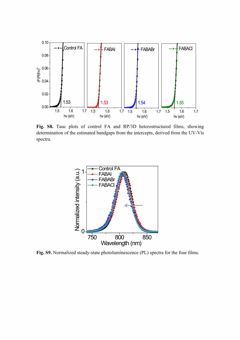
Fig. S8. Tauc plots of control FA and RP/3D heterostructured films, showing determination of the estimated bandgaps from the intercepts, derived from the UV-Vis spectra.
750 800 8500
1 Control FA FABAI FABABr FABACl
Wavelength (nm)
Norm
alize
d in
tens
ity (a
.u.)
Fig. S9. Normalized steady-state photoluminescence (PL) spectra for the four films.

0.01 0.1 11E-6
1E-5
1E-4
1E-3
0.01
0.1
1
Voltage (V)
FABABr
electron=3.56 cm2V-1S-1ntrap=1.18*1016 cm-3
VTFL=0.21V
Curre
nt (A
)
0.01 0.1 1
1E-6
1E-5
1E-4
1E-3
0.01
0.1
1
electron=4.23 cm2V-1S-1ntrap=8.44*1015 cm-3
VTFL=0.15V
Voltage (V)
Curre
nt (A
) Control FA
0.01 0.1 1
1E-3
0.01
0.1
1
electron=3.76 cm2V-1S-1
Curre
nt (A
)
Voltage (V)
ntrap=6.18*1015 cm-3
VTFL=0.11V
FABAI
0.01 0.1 1
1E-4
1E-3
0.01
0.1
electron=1.88 cm2V-1S-1
ntrap=1.41*1016 cm-3Curre
nt (A
)
Voltage (V)
FABACl
VTFL=0.25V
Fig. S10. Dark I-V measurement data of the electron-only devices with the architecture FTO/TiO2/perovskite/PCBM/Ag for the four cases displaying VTFL kink point behavior.
300 400 500 600 700 8000
20
40
60
80
100
FABAI FABABr FABACl
0
4
8
12
16
20
24
Wavelength (nm)
EQE
(%)
Integrated Jsc (m
A cm-2)
0.0 0.4 0.8 1.2-25
-20
-15
-10
-5
0
Bias (V)
Curre
nt d
ensit
y (m
A cm
-2)
FABAI FABABr FABACl
(a) (b)
Fig. S11. (a) J-V curves for champion devices based on RP/3D heterostructured films. (b) EQE and the corresponding integrated current density for the three cases.

0 100 200 3000
5
10
15
20
25
Curre
nt d
ensit
y (m
A cm
-2)
PCE (%)
Time (sec)
FABACl
0
5
10
15
20
25
Jsc=20.26 mA/cm2
Vmax=0.86VPCE=17.42 %
0 100 200 3000
5
10
15
20
25
Time (sec)
PCE (%)
Curre
nt d
ensit
y (m
A cm
-2)
FABAI
Vmax=0.86V
0
5
10
15
20
25
PCE=18.73 %
Jsc=21.78 mA/cm2
0 100 200 3000
5
10
15
20
25
Time (sec)
Curre
nt d
ensit
y (m
A cm
-2)
Vmax=0.86V
FABABr
0
5
10
15
20
25
PCE (%)
PCE=18.69 %
Jsc=21.73 mA/cm2
Fig. S12. The stabilized power output of the champion devices based on the RP/3D heterostructured films measured at a fixed maximum power point (MPP) voltage as a function of time.
0.0 0.4 0.8 1.2-25
-20
-15
-10
-5
0
Curre
nt d
ensit
y (m
A cm
-2)
Bias (V)
FABACl Reverse
17.66% PCE Forward
15.95% PCE
0.0 0.4 0.8 1.2-25
-20
-15
-10
-5
0
Bias (V)
Curre
nt d
ensit
y (m
A cm
-2) FABAI
Reverse 18.82% PCE
Forward 18.03% PCE
0.0 0.4 0.8 1.2-25
-20
-15
-10
-5
0
Bias (V)
Curre
nt d
ensit
y (m
A cm
-2) FABABr
Reverse 18.76% PCE
Forward 17.95% PCE
Fig. S13. J-V curves recorded in both the reverse and forward scan directions for the RP/3D devices.
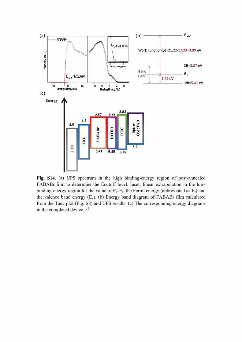
Fig. S14. (a) UPS spectrum in the high binding-energy region of post-annealed FABABr film to determine the Ecutoff level. Inset: linear extrapolation in the low-binding-energy region for the value of Ev-Ef, the Fermi energy (abbreviated as Ef) and the valence band energy (Ev). (b) Energy band diagram of FABABr film calculated from the Tauc plot (Fig. S8) and UPS results. (c) The corresponding energy diagrams in the completed device.1, 2

500 nm
ITIC-FABABr
500 nm
RMS=21.2 nm
ITIC-FABABr
(a) (b)
Fig. S15. (a) Plan-view SEM image of ITIC-FABABr films. (b) AFM image of ITIC-FABABr film with root-mean-squared (RMS) roughness.
500 600 700 800 9000
1
2
3 FABABr ITIC-FABABr IDTBR-FABABr
Wavelength (nm)
Abso
rban
ce (a
.u.)
Fig. S16. UV spectroscopy measurement for FABABr films with and without ITIC or IDTBR passivation layer on glass.
0 10 20 30 400
20
40
Z (o
hm)
Z (ohm)
FABABr ITIC-FABABr IDTBR-FABABr Fitting linear
Rs Rco
Cco Crec
Rrec
(a) (b)
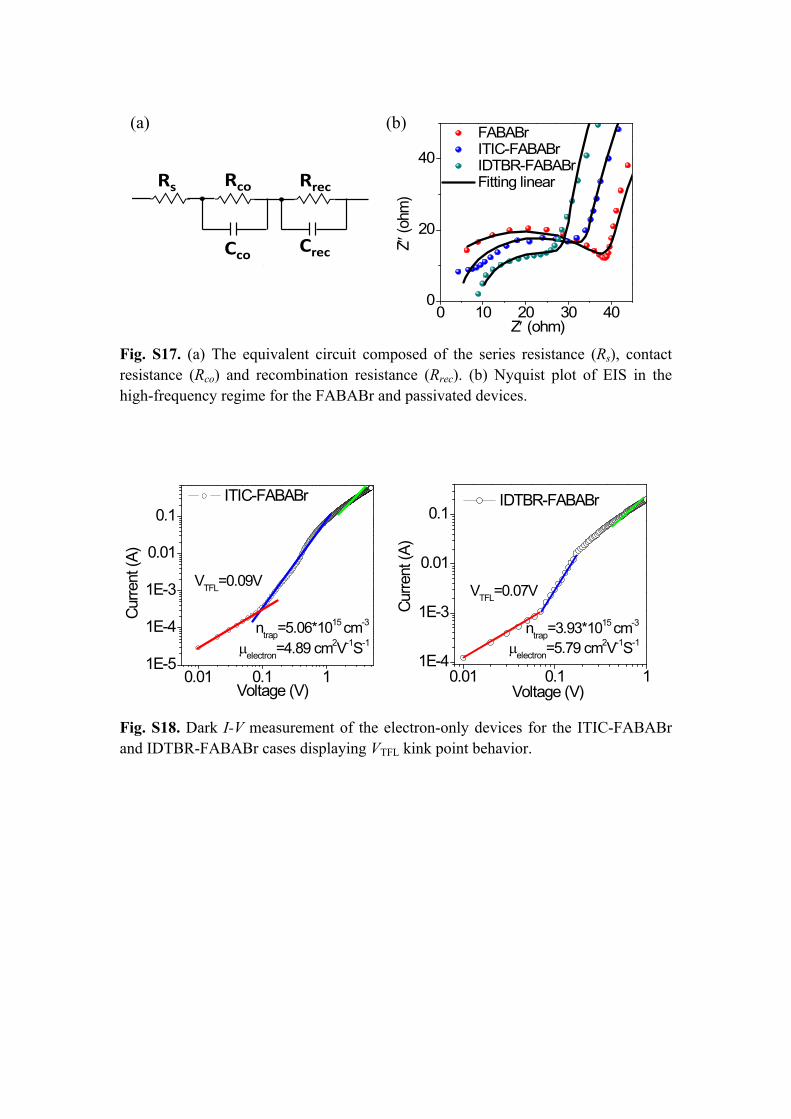
Fig. S17. (a) The equivalent circuit composed of the series resistance (Rs), contact resistance (Rco) and recombination resistance (Rrec). (b) Nyquist plot of EIS in the high-frequency regime for the FABABr and passivated devices.
0.01 0.1 11E-5
1E-4
1E-3
0.01
0.1
VTFL=0.09V
electron=4.89 cm2V-1S-1ntrap=5.06*1015 cm-3
Voltage (V)
Curre
nt (A
)
ITIC-FABABr
0.01 0.1 11E-4
1E-3
0.01
0.1
Voltage (V)
Curre
nt (A
)
IDTBR-FABABr
electron=5.79 cm2V-1S-1ntrap=3.93*1015 cm-3
VTFL=0.07V
Fig. S18. Dark I-V measurement of the electron-only devices for the ITIC-FABABr and IDTBR-FABABr cases displaying VTFL kink point behavior.

0 100 200 3000
5
10
15
20
25
Time (sec)
PCE (%)
Curre
nt d
ensit
y (m
A cm
-2)
ITIC-FABABr
Vmax=0.90V
0
5
10
15
20
25
PCE=20.01 %
Jsc=22.23 mA/cm2
0.0 0.4 0.8 1.2-25
-20
-15
-10
-5
0
Bias (V)
Curre
nt d
ensit
y (m
A cm
-2)
ITIC-FABABr Reverse
20.10% PCE Forward
19.19% PCE
(a) (b) (c)
300 400 500 600 700 8000
20
40
60
80
100
Wavelength (nm)
EQE
(%)
ITIC-FABABr
0
4
8
12
16
20
24Integrated J
sc (mA cm
-2)
Fig. S19. Characteristics of devices based on ITIC-FABABr film. (a) J-V curves recorded in both the reverse and forward scan directions. (b) The stabilized power output and (c) EQE of the champion device.
0 10 20 30 40 50 600.00.20.40.60.81.0
Time (days)
Norm
alize
d PC
E
Control FA FABAI FABABr FABACl
10 20 30 40 50 60 70 80
Inte
nsity
(a.u
.)
2degrees)
FABACl
FABABr
FABAI*Control FA
FABAIControl FA FABAClFABABr
10 days
60 days
FABAI
81.9°
Control FA
70.7° 83.1°
FABACl
82.8°
FABABr
(a)
(c)
(b)
(d)
Fig. S20. Long term environmental stability characterization. (a) Pictures of the control FA and RP/3D heterostructured perovskite films before and after aging under ambient conditions with 30-40% relative humidity at room temperature. (b) XRD patterns of the four cases before and after aging under ambient conditions with 30-40% relative humidity at room temperature. (c) Contact angle of water on different perovskite films showing increased hydrophobicity of the RP/3D films compared with the control film. (d) Long-term stability measurements of both solar cells without any encapsulation under ambient conditions with 30-40% relative humidity. After 60 d, the RP/3D FABAI, FABABr and FABACl fabricated devices exhibit significantly improved stability against humidity, maintaining 56.1%, 74.2% and 69.4% of their initial PCEs, respectively, in contrast to the control device at only 20.2% of initial PCE.

88.7°
IDTBR-FABABr
92.5°
ITIC-FABABr
0 10 20 30 40 50 60
0.6
0.8
1.0
Time (days)
Norm
alize
d PC
E
FABABr ITIC-FABABr IDTBR-FABABr
(a)
(b)
Fig. S21. (a) Contract angle of water on ITIC-FABABr and IDTBR-FABABr films. (b) Long-term stability measurements for the FABABr and passivated devices. For the ITIC passivated device, 90.1% of the initial PCE value was retained after 60 days, which is better than the value of FABABr at 74.2% and IDTBR passivated one at 87.3%.

0 20 40 60 80 100 120 1400.0
0.2
0.4
0.6
0.8
1.0
Time (h)
Norm
alize
d PC
E (%
)
Control FA FABABr ITIC-FABABr IDTBR-FABABr
Fig. S22. Operational Stability. The evolution of the PCEs for the non-encapsulated control FA,FABABr,ITIC-FABABr and IDTBR-FABABr devices exposed to continuous illumination (100 mW cm-2) under open-circuit condition in air (50-60% RH and 50 ºC). The ITIC-FABABr and IDTBR-FABABr based devices still maintained 72.6% and 68.9% of the initial values after 130h continuous illumination, respectively, which significantly outperform the control one.

Table S1. Photovoltaic parameters of devices based on the control FA and IDTBR-FABABr films.
VOC
(V)
JSC
(mA cm-2)FF(%)
PCE (%)
PCEmax
(%)
Control FA 1.05±0.01 24.1±0.6 74.0±1.9 18.6±0.5 19.15
IDTBR-FABABr 1.07±0.01 24.1±0.5 76.1±1.5 19.5±0.5 20.62
Table S2. The hysteresis parameters of champion devices based on the control FA and IDTBR-FABABr films.
Scanningmode
VOC
(V)
JSC
(mA cm-2)FF(%)
PCE(%)
HysteresisIndex (%)
Reverse 1.06 24.09 74.8 19.15Control FA
Forward 1.05 22.44 72.7 17.1110.7
Reverse 1.10 24.40 76.9 20.62IDTBR-FABABr
Forward 1.09 23.89 76.7 19.913.4
Table S3. Photovoltaic parameters of champion devices based on the (FAPbI3)n(BAPbI4) films with different n values.
(FAPbI3)n(BAPbI4)V
OC
(V)
JSC
(mA cm-2)FF(%)
PCE(%)
RS
(Ω cm-2)
RSh
(Ω cm-2)
n=10 1.04 21.46 66.2 14.79 97.7 12246
n=40 1.03 22.80 71.4 16.75 73.7 25655
n=60 1.06 23.92 74.0 18.84 69.5 50082
Table S4. Photovoltaic parameters of devices based on the RP/3D heterostructured films.
VOC
(V)
JSC
(mA cm-2)FF(%)
PCE(%)
PCEmax
(%)FABAI 1.05±0.02 23.8±0.3 72.7±2.1 18.2±0.4 18.84
FABABr 1.06±0.02 23.7±0.4 73.1±1.3 18.1±0.4 18.76FABACl 1.06±0.01 22.9±0.2 70.3±1.4 17.1±0.5 17.66
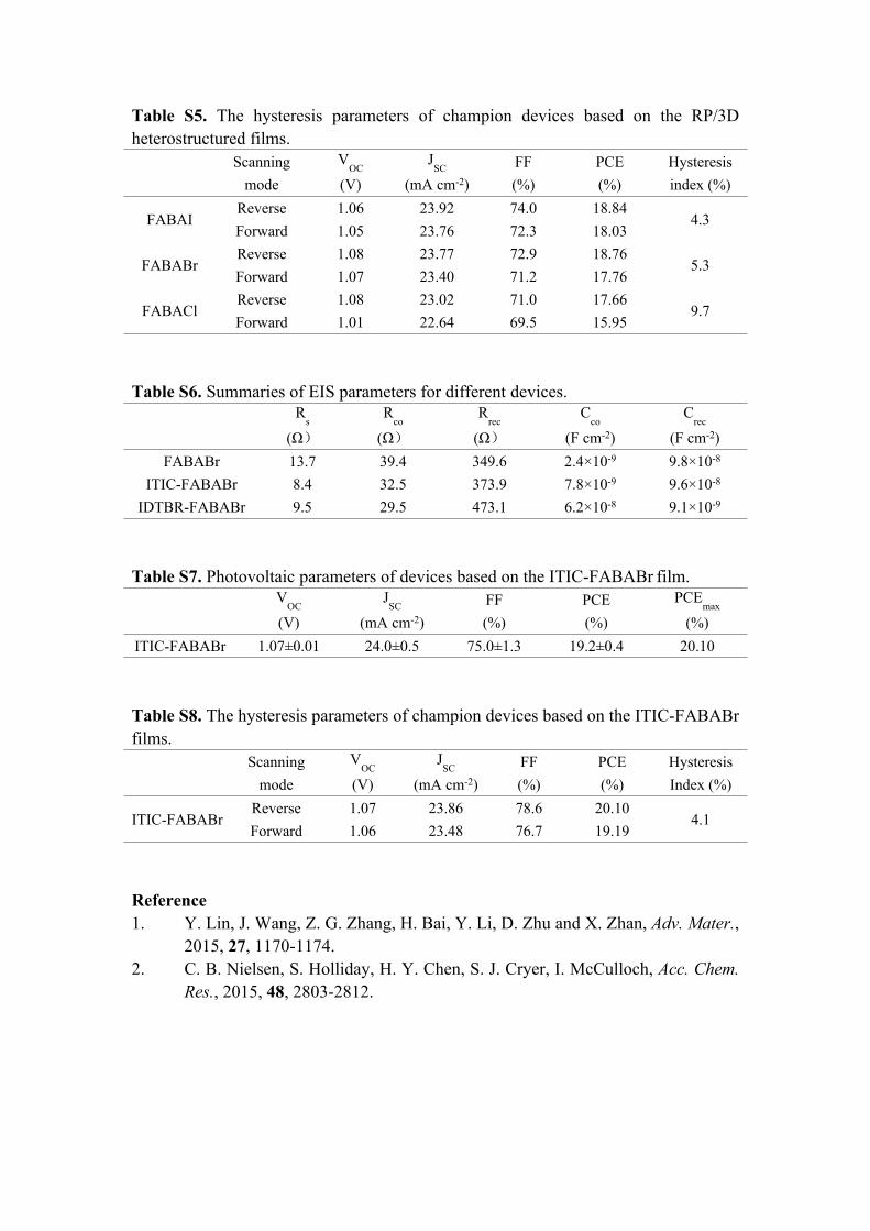
Table S5. The hysteresis parameters of champion devices based on the RP/3D heterostructured films.
Scanningmode
VOC
(V)
JSC
(mA cm-2)FF(%)
PCE(%)
Hysteresisindex (%)
Reverse 1.06 23.92 74.0 18.84FABAI
Forward 1.05 23.76 72.3 18.034.3
Reverse 1.08 23.77 72.9 18.76FABABr
Forward 1.07 23.40 71.2 17.765.3
Reverse 1.08 23.02 71.0 17.66FABACl
Forward 1.01 22.64 69.5 15.959.7
Table S6. Summaries of EIS parameters for different devices.R
s
(Ω)
Rco
(Ω)
Rrec
(Ω)
Cco
(F cm-2)
Crec
(F cm-2)FABABr 13.7 39.4 349.6 2.4×10⁻⁹ 9.8×10⁻⁸
ITIC-FABABr 8.4 32.5 373.9 7.8×10⁻⁹ 9.6×10⁻⁸
IDTBR-FABABr 9.5 29.5 473.1 6.2×10⁻⁸ 9.1×10⁻⁹
Table S7. Photovoltaic parameters of devices based on the ITIC-FABABr film.V
OC
(V)
JSC
(mA cm-2)FF(%)
PCE(%)
PCEmax
(%)ITIC-FABABr 1.07±0.01 24.0±0.5 75.0±1.3 19.2±0.4 20.10
Table S8. The hysteresis parameters of champion devices based on the ITIC-FABABr films.
Scanningmode
VOC
(V)
JSC
(mA cm-2)FF(%)
PCE(%)
HysteresisIndex (%)
Reverse 1.07 23.86 78.6 20.10ITIC-FABABr
Forward 1.06 23.48 76.7 19.194.1
Reference1. Y. Lin, J. Wang, Z. G. Zhang, H. Bai, Y. Li, D. Zhu and X. Zhan, Adv. Mater.,
2015, 27, 1170-1174.2. C. B. Nielsen, S. Holliday, H. Y. Chen, S. J. Cryer, I. McCulloch, Acc. Chem.
Res., 2015, 48, 2803-2812.