swansea 2016 ts fin - actinpak - active and intelligent fibre-based … · 2017-07-18 ·...
TRANSCRIPT

Interduction of R&D activities
Challenges and aspects of printed/coated functionalities
Materials
Selected devices/functionalities
Coating techniques
Printing techniques
Drying/Sintering techniques
Conclusion
Interduction of R&D activities
Challenges and aspects of printed/coated functionalities
Materials
Selected devices/functionalities
Coating techniques
Printing techniques
Drying/Sintering techniques
Conclusion
Agenda
Department of Graphic Arts and Photophysics
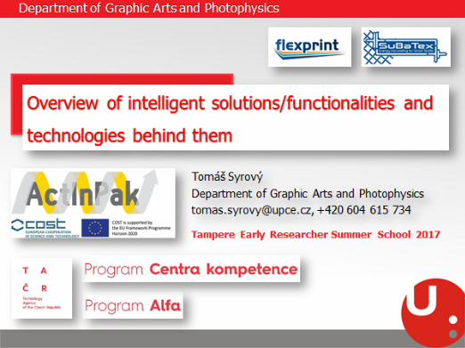
Syrovy
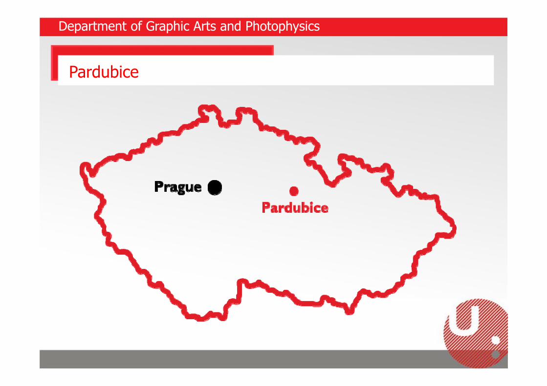
Pardubice
Department of Graphic Arts and Photophysics
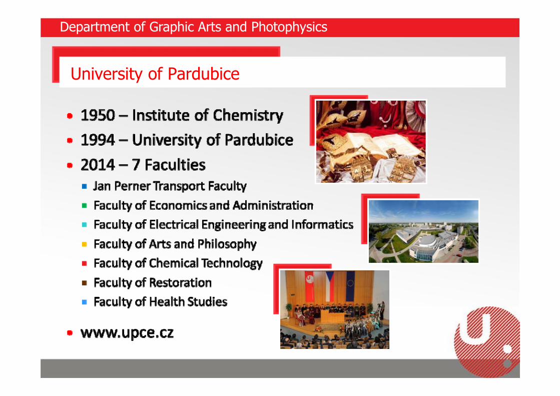
University of Pardubice
Department of Graphic Arts and Photophysics
Department of graphic arts and photophysics
Department of Graphic Arts and Photophysics
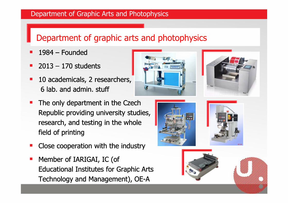
1984 – Founded
2013 – 170 students
10 academicals, 2 researchers, 6 lab. and admin. stuff
The only department in the Czech Republic providing university studies, research, and testing in the whole field of printing
Close cooperation with the industry
Member of IARIGAI, IC (of Educational Institutes for Graphic Arts Technology and Management), OE-A

R&D activities
Department of Graphic Arts and Photophysics
Simple functional layers Antistatic, Antimicrobial, Security
Luminescent, Photochromic
Passive components Resistors Capacitors, Coils Etc.
OECT, OFET Printed batteries
Alkaline, Li-on
Simple functional layers Antistatic, Antimicrobial, Security
Luminescent, Photochromic
Passive components Resistors Capacitors, Coils Etc.
OECT, OFET Printed batteries
Alkaline, Li-on
Sensors Temperature s. Rel. humidity s. Gas s. Air/Gas flow s. Acceleration s. Tactile s. Light s.
Display elements LEC, OLED Electrochromic
Smart Labels With NFC
communicationover Android devices
Sensors Temperature s. Rel. humidity s. Gas s. Air/Gas flow s. Acceleration s. Tactile s. Light s.
Display elements LEC, OLED Electrochromic
Smart Labels With NFC
communicationover Android devices Core Projects - TE01020022 www.flexprint.cz
TA04010085 - Flexible autonomous energy harvesting systems for smart textiles Core Projects - TE01020022 www.flexprint.cz
TA04010085 - Flexible autonomous energy harvesting systems for smart textiles
Contact: [email protected], +420 604 615 734
Experiences R&D of Inks & printing/coating technology process Upscaling, Lab2Fab experineces incl. Wide Web
Experiences R&D of Inks & printing/coating technology process Upscaling, Lab2Fab experineces incl. Wide Web

R&D activities, printing/coating techniques competency
Department of Graphic Arts and Photophysics
R&D of technology of preparation of functional structures R&D of ink formulation and benchmarking of comercial ink formulation Personally 400-800 mixed/tested ink formulations per year for several type
of printing/coating techniques and applications
R&D of technology of preparation of functional structures R&D of ink formulation and benchmarking of comercial ink formulation Personally 400-800 mixed/tested ink formulations per year for several type
of printing/coating techniques and applications
Screen printing(Sheet fed, R2R)
Flexo Gravure Pad printing Offset IJ
Spin coating Dip coating Spiral bar coating Spray coating Zone casting AJP
Screen printing(Sheet fed, R2R)
Flexo Gravure Pad printing Offset IJ
Spin coating Dip coating Spiral bar coating Spray coating Zone casting AJP
Lab2Fab experiences Narrow web (410 mm), Wideweb production trials, pilot plant trials incl.
high speed materiál printing (1.3 m, 320 m/min)
Negative patterning – lasers – UV/VIS, NIR, IR

The printing and coating techniques should provide cheap and fast production of low costand low-end functionalities
Printed/coated functionalities are sometimes tens years behind to products made by traditional technologies in terms of their characteristics
The printing and coating techniques should provide cheap and fast production of low costand low-end functionalities
Printed/coated functionalities are sometimes tens years behind to products made by traditional technologies in terms of their characteristics
Why coating and printing technologies?
Department of Graphic Arts and Photophysics
SOMA

Safety - printing materials, fabrication process
Printing/coating materials, printing substrates
Printing forms
Interaction of materials
Strict observance of technology
Printing/coating process quality/stability
Post treatment condition
Storing of the products
Long term stability
Never-ending and limitless opportunities to use or characterize anything
Differences to conventional coating/printing process?
Department of Graphic Arts and Photophysics
(NASA)
Syrovy

Printed/coated functionalities
Department of Graphic Arts and Photophysics
Active components/structures Battery (primary, secondary) Battery Charger Photovoltaic – PV – (OPV, DSSC) Display, Light source – OLED, EL,
electrochromic, thermochromic, electroforetic
Sensor – chemical, bio, climatic, pressure, etc.
Memory RFID diodes Transistors – OFET, OECT ISS – Smart Objects, Smart Sensor,
Smart Textiles
Functional layers• Healtcare aplication• Drugs• Termochromic, photochromic• Catalytic layer• Textile finishing layers• Explosives
Functional layers• Healtcare aplication• Drugs• Termochromic, photochromic• Catalytic layer• Textile finishing layers• Explosives
Passive components• Electronic circuits • Antennas – RFID• Capacitors, resistors, induction coil,
transformers
Passive components• Electronic circuits • Antennas – RFID• Capacitors, resistors, induction coil,
transformers

Simple functional layers
Department of Graphic Arts and Photophysics
Antistatic Antimicrobial Barrier UV protective Luminescent Thermochromic Photochromic Electromagnetic shielding
Antistatic Antimicrobial Barrier UV protective Luminescent Thermochromic Photochromic Electromagnetic shielding
Syrovy

Luminiscent materials
Department of Graphic Arts and Photophysics
R&D of specific effect layers Fluorescencent
R&D of specific effect layers Fluorescencent
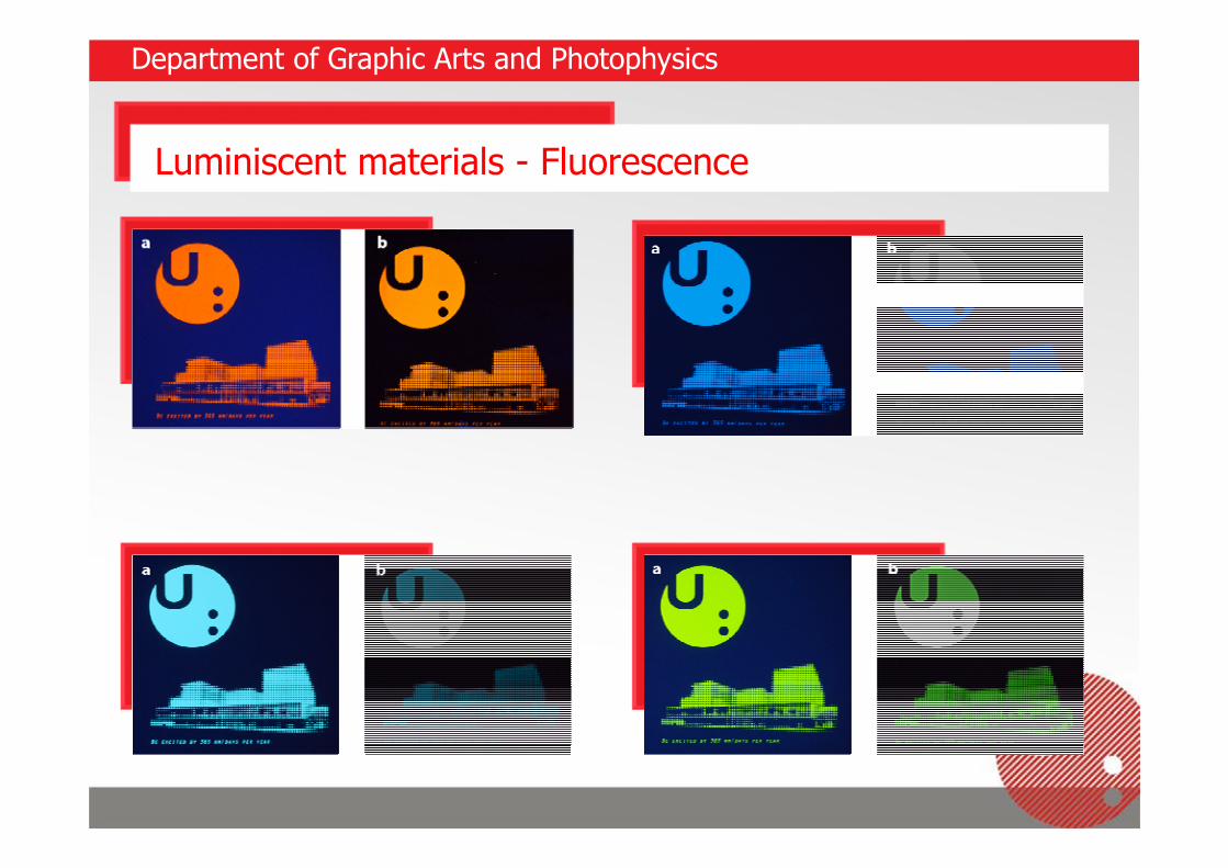
Luminiscent materials - Fluorescence
Department of Graphic Arts and Photophysics

Substrates for printed functionalities/electronics
Department of Graphic Arts and Photophysics
Flexible PET, PEN, PI (Kapton, Neopulim), PC, PVC Polyolefins - PE, PP Synthetic papers – Pretex (PES/PA), Synaps (PES), Tyvek
(HDPE), Teslin (polyolefin) Paper – un/coated paper, primer Nanocellulose Glass – 25 to 100 μm Metals
Rigid Paper - heavy ream weight Cardboard Thick polymeric susbtrate (PET, PEN, PI, PC, PE, PP, etc.) Glass – float, quartz, etc. Ceramic – Al2O3 (Rubalit, Alunit), AlN, etc. Metals
Polyimide
PET
Ultra-Thin Glass - SCHOTT
CeramTec

Materials for printed/coated structures
Department of Graphic Arts and Photophysics
Yang www.lehigh.edu

Materials for printed/coated structures
Department of Graphic Arts and Photophysics
Conductive Metal composite – based on (Ag, Cu, Au, Ni, Pt,
etc.) Different shape and sizes of particles
(globular, flakes, rods, wires) Ag based most used
Up to 30 % of conductivity of bulk Ag Cu – usually based on precursors CuO
Photonic sintering, reduction agents Other metal for specific purposes
High temperature firing – Ag, Au, Pt, etc. Precursors of metals
Carbon composite (graphite, carbon black, etc.)
Carbon based (graphene, GNPCNT (SWCNT, MWCNT))
Zhu et All.
Syrovy mntl.illinois.edu
Syrovy

Materials for printed/coated structures - (Semi)conductive
Department of Graphic Arts and Photophysics
Polymers PEDOT:PSS – (in-situ 3000 S/cm, disp. 1000 S/cm) Polyaniline Polyacetylene Polypyrrole Polythiofene MEH-PPV PVK, etc.
Small molecules TIPS - Pentacene Rubrene Phtalocyanines Diketopyrrolopyrrole Perylenes Alq3, NPD, TPD, Ru cpx Some others Fullerenes
Polymers PEDOT:PSS – (in-situ 3000 S/cm, disp. 1000 S/cm) Polyaniline Polyacetylene Polypyrrole Polythiofene MEH-PPV PVK, etc.
Small molecules TIPS - Pentacene Rubrene Phtalocyanines Diketopyrrolopyrrole Perylenes Alq3, NPD, TPD, Ru cpx Some others Fullerenes
polypyrrole
PEDOT:PSS
2014, Xue et Al.
Materials for printed/coated structures - semiconductive
Department of Graphic Arts and Photophysics
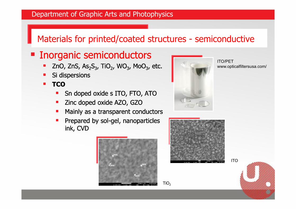
Inorganic semiconductors ZnO, ZnS, As2S3, TiO2, WO3, MoO3, etc. Si dispersions TCO Sn doped oxide s ITO, FTO, ATO Zinc doped oxide AZO, GZO Mainly as a transparent conductors Prepared by sol-gel, nanoparticles
ink, CVD
Inorganic semiconductors ZnO, ZnS, As2S3, TiO2, WO3, MoO3, etc. Si dispersions TCO Sn doped oxide s ITO, FTO, ATO Zinc doped oxide AZO, GZO Mainly as a transparent conductors Prepared by sol-gel, nanoparticles
ink, CVD
ITO/PET www.opticalfiltersusa.com/
ITO
TiO2

Materials for printed/coated structures - dielectrics
Department of Graphic Arts and Photophysics
Polymer based From solution/dispersion of various polymers
PVC (ε’ ~ 3) PC (ε’ ~ 2.8 – 3.4) PVDF (ε’ ~ 6) PMMA (ε’ ~ 3)
Radiation induced polymerization (UV, EB)(Acrylate based (ε’ ~ 3))
Thermally induced polymerization (PVP, acrylates with proper iniciators)
Composites Based on particles of inorganic materials with high dielectric
constant BaTiO3 (ε’ ~ 1000) SrTiO3 (ε’ ~ 300) TiO2 (ε’ ~ 100) Al2O3, MgO (ε’ ~ 9) HfO2 (ε’ ~ 20)
Poly(4-vinylphenol)
Kharisov et Al.

Passive electronic components
Department of Graphic Arts and Photophysics
ResistorsCapacitorsCircuits and conductivestructuresTransparent conductive electrode (Semi)conductive polymers CNT, graphene based layers Metals nanowires layers high-resolution conductive metal (metal
mesh)
ResistorsCapacitorsCircuits and conductivestructuresTransparent conductive electrode (Semi)conductive polymers CNT, graphene based layers Metals nanowires layers high-resolution conductive metal (metal
mesh)
PolyIC
Syrovy
Syrovy

RFID
Department of Graphic Arts and Photophysics
RFID (Radio Frequency Identification) – system which through the radio-frequency electromagnetic fields transfer data, usually for the automatic identification and tracking tags attached to objects.
The datas are stored inside tag. These datas is possible to read or rewrite in dependance to type od tag.
Every TAG has an unique EPC.
Implementation of RFID requires except tag, readers and „middleware“ (Central systém for data exchange, storing, it is gate to MIS)
(Hrachovcová)
Syrovy

RFID – type of TAGs
Department of Graphic Arts and Photophysics
Active TAG Battery is a main source of the energy, which limit lifecycle.
This type of TAG is usually equiped by MCU, sensors, I/O ports.
It is used for more advance type of aplication – ISS. Usually has a higher price due to more complicated production than for passive tags.
Tag start the communication as a first, followed by response of reader, peridodically transmits its ID signal.
The active tags are used for identification, localization of fast moving object too.
The read distance is in range of hundreds meters.
Semi-active TAG For transfer of datas use energy emmited by readers. Communication is activated by reades, the battery source is used
for data transfer to higher distances.
The read distance is in range of tens of meters (UHF, MW).
Identification, localization of fast moving object.
Longer lifecycle than for active tag.

RFID – type of TAGs
Department of Graphic Arts and Photophysics
Passive TAG The communication starts reader. Energy for communication is obtained from electromagnetic filed generated by reader. Low cost, more simple structure, durability and resistance to extreme condition (temperature to 200 °C, acids,
bases) The passive tag consist from antenna and chip. At higher frequencies there are difficulties with interferences
and identification close to metals and liquids. The passive tags are cheaper and smaller in comparison to active tags. Usability –logistics (material flow), personal ID cards, passports, credit cards, identification of vehicles, animals,
books in libbraries
2012, Schmoldt

RFID – Frequencies
Department of Graphic Arts and Photophysics
Read distance – Induction (Near Field Comunication), reflection (Far Field) Memory - Tag RO (Read-Only), Tag WORM (Write Once Read Many), Tag
RW (Read-Write) Class – according abilities, Class 0 - 5
Read distance – Induction (Near Field Comunication), reflection (Far Field) Memory - Tag RO (Read-Only), Tag WORM (Write Once Read Many), Tag
RW (Read-Write) Class – according abilities, Class 0 - 5
2012, Schmoldt

RFID - Frequencies
Department of Graphic Arts and Photophysics
(Hrachovcová)
Low Frequency125 a 135 KHz
LF Tag
- Read distance up to 0,5 m, low communication speed- High cost of production- no difficult to read when placed within a few millimetres of a metal or
liquid surface- ID card, animals identification
High Frequency13,56 MHz
HF Tag
- Read distance up to 1 m, moderate communication speed- High cost of production- Difficulties with reading through the liquid- logistics, identification of goods
Ultra High Frequency868 MHzUHF Tag
- Read distance up to 3 m, high communication speed- Low cost production- Difficulties with reading through the liquid and metals
Microwave2,45 a 5,8 GHz
MW Tag
- Read distance up to 10 m
- identification of fast moving objects- High cost of tag

RFID – Production
Department of Graphic Arts and Photophysics
Etching Cu, Al (18 – 35 µm) Galvanic metallization of vacum
evaporated/sputtered structures Laser ablation – negative
patterning Printing technique Silver, copper (precursor)
based inks Screen printing – the most
used Gravure Flexography
Etching Cu, Al (18 – 35 µm) Galvanic metallization of vacum
evaporated/sputtered structures Laser ablation – negative
patterning Printing technique Silver, copper (precursor)
based inks Screen printing – the most
used Gravure Flexography
Impe
danc
e[ k
]
0
5
10
15
20
25
106 107 108 109
Frequency [Hz]
Impe
danc
e[ k
]
0
5
10
15
20
25
106 107 108 109
Frequency [Hz]
OTK Group

Printed batteries
Department of Graphic Arts and Photophysics
Based on typical materials and chemistry as for conventional batteries
Flexible, Thin - usually below 1 mm R2R compatible production process Capacity in range of tens of mAh Voltage in dependence to electrode
materials and electrolytes Basic patrameters – Nominal Voltage,
Capacity, short-circuit current, UI characteristics
For device with low consumption of electrical energy < 1 mW
Usage – ISS, RFID, sensors, chip cards, etc.
Syrovy
Printed baterries, accumulators - materials
Department of Graphic Arts and Photophysics
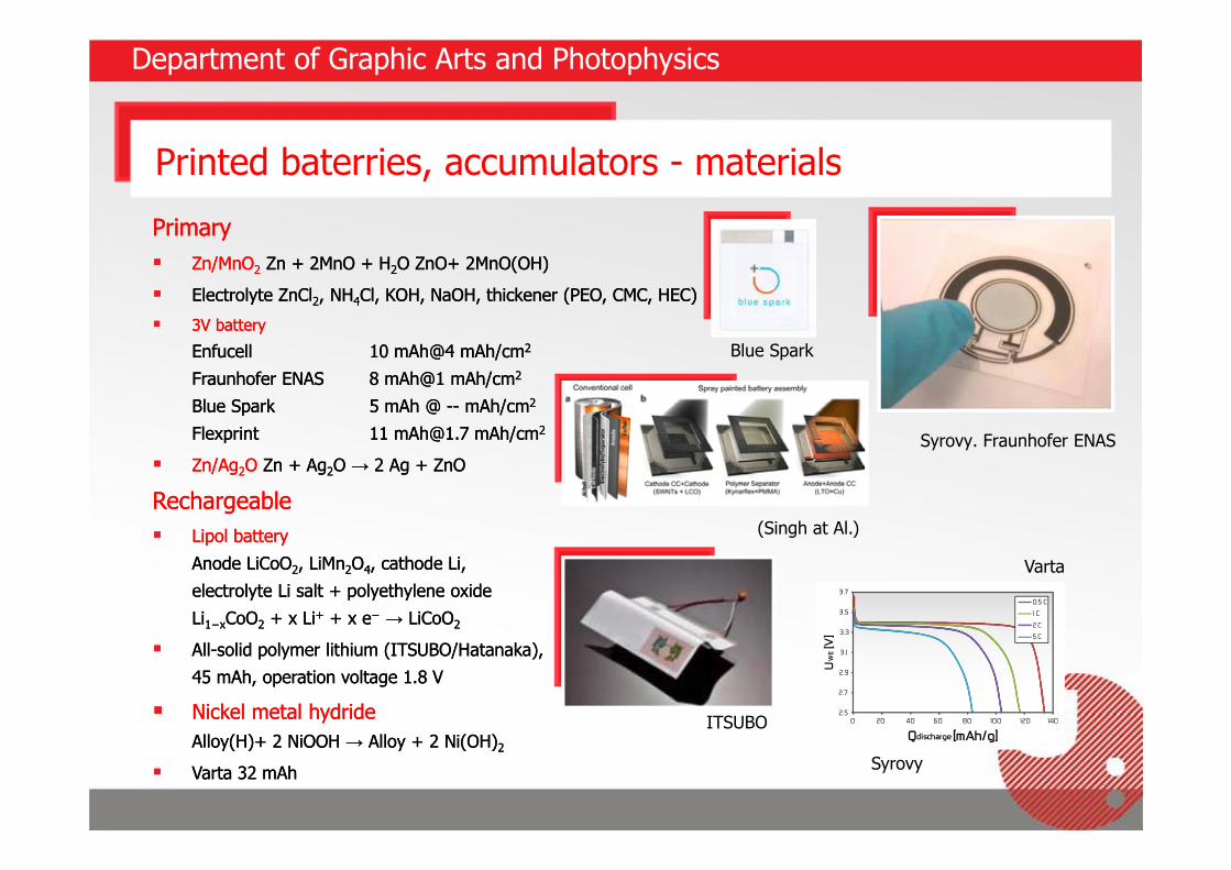
Primary Zn/MnO2 Zn + 2MnO + H2O ZnO+ 2MnO(OH) Electrolyte ZnCl2, NH4Cl, KOH, NaOH, thickener (PEO, CMC, HEC) 3V battery
Enfucell 10 mAh@4 mAh/cm2
Fraunhofer ENAS 8 mAh@1 mAh/cm2
Blue Spark 5 mAh @ -- mAh/cm2
Flexprint 11 [email protected] mAh/cm2
Zn/Ag2O Zn + Ag2O → 2 Ag + ZnO
Rechargeable Lipol battery
Anode LiCoO2, LiMn2O4, cathode Li,electrolyte Li salt + polyethylene oxideLi1−xCoO2 + x Li+ + x e− → LiCoO2
All-solid polymer lithium (ITSUBO/Hatanaka), 45 mAh, operation voltage 1.8 V
Nickel metal hydride Alloy(H)+ 2 NiOOH → Alloy + 2 Ni(OH)2
Varta 32 mAh
ITSUBO
Varta
Syrovy. Fraunhofer ENAS
Blue Spark
(Singh at Al.)
Qdischarge [mAh/g]
UW
E[V
]
2.5
2.7
2.9
3.1
3.3
3.5
3.7
0 20 40 60 80 100 120 140
0.5 C
1 C
2 C
5 C
Qdischarge [mAh/g]
UW
E[V
]
2.5
2.7
2.9
3.1
3.3
3.5
3.7
0 20 40 60 80 100 120 140
0.5 C
1 C
2 C
5 C
Syrovy

Supercapacitors, Hybrid capacitors
Department of Graphic Arts and Photophysics
Charge/discharge current is in range 1-100 A.
Very low value of internal resistance 10 times higher energy density in comparison
to clasic capacitors. Charging time is in orders shorter to batteries. Capacity is directly proportional to the area and
inversely proportional to the distance between the electrodes
Capacity is given by electrodes materials too. Usability – ISS, RFID, sensors,
chipcards, etc. Basic patrameters – Nominal Voltage, Capacity,
short-circuit current, UI characteristics
Parameter Batteries Capacitors Supercapacitors
Energy density[Wh/kg] 100 0,2 10
Specific power[kW/kg] 1-3 500 10
Charging time 5 h 0,001 s 10 s
Life cycle 100 1 000 000 1 000 000
Dvorak

Storage principles
Department of Graphic Arts and Photophysics
Pseudocapacitance storage
of the electrical energy basedon reversible redox reactionswith charge-transfer.
EDLC (Electric Double Layer
Capacitor) Based on separation of charge in a Helmholtz double layer.
Pseudocapacitance storage
of the electrical energy basedon reversible redox reactionswith charge-transfer.
EDLC (Electric Double Layer
Capacitor) Based on separation of charge in a Helmholtz double layer.
Dvořák
ScienceDirect
Syrovy

Electrode materials, electrolytes
Department of Graphic Arts and Photophysics
Electrode materials Carbon based materials with large
specific surface (> 1000 m2/g) (Semi)conductive polymers Metal oxides
Electrolytes Water based solution of acids
(H2SO4. H3PO4), bases (KOH) and salts (NaClO4, LiClO4, LiAsF6)
High specific conductivity (100-1000 mS/cm), Low operation window ~ 1 V per electrode, low operation temperature.
Organic solvents – the most often solvents are propylene carbonate, ethylene carbonate, tetrahydrofuran, diethyl carbonate, γ-butyrolactone. Salts - LiClO4, Et4NPF6, Bu4NPF6.
An advantage of organic solvents is higher operation voltage (up to 4 V). The electrical conductivity of electrolytes based on organic solvents is lower (10 to 60 mS/cm). Energy density increases with the square of the voltage.
Dvořák

Photovoltaic cells
Department of Graphic Arts and Photophysics
DSSC „Grätzel cell“ – 1991 High efficiency up to 12 % 2014 DSSC with
perovskite up to 20.5 %
OPV Commercial avaiable from 2009
with Wp 1 – 28 W Efficiency at 12 % is comparable
with 15 % for conventional Si panels
Integration of OPV from 2010
DSSC „Grätzel cell“ – 1991 High efficiency up to 12 % 2014 DSSC with
perovskite up to 20.5 %
OPV Commercial avaiable from 2009
with Wp 1 – 28 W Efficiency at 12 % is comparable
with 15 % for conventional Si panels
Integration of OPV from 2010
Solarprint)
NREL
Heliatek

DSSC - materials
Department of Graphic Arts and Photophysics
Photoelectrode TiO2, ZnO, Fe2O3, ZrO2, Nb2O5, Al2O3, CeO2, SrTiO3, Zn2SnO4
Shapes of particles - globular, microsheets, nanorods, nanotubes, nanorods
Sensibilizing dyes Bipyridyl ruthenium complex
Counter electrode Platinum (H2PtCl6)
Carbon based (graphite, CNT)
(Semi)conductive polymers
Electrolytes Liquid, gel, solid state
redox systems I/I3-, Br−/Br3
−, SCN−/SCN2−, SeCN−/SeCN2
−, 1-hexyl-3-methylimidazolium iodide
Acetonitrile, propionitrile, methoxyacetonitrile, NMP, EG, etc.
polyethylene glycol (PEG), 1,3:2,4-di-O-dimethylbenzylidene-D-sorbitol (DBS), poly(acrylicacid)-poly(ethylene glycol) (PEG-PAA), polyvinylpyridine (PVP), polyacrylonitrile (PAN)
Syrový et Al.

Photoelectrode
Department of Graphic Arts and Photophysics
Xu et al., 2010; Wang et al., 2010; Gao et al., 2007; Pang et al., 2007

Sensibilizing dyes
Department of Graphic Arts and Photophysics
Le Bahers et Al.
Hatala, Syrovy

DSSC with perovskite
Department of Graphic Arts and Photophysics
In 2009 3.8% efficiency Based on TiO2, Al2O3 photoelectrode Perovskite acting not only as a light
absorber, but as a charge-carrying semiconductor
Organometal halides CH3NH3PbI3 withperovskite structure
efficiency approaching 20% isrealistically possible from a solid-state mesoscopic solar cell based on CH3NH3PbX3
In tandem cells with silicon based panel efficiencies should be expected 30% or more
Extremely sensitive to oxygen, water vapor dissolves the salt like perovskites
Solarprint)
Park

OPV
Department of Graphic Arts and Photophysics
Based on p-conjugated smallmolecules or polymers
Typical energy gaps of 1 to 3 eV between LUMO and HOMO
Power conversion efficiency (PCE, ηP) has steadily increased over the years from about 6% to 14%
Based on p-conjugated smallmolecules or polymers
Typical energy gaps of 1 to 3 eV between LUMO and HOMO
Power conversion efficiency (PCE, ηP) has steadily increased over the years from about 6% to 14%
2014, Xue et Al 2014, Bessette
2014, Andersen

OPV - materials
Department of Graphic Arts and Photophysics
2014, Xue et Al.Vanmaele
OPV R2R fabrication
Department of Graphic Arts and Photophysics
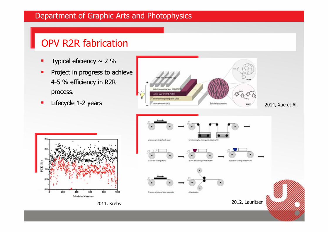
Typical eficiency ~ 2 % Project in progress to achieve
4-5 % efficiency in R2R process.
Lifecycle 1-2 years
Typical eficiency ~ 2 % Project in progress to achieve
4-5 % efficiency in R2R process.
Lifecycle 1-2 years 2014, Xue et Al.
2011, Krebs 2012, Lauritzen

OLED
Department of Graphic Arts and Photophysics
Several types called PMOLED, AMOLED, PHOLED, WOLED, FOLED, TOLED, SOLED
High efficiency 50.7 lm/W at 1000 cd/m2, 140 lm/W for SOLED
Up to 200 000 cd/m2
Several types called PMOLED, AMOLED, PHOLED, WOLED, FOLED, TOLED, SOLED
High efficiency 50.7 lm/W at 1000 cd/m2, 140 lm/W for SOLED
Up to 200 000 cd/m2
Guaino
SyrovyNovaled
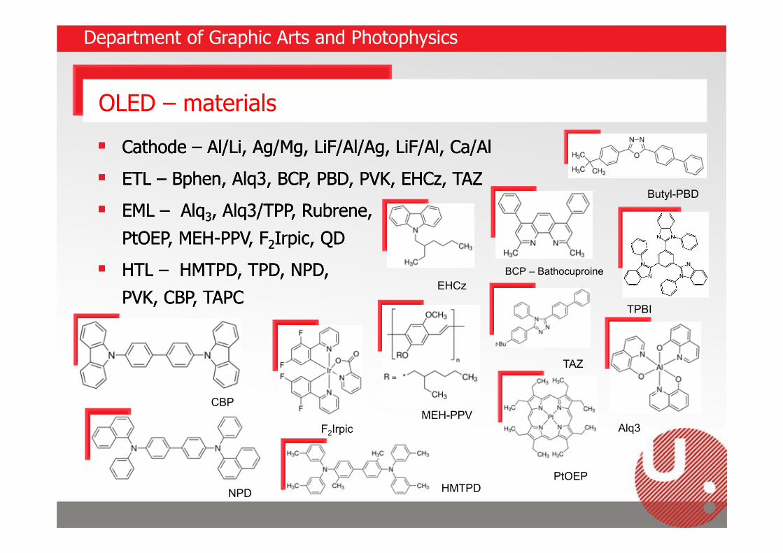
OLED – materials
Department of Graphic Arts and Photophysics
Cathode – Al/Li, Ag/Mg, LiF/Al/Ag, LiF/Al, Ca/Al ETL – Bphen, Alq3, BCP, PBD, PVK, EHCz, TAZ EML – Alq3, Alq3/TPP, Rubrene,
PtOEP, MEH-PPV, F2Irpic, QD HTL – HMTPD, TPD, NPD,
PVK, CBP, TAPC
Cathode – Al/Li, Ag/Mg, LiF/Al/Ag, LiF/Al, Ca/Al ETL – Bphen, Alq3, BCP, PBD, PVK, EHCz, TAZ EML – Alq3, Alq3/TPP, Rubrene,
PtOEP, MEH-PPV, F2Irpic, QD HTL – HMTPD, TPD, NPD,
PVK, CBP, TAPCBCP – Bathocuproine
EHCz
TAZ
MEH-PPV
PtOEP
Alq3
TPBI
Butyl-PBD
CBP
HMTPD
F2Irpic
NPD

OLED
Department of Graphic Arts and Photophysics
HowStufWorks

Light emmiting capacitors - LEC
Department of Graphic Arts and Photophysics
Based on doped luminofors of ZnS, SrS, etc.
High efficiency up to 37 %, rsp. 160 lm/W, low consumption 34 W/m2
Life cycle > 12 500 hour Backlight for advertising
displays, decorative lighting, security lighting, backlighting dashboards.
Based on doped luminofors of ZnS, SrS, etc.
High efficiency up to 37 %, rsp. 160 lm/W, low consumption 34 W/m2
Life cycle > 12 500 hour Backlight for advertising
displays, decorative lighting, security lighting, backlighting dashboards.
Solarmer)
Syrovy
SyrovySyrovy
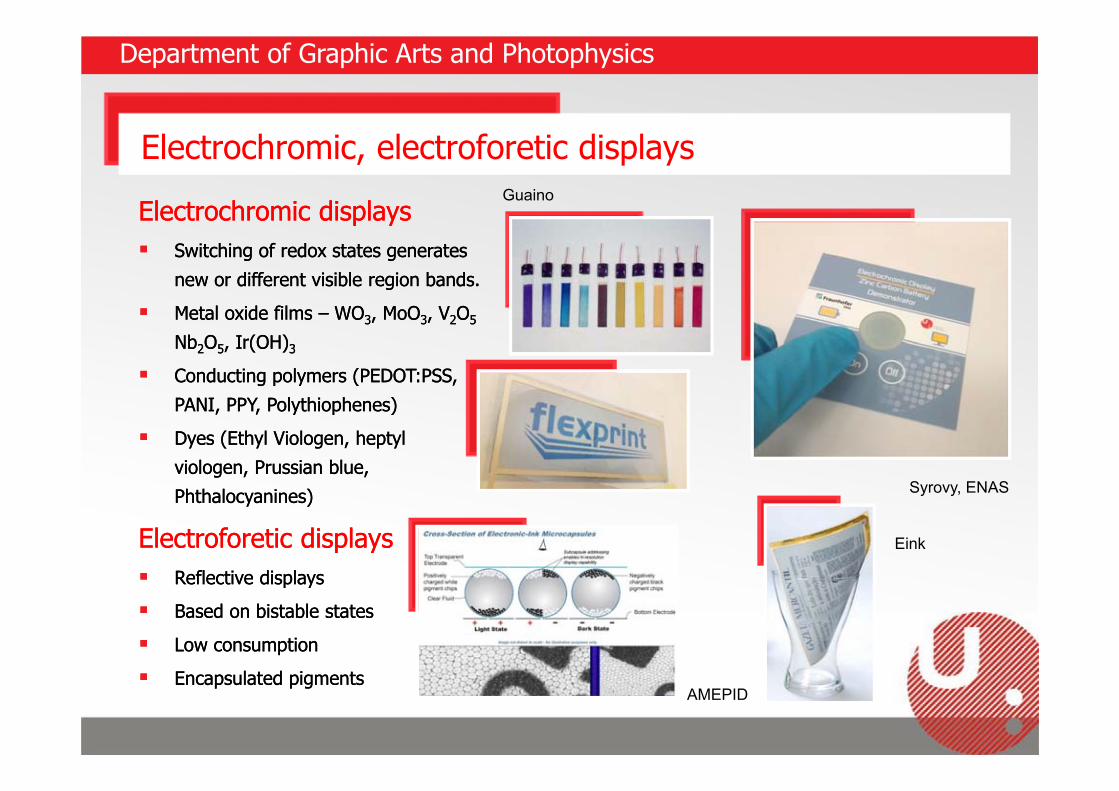
Electrochromic, electroforetic displays
Department of Graphic Arts and Photophysics
Electrochromic displays Switching of redox states generates
new or different visible region bands. Metal oxide films – WO3, MoO3, V2O5
Nb2O5, Ir(OH)3
Conducting polymers (PEDOT:PSS, PANI, PPY, Polythiophenes)
Dyes (Ethyl Viologen, heptyl viologen, Prussian blue, Phthalocyanines)
Electroforetic displays Reflective displays Based on bistable states Low consumption Encapsulated pigments
Guaino
AMEPID
Syrovy, ENAS
Eink
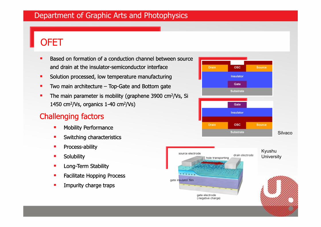
OFET
Department of Graphic Arts and Photophysics
Based on formation of a conduction channel between source and drain at the insulator-semiconductor interface
Solution processed, low temperature manufacturing Two main architecture – Top-Gate and Bottom gate The main parameter is mobility (graphene 3900 cm2/Vs, Si
1450 cm2/Vs, organics 1-40 cm2/Vs)
Challenging factors Mobility Performance Switching characteristics Process-ability Solubility Long-Term Stability Facilitate Hopping Process Impurity charge traps
Silvaco
KyushuUniversity

OFET – materials
Department of Graphic Arts and Photophysics
n type – PTCDA, PCBM, DBP, BBL p type – P3HT, PQT, PTAA,
TIPS pentacene, CuPc, Caronene,Rubrene
Dielectric – PMMA, PS, etc.
n type – PTCDA, PCBM, DBP, BBL p type – P3HT, PQT, PTAA,
TIPS pentacene, CuPc, Caronene,Rubrene
Dielectric – PMMA, PS, etc.
PCBM
DBPBBL
TPBI
PTCDA
P3HT
CuPc TIPS P.
PTAA

OECT
Department of Graphic Arts and Photophysics
Switching of redox states of channel affectsIds, resistivity of channel respectively.
Two main architecture – Latteral, sandwich Low voltage operation, On/OFF up to 105
Response time in ms
Switching of redox states of channel affectsIds, resistivity of channel respectively.
Two main architecture – Latteral, sandwich Low voltage operation, On/OFF up to 105
Response time in ms
Syrovy
S DG
S DG

Sensors
Department of Graphic Arts and Photophysics
Temperature Relative humidity Gas detection – NO2, SO2,
H2, NH3, H2S, Ethylene, hydrocarbons Movement sensors, acceleration sensors Tactile sensors, pressure sensors Light sensors Biosensors Electrochemic Microfluidic
Temperature Relative humidity Gas detection – NO2, SO2,
H2, NH3, H2S, Ethylene, hydrocarbons Movement sensors, acceleration sensors Tactile sensors, pressure sensors Light sensors Biosensors Electrochemic Microfluidic
Syrovy

Others printed functionalities
Department of Graphic Arts and Photophysics
Printed memory ROM, WORM, NVRAM
Printed speakers Electromagnetic induction Piezoelectric
Electro active polymers Artificial muscles Tactile sensors Haptic feedback Tactile displays „artificial skin“ Energy generator
Printed memory ROM, WORM, NVRAM
Printed speakers Electromagnetic induction Piezoelectric
Electro active polymers Artificial muscles Tactile sensors Haptic feedback Tactile displays „artificial skin“ Energy generator
2013, Jung
Rowland
Hübler
OE-A
Heydt Bosh

Spin coating
DIP coating
Doctor blade, Bar Coating
Spray coating
Ink-Jet
Aerosol printing
Electro-Hydrodynamic and Reciprocating System
Spin coating
DIP coating
Doctor blade, Bar Coating
Spray coating
Ink-Jet
Aerosol printing
Electro-Hydrodynamic and Reciprocating System
Coating and printing techniques – laboratory
Department of Graphic Arts and Photophysics
Pasquarelli et Al.
Optomec

Spin Coating. Spray Coating, Blade Coating, Spiral Bar Coating DSSC – TiO2 photoelectrode, counter electrode
OPV – HIL layer, ETL, BHJ layer
Transparent conductive layers
Metal bus bars, wiring
Spin Coating. Spray Coating, Blade Coating, Spiral Bar Coating DSSC – TiO2 photoelectrode, counter electrode
OPV – HIL layer, ETL, BHJ layer
Transparent conductive layers
Metal bus bars, wiring
Laboratory scale Printing/Coating techniques in photovoltaics
Department of Graphic Arts and Photophysics
Kang et al.
[1] Yu et. al., IEEE Journal of Selected Topics in Quantum Electronics 2010 10.1109/JSTQE.2010.2042282[2] Steirer et. al., Solar Energy Materials and Solar Cells 2009 10.1016/j.solmat.2008.10.026[3] Zhao et. al., Journal of Bionanoscience 2012 10.1166/rnn.2012.1011[4] Girotto et. al., Solar Energy Materials and Solar Cells 2009 10.1016/j.solmat.2008.11.052[5] Girotto et. al., Advanced Functional Materials 2011 10.1002/adfm.201001562[6] Kang et. al., Solar Energy Materials and Solar Cells 2012 10.1016/j.solmat.2012.04.027[7] Lewis et. al., Solar Energy Materials and Solar Cells 2011 10.1016/j.solmat.2011.05.037[8] Colella et. al., Applied Physics Letters 2013 10.1063/1.4807464[9] Emslie et. al., Journal of Applied Physics 1958 10.1063/1.1723300[10] Meyerhofer et. al., Journal of Applied Physics 1978 10.1063/1.325357[11] Lange et. al., Solar Energy Materials and Solar Cells 2013 10.1016/j.solmat.2012.10.011[12] Eom et. al., Organic Electronics 2009 10.1016/j.orgel.2009.01.015[13] Galagan et. al., Solar Energy Materials and Solar Cells 2012 10.1016/j.solmat.2012.04.039[14] Huang et. al., Organic Electronics 2013 10.1016/j.orgel.2013.08.001[15] Yu et. al., Nanoscale 2012 10.1039/c2nr31508d
PEMS
Yulia Galagan et al.
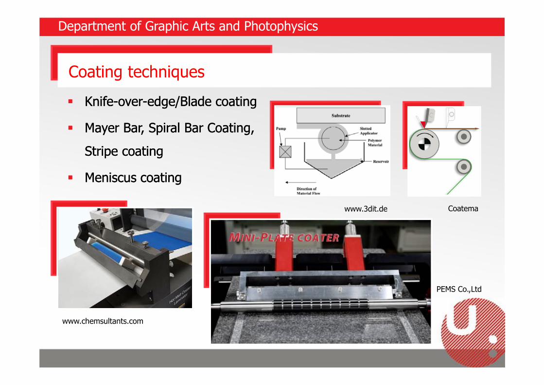
Knife-over-edge/Blade coating
Mayer Bar, Spiral Bar Coating, Stripe coating
Meniscus coating
Knife-over-edge/Blade coating
Mayer Bar, Spiral Bar Coating, Stripe coating
Meniscus coating
Coating techniques
Department of Graphic Arts and Photophysics
Coatemawww.3dit.de
www.chemsultants.com
PEMS Co.,Ltd
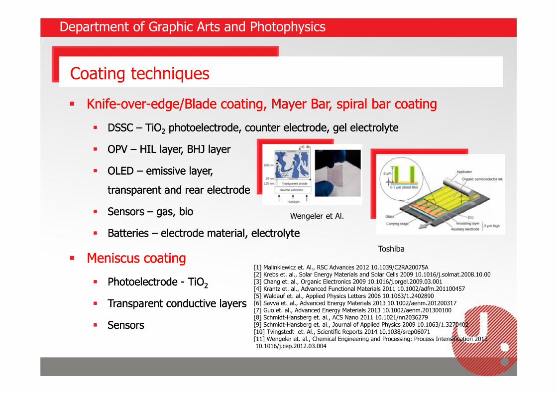
Knife-over-edge/Blade coating, Mayer Bar, spiral bar coating DSSC – TiO2 photoelectrode, counter electrode, gel electrolyte
OPV – HIL layer, BHJ layer
OLED – emissive layer, transparent and rear electrode
Sensors – gas, bio
Batteries – electrode material, electrolyte
Meniscus coating Photoelectrode - TiO2
Transparent conductive layers
Sensors
Coating techniques
Department of Graphic Arts and Photophysics
Toshiba
[1] Malinkiewicz et. Al., RSC Advances 2012 10.1039/C2RA20075A[2] Krebs et. al., Solar Energy Materials and Solar Cells 2009 10.1016/j.solmat.2008.10.00[3] Chang et. al., Organic Electronics 2009 10.1016/j.orgel.2009.03.001[4] Krantz et. al., Advanced Functional Materials 2011 10.1002/adfm.201100457[5] Waldauf et. al., Applied Physics Letters 2006 10.1063/1.2402890[6] Savva et. al., Advanced Energy Materials 2013 10.1002/aenm.201200317[7] Guo et. al., Advanced Energy Materials 2013 10.1002/aenm.201300100[8] Schmidt-Hansberg et. al., ACS Nano 2011 10.1021/nn2036279[9] Schmidt-Hansberg et. al., Journal of Applied Physics 2009 10.1063/1.3270402[10] Tvingstedt et. Al., Scientific Reports 2014 10.1038/srep06071[11] Wengeler et. al., Chemical Engineering and Processing: Process Intensification 201310.1016/j.cep.2012.03.004
Wengeler et Al.

Slot Die
Curtain coating
Multiple slot
Slide coating
Slot Die
Curtain coating
Multiple slot
Slide coating
Coating techniques
Department of Graphic Arts and Photophysics
Media Format R2R, SheetsInk Waste LowCoating Speed 100- 500 m.min-1
Ink Viscosity 10-25 000 mPa.sWet Thickness 5-500 µmDry Thickness 0.01-100 µmResolution Given by shim
Schmitt et Al.www.packaging-int.com
plasticphotovoltaics.org

Coating techniques applications
Department of Graphic Arts and Photophysics
Hwang et Al.
OPV – transparent electrode, BHJ layers(P3HT:PCBM), ETL
Lamination adhesives – pressure sensitive
HTL (PEDOT:PSS), ETL layers (TiO2, ZnO)
Electrochromic display
OLED – PLED – emissive layers, HIL layers, ETL
Battery – electrode layers, collectors
OPV – transparent electrode, BHJ layers(P3HT:PCBM), ETL
Lamination adhesives – pressure sensitive
HTL (PEDOT:PSS), ETL layers (TiO2, ZnO)
Electrochromic display
OLED – PLED – emissive layers, HIL layers, ETL
Battery – electrode layers, collectors
[1] Krebs et. al., Solar Energy Materials and Solar Cells 2009 10.1016/j.solmat.2008.10.004[2] Han et. al., Journal of Coatings Technology and Research 2014 10.1007/s11998-013-9485-3[3] Krebs et. al., Solar Energy Materials and Solar Cells 2009 10.1016/j.solmat.2008.12.012[4] Huang et. al., Journal of Applied Polymer Science 2013 10.1002/app.38617[5] Chang et. al., Polymer Engineering & Science 2009 10.1002/pen.21360[6] Lin et. al., Advances in Polymer Technology 2013 10.1002/adv.21271[7] Tracton, Coatings Technology: Fundamentals, Testing, and Processing Techniques[8] Kistler, Liquid Film Coating.[9] Krebs et. al., Organic Electronics 2009 10.1016/j.orgel.2009.03.009[10] Angmo et. al., Solar Energy Materials and Solar Cells 2012 10.1016/j.solmat.2012.07.004[11] Wengeler et. al., Journal of Coatings Technology and Research 2014 10.1007/s11998-013-9483-5[12] Jakubka et. al., Solar Energy Materials and Solar Cells 2013 10.1016/j.solmat.2012.10.007[13] Alstrup et. al., ACS Applied Materials & Interfaces 2010 10.1021/am100505e
Frontier

+ High uniformity of layers
+ Deposition to 3D object
+ Relatively high rangeof thickness of layers
+ High uniformity of layers
+ Deposition to 3D object
+ Relatively high rangeof thickness of layers
Department of Graphic Arts and Photophysics
Media Format Sheets, R2RInk Waste moderateCoating Speed Up to 100 m.min-1
Ink Viscosity 10-1000 mPa.sWet Thickness 1-500 µmDry Thickness 0.01-100 µmResolution Tech. Sol. dependent
– Ink Waste
– Complicated patterning
– Low resolution of patterning
– Ink Waste
– Complicated patterning
– Low resolution of patterning
Coating techniques – Spray Coating
Sono-tek

OPV - HIL, BHJ, ETL
Transparent conductive layers (CNT,PEDOT:PSS, PANI:HCl)
Memory
OFET
Battery
OLED
OPV - HIL, BHJ, ETL
Transparent conductive layers (CNT,PEDOT:PSS, PANI:HCl)
Memory
OFET
Battery
OLED
Department of Graphic Arts and Photophysics
Coating techniques – Spray Coating
Sono-tek[1] Green et. al., Applied Physics Letters 2008 10.1063/1.2836267[2] Steirer et. al., Solar Energy Materials and Solar Cells 2009 10.1016/j.solmat.2008.10.026[3] Zhao et. al., Journal of Bionanoscience 2012 10.1166/rnn.2012.1011[4] Girotto et. al., Solar Energy Materials and Solar Cells 2009 10.1016/j.solmat.2008.11.052[5] Girotto et. al., Advanced Functional Materials 2011 10.1002/adfm.201001562[6] Kang et. al., Solar Energy Materials and Solar Cells 2012 10.1016/j.solmat.2012.04.027[7] Lewis et. al., Solar Energy Materials and Solar Cells 2011 10.1016/j.solmat.2011.05.037[8] Colella et. al., Applied Physics Letters 2013 10.1063/1.4807464[9] Ishikawa et. al., Applied Physics Letters 2004 10.1063/1.1690493[10] Vak et. al., Applied Physics Letters 2007 10.1063/1.2772766[11] Yu et. al., IEEE Journal of Selected Topics in Quantum Electronics 2010 10.1109/JSTQE.2010.2042282
Singh at Al.
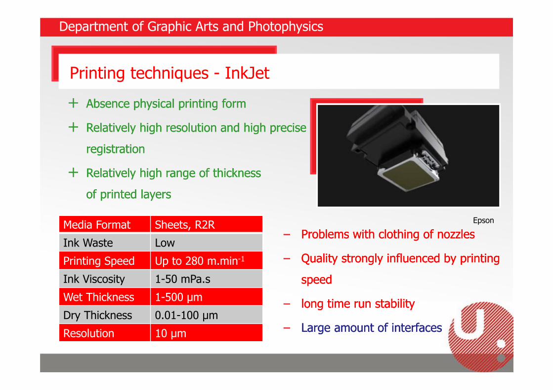
+ Absence physical printing form
+ Relatively high resolution and high preciseregistration
+ Relatively high range of thicknessof printed layers
+ Absence physical printing form
+ Relatively high resolution and high preciseregistration
+ Relatively high range of thicknessof printed layers
Department of Graphic Arts and Photophysics
Coatema
Media Format Sheets, R2RInk Waste LowPrinting Speed Up to 280 m.min-1
Ink Viscosity 1-50 mPa.sWet Thickness 1-500 µmDry Thickness 0.01-100 µmResolution 10 µm
Printing techniques - InkJet
– Problems with clothing of nozzles
– Quality strongly influenced by printing speed
– long time run stability
– Large amount of interfaces
– Problems with clothing of nozzles
– Quality strongly influenced by printing speed
– long time run stability
– Large amount of interfaces
Epson

BHJ, ETL (PFN, ZnO,TiO2), HTL (PEDOT:PSS, MoO3)
Transparent conductor (Ag nanowire, CNT, SWCNT, Graphene, ITO, AZO, ATO)
Sensors Catalytic layers Conductive (Ag, Cu), semiconductive,
dielectric layers for several type of devices Transistors – OFET, OECT OPV, DSSC OLED – POLED, SMOLED Piezoelectric elements –
micropumps, tactile Baterries, supercapacitors Memory Reactive colors
Department of Graphic Arts and Photophysics
Printing techniques - InkJet
Holst Centre
[1] Derby et. al., Annual Review of Materials Research 2010 10.1146/annurev-matsci-070909-104502[2] de Gans et. al., Advanced Materials 2004 10.1002/adma.200300385[3] Magdassi, The Chemistry of Inkjet Inks[4] Soltman et. al., Langmuir 2008 10.1021/la7026847[5] Kang et. al., Thin Solid Films 2010 10.1016/j.tsf.2009.10.126[6] Deegan et. al., Nature 1997 10.1038/39827[7] Eom et. al., Organic Electronics 2010 10.1016/j.orgel.2010.06.007[8] Lange et. al., Journal of Nanoscience and Nanotechnology 2013 10.1166/jnn.2013.7500[9] Angmo et. al., Advanced Energy Materials 2013 10.1002/aenm.201201050[10] van Franeker et. al., Solar Energy Materials and Solar Cells 2013 10.1016/j.solmat.2013.06.033[11] Lange et. al., Solar Energy Materials and Solar Cells 2013 10.1016/j.solmat.2012.10.011[12] Eom et. al., Organic Electronics 2009 10.1016/j.orgel.2009.01.015[13] Galagan et. al., Solar Energy Materials and Solar Cells 2012 10.1016/j.solmat.2012.04.039[14] Huang et. al., Organic Electronics 2013 10.1016/j.orgel.2013.08.001[15] Yu et. al., Nanoscale 2012 10.1039/c2nr31508d

+ Most used production technique
+ Variety of thickness of layers
+ Relatively easy preparation of stencil
+ Most used production technique
+ Variety of thickness of layers
+ Relatively easy preparation of stencil
Department of Graphic Arts and Photophysics
Media Format Sheets, R2RInk Waste LowPrinting Speed Up to 50 m.min-1
Ink Viscosity 100-20 000 mPa.sWet Thickness 3-1000 µmDry Thickness 0.02-1000 µmResolution 6 µm
Printing techniques – Screen printing
– Printing speed, high viscosity– Printing speed, high viscosity CoatemaKuroda
3D-Micromac AG

Department of Graphic Arts and Photophysics
Printing techniques – Screen Printing Photocathode (TiO2, ZnO, etc.) Counter electrode (PEDOT:PSS, PANI,
PPY, CNT, Graphene, Ag) Conductive patterns (Ag, Cu) Electrolytes BHJ layers, ETL, HTL Sealing layers, Barrier layers Sensors Catalytic layers Conductivee, (Semi)conductive,
dielectric layers for several type of devices Transistors – OFET, OECT OPV, DSSC OLED – POLED, SMOLED Batteries, supercapacitors Memory Reactive colors Piezoelectric elements – micropumps, tactile
Photocathode (TiO2, ZnO, etc.) Counter electrode (PEDOT:PSS, PANI,
PPY, CNT, Graphene, Ag) Conductive patterns (Ag, Cu) Electrolytes BHJ layers, ETL, HTL Sealing layers, Barrier layers Sensors Catalytic layers Conductivee, (Semi)conductive,
dielectric layers for several type of devices Transistors – OFET, OECT OPV, DSSC OLED – POLED, SMOLED Batteries, supercapacitors Memory Reactive colors Piezoelectric elements – micropumps, tactile
Plasticphotovoltaic.org
[1] Riemer et. al., Microelectronics International 1989 10.1108/eb044350[2] Krebs et. al., Solar Energy Materials and Solar Cells 2009 10.1016/j.solmat.2008.10.004[3] Kipphan, Handbook of Print Media - Technologies and Production Methods[4] Zhang et. al., Japanese Journal of Applied Physics 2009 10.1143/JJAP.48.020208[5] Krebs et. al., Solar Energy Materials and Solar Cells 2011 10.1016/j.solmat.2010.11.007[6] Sommer-Larsen et. al., Energy Technology 2013 10.1002/ente.201200055[7] Krebs et. al., Advanced Materials 2014 10.1002/adma.201302031[8] Galagan et. al., Solar Energy Materials and Solar Cells 2011 10.1016/j.solmat.2010.08.011

+ Very stable printing process
+ Highest printing quality
+ High printing speed
+ Printing form resistant to solvents
+ Reverse gravure for precise coating
+ Very stable printing process
+ Highest printing quality
+ High printing speed
+ Printing form resistant to solvents
+ Reverse gravure for precise coating
Department of Graphic Arts and Photophysics
Media Format Sheets, R2RInk Waste LowPrinting Speed Up to 500 m.min-1
Ink Viscosity 10-20 000 mPa.sWet Thickness 5-80 µmDry Thickness 0.02-80 µmResolution 3 µm
Printing techniques – Gravure
– Expensive printing form/ cyllinder
– Mainly gravureis suited to flexible substrates
– Expensive printing form/ cyllinder
– Mainly gravureis suited to flexible substrates
www.iggesund.com
3D-Micromac AG

HIL (MoO3, PEDOT:PSS), BHJ ETL (ZnO2, TiO2) Conductive tracks (Ag, Cu) Dielectrics OLED – SMOLED, PLED – emissive layer OFET – ID structures, Dielectric layer,
Semiconductor layer, RFID antenas Sensors – RH, Biosensing layer Voltage multiplier circuits Memory Antistatic layers Microfluidic chanells
HIL (MoO3, PEDOT:PSS), BHJ ETL (ZnO2, TiO2) Conductive tracks (Ag, Cu) Dielectrics OLED – SMOLED, PLED – emissive layer OFET – ID structures, Dielectric layer,
Semiconductor layer, RFID antenas Sensors – RH, Biosensing layer Voltage multiplier circuits Memory Antistatic layers Microfluidic chanells
Department of Graphic Arts and Photophysics
Printing techniques – Gravure
VTT
[1] Välimäki et. Al., Nanoscale, 2015 10.1039/C5NR00204D[2] Noh et. al., IEEE Electron Device Letters 2011 10.1109/LED.2011.2165695[3] de la Fuente Vornbrock et. al., Organic Electronics 2010 10.1016/j.orgel.2010.09.003[4] Shin et. al., Journal of Materials Chemistry 2012 10.1039/c2jm30198a[5] Kopola et. al., Solar Energy Materials and Solar Cells 2011
10.1016/j.solmat.2010.12.020
CSEM
[6] Kopola et. al., Solar Energy Materials and Solar Cells 2010 10.1016/j.solmat.2010.05.027[7] Koidis et. al., Solar Energy Materials and Solar Cells 2013 10.1016/j.solmat.2012.12.044[8] Voigt et. al., Solar Energy Materials and Solar Cells 2011 10.1016/j.solmat.2010.10.013[9] Sung et. al., IEEE Transactions on Components and Packaging Technologies
2010 10.1109/TCAPT.2009.2021464
VTT
Välimäki et Al.

+ Stable printing process
+ High printing speed
+ Rigid and flexible substrates
+ Relatively inexpensive printing form
+ Stable printing process
+ High printing speed
+ Rigid and flexible substrates
+ Relatively inexpensive printing form
Department of Graphic Arts and Photophysics
Media Format Sheets, R2RInk Waste LowPrinting Speed Up to 1000 m.min-1
Ink Viscosity 10 -1 000 mPa.sWet Thickness 5 - 30 µmDry Thickness 0.03 - 10 µmResolution 30 µm
Printing techniques – Flexography
– Limited thickness of layers
– Uniformity of topology of fine lines
– NIP pressure is crucial
– Limited thickness of layers
– Uniformity of topology of fine lines
– NIP pressure is crucial
Altana
Simec Group

Conductive interconnection, Transparent conducive layers
(CNT, PEDOT:PSS), conductive grids HTL (PEDOT:PSS, V2O5) RFID antennas Biostatic layers Dielectric layers (OFET, RFID) Laudspeakers Fuid-guiding channels Drug delivery systems
Conductive interconnection, Transparent conducive layers
(CNT, PEDOT:PSS), conductive grids HTL (PEDOT:PSS, V2O5) RFID antennas Biostatic layers Dielectric layers (OFET, RFID) Laudspeakers Fuid-guiding channels Drug delivery systems
Department of Graphic Arts and Photophysics
Printing techniques – Flexography
Syrovy
[1] Leppäniemi et. Al., Adv. Mater. 27, 7168–7175 (2015).[2] Hübler et. al., Advanced Energy Materials 2011 10.1002/aenm.201100394[3] Hösel et. al., Energy Technology 2013 10.1002/ente.201200029[4] Krebs et. al., Advanced Materials 2014 10.1002/adma.201302031[5] Deganello et. al., Thin Solid Films 2010 10.1016/j.tsf.2010.05.125[6] Mo et. al., Nanotechnology 2016, 10.1088/0957-4484/27/6/065202[7] Carlé et. Al., Energy Materials and Solar Cells 2013 10.1016/j.solmat.2012.09.008[8] Kololuoma et. Al., Oxide-based Materials and Devices VI 2015 doi: 10.1117/12.2079270[9] Keng et. Al., IEEE 13th Electronics Packaging Technology Conference 2011, 10.1109/EPTC.2011.6184475 Plasticphotovoltaics.org
200 m/min
+ Rigid and flexible substrates
+ Printability of 3D surface
+ Printing quality
+ Printing speed
+ Rigid and flexible substrates
+ Printability of 3D surface
+ Printing quality
+ Printing speed
Department of Graphic Arts and Photophysics
Media Format Sheets, R2RInk Waste LowPrinting Speed Up to 120000 parts/hrInk Viscosity 10 -1000 mPa.sWet Thickness 5- 80 µmDry Thickness 0.05 - 20 µmResolution 25 µm
Printing techniques – Pad printing, offset gravure
TRI Elektronik
Tampoprint
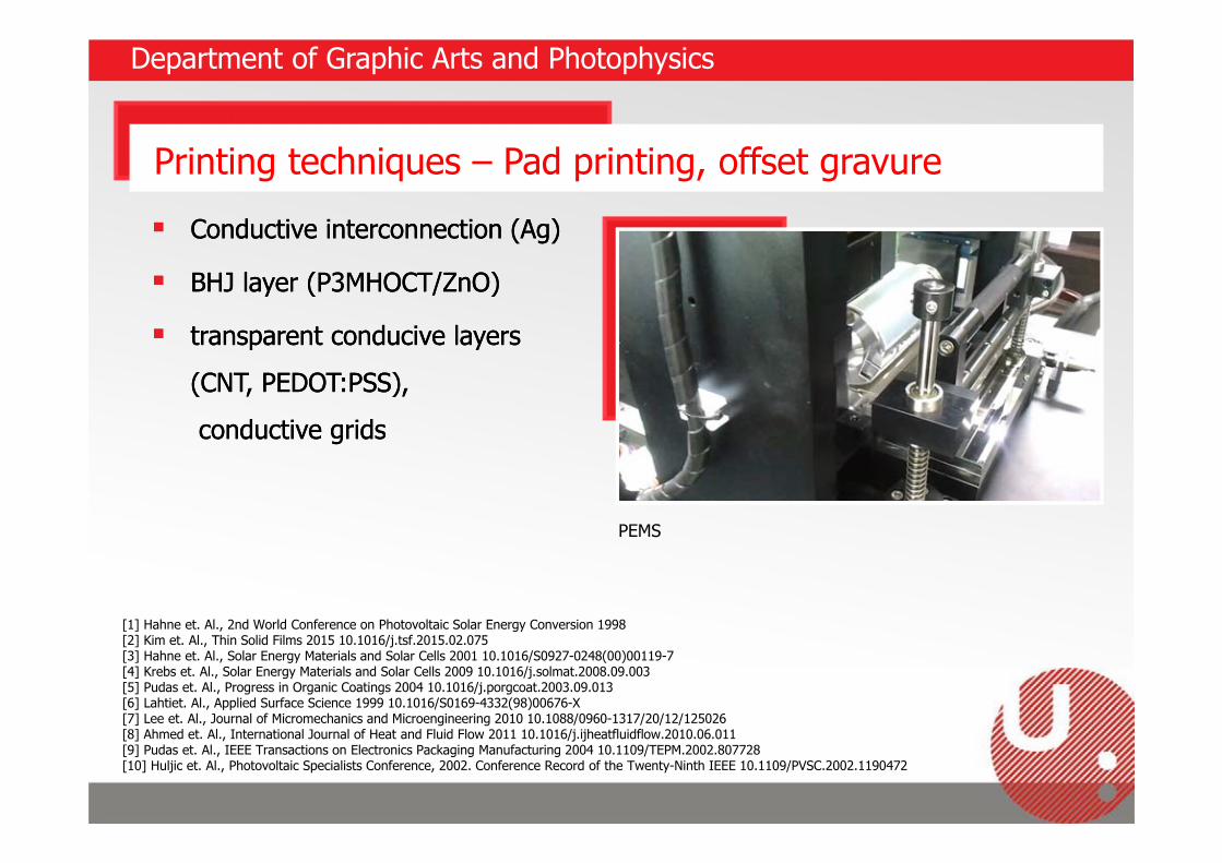
Conductive interconnection (Ag)
BHJ layer (P3MHOCT/ZnO)
transparent conducive layers(CNT, PEDOT:PSS),conductive grids
Conductive interconnection (Ag)
BHJ layer (P3MHOCT/ZnO)
transparent conducive layers(CNT, PEDOT:PSS),conductive grids
Department of Graphic Arts and Photophysics
Printing techniques – Pad printing, offset gravure
[1] Hahne et. Al., 2nd World Conference on Photovoltaic Solar Energy Conversion 1998[2] Kim et. Al., Thin Solid Films 2015 10.1016/j.tsf.2015.02.075[3] Hahne et. Al., Solar Energy Materials and Solar Cells 2001 10.1016/S0927-0248(00)00119-7[4] Krebs et. Al., Solar Energy Materials and Solar Cells 2009 10.1016/j.solmat.2008.09.003[5] Pudas et. Al., Progress in Organic Coatings 2004 10.1016/j.porgcoat.2003.09.013 [6] Lahtiet. Al., Applied Surface Science 1999 10.1016/S0169-4332(98)00676-X[7] Lee et. Al., Journal of Micromechanics and Microengineering 2010 10.1088/0960-1317/20/12/125026[8] Ahmed et. Al., International Journal of Heat and Fluid Flow 2011 10.1016/j.ijheatfluidflow.2010.06.011[9] Pudas et. Al., IEEE Transactions on Electronics Packaging Manufacturing 2004 10.1109/TEPM.2002.807728 [10] Huljic et. Al., Photovoltaic Specialists Conference, 2002. Conference Record of the Twenty-Ninth IEEE 10.1109/PVSC.2002.1190472
PEMS

+ Printing speed
+ High resolution
+ inexpensive printing plates fabrication
+ Frequently used printing technique
+ Printing speed
+ High resolution
+ inexpensive printing plates fabrication
+ Frequently used printing technique
Department of Graphic Arts and Photophysics
Media Format Sheets, R2RInk Waste LowPrinting Speed Up to 1000 m.min-1
Ink Viscosity 10 -100 Pa.sWet Thickness 10 µmDry Thickness 3 µmResolution 25 µm
Printing techniques – Offset printing
– Limited thickness of layers
– High resistivity of conductive layers
– Lack of commercial functional ink
– Limited thickness of layers
– High resistivity of conductive layers
– Lack of commercial functional ink
Kim
www.brancher.com

OFET ID structures
Conductive circuits
Passive components
Sensors
Thermochromic display
Battery
OPV
OFET ID structures
Conductive circuits
Passive components
Sensors
Thermochromic display
Battery
OPV
Department of Graphic Arts and Photophysics
Printing techniques – Offset printing
Brunel University
Brunel University

Nanoimprinting lithography NIL
Soft Lithography Microcontact Printig µCP
Micromolding in Capillaries MIMIC
Nanotransfer printing nTP
Replica molding REM
Microtransfer molding µTM
Solvent-assisted micromolding SAMIM
Nanoimprinting lithography NIL
Soft Lithography Microcontact Printig µCP
Micromolding in Capillaries MIMIC
Nanotransfer printing nTP
Replica molding REM
Microtransfer molding µTM
Solvent-assisted micromolding SAMIM
Department of Graphic Arts and Photophysics
Others „printing“ techniques for µ-Patterning
www.miplaza.com
OKNANOLAB
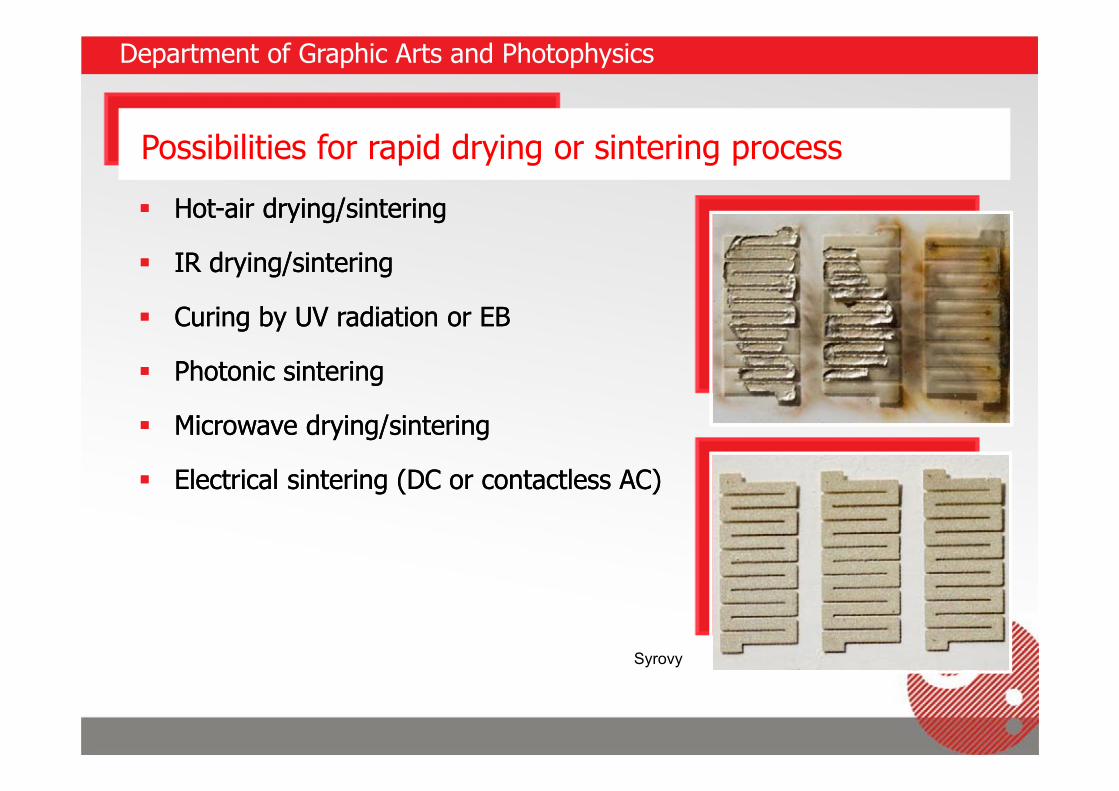
Hot-air drying/sintering
IR drying/sintering
Curing by UV radiation or EB
Photonic sintering
Microwave drying/sintering
Electrical sintering (DC or contactless AC)
Hot-air drying/sintering
IR drying/sintering
Curing by UV radiation or EB
Photonic sintering
Microwave drying/sintering
Electrical sintering (DC or contactless AC)
Possibilities for rapid drying or sintering process
Department of Graphic Arts and Photophysics
Syrovy

Thank you for your attention
Department of Graphic Arts and Photophysics