switchmode power supply reference manual - on semi
TRANSCRIPT

Switch−Mode Power Supply
Reference Manual
SMPSRM/DRev. 4, Apr−2014
© SCILLC, 2014Previous Edition © 2002“All Rights Reserved’’

SMPSRM
www.onsemi.com 2
ON Semiconductor and are registered trademarks of Semiconductor Components Industries, LLC (SCILLC). SCILLC owns the rights to a number of patents, trademarks,copyrights, trade secrets, and other intellectual property. A listing of SCILLC’s product/patent coverage may be accessed at www.onsemi.com/site/pdf/Patent−Marking.pdf. SCILLCreserves the right to make changes without further notice to any products herein. SCILLC makes no warranty, representation or guarantee regarding the suitability of its products for anyparticular purpose, nor does SCILLC assume any liability arising out of the application or use of any product or circuit, and specifically disclaims any and all liability, including withoutlimitation special, consequential or incidental damages. “Typical” parameters which may be provided in SCILLC data sheets and/or specifications can and do vary in different applicationsand actual performance may vary over time. All operating parameters, including “Typicals” must be validated for each customer application by customer’s technical experts. SCILLCdoes not convey any license under its patent rights nor the rights of others. SCILLC products are not designed, intended, or authorized for use as components in systems intended forsurgical implant into the body, or other applications intended to support or sustain life, or for any other application in which the failure of the SCILLC product could create a situation wherepersonal injury or death may occur. Should Buyer purchase or use SCILLC products for any such unintended or unauthorized application, Buyer shall indemnify and hold SCILLC andits officers, employees, subsidiaries, affiliates, and distributors harmless against all claims, costs, damages, and expenses, and reasonable attorney fees arising out of, directly or indirectly,any claim of personal injury or death associated with such unintended or unauthorized use, even if such claim alleges that SCILLC was negligent regarding the design or manufactureof the part. SCILLC is an Equal Opportunity/Affirmative Action Employer. This literature is subject to all applicable copyright laws and is not for resale in any manner.
PUBLICATION ORDERING INFORMATIONN. American Technical Support: 800−282−9855 Toll FreeUSA/Canada
Europe, Middle East and Africa Technical Support:Phone: 421 33 790 2910
Japan Customer Focus CenterPhone: 81−3−5817−1050
LITERATURE FULFILLMENT:Literature Distribution Center for ON SemiconductorP.O. Box 5163, Denver, Colorado 80217 USAPhone: 303−675−2175 or 800−344−3860 Toll Free USA/CanadaFax: 303−675−2176 or 800−344−3867 Toll Free USA/CanadaEmail: [email protected]
ON Semiconductor Website: www.onsemi.com
Order Literature: http://www.onsemi.com/orderlit
For additional information, please contact your localSales Representative

SMPSRM
www.onsemi.com 3
Forward
Every new electronic product, except those that are battery powered, requires converting off−line115 Vac or 230 Vac power to some dc voltage for powering the electronics. The availability of designand application information and highly integrated semiconductor control ICs for switching powersupplies allows the designer to complete this portion of the system design quickly and easily.Whether you are an experienced power supply designer, designing your first switching powersupply or responsible for a make or buy decision for power supplies, the variety of informationin the Switch−Mode Power Supply Reference Manual should prove useful.
This reference manual contains useful background information on switching power supplies forthose who want to have more meaningful discussions and are not necessarily experts on powersupplies. It also provides real SMPS examples, and identifies several application notes andadditional design resources available from ON Semiconductor, as well as helpful books availablefrom various publishers and useful web sites for those who are experts and want to increase theirexpertise. An extensive list and brief description of analog ICs, power transistors, rectifiers and otherdiscrete components available from ON Semiconductor for designing a SMPS are also provided.
For the latest updates and additional information on energy efficient power management and discretedevices, please visit our website at www.onsemi.com.
Soft−Skip is a trademark of Semiconductor Components Industries, LLC. ENERGY STAR is a registered mark U.S. mark. All brandnames and product names appearing in this document are registered trademarks or trademarks of their respective holders.

SMPSRM
www.onsemi.com 4
Table of ContentsPage
Introduction 5. . . . . . . . . . . . . . . . . . . . . . . . . . . . . . . . . . . . . . . . . . . . . . . . . . . . . . . . . . . . . . . . . . . . . . . . . . . . . . . . .Linear versus Switching Power Supplies 5. . . . . . . . . . . . . . . . . . . . . . . . . . . . . . . . . . . . . . . . . . . . . . . . . . . . . . . . . . .Switching Power Supply Fundamentals 5. . . . . . . . . . . . . . . . . . . . . . . . . . . . . . . . . . . . . . . . . . . . . . . . . . . . . . . . . . .
The Forward−Mode Converter 5. . . . . . . . . . . . . . . . . . . . . . . . . . . . . . . . . . . . . . . . . . . . . . . . . . . . . . . . . . . . . . . .The Flyback−Mode Converter 7. . . . . . . . . . . . . . . . . . . . . . . . . . . . . . . . . . . . . . . . . . . . . . . . . . . . . . . . . . . . . . . .
Common Switching Power Supply Topologies 8. . . . . . . . . . . . . . . . . . . . . . . . . . . . . . . . . . . . . . . . . . . . . . . . . . . . . .Interleaved Multiphase Converters 13. . . . . . . . . . . . . . . . . . . . . . . . . . . . . . . . . . . . . . . . . . . . . . . . . . . . . . . . . . . . . .Selecting the Method of Control 14. . . . . . . . . . . . . . . . . . . . . . . . . . . . . . . . . . . . . . . . . . . . . . . . . . . . . . . . . . . . . . . .The Choice of Semiconductors 16. . . . . . . . . . . . . . . . . . . . . . . . . . . . . . . . . . . . . . . . . . . . . . . . . . . . . . . . . . . . . . . . .
Power Switches 16. . . . . . . . . . . . . . . . . . . . . . . . . . . . . . . . . . . . . . . . . . . . . . . . . . . . . . . . . . . . . . . . . . . . . . . . . . .The Bipolar Power Transistor 16. . . . . . . . . . . . . . . . . . . . . . . . . . . . . . . . . . . . . . . . . . . . . . . . . . . . . . . . . . . . . . . . . .The Power MOSFET 17. . . . . . . . . . . . . . . . . . . . . . . . . . . . . . . . . . . . . . . . . . . . . . . . . . . . . . . . . . . . . . . . . . . . . . . . .
Driving MOSFETs in Switching Power Supply Applications 18. . . . . . . . . . . . . . . . . . . . . . . . . . . . . . . . . . . . . . .The Insulated Gate Bipolar Transistor (IGBT) 19. . . . . . . . . . . . . . . . . . . . . . . . . . . . . . . . . . . . . . . . . . . . . . . . . . . . .
Rectifiers 19. . . . . . . . . . . . . . . . . . . . . . . . . . . . . . . . . . . . . . . . . . . . . . . . . . . . . . . . . . . . . . . . . . . . . . . . . . . . . . . .The Magnetic Components 21. . . . . . . . . . . . . . . . . . . . . . . . . . . . . . . . . . . . . . . . . . . . . . . . . . . . . . . . . . . . . . . . . . . .Laying Out the Printed Circuit Board 21. . . . . . . . . . . . . . . . . . . . . . . . . . . . . . . . . . . . . . . . . . . . . . . . . . . . . . . . . . . .Losses and Stresses in Switching Power Supplies 24. . . . . . . . . . . . . . . . . . . . . . . . . . . . . . . . . . . . . . . . . . . . . . . . . . .Techniques to Improve Efficiency in Switching Power Supplies 25. . . . . . . . . . . . . . . . . . . . . . . . . . . . . . . . . . . . . . .
The Synchronous Rectifier 25. . . . . . . . . . . . . . . . . . . . . . . . . . . . . . . . . . . . . . . . . . . . . . . . . . . . . . . . . . . . . . . . . .Snubbers and Clamps 27. . . . . . . . . . . . . . . . . . . . . . . . . . . . . . . . . . . . . . . . . . . . . . . . . . . . . . . . . . . . . . . . . . . . . .The Lossless Snubber 28. . . . . . . . . . . . . . . . . . . . . . . . . . . . . . . . . . . . . . . . . . . . . . . . . . . . . . . . . . . . . . . . . . . . . .The Active Clamp 29. . . . . . . . . . . . . . . . . . . . . . . . . . . . . . . . . . . . . . . . . . . . . . . . . . . . . . . . . . . . . . . . . . . . . . . . .Quasi−Resonant Topologies 30. . . . . . . . . . . . . . . . . . . . . . . . . . . . . . . . . . . . . . . . . . . . . . . . . . . . . . . . . . . . . . . . .
Power Factor Correction 32. . . . . . . . . . . . . . . . . . . . . . . . . . . . . . . . . . . . . . . . . . . . . . . . . . . . . . . . . . . . . . . . . . . . . .
Topology Overview 35. . . . . . . . . . . . . . . . . . . . . . . . . . . . . . . . . . . . . . . . . . . . . . . . . . . . . . . . . . . . . . . . . . . . . . . . . .
SMPS Examples 51. . . . . . . . . . . . . . . . . . . . . . . . . . . . . . . . . . . . . . . . . . . . . . . . . . . . . . . . . . . . . . . . . . . . . . . . . . . . .
Additional Documentation Available from ON Semiconductor 67. . . . . . . . . . . . . . . . . . . . . . . . . . . . . . . . . . . . . . . .Design Notes 67. . . . . . . . . . . . . . . . . . . . . . . . . . . . . . . . . . . . . . . . . . . . . . . . . . . . . . . . . . . . . . . . . . . . . . . . . . . . .Tutorials 68. . . . . . . . . . . . . . . . . . . . . . . . . . . . . . . . . . . . . . . . . . . . . . . . . . . . . . . . . . . . . . . . . . . . . . . . . . . . . . . .Application Notes 69. . . . . . . . . . . . . . . . . . . . . . . . . . . . . . . . . . . . . . . . . . . . . . . . . . . . . . . . . . . . . . . . . . . . . . . . .

SMPSRM
www.onsemi.com 5
IntroductionThe never−ending drive towards smaller and lighter
products poses severe challenges for the power supplydesigner. In particular, disposing of excess heatgenerated by power semiconductors is becoming moreand more difficult. Consequently it is important that thepower supply be as small and as efficient as possible, andover the years power supply engineers have responded tothese challenges by steadily reducing the size andimproving the efficiency of their designs.
Switching power supplies offer not only higherefficiencies but also greater flexibility to the designer.Recent advances in semiconductor, magnetic and passivetechnologies make the switching power supply an evermore popular choice in the power conversion arena.
This guide is designed to give the prospective designeran overview of the issues involved in designingswitchmode power supplies. It describes the basicoperation of the more popular topologies of switchingpower supplies, their relevant parameters, providescircuit design tips, and information on how to select themost appropriate semiconductor and passivecomponents. The guide also lists the ON Semiconductorcomponents expressly built for use in switching powersupplies.
Linear versus SwitchingPower Supplies
Switching and linear regulators use fundamentallydifferent techniques to produce a regulated outputvoltage from an unregulated input. Each technique hasadvantages and disadvantages, so the application willdetermine the most suitable choice.
Linear power supplies can only step−down an inputvoltage to produce a lower output voltage. This is doneby operating a bipolar transistor or MOSFET pass unit inits linear operating mode; that is, the drive to the pass unitis proportionally changed to maintain the required outputvoltage. Operating in this mode means that there isalways a headroom voltage, Vdrop, between the inputand the output. Consequently the regulator dissipates aconsiderable amount of power, given by (Vdrop Iload).
This headroom loss causes the linear regulator to onlybe 35 to 65 percent efficient. For example, if a 5.0 Vregulator has a 12 V input and is supplying 100 mA, itmust dissipate 700 mW in the regulator in order to deliver500 mW to the load , an efficiency of only 42 percent.The cost of the heatsink actually makes the linearregulator uneconomical above 10 watts for smallapplications. Below that point, however, linearregulators are cost−effective in step−down applications.
A low drop−out (LDO) regulator uses an improvedoutput stage that can reduce Vdrop to considerably lessthan 1.0 V. This increases the efficiency and allows thelinear regulator to be used in higher power applications.
Designing with a linear regulator is simple and cheap,requiring few external components. A linear design isconsiderably quieter than a switcher since there is nohigh−frequency switching noise.
Switching power supplies operate by rapidly switchingthe pass units between two efficient operating states: cutoff, where there is a high voltage across the pass unitbut no current flow; and saturation, where there is a highcurrent through the pass unit but at a very small voltagedrop. Essentially, the semiconductor power switchcreates an AC voltage from the input DC voltage. ThisAC voltage can then be stepped−up or down bytransformers and then finally filtered back to DC at itsoutput. Switching power supplies are much moreefficient, ranging from 65 to 95 percent.
The downside of a switching design is that it isconsiderably more complex. In addition, the outputvoltage contains switching noise, which must beremoved for many applications.
Although there are clear differences between linearand switching regulators, many applications require bothtypes to be used. For example, a switching regulator mayprovide the initial regulation, then a linear regulator mayprovide post−regulation for a noise−sensitive part of thedesign, such as a sensor interface circuit.
Switching Power SupplyFundamentals
There are two basic types of pulse−width modulated(PWM) switching power supplies, forward−mode andboost−mode. They differ in the way the magneticelements are operated. Each basic type has its advantagesand disadvantages.
The Forward−Mode ConverterThe forward−mode converter can be recognized by the
presence of an L−C filter on its output. The L−C filtercreates a DC output voltage, which is essentially thevolt−time average of the L−C filter’s input ACrectangular waveform. This can be expressed as:
Vout � Vin � duty cycle (eq. 1)
The switching power supply controller varies the dutycycle of the input rectangular voltage waveform and thuscontrols the signal’s volt−time average.
The buck or step−down converter is the simplestforward−mode converter, which is shown in Figure 1.
SMPSRM
www.onsemi.com 6
Ipk
TIME
Iload
Imin
PowerSwitch
OFF
PowerSwitch
OFFPowerSwitch
ON
PowerSwitch
ON
Vsat
Power SW Power SW DiodeDiodeTIME
Figure 1. A Basic Forward−Mode Converter and Waveforms (Buck Converter Shown)
Vfwd
IND
UC
TO
R C
UR
RE
NT
(AM
PS
)D
IOD
E V
OLT
AG
E(V
OLT
S)
LO
RloadCoutDVin
SW
Ion Ioff
Its operation can be better understood when it is brokeninto two time periods: when the power switch is turnedon and turned off. When the power switch is turned on,the input voltage is directly connected to the input of theL−C filter. Assuming that the converter is in asteady−state, there is the output voltage on the filter’soutput. The inductor current begins a linear ramp from aninitial current dictated by the remaining flux in theinductor. The inductor current is given by:
iL(on) �(Vin � Vout)
Lt � iinit 0 � t � ton (eq. 2)
During this period, energy is stored as magnetic fluxwithin the core of the inductor. When the power switchis turned off, the core contains enough energy to supplythe load during the following off period plus somereserve energy.
When the power switch turns off, the voltage on theinput side of the inductor tries to fly below ground, but is
clamped when the catch diode D becomes forwardbiased. The stored energy then continues flowing to theoutput through the catch diode and the inductor. Theinductor current decreases from an initial value ipk and isgiven by:
iL(off) � ipk �Voutt
L0 � t � toff (eq. 3)
The off period continues until the controller turns thepower switch back on and the cycle repeats itself.
The buck converter is capable of over one kilowatt ofoutput power, but is typically used for on−board regulatorapplications whose output powers are less than 100 watts.Compared to the flyback−mode converter, the forwardconverter exhibits lower output peak−to−peak ripplevoltage. The disadvantage is that it is a step−downtopology only. Since it is not an isolated topology, forsafety reasons the forward converter cannot be used forinput voltages greater than 42.5 VDC.

SMPSRM
www.onsemi.com 7
The Flyback−Mode ConverterThe basic flyback−mode converter uses the same
components as the basic forward−mode converter, but ina different configuration. Consequently, it operates in a
different fashion from the forward−mode converter. Themost elementary flyback−mode converter, the boost orstep−up converter, is shown in Figure 2.
Figure 2. A Basic Boost−Mode Converter and Waveforms (Boost Converter Shown)
PowerSwitch
ON
Vin
PowerSwitch
ON
DiodeON
Vflbk(Vout)
DiodeON
PowerSwitch
ON
TIME
TIME
Ipk
IND
UC
TO
R C
UR
RE
NT
(AM
PS
)S
WIT
CH
VO
LTA
GE
(VO
LTS
)
Iload
Vsat
L
Rload
Cout
D
VinIoff
SWIloadIon
Again, its operation is best understood by considering the“on” and “off” periods separately. When the powerswitch is turned on, the inductor is connected directlyacross the input voltage source. The inductor current thenrises from zero and is given by:
iL(on) �Vint
L� t � 0on (eq. 4)
Energy is stored within the flux in the core of the inductor.The peak current, ipk, occurs at the instant the powerswitch is turned off and is given by:
ipk �Vin ton
L (eq. 5)
When the power switch turns off, the switched side ofthe inductor wants to fly−up in voltage, but is clamped by
the output rectifier when its voltage exceeds the outputvoltage. The energy within the core of the inductor is thenpassed to the output capacitor. The inductor currentduring the off period has a negative ramp whose slope isgiven by:
iL(off) �(Vin � Vout)
L (eq. 6)
The energy is then completely emptied into the outputcapacitor and the switched terminal of the inductor fallsback to the level of the input voltage. Some ringing isevident during this time due to residual energy flowingthrough parasitic elements such as the stray inductancesand capacitances in the circuit.

SMPSRM
www.onsemi.com 8
When there is some residual energy permitted toremain within the inductor core, the operation is called continuous− mode. This can be seen in Figure 3.
Energy for the entire on and off time periods must bestored within the inductor. The stored energy is definedby:
EL � 0.5L � ipk2 (eq. 7)
The boost−mode inductor must store enough energy tosupply the output load for the entire switching period (ton+ toff). Also, boost−mode converters are typically limited
to a 50 percent duty cycle. There must be a time periodwhen the inductor is permitted to empty itself of itsenergy.
The boost converter is used for board−level (i.e.,non−isolated) step−up applications and is limited to lessthan 100−150 watts due to high peak currents. Being anon−isolated converter, it is limited to input voltages ofless than 42.5 VDC. Replacing the inductor with atransformer results in a flyback converter, which may bestep−up or step−down. The transformer also providesdielectric isolation from input to output.
Vsat
DiodeON
Vflbk(Vout)
PowerSwitch
ON
Vin
DiodeON
TIME
TIMEIND
UC
TO
R C
UR
RE
NT
(AM
PS
)S
WIT
CH
VO
LTA
GE
(VO
LTS
)
Figure 3. Waveforms for a Continuous−Mode Boost Converter
PowerSwitch
ON
Ipk
Common Switching Power Supply Topologies
A topology is the arrangement of the power devicesand their magnetic elements. Each topology has its ownmerits within certain applications. There are five majorfactors to consider when selecting a topology for aparticular application. These are:
1. Is input−to−output dielectric isolation required forthe application? This is typically dictated by thesafety regulatory bodies in effect in the region.
2. Are multiple outputs required?3. Does the prospective topology place a reasonable
voltage stress across the power semiconductors?4. Does the prospective topology place a reasonable
current stress upon the power semiconductors?
5. How much of the input voltage is placed acrossthe primary transformer winding or inductor?
Factor 1 is a safety−related issue. Input voltages above42.5 VDC are considered hazardous by the safetyregulatory agencies throughout the world. Therefore,only transformer−isolated topologies must be used abovethis voltage. These are the off−line applications where thepower supply is plugged into an AC source such as a wallsocket.
Multiple outputs require a transformer−basedtopology. The input and output grounds may beconnected together if the input voltage is below42.5 VDC. Otherwise full dielectric isolation is required.

SMPSRM
www.onsemi.com 9
Factors 3, 4 and 5 have a direct affect upon thereliability of the system. Switching power suppliesdeliver constant power to the output load. This power isthen reflected back to the input, so at low input voltages,the input current must be high to maintain the outputpower. Conversely, the higher the input voltage, thelower the input current. The design goal is to place asmuch as possible of the input voltage across thetransformer or inductor so as to minimize the inputcurrent.
Boost−mode topologies have peak currents that areabout twice those found in forward−mode topologies.This makes them unusable at output powers greater than100−150 watts.
Cost is a major factor that enters into the topologydecision. There are large overlaps in the performanceboundaries between the topologies. Sometimes the mostcost−effective choice is to purposely design one topologyto operate in a region that usually is performed byanother. This, though, may affect the reliability of thedesired topology.
Figure 4 shows where the common topologies are usedfor a given level of DC input voltage and required outputpower. Figures 5 through 12 show the commontopologies. There are more topologies than shown, suchas the Sepic and the Cuk, but they are not commonlyused.
100010010
10
100
1000
OUTPUT POWER (W)
DC
INP
UT
VO
LTA
GE
(V
)
42.5
Flyback
Half−Bridge
Full−Bridge
Very High
Peak CurrentsBuck
Non−Isolated Full−Bridge
Figure 4. Where Various Topologies Are Used
SMPSRM
www.onsemi.com 10
Cout
Feedback
Power Switch
SW
Control
Control
Figure 5. The Buck (Step−Down) Converter
Figure 6. The Boost (Step−Up) Converter
VinCin
Vout
DL
CinVin
VoutCout
+
−
+
+
−
+
+
−
D
L
Vin
Vin
IPK
TIME
TIME
0
IL
VFWD
0
VD
ILOAD IMIN
SW ON
DON
DON
IDTIME
TIME
0
IL
VSAT
ISW
IPK
0
VSW
VFLBK
D
Feedback
SWControl
Figure 7. The Buck−Boost (Inverting) Converter
CinVin
Cout Vout
−
+
+L
−
+
− Vout
Vin
0
IL
0VL
TIME
TIME
IDISW
IPK
−
+
SWControl
Feedback
Figure 8. The Flyback Converter
VoutCoutCinVin
N1 N2
D
−
−
+
+
Vin
TIME
TIME
TIME
0
0
0
ISEC
IPRI
SWON
VSAT
VSW
IPK
VFLBK

SMPSRM
www.onsemi.com 11
Cout
Feedback
ControlSW
Figure 9. The One−Transistor Forward Converter (Half Forward Converter)
VoutCinVin
N1 N2
TD+
−
+
−
+
LO
Cout
LO
Control
SW1
SW2
Feedback
Figure 10. The Push−Pull Converter
Vout
Cin
Vin
T D1
D2
+
−
+
−
+
0
SW2
SW1
VSAT
VSW
TIME0
TIME
IPRI
IPK
2Vin
IMIN
Vin
TIME0
TIME0
IPRI
IMIN
SWON
VSAT
VSW
2Vin
IPK

SMPSRM
www.onsemi.com 12
Feedback
VoutCout
TCin
C
C
LO
Control
Ds
+
−
+
−
+
N1
N2
SW2
SW1XFMR
Vin
0
SW1
SW2
VSAT
VSW2
TIME0
TIME
IPRI
IMIN
IPK
Vin
Vin2
Figure 11. The Half−Bridge Converter
VoutCout
Vin
XFMR
Cin
LO
Control
SW1
SW2
Ds
XFMR
CN1
N2
TSW3
SW4
Figure 12. The Full−Bridge Converter
+
−
+
+
−
VSAT
0
SW1-4
SW2-3
VSW2
TIME0
TIME
ISW2
IMIN
Vin
IPK
Vin2
SMPSRM
www.onsemi.com 13
Interleaved Multiphase ConvertersOne method of increasing the output power of any
topology and reducing the stresses upon thesemiconductors, is a technique called interleaving. Anytopology can be interleaved. An interleaved multiphaseconverter has two or more identical converters placed inparallel which share key components. For an n−phaseconverter, each converter is driven at a phase differenceof 360/n degrees from the next. The output current fromall the phases sum together at the output, requiring onlyIout/n amperes from each phase.
The input and output capacitors are shared among thephases. The input capacitor sees less RMS ripple currentbecause the peak currents are less and the combined dutycycle of the phases is greater than it would experiencewith a single phase converter. The output capacitor canbe made smaller because the frequency of currentwaveform is n−times higher and its combined duty cycleis greater. The semiconductors also see less currentstress.
A block diagram of an interleaved multiphase buckconverter is shown in Figure 13. This is a 2−phasetopology that is useful in providing power to a highperformance microprocessor.
Figure 13. Typical Application of a Two−Phase Synchronous Buck Controller
NCP81172
21PVCC
2HG1
1BST1
24PH1
23LG1
VIN
17HG2
18BST2
19PH2
20LG2
VIN
10FBRTN
11FB
12COMP
25 GND
VOUT
+5 V15 VCC
+5 V
6 VIDBUF
7 REFIN
8 VREF
13 TSNS
5
3
4
16
14
VID
PG
PSI
EN
TALT
EN
PSI
PGOOD
TALERT#
VID
+3.3 V
22PGND
9 FS

SMPSRM
www.onsemi.com 14
Selecting the Method of ControlThere are three major methods of controlling a
switching power supply. There are also variations ofthese control methods that provide additional protectionfeatures. One should review these methods carefully andthen carefully review the controller IC data sheets to
select the one that is wanted.Table 1 summarizes the features of each of the popular
methods of control. Certain methods are better adapted tocertain topologies due to reasons of stability or transientresponse.
Table 1. Common Control Methods Used in ICs
Control Method OC Protection Response Time Preferred Topologies
Voltage−ModeAverage OC Slow Forward−Mode
Pulse−by−Pulse OC Slow Forward−Mode
Current−ModeIntrinsic Rapid Boost−Mode
Hysteretic Rapid Boost & Forward−Mode
Hysteric Voltage Average Slow Boost & Forward−Mode
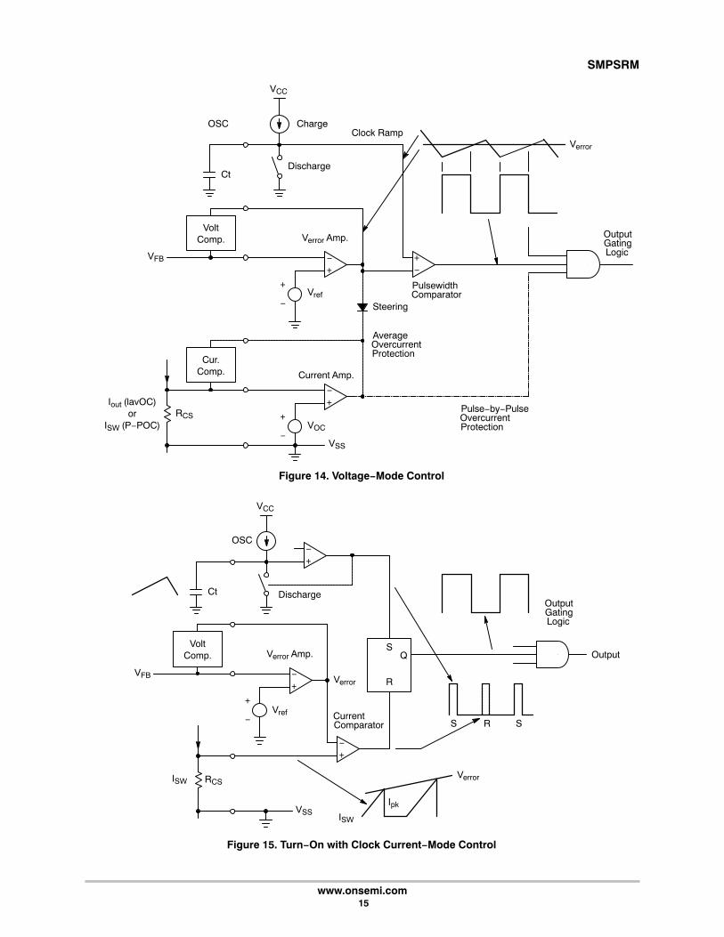
Voltage−mode control (see Figure 14) is typically usedfor forward−mode topologies. In voltage−mode control,only the output voltage is monitored. A voltage errorsignal is calculated by forming the difference betweenVout (actual) and Vout(desired). This error signal is thenfed into a comparator that compares it to the ramp voltagegenerated by the internal oscillator section of the controlIC. The comparator thus converts the voltage error signalinto the PWM drive signal to the power switch. Since theonly control parameter is the output voltage, and there isinherent delay through the power circuit, voltage−modecontrol tends to respond slowly to input variations.
Overcurrent protection for a voltage−mode controlledconverter can either be based on the average outputcurrent or use a pulse−by−pulse method. In averageovercurrent protection, the DC output current ismonitored, and if a threshold is exceeded, the pulse widthof the power switch is reduced. In pulse−by−pulseovercurrent protection, the peak current of each powerswitch “on” cycle is monitored and the power switch is
instantly cutoff if its limits are exceeded. This offersbetter protection to the power switch.
Current−mode control (see Figure 15) is typically usedwith boost−mode converters. Current−mode controlmonitors not only the output voltage, but also the outputcurrent. Here the voltage error signal is used to controlthe peak current within the magnetic elements duringeach power switch on−time. Current−mode control has avery rapid input and output response time, and has aninherent overcurrent protection. It is not commonly usedfor forward−mode converters; their current waveformshave much lower slopes in their current waveformswhich can create jitter within comparators.
Hysteretic control is a method of control which tries tokeep a monitored parameter between two limits. Thereare hysteretic current and voltage control methods, butthey are not commonly used.
The designer should be very careful when reviewing aprospective control IC data sheet. The method of controland any variations are usually not clearly described onthe first page of the data sheet.
SMPSRM
www.onsemi.com 15
−+
−+
+
−
−+
+
−
Cur.Comp.
VoltComp.
OSC ChargeClock Ramp
Discharge
Steering
AverageOvercurrentProtection
PulsewidthComparator
Pulse−by−PulseOvercurrentProtection
VCC
Verror
VSS
RCS
Verror Amp.
Ct
OutputGatingLogic
Vref
VOC
Iout (lavOC)or
ISW (P−POC)
Figure 14. Voltage−Mode Control
VFB
Current Amp.
−+
−+
+
−
VoltComp.
OSC
Discharge
VCC
VSS
RCS
Verror Amp.
CtOutputGatingLogic
Vref
ISW
Figure 15. Turn−On with Clock Current−Mode Control
−+
S
R
Q
S R S
Output
VFB
ISW
Ipk
Verror
CurrentComparator
Verror

SMPSRM
www.onsemi.com 16
The Choice of SemiconductorsPower Switches
The choice of which semiconductor technology to usefor the power switch function is influenced by manyfactors such as cost, peak voltage and current, frequencyof operation, and heatsinking. Each technology has itsown peculiarities that must be addressed during thedesign phase.
There are three major power switch choices: thebipolar junction transistor (BJT), the power MOSFET,and the integrated gate bipolar transistor (IGBT). TheBJT was the first power switch to be used in this field andstill offers many cost advantages over the others. It is alsostill used for very low cost or in high power switchingconverters. The maximum frequency of operation ofbipolar transistors is less than 80−100 kHz because ofsome of their switching characteristics. The IGBT is usedfor high power switching converters, displacing many ofthe BJT applications. They too, though, have a slowerswitching characteristic which limits their frequency ofoperation to below 30 kHz typically although some canreach 100 kHz. IGBTs have smaller die areas than powerMOSFETs of the same ratings, which typically means alower cost. Power MOSFETs are used in the majority ofapplications due to their ease of use and their higherfrequency capabilities. Each of the technologies will bereviewed.
The Bipolar Power TransistorThe BJT is a current driven device. That means that the
base current is in proportion to the current drawn throughthe collector. So one must provide:
IB � IC hFE (eq. 8)
In power transistors, the average gain (hFE) exhibited atthe higher collector currents is between 5 and 20. Thiscould create a large base drive loss if the base drive circuitis not properly designed.
One should generate a gate drive voltage that is as closeto 0.7 volts as possible. This is to minimize any losscreated by dropping the base drive voltage at the requiredbase current to the level exhibited by the base.
A second consideration is the storage time exhibited bythe collector during its turn−off transition. When the baseis overdriven, or where the base current is more thanneeded to sustain the collector current, the collectorexhibits a 0.3−2 �s delay in its turn−off which isproportional to the base overdrive. Although the storagetime is not a major source of loss, it does significantlylimit the maximum switching frequency of abipolar−based switching power supply. There are twomethods of reducing the storage time and increasing itsswitching time. The first is to use a base speed−upcapacitor whose value, typically around 100 pF, is placedin parallel with the base current limiting resistor(Figure 16a). The second is to use proportional base drive(Figure 16b). Here, only the amount of needed basecurrent is provided by the drive circuit by bleeding theexcess around the base into the collector.
The last consideration with BJTs is the risk ofexcessive second breakdown. This phenomenon iscaused by the resistance of the base across the die,permitting the furthest portions of the collector to turn offlater. This forces the current being forced through thecollector by an inductive load, to concentrate at theopposite ends of the die, thus causing an excessivelocalized heating on the die. This can result in ashort−circuit failure of the BJT which can happeninstantaneously if the amount of current crowding isgreat, or it can happen later if the amount of heating isless. Current crowding is always present when aninductive load is attached to the collector. By switchingthe BJT faster, with the circuits in Figure 15, one cangreatly reduce the effects of second breakdown on thereliability of the device.
VBB
VCE
+
−Control IC
VBE
+
−100 pF
Power Ground
VBB
Control IC Power Ground
100 pF
Figure 16. Driving a Bipolar Junction Transistor
(a) Fixed Base Drive Circuit (b) Proportional Base Drive Circuit (Baker Clamp)
SMPSRM
www.onsemi.com 17
The Power MOSFETPower MOSFETs are the popular choices used as
power switches and synchronous rectifiers. They are, onthe surface, simpler to use than BJTs, but they have somehidden complexities.
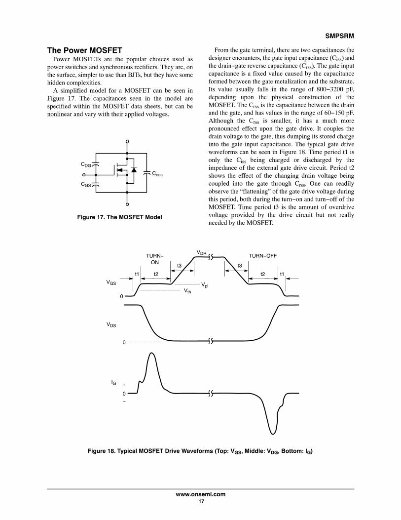
A simplified model for a MOSFET can be seen inFigure 17. The capacitances seen in the model arespecified within the MOSFET data sheets, but can benonlinear and vary with their applied voltages.
Coss
CDG
CGS
Figure 17. The MOSFET Model
From the gate terminal, there are two capacitances thedesigner encounters, the gate input capacitance (Ciss) andthe drain−gate reverse capacitance (Crss). The gate inputcapacitance is a fixed value caused by the capacitanceformed between the gate metalization and the substrate.Its value usually falls in the range of 800−3200 pF,depending upon the physical construction of theMOSFET. The Crss is the capacitance between the drainand the gate, and has values in the range of 60−150 pF.Although the Crss is smaller, it has a much morepronounced effect upon the gate drive. It couples thedrain voltage to the gate, thus dumping its stored chargeinto the gate input capacitance. The typical gate drivewaveforms can be seen in Figure 18. Time period t1 isonly the Ciss being charged or discharged by theimpedance of the external gate drive circuit. Period t2shows the effect of the changing drain voltage beingcoupled into the gate through Crss. One can readilyobserve the “flattening” of the gate drive voltage duringthis period, both during the turn−on and turn−off of theMOSFET. Time period t3 is the amount of overdrivevoltage provided by the drive circuit but not reallyneeded by the MOSFET.
Figure 18. Typical MOSFET Drive Waveforms (Top: VGS, Middle: VDG, Bottom: IG)
+
0
−
IG
0
VDS
VGS
0
TURN−ON
TURN−OFFVDR
Vth
Vpl
t3 t3
t2t1 t2 t1

SMPSRM
www.onsemi.com 18
The time needed to switch the MOSFET between onand off states is dependent upon the impedance of thegate drive circuit. It is very important that the drive circuitbe bypassed with a capacitor that will keep the drivevoltage constant over the drive period. A 0.1 �F capacitoris more than sufficient.
Driving MOSFETs in SwitchingPower Supply Applications
There are three things that are very important in thehigh frequency driving of MOSFETs: there must be atotem−pole driver; the drive voltage source must be wellbypassed; and the drive devices must be able to sourcehigh levels of current in very short periods of time (lowcompliance). The optimal drive circuit is shown inFigure 19.
Figure 19. Bipolar and FET−Based Drive Circuits (a. Bipolar Drivers, b. MOSFET Drivers)
LOADVG
Ron
a. Passive Turn−ON
LOADVG
Roff
b. Passive Turn−OFF
LOADVG
c. Bipolar Totem−pole
LOADVG
d. MOS Totem−pole
SMPSRM
www.onsemi.com 19
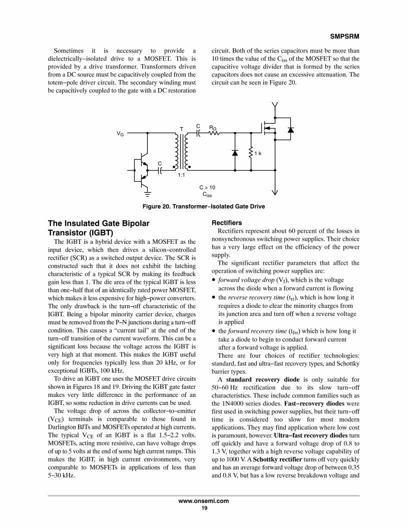
Sometimes it is necessary to provide adielectrically−isolated drive to a MOSFET. This isprovided by a drive transformer. Transformers drivenfrom a DC source must be capacitively coupled from thetotem−pole driver circuit. The secondary winding mustbe capacitively coupled to the gate with a DC restoration
circuit. Both of the series capacitors must be more than10 times the value of the Ciss of the MOSFET so that thecapacitive voltage divider that is formed by the seriescapacitors does not cause an excessive attenuation. Thecircuit can be seen in Figure 20.
VG
1 k
C RGT
C
C > 10Ciss
1:1
Figure 20. Transformer−Isolated Gate Drive
The Insulated Gate BipolarTransistor (IGBT)
The IGBT is a hybrid device with a MOSFET as theinput device, which then drives a silicon−controlledrectifier (SCR) as a switched output device. The SCR isconstructed such that it does not exhibit the latchingcharacteristic of a typical SCR by making its feedbackgain less than 1. The die area of the typical IGBT is lessthan one−half that of an identically rated power MOSFET,which makes it less expensive for high−power converters.The only drawback is the turn−off characteristic of theIGBT. Being a bipolar minority carrier device, chargesmust be removed from the P−N junctions during a turn−offcondition. This causes a “current tail” at the end of theturn−off transition of the current waveform. This can be asignificant loss because the voltage across the IGBT isvery high at that moment. This makes the IGBT usefulonly for frequencies typically less than 20 kHz, or forexceptional IGBTs, 100 kHz.
To drive an IGBT one uses the MOSFET drive circuitsshown in Figures 18 and 19. Driving the IGBT gate fastermakes very little difference in the performance of anIGBT, so some reduction in drive currents can be used.
The voltage drop of across the collector−to−emitter(VCE) terminals is comparable to those found inDarlington BJTs and MOSFETs operated at high currents.The typical VCE of an IGBT is a flat 1.5−2.2 volts.MOSFETs, acting more resistive, can have voltage dropsof up to 5 volts at the end of some high current ramps. Thismakes the IGBT, in high current environments, verycomparable to MOSFETs in applications of less than5−30 kHz.
RectifiersRectifiers represent about 60 percent of the losses in
nonsynchronous switching power supplies. Their choicehas a very large effect on the efficiency of the powersupply.
The significant rectifier parameters that affect theoperation of switching power supplies are:• forward voltage drop (Vf), which is the voltage
across the diode when a forward current is flowing• the reverse recovery time (trr), which is how long it
requires a diode to clear the minority charges fromits junction area and turn off when a reverse voltageis applied
• the forward recovery time (tfrr) which is how long ittake a diode to begin to conduct forward currentafter a forward voltage is applied.There are four choices of rectifier technologies:
standard, fast and ultra−fast recovery types, and Schottkybarrier types.
A standard recovery diode is only suitable for50−60 Hz rectification due to its slow turn−offcharacteristics. These include common families such asthe 1N4000 series diodes. Fast−recovery diodes werefirst used in switching power supplies, but their turn−offtime is considered too slow for most modernapplications. They may find application where low costis paramount, however. Ultra−fast recovery diodes turnoff quickly and have a forward voltage drop of 0.8 to1.3 V, together with a high reverse voltage capability ofup to 1000 V. A Schottky rectifier turns off very quicklyand has an average forward voltage drop of between 0.35and 0.8 V, but has a low reverse breakdown voltage and

SMPSRM
www.onsemi.com 20
a high reverse leakage current. For a typical switchingpower supply application, the best choice is usually aSchottky rectifier for output voltages less than 12 V, andan ultra−fast recovery diode for all other output voltages.
The major losses within output rectifiers areconduction losses and switching losses. The conductionloss is the forward voltage drop times the current flowingthrough it during its conduction period. This can besignificant if its voltage drop and current are high. Theswitching losses are determined by how fast a diode turnsoff (trr) times the reverse voltage across the rectifier. Thiscan be significant for high output voltages and currents.
The characteristics of power rectifiers and theirapplications in switching power supplies are covered ingreat detail in Reference (5).
The major losses within output rectifiers areconduction losses and switching losses. The conductionloss is the forward voltage drop times the current flowingthrough it during its conduction period. This can besignificant if its voltage drop and current are high. Theswitching losses are determined by how fast a diode turnsoff (trr) times the reverse voltage across the rectifier. Thiscan be significant for high output voltages and currents.
Table 2. Types of Rectifier Technologies
Rectifier Type Average Vf Reverse Recovery Time Typical Applications
Standard Recovery 0.7−1.0 V 1,000 ns 50−60 Hz Rectification
Fast Recovery 1.0−1.2 V 150−200 ns Output Rectification
UltraFast Recovery 0.9−1.4 V 25−75 nsOutput Rectification
(Vo > 12 V)
Schottky 0.3−0.8 V < 10 nsOutput Rectification
(Vo < 12 V)
Table 3. Estimating the Significant Parameters of the Power Semiconductors
TopologyBipolar Pwr Sw MOSFET Pwr Sw Rectifier
VCEO IC VDSS ID VR IF
Buck Vin Iout Vin Iout Vin Iout
Boost Vout(2.0 Pout)Vin(min)
Vout(2.0 Pout)Vin(min)
Vout Iout
Buck/Boost Vin � Vout2.0 Pout�
Vin(min) Vin � Vout(2.0 Pout)Vin(min)
Vin � Vout Iout
Flyback 1.7 Vin(max)(2.0 Pout)Vin(min)
1.5 Vin(max)(2.0 Pout)Vin(min)
5.0 Vout Iout
1 TransistorForward
2.0 Vin(1.5 Pout)Vin(min)
2.0 Vin(1.5 Pout)Vin(min)
3.0 Vout Iout
Push−Pull 2.0 Vin(1.2 Pout)Vin(min)
2.0 Vin(1.2 Pout)Vin(min)
2.0 Vout Iout
Half−Bridge Vin(2.0 Pout)Vin(min)
Vin(2.0 Pout)Vin(min)
2.0 Vout Iout
Full−Bridge Vin(1.2 Pout)Vin(min)
Vin(2.0 Pout)Vin(min)
2.0 Vout Iout

SMPSRM
www.onsemi.com 21
The Magnetic ComponentsThe magnetic elements within a switching power
supply are used either for stepping−up or down aswitched AC voltage, or for energy storage. Inforward−mode topologies, the transformer is only usedfor stepping−up or down the AC voltage generated by thepower switches. The output filter (the output inductorand capacitor) in forward−mode topologies is used forenergy storage. In boost−mode topologies, thetransformer is used both for energy storage and to providea step−up or step−down function.
Many design engineers consider the magneticelements of switching power supplies counter−intuitiveor too complicated to design. Fortunately, help is at hand;the suppliers of magnetic components have applicationsengineers who are quite capable of performing thetransformer design and discussing the tradeoffs neededfor success. For those who are more experienced or moreadventuresome, please refer to Reference 2 in theBibliography for transformer design guidelines.
The general procedure in the design of any magneticcomponent is as follows (Reference 2, p 42):
1. Select an appropriate core material for theapplication and the frequency of operation.
2. Select a core form factor that is appropriate forthe application and that satisfies applicableregulatory requirements.
3. Determine the core cross−sectional areanecessary to handle the required power
4. Determine whether an airgap is needed andcalculate the number of turns needed for eachwinding. Then determine whether the accuracyof the output voltages meets the requirementsand whether the windings will fit into theselected core size.
5. Wind the magnetic component using properwinding techniques.
6. During the prototype stage, verify thecomponent’s operation with respect to the levelof voltage spikes, cross−regulation, outputaccuracy and ripple, RFI, etc., and makecorrections were necessary.
The design of any magnetic component is a “calculatedestimate.” There are methods of “stretching” the designlimits for smaller size or lower losses, but these tend tobe diametrically opposed to one another. One should becautious when doing this.
Some useful sources for magnetics components are:
CoilCraft, Inc.website: www.coilcraft.com/email: [email protected]: 847−639−6400
Coiltronics, Division of Cooper ElectronicsTechnology
website: www.coiltronics.comTelephone: 561−241−7876
Cramer Coil, Inc.website: www.cramerco.comemail: [email protected]: 262−268−2150
Pulse, Inc.website: www.pulseeng.comTelephone: 858−674−8100
TDKwebsite: www.component.talk.comTelephone: 847−803−6100
Würth Elektronikwebsite: www.we−online.comemail: cbt@we−online.comTelephone: +49 7940 946−0
Laying Out the Printed Circuit BoardThe printed circuit board (PCB) layout is the third
critical portion of every switching power supply designin addition to the basic design and the magnetics design.Improper layout can adversely affect RFI radiation,component reliability, efficiency and stability. EveryPCB layout will be different, but if the designerappreciates the common factors present in all switchingpower supplies, the process will be simplified.
All PCB traces exhibit inductance and resistance.These can cause high voltage transitions whenever thereis a high rate of change in current flowing through thetrace. For operational amplifiers sharing a trace withpower signals, it means that the supply would beimpossible to stabilize. For traces that are too narrow forthe current flowing through them, it means a voltage dropfrom one end of the trace to the other which potentiallycan be an antenna for RFI. In addition, capacitivecoupling between adjacent traces can interfere withproper circuit operation.
There are two rules of thumb for PCB layouts: “shortand fat” for all power−carrying traces and “one pointgrounding” for the various ground systems within aswitching power supply. Traces that are short and fatminimize the inductive and resistive aspects of the trace,thus reducing noise within the circuits and RFI.Single−point grounding keeps the noise sourcesseparated from the sensitive control circuits.
SMPSRM
www.onsemi.com 22
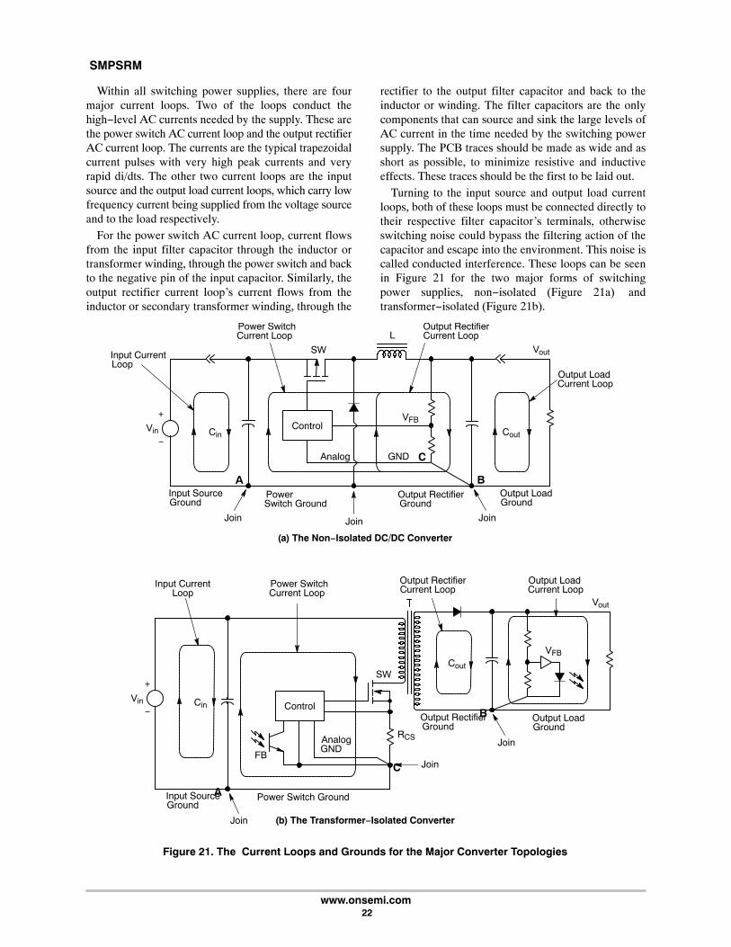
Within all switching power supplies, there are fourmajor current loops. Two of the loops conduct thehigh−level AC currents needed by the supply. These arethe power switch AC current loop and the output rectifierAC current loop. The currents are the typical trapezoidalcurrent pulses with very high peak currents and veryrapid di/dts. The other two current loops are the inputsource and the output load current loops, which carry lowfrequency current being supplied from the voltage sourceand to the load respectively.
For the power switch AC current loop, current flowsfrom the input filter capacitor through the inductor ortransformer winding, through the power switch and backto the negative pin of the input capacitor. Similarly, theoutput rectifier current loop’s current flows from theinductor or secondary transformer winding, through the
rectifier to the output filter capacitor and back to theinductor or winding. The filter capacitors are the onlycomponents that can source and sink the large levels ofAC current in the time needed by the switching powersupply. The PCB traces should be made as wide and asshort as possible, to minimize resistive and inductiveeffects. These traces should be the first to be laid out.
Turning to the input source and output load currentloops, both of these loops must be connected directly totheir respective filter capacitor’s terminals, otherwiseswitching noise could bypass the filtering action of thecapacitor and escape into the environment. This noise iscalled conducted interference. These loops can be seenin Figure 21 for the two major forms of switchingpower supplies, non−isolated (Figure 21a) andtransformer−isolated (Figure 21b).
+
−Cin Cout
Figure 21. The Current Loops and Grounds for the Major Converter Topologies
Vin
L
Control
Input CurrentLoop
Join Join
Power SwitchCurrent Loop
Join
GNDAnalog
SW
Output LoadCurrent Loop
Output LoadGround
Output RectifierGround
PowerSwitch Ground
Input SourceGround
Vout
VFB
Output RectifierCurrent Loop
Cin
Cout
VinControl
Input CurrentLoop
Join
Join
Power SwitchCurrent Loop
JoinAnalog
SW
Output LoadCurrent Loop
Output LoadGround
Output RectifierGround
Input SourceGround
Vout
VFB
Output RectifierCurrent Loop
GND
Power Switch Ground
FB
RCS
(a) The Non−Isolated DC/DC Converter
(b) The Transformer−Isolated Converter
+
−
A B
C
A
B
C

SMPSRM
www.onsemi.com 23
The grounds are extremely important to the properoperation of the switching power supply, since they formthe reference connections for the entire supply; eachground has its own unique set of signals which canadversely affect the operation of the supply if connectedimproperly.
There are five distinct grounds within the typicalswitching power supply. Four of them form the returnpaths for the current loops described above. Theremaining ground is the low−level analog control groundwhich is critical for the proper operation of the supply.The grounds which are part of the major current loopsmust be connected together exactly as shown inFigure 21. Here again, the connecting point between thehigh−level AC grounds and the input or output groundsis at the negative terminal of the appropriate filtercapacitor (points A and B in Figures 21a and 21b). Noiseon the AC grounds can very easily escape into theenvironment if the grounds are not directly connected tothe negative terminal of the filter capacitor(s). Theanalog control ground must be connected to the pointwhere the control IC and associated circuitry mustmeasure key power parameters, such as AC or DCcurrent and the output voltage (point C in Figures 21a and21b). Here any noise introduced by large AC signalswithin the AC grounds will sum directly onto thelow−level control parameters and greatly affect theoperation of the supply. The purpose of connecting thecontrol ground to the lower side of the current sensingresistor or the output voltage resistor divider is to form a“Kelvin contact” where any common mode noise is notsensed by the control circuit. In short, follow the examplegiven by Figure 21 exactly as shown for best results.
The last important factor in the PCB design is thelayout surrounding the AC voltage nodes. These are thedrain of the power MOSFET (or collector of a BJT) andthe anode of the output rectifier(s). These nodes cancapacitively couple into any trace on different layers ofthe PCB that run underneath the AC pad. In surfacemount designs, these nodes also need to be large enoughto provide heatsinking for the power switch or rectifier.This is at odds with the desire to keep the pad as small aspossible to discourage capacitive coupling to othertraces. One good compromise is to make all layers belowthe AC node identical to the AC node and connect themwith many vias (plated−through holes). This greatlyincreases the thermal mass of the pad for improvedheatsinking and locates any surrounding traces offlaterally where the coupling capacitance is much smaller.An example of this can be seen in Figure 22.
Many times it is necessary to parallel filter capacitorsto reduce the amount of RMS ripple current eachcapacitor experiences. Close attention should be paid tothis layout. If the paralleled capacitors are in a line, thecapacitor closest to the source of the ripple current willoperate hotter than the others, shortening its operatinglife; the others will not see this level of AC current. Toensure that they will evenly share the ripple current,ideally, any paralleled capacitors should be laid out in aradially−symmetric manner around the current source,typically a rectifier or power switch.
The PCB layout, if not done properly, can ruin a goodpaper design. It is important to follow these basicguidelines and monitor the layout every step of theprocess.
ÉÉÉÉ
ÉÉÉÉ
ÉÉÉÉ
ÉÉÉÉÂÂÂÂÂÂÂÂÂÂÂÂÂÂÂÂÂÂÂÂÂÂ
Power Device
Via PCB Top
PCB BottomPlated−Thru Hole
Figure 22. Method for Minimizing AC Capacitive Coupling and Enhancing Heatsinking
SMPSRM
www.onsemi.com 24
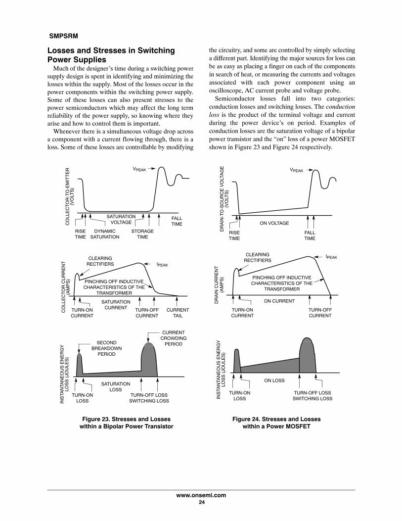
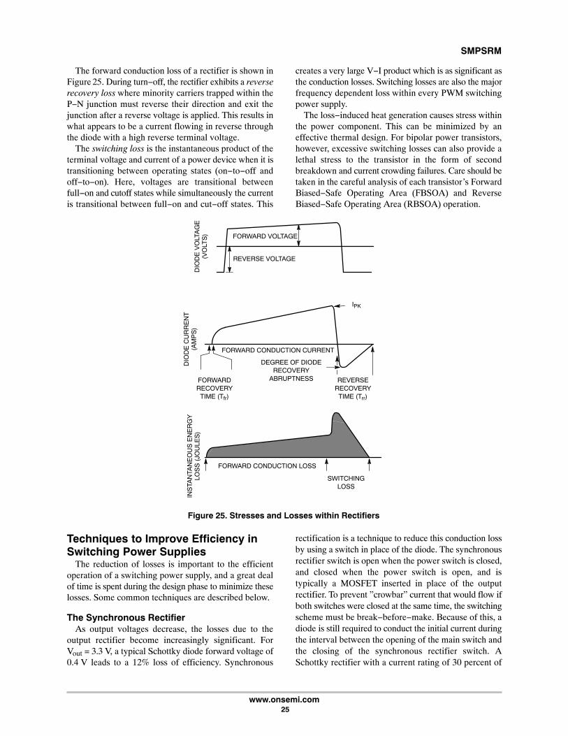
Losses and Stresses in SwitchingPower Supplies
Much of the designer’s time during a switching powersupply design is spent in identifying and minimizing thelosses within the supply. Most of the losses occur in thepower components within the switching power supply.Some of these losses can also present stresses to thepower semiconductors which may affect the long termreliability of the power supply, so knowing where theyarise and how to control them is important.
Whenever there is a simultaneous voltage drop acrossa component with a current flowing through, there is aloss. Some of these losses are controllable by modifying
the circuitry, and some are controlled by simply selectinga different part. Identifying the major sources for loss canbe as easy as placing a finger on each of the componentsin search of heat, or measuring the currents and voltagesassociated with each power component using anoscilloscope, AC current probe and voltage probe.
Semiconductor losses fall into two categories:conduction losses and switching losses. The conductionloss is the product of the terminal voltage and currentduring the power device’s on period. Examples ofconduction losses are the saturation voltage of a bipolarpower transistor and the “on” loss of a power MOSFETshown in Figure 23 and Figure 24 respectively.
TURN-ONCURRENT
CURRENTTAIL
TURN-OFFCURRENT
SATURATIONCURRENT
PINCHING OFF INDUCTIVECHARACTERISTICS OF THE
TRANSFORMER
IPEAK
CO
LLE
CTO
R C
UR
RE
NT
(AM
PS
)
FALLTIME
STORAGETIME
DYNAMICSATURATION
RISETIME
SATURATIONVOLTAGE
VPEAK
CO
LLE
CTO
R-T
O-E
MIT
TE
R(V
OLT
S)
Figure 23. Stresses and Losseswithin a Bipolar Power Transistor
SATURATIONLOSS
TURN-ONLOSS
TURN-OFF LOSSSWITCHING LOSSIN
STA
NTA
NE
OU
S E
NE
RG
YLO
SS
(JO
ULE
S)
CURRENTCROWDING
PERIODSECONDBREAKDOWN
PERIOD
DR
AIN
-TO
-SO
UR
CE
VO
LTA
GE
(VO
LTS
)
DR
AIN
CU
RR
EN
T(A
MP
S)
Figure 24. Stresses and Losseswithin a Power MOSFET
INS
TAN
TAN
EO
US
EN
ER
GY
LOS
S (
JOU
LES
)
FALLTIME
RISETIME
ON VOLTAGE
VPEAK
TURN-ONCURRENT
TURN-OFFCURRENT
ON CURRENT
PINCHING OFF INDUCTIVECHARACTERISTICS OF THE
TRANSFORMER
IPEAKCLEARING
RECTIFIERS
ON LOSS
TURN-ONLOSS
TURN-OFF LOSSSWITCHING LOSS
CLEARINGRECTIFIERS
SMPSRM
www.onsemi.com 25
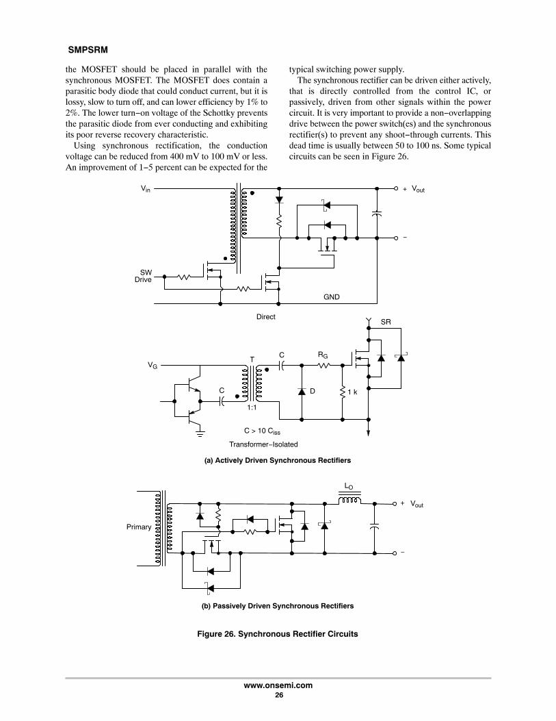
The forward conduction loss of a rectifier is shown inFigure 25. During turn−off, the rectifier exhibits a reverserecovery loss where minority carriers trapped within theP−N junction must reverse their direction and exit thejunction after a reverse voltage is applied. This results inwhat appears to be a current flowing in reverse throughthe diode with a high reverse terminal voltage.
The switching loss is the instantaneous product of theterminal voltage and current of a power device when it istransitioning between operating states (on−to−off andoff−to−on). Here, voltages are transitional betweenfull−on and cutoff states while simultaneously the currentis transitional between full−on and cut−off states. This
creates a very large V−I product which is as significant asthe conduction losses. Switching losses are also the majorfrequency dependent loss within every PWM switchingpower supply.
The loss−induced heat generation causes stress withinthe power component. This can be minimized by aneffective thermal design. For bipolar power transistors,however, excessive switching losses can also provide alethal stress to the transistor in the form of secondbreakdown and current crowding failures. Care should betaken in the careful analysis of each transistor’s ForwardBiased−Safe Operating Area (FBSOA) and ReverseBiased−Safe Operating Area (RBSOA) operation.
Figure 25. Stresses and Losses within Rectifiers
REVERSE VOLTAGE
FORWARD VOLTAGE
DIO
DE
VO
LTA
GE
(VO
LTS
)
DEGREE OF DIODERECOVERY
ABRUPTNESS REVERSERECOVERY
TIME (Trr)
FORWARD CONDUCTION CURRENT
FORWARDRECOVERY
TIME (Tfr)
IPK
DIO
DE
CU
RR
EN
T(A
MP
S)
SWITCHINGLOSS
FORWARD CONDUCTION LOSS
INS
TAN
TAN
EO
US
EN
ER
GY
LOS
S (
JOU
LES
)
Techniques to Improve Efficiency inSwitching Power Supplies
The reduction of losses is important to the efficientoperation of a switching power supply, and a great dealof time is spent during the design phase to minimize theselosses. Some common techniques are described below.
The Synchronous RectifierAs output voltages decrease, the losses due to the
output rectifier become increasingly significant. ForVout = 3.3 V, a typical Schottky diode forward voltage of0.4 V leads to a 12% loss of efficiency. Synchronous
rectification is a technique to reduce this conduction lossby using a switch in place of the diode. The synchronousrectifier switch is open when the power switch is closed,and closed when the power switch is open, and istypically a MOSFET inserted in place of the outputrectifier. To prevent ”crowbar” current that would flow ifboth switches were closed at the same time, the switchingscheme must be break−before−make. Because of this, adiode is still required to conduct the initial current duringthe interval between the opening of the main switch andthe closing of the synchronous rectifier switch. ASchottky rectifier with a current rating of 30 percent of
SMPSRM
www.onsemi.com 26
the MOSFET should be placed in parallel with thesynchronous MOSFET. The MOSFET does contain aparasitic body diode that could conduct current, but it islossy, slow to turn off, and can lower efficiency by 1% to2%. The lower turn−on voltage of the Schottky preventsthe parasitic diode from ever conducting and exhibitingits poor reverse recovery characteristic.
Using synchronous rectification, the conductionvoltage can be reduced from 400 mV to 100 mV or less.An improvement of 1−5 percent can be expected for the
typical switching power supply.The synchronous rectifier can be driven either actively,
that is directly controlled from the control IC, orpassively, driven from other signals within the powercircuit. It is very important to provide a non−overlappingdrive between the power switch(es) and the synchronousrectifier(s) to prevent any shoot−through currents. Thisdead time is usually between 50 to 100 ns. Some typicalcircuits can be seen in Figure 26.
LO
+
−
Vout
+
−
VoutVin
SWDrive
GND
Direct
DC
RGC
1:1
C > 10 Ciss
SR
Primary
VG
1 k
Figure 26. Synchronous Rectifier Circuits
(b) Passively Driven Synchronous Rectifiers
(a) Actively Driven Synchronous Rectifiers
Transformer−Isolated
SMPSRM
www.onsemi.com 27
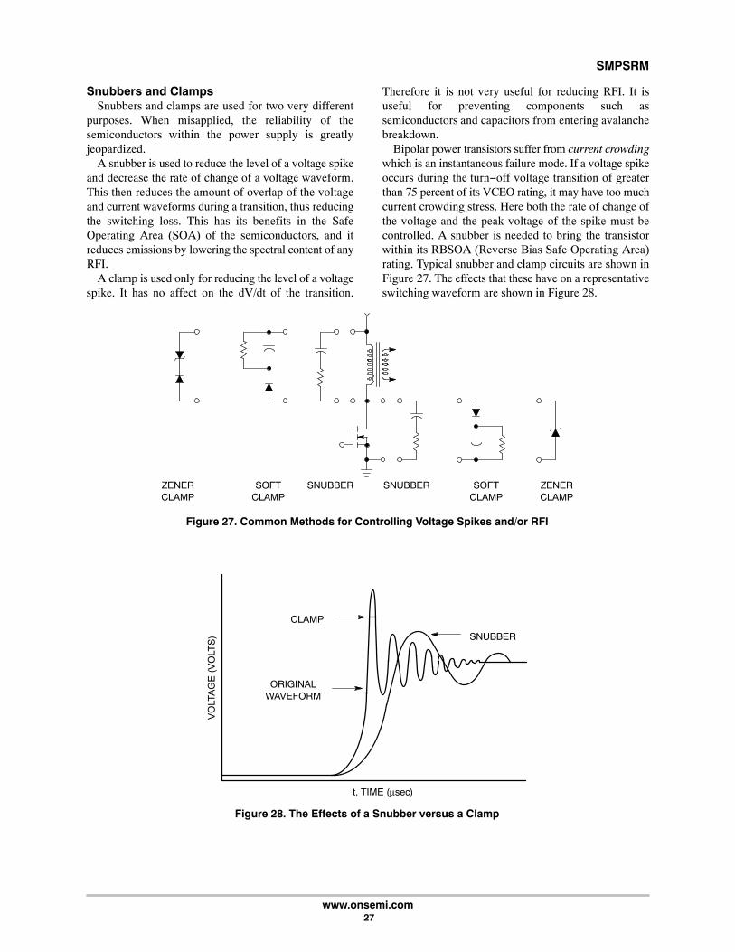
Snubbers and ClampsSnubbers and clamps are used for two very different
purposes. When misapplied, the reliability of thesemiconductors within the power supply is greatlyjeopardized.
A snubber is used to reduce the level of a voltage spikeand decrease the rate of change of a voltage waveform.This then reduces the amount of overlap of the voltageand current waveforms during a transition, thus reducingthe switching loss. This has its benefits in the SafeOperating Area (SOA) of the semiconductors, and itreduces emissions by lowering the spectral content of anyRFI.
A clamp is used only for reducing the level of a voltagespike. It has no affect on the dV/dt of the transition.
Therefore it is not very useful for reducing RFI. It isuseful for preventing components such assemiconductors and capacitors from entering avalanchebreakdown.
Bipolar power transistors suffer from current crowdingwhich is an instantaneous failure mode. If a voltage spikeoccurs during the turn−off voltage transition of greaterthan 75 percent of its VCEO rating, it may have too muchcurrent crowding stress. Here both the rate of change ofthe voltage and the peak voltage of the spike must becontrolled. A snubber is needed to bring the transistorwithin its RBSOA (Reverse Bias Safe Operating Area)rating. Typical snubber and clamp circuits are shown inFigure 27. The effects that these have on a representativeswitching waveform are shown in Figure 28.
Figure 27. Common Methods for Controlling Voltage Spikes and/or RFI
ZENERCLAMP
SOFTCLAMP
SNUBBERSNUBBERSOFTCLAMP
ZENERCLAMP
Figure 28. The Effects of a Snubber versus a Clamp
SNUBBER
CLAMP
ORIGINALWAVEFORM
VO
LTA
GE
(V
OLT
S)
t, TIME (μsec)
SMPSRM
www.onsemi.com 28
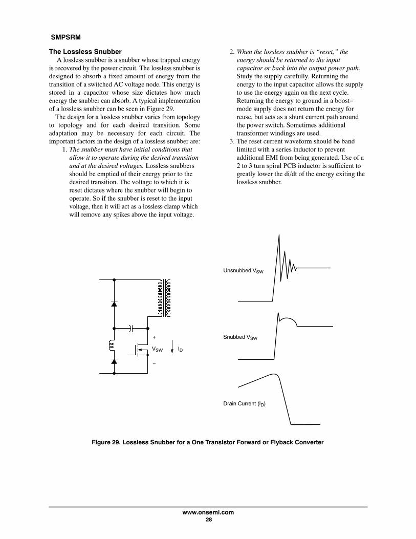
The Lossless Snubber A lossless snubber is a snubber whose trapped energy
is recovered by the power circuit. The lossless snubber isdesigned to absorb a fixed amount of energy from thetransition of a switched AC voltage node. This energy isstored in a capacitor whose size dictates how muchenergy the snubber can absorb. A typical implementationof a lossless snubber can be seen in Figure 29.
The design for a lossless snubber varies from topologyto topology and for each desired transition. Someadaptation may be necessary for each circuit. Theimportant factors in the design of a lossless snubber are:
1. The snubber must have initial conditions thatallow it to operate during the desired transitionand at the desired voltages. Lossless snubbersshould be emptied of their energy prior to thedesired transition. The voltage to which it isreset dictates where the snubber will begin tooperate. So if the snubber is reset to the inputvoltage, then it will act as a lossless clamp whichwill remove any spikes above the input voltage.
2. When the lossless snubber is “reset,” theenergy should be returned to the inputcapacitor or back into the output power path.Study the supply carefully. Returning theenergy to the input capacitor allows the supplyto use the energy again on the next cycle.Returning the energy to ground in a boost−mode supply does not return the energy forreuse, but acts as a shunt current path aroundthe power switch. Sometimes additionaltransformer windings are used.
3. The reset current waveform should be bandlimited with a series inductor to preventadditional EMI from being generated. Use of a2 to 3 turn spiral PCB inductor is sufficient togreatly lower the di/dt of the energy exiting thelossless snubber.
+
−
VSW ID
Unsnubbed VSW
Snubbed VSW
Drain Current (ID)
Figure 29. Lossless Snubber for a One Transistor Forward or Flyback Converter
SMPSRM
www.onsemi.com 29
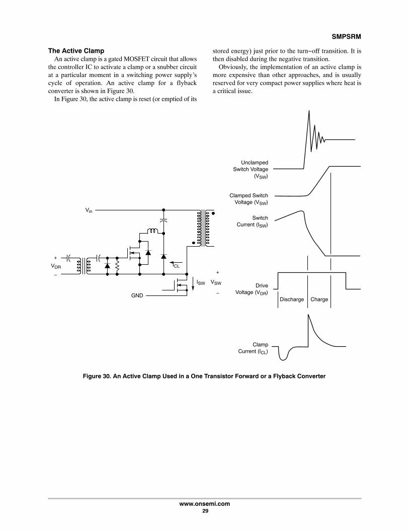
The Active ClampAn active clamp is a gated MOSFET circuit that allows
the controller IC to activate a clamp or a snubber circuitat a particular moment in a switching power supply’scycle of operation. An active clamp for a flybackconverter is shown in Figure 30.
In Figure 30, the active clamp is reset (or emptied of its
stored energy) just prior to the turn−off transition. It isthen disabled during the negative transition.
Obviously, the implementation of an active clamp ismore expensive than other approaches, and is usuallyreserved for very compact power supplies where heat isa critical issue.
GND
+
−
ISW VSW
VDR
+
−
ICL
UnclampedSwitch Voltage
(VSW)
Clamped SwitchVoltage (VSW)
SwitchCurrent (ISW)
DriveVoltage (VDR)
ClampCurrent (ICL)
Discharge Charge
Vin
Figure 30. An Active Clamp Used in a One Transistor Forward or a Flyback Converter

SMPSRM
www.onsemi.com 30
Quasi−Resonant TopologiesA quasi−resonant topology is designed to reduce or
eliminate the frequency−dependent switching losseswithin the power switches and rectifiers. Switchinglosses account for about 40% of the total loss within aPWM power supply and are proportional to the switchingfrequency. Eliminating these losses allows the designerto increase the operating frequency of the switchingpower supply and so use smaller inductors andcapacitors, reducing size and weight. In addition, RFIlevels are reduced due to the controlled rate of change ofcurrent or voltage.
The downside to quasi−resonant designs is that theyare more complex than non−resonant topologies due toparasitic RF effects that must be considered when
switching frequencies are in the 100’s of kHz.Schematically, quasi−resonant topologies are minor
modifications of the standard PWM topologies. Aresonant tank circuit is added to the power switch sectionto make either the current or the voltage “ring” througha half a sinusoid waveform. Since the sinusoid starts atzero and ends at zero, the product of the voltage andcurrent at the starting and ending points is zero, thus hasno switching loss.
There are two quasi−resonant methods: zero currentswitching (ZCS) or zero voltage switching (ZVS). ZCSis a fixed on−time, variable off−time method of control.ZCS starts from an initial condition where the powerswitch is off and no current is flowing through theresonant inductor. The ZCS quasi−resonant buckconverter is shown in Figure 31.
Figure 31. Schematic and Waveforms for a ZCS Quasi-Resonant Buck Converter
VinCin
CRVSW
FEEDBACK
VoutCout
LO
ILR
CONTROL
Vin
POWER SWITCHON
SWITCHTURN-OFF
VS
WI
LRV
D
LR
A ZCS Quasi−Resonant Buck Converter
IPK
D

SMPSRM
www.onsemi.com 31
In this design, both the power switch and the catchdiode operate in a zero current switching mode. Power ispassed to the output during the resonant periods. So toincrease the power delivered to the load, the frequencywould increase, and vice versa for decreasing loads. Intypical designs the frequency can change 10:1 over theZCS supply’s operating range.
The ZVS is a fixed off−time, variable on−time methodcontrol. Here the initial condition occurs when the powerswitch is on, and the familiar current ramp is flowingthrough the filter inductor. The ZVS quasi−resonant buckconverter is shown in Figure 32. Here, to control the
power delivered to the load, the amount of “resonant offtimes” are varied. For light loads, the frequency is high.When the load is heavy, the frequency drops. In a typicalZVS power supply, the frequency typically varies 4:1over the entire operating range of the supply.
There are other variations on the resonant theme thatpromote zero switching losses, such as full resonantPWM, full and half−bridge topologies for higher powerand resonant transition topologies. For a more detailedtreatment, see Chapter 4 in the “Power SupplyCookbook” (Bibliography reference 3).
LOLR
Figure 32. Schematic and Waveforms for aZVS Quasi-Resonant Buck Converter
CRVoutCoutFEEDBACK
DVI/P
CONTROLCin
Vin
ILOAD
IPK
0
I SW
I D
A ZVS Quasi−Resonant Buck Converter
Vin � VoutLR � LO
VinLR
0
POWER SWITCHTURNS ON
Vin
VI/P
SMPSRM
www.onsemi.com 32
Power Factor CorrectionPower Factor (PF) is defined as the ratio of real power
to apparent power. In a typical AC power supplyapplication where both the voltage and current aresinusoidal, the PF is given by the cosine of the phaseangle between the input current and the input voltage andis a measure of how much of the current contributes toreal power in the load. A power factor of unity indicatesthat 100% of the current is contributing to power in theload while a power factor of zero indicates that none ofthe current contributes to power in the load. Purelyresistive loads have a power factor of unity; the currentthrough them is directly proportional to the appliedvoltage.
The current in an ac line can be thought of as consistingof two components: real and imaginary. The real partresults in power absorbed by the load while the imaginarypart is power being reflected back into the source, suchas is the case when current and voltage are of oppositepolarity and their product, power, is negative.
It is important to have a power factor as close aspossible to unity so that none of the delivered power isreflected back to the source. Reflected power isundesirable for three reasons:
1. The transmission lines or power cord willgenerate heat according to the total currentbeing carried, the real part plus the reflectedpart. This causes problems for the electricutilities and has prompted various regulations
requiring all electrical equipment connected toa low voltage distribution system to minimizecurrent harmonics and maximize power factor.
2. The reflected power not wasted in theresistance of the power cord may generateunnecessary heat in the source (the localstep−down transformer), contributing topremature failure and constituting a fire hazard.
3. Since the ac mains are limited to a finite currentby their circuit breakers, it is desirable to getthe most power possible from the given currentavailable. This can only happen when thepower factor is close to or equal to unity.
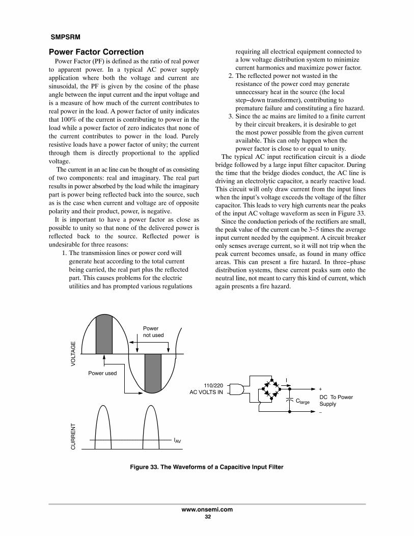
The typical AC input rectification circuit is a diodebridge followed by a large input filter capacitor. Duringthe time that the bridge diodes conduct, the AC line isdriving an electrolytic capacitor, a nearly reactive load.This circuit will only draw current from the input lineswhen the input’s voltage exceeds the voltage of the filtercapacitor. This leads to very high currents near the peaksof the input AC voltage waveform as seen in Figure 33.
Since the conduction periods of the rectifiers are small,the peak value of the current can be 3−5 times the averageinput current needed by the equipment. A circuit breakeronly senses average current, so it will not trip when thepeak current becomes unsafe, as found in many officeareas. This can present a fire hazard. In three−phasedistribution systems, these current peaks sum onto theneutral line, not meant to carry this kind of current, whichagain presents a fire hazard.
Figure 33. The Waveforms of a Capacitive Input Filter
Clarge
110/220AC VOLTS IN
DC To PowerSupply
IPower used
Powernot used
VO
LTA
GE
CU
RR
EN
T
IAV
+
−
SMPSRM
www.onsemi.com 33
A Power Factor Correction (PFC) circuit is a switchingpower converter, essentially a boost converter with a verywide input range, that precisely controls its input currenton an instantaneous basis to match the waveshape andphase of the input voltage. This represents a zero degreesor 100 percent power factor and mimics a purely resistiveload. The amplitude of the input current waveform isvaried over longer time frames to maintain a constantvoltage at the converter’s output filter capacitor. Thismimics a resistor which slowly changes value to absorbthe correct amount of power to meet the demand of theload. Short term energy excesses and deficits caused bysudden changes in the load are supplemented by a ”bulkenergy storage capacitor”, the boost converter’s outputfilter device. The PFC input filter capacitor is reduced toa few microfarads, thus placing a half−wave haversinewaveshape into the PFC converter.
The PFC boost converter can operate down to about30 V before there is insufficient voltage to draw any moresignificant power from its input. The converter then canbegin again when the input haversine reaches 30 V on thenext half−wave haversine. This greatly increases theconduction angle of the input rectifiers. The drop−outregion of the PFC converter is then filtered (smoothed)by the input EMI filter.
A PFC circuit not only ensures that no power isreflected back to the source, it also eliminates thehigh current pulses associated with conventionalrectifier−filter input circuits. Because heat lost in thetransmission line and adjacent circuits is proportional tothe square of the current in the line, short strong current
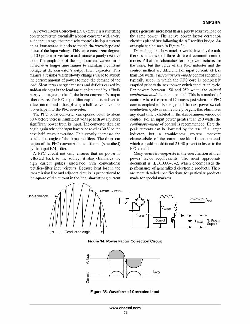
pulses generate more heat than a purely resistive load ofthe same power. The active power factor correctioncircuit is placed just following the AC rectifier bridge. Anexample can be seen in Figure 34.
Depending upon how much power is drawn by the unit,there is a choice of three different common controlmodes. All of the schematics for the power sections arethe same, but the value of the PFC inductor and thecontrol method are different. For input currents of lessthan 150 watts, a discontinuous−mode control scheme istypically used, in which the PFC core is completelyemptied prior to the next power switch conduction cycle.For powers between 150 and 250 watts, the criticalconduction mode is recommended. This is a method ofcontrol where the control IC senses just when the PFCcore is emptied of its energy and the next power switchconduction cycle is immediately begun; this eliminatesany dead time exhibited in the discontinuous−mode ofcontrol. For an input power greater than 250 watts, thecontinuous−mode of control is recommended. Here thepeak currents can be lowered by the use of a largerinductor, but a troublesome reverse recoverycharacteristic of the output rectifier is encountered,which can add an additional 20−40 percent in losses to thePFC circuit.
Many countries cooperate in the coordination of theirpower factor requirements. The most appropriatedocument is IEC61000−3−2, which encompasses theperformance of generalized electronic products. Thereare more detailed specifications for particular productsmade for special markets.
Input Voltage
Switch Current
Conduction Angle
Figure 34. Power Factor Correction Circuit
ClargeControl
Csmall
I
Vsense
Vout
To PowerSupply
+
−
Figure 35. Waveform of Corrected Input
Vol
tage
Cur
rent
IAVG

SMPSRM
www.onsemi.com 34
Bibliography
1. ON Semiconductor, Power Factor Correction (PFC) Handbook, HBD853/D, 2012.2. Ben−Yaakov Sam, Gregory Ivensky, “Passive Lossless Snubbers for High Frequency PWM Converters,”
Seminar 12, APEC 99.3. Brown, Marty, Power Supply Cookbook, Butterworth−Heinemann, 1994, 2001.4. Brown, Marty, “Laying Out PC Boards for Embedded Switching Supplies,” Electronic Design, Dec. 1999.5. Martin, Robert F., “Harmonic Currents,” Compliance Engineering − 1999 Annual Resources Guide, Cannon
Communications, LLC, pp. 103−107.6. Christophe Basso, Switch−Mode Power Supplies, SPICE Simulations and Practical Designs, McGraw−Hill,
2008, ISBN 978−0−07−150859−9.7. Christophe Basso, Designing Control Loops for Linear and Switching Power Supplies: A Tutorial Guide,
Artech House, 2012, ISBN 978−1−60807−557−7.

SMPSRM
www.onsemi.com 35
Topology Overview

SMPSRM
www.onsemi.com 36

SMPSRM
www.onsemi.com 37

SMPSRM
www.onsemi.com 38

SMPSRM
www.onsemi.com 39

SMPSRM
www.onsemi.com 40

SMPSRM
www.onsemi.com 41

SMPSRM
www.onsemi.com 42

SMPSRM
www.onsemi.com 43

SMPSRM
www.onsemi.com 44

SMPSRM
www.onsemi.com 45

SMPSRM
www.onsemi.com 46
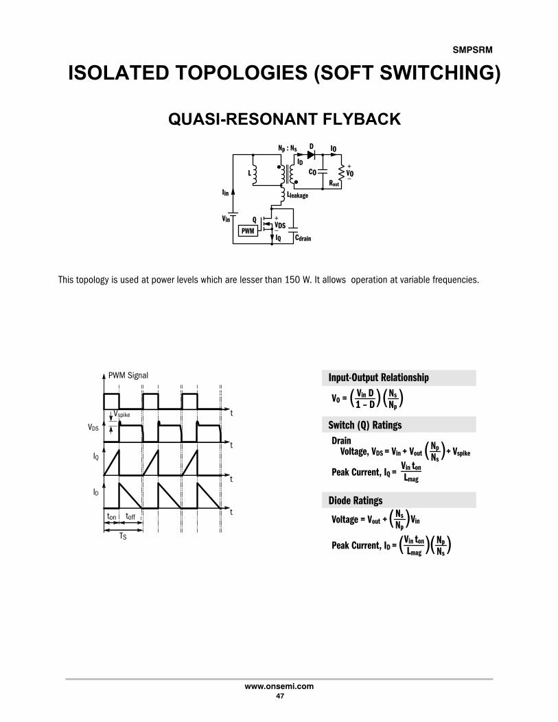
SMPSRM
www.onsemi.com 47

SMPSRM
www.onsemi.com 48
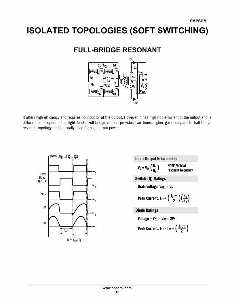
SMPSRM
www.onsemi.com 49
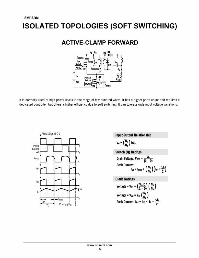
SMPSRM
www.onsemi.com 50

SMPSRM
www.onsemi.com 51
Switch−Mode Power Supply ExamplesThis section provides both initial and detailed information to simplify the selection and design of a variety of
Switch−Mode power supplies. The ICs for Switching Power Supplies figure identifies control, reference voltage, outputprotection and switching regulator ICs for various topologies.
Page
ICs for Switching Power Supplies 52. . . . . . . . . . . . . . . . . . . . . . . . . . . . . . . . . . . . . . . . . . . . . . . . . . . . . . . . . . . . . . .Integrated circuits identified for various sections of a switching power supply.
Real SMPS ApplicationsUp to 25 W Flyback Switch−Mode Power Supply 53. . . . . . . . . . . . . . . . . . . . . . . . . . . . . . . . . . . . . . . . . . . . . . . .25 to 150 W Flyback Switch−Mode Power Supply 54. . . . . . . . . . . . . . . . . . . . . . . . . . . . . . . . . . . . . . . . . . . . . . .150 to 500 W Resonant Switch−Mode Power Supply 56. . . . . . . . . . . . . . . . . . . . . . . . . . . . . . . . . . . . . . . . . . . . .100 W Boost CRM PFC 57. . . . . . . . . . . . . . . . . . . . . . . . . . . . . . . . . . . . . . . . . . . . . . . . . . . . . . . . . . . . . . . . . . . .120 W High Efficiency, High Voltage, Active X2, <30 mW No Load PFC 58. . . . . . . . . . . . . . . . . . . . . . . . . . . .300 W Compact Continuous Conduction Mode PFC 59. . . . . . . . . . . . . . . . . . . . . . . . . . . . . . . . . . . . . . . . . . . . . .Up to 15 W AC−DC Compact Power Supply 60. . . . . . . . . . . . . . . . . . . . . . . . . . . . . . . . . . . . . . . . . . . . . . . . . . . .25 W Offline Power Supply High Voltage Switcher 61. . . . . . . . . . . . . . . . . . . . . . . . . . . . . . . . . . . . . . . . . . . . . . .65 W high Efficiency Notebook Adapter 62. . . . . . . . . . . . . . . . . . . . . . . . . . . . . . . . . . . . . . . . . . . . . . . . . . . . . . .15 W Nominal − 40 W Peak Adapter 63. . . . . . . . . . . . . . . . . . . . . . . . . . . . . . . . . . . . . . . . . . . . . . . . . . . . . . . . . .220 W LED−TV Design Power Supply 64. . . . . . . . . . . . . . . . . . . . . . . . . . . . . . . . . . . . . . . . . . . . . . . . . . . . . . . .High Efficiency and Below 10 mW Standby PFC + QR Combo Chip for 90 W SMPS 65. . . . . . . . . . . . . . . . . . .10 W Passive PFC Flyback and Buck−Boost Dimmable LED Driver 66. . . . . . . . . . . . . . . . . . . . . . . . . . . . . . . . .
Some of these circuits may have a more complete application note, spice model information or even an evaluation boardavailable. Consult ON Semiconductor’s website (www.onsemi.com) or local sales office for more information.
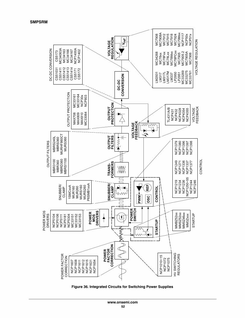
SMPSRM
www.onsemi.com 52
Figure 36. Integrated Circuits for Switching Power Supplies

SMPSRM
www.onsemi.com 53
Up to 25 W Flyback Switch−Mode Power Supply
Rectifier
ACLine
Bulk+StorageCapacitor
Start−upSwitch
PWMControl
ICProg.Prec.Ref
+Ultrafast
MOSFET
LoadRectifier
n−outputs
PWM Switcher
Figure 37. Up to 25 W Flyback
Table 1. High Voltage Switching Regulator Selection
Product Description
Technical Documentation and Design Resources
AppNotes
Design &Development
ToolsDesignNotes
EvalBoard
ReferenceDesigns Videos
WhitePapers
NCP1014High Voltage Switching Regulatorfor Offline SMPS � � � � � � �
NCP1013High Voltage Switching Regulatorfor Offline SMPS � � � �
NCP1012High Voltage Switching Regulatorfor Offline SMPS � � � �
NCP1072High Voltage Switching Regulatorfor Offline SMPS � � �
NCP1075High Voltage Switching Regulatorfor Offline SMPS � � � �
NCP1011High Voltage Switching Regulatorfor Offline SMPS � � �
NCP1010High Voltage Switching Regulatorfor Offline SMPS � �
Table 2. PWM Switching Controllers Selection
Product Description
Technical Documentation and DesignResources
AppNotes
Design &Development
ToolsDesignNotes
EvalBoard
NCP1250 PWM Controller, Current Mode, for Offline Power Supplies � � � �
NCP1251 PWM Controller, Current Mode, for Offline Power Supplies � � � �
NCP1253 PWM Controller, Current Mode, for Offline Power Supplies �

SMPSRM
www.onsemi.com 54
25 to 150 W Flyback Switch−Mode Power Supply
Rectifier
ACLine
Bulk+StorageCapacitor
Start−upSwitch
PWMControl
ICProg.Prec.Ref
+Ultrafast
MOSFET
LoadRectifier
n−outputs
PWM Switcher
Figure 38. 25 to 150 W Flyback
Table 3. Fixed Frequency Switching Controllers Selection
Product Description
Technical Documentation and Design Resources
AppNotes
Design &Development
ToolsDesignNotes
EvalBoard Videos
NCP1219PWM Controller with Adjustable Skip Level and ExternalLatch Input � � � �
NCP1234Controller, Fixed Frequency, Current Mode, for FlybackConverters �
NCP1236Controller, Fixed Frequency, Current Mode, for FlybackConverters � �
NCP1244Controller, Fixed Frequency, Current Mode, for FlybackConverters
NCP1246Controller, Fixed Frequency, Current Mode, for FlybackConverters � �
NCP1249PWM Controller Featuring Peak Power Excursion and HVStartup � �
NCP1255PWM Controller, Current Mode, for Offline Power SuppliesFeaturing Peak Power Excursion � � �
NCP1271PWM Controller, Soft−Skip� Standby, with Adjustable SkipLevel and External Latch � � � �
NCP1927 PFC and Flyback Controller for Flat Panel TVs �
Table 4.Quasi−Resonant Switching Controllers Selection
Product Description
Technical Documentation and Design Resources
AppNotes
Design &Development
ToolsEval
BoardReferenceDesigns Videos
NCP1336Controller, Quasi−Resonant, Current Mode, with HVStart−Up
NCP1337Controller, Quasi−Resonant Current Mode, withOverpower Compensation � � � � �

SMPSRM
www.onsemi.com 55
Table 4.Quasi−Resonant Switching Controllers Selection
Product
Technical Documentation and Design Resources
DescriptionProduct VideosReferenceDesigns
EvalBoard
Design &Development
ToolsApp
NotesDescription
NCP1338PWM Controller, Free Running Quasi−ResonantCurrent Mode � � �
NCP1377Controller, Free Running Quasi−Resonant CurrentMode � �
NCP1379 Controller, Quasi−Resonant, Current Mode � �
NCP1380 Controller, Quasi−Resonant, Current Mode � � � �
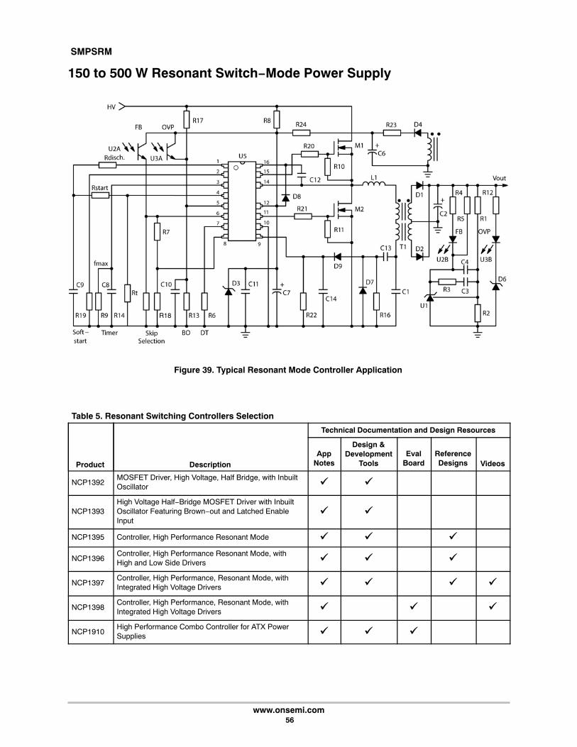
SMPSRM
www.onsemi.com 56
150 to 500 W Resonant Switch−Mode Power Supply
R18
Figure 39. Typical Resonant Mode Controller Application
Table 5. Resonant Switching Controllers Selection
Product Description
Technical Documentation and Design Resources
AppNotes
Design &Development
ToolsEval
BoardReferenceDesigns Videos
NCP1392MOSFET Driver, High Voltage, Half Bridge, with InbuiltOscillator � �
NCP1393High Voltage Half−Bridge MOSFET Driver with InbuiltOscillator Featuring Brown−out and Latched EnableInput
� �
NCP1395 Controller, High Performance Resonant Mode � � �
NCP1396Controller, High Performance Resonant Mode, withHigh and Low Side Drivers � � �
NCP1397Controller, High Performance, Resonant Mode, withIntegrated High Voltage Drivers � � � �
NCP1398Controller, High Performance, Resonant Mode, withIntegrated High Voltage Drivers � � �
NCP1910High Performance Combo Controller for ATX PowerSupplies � � �
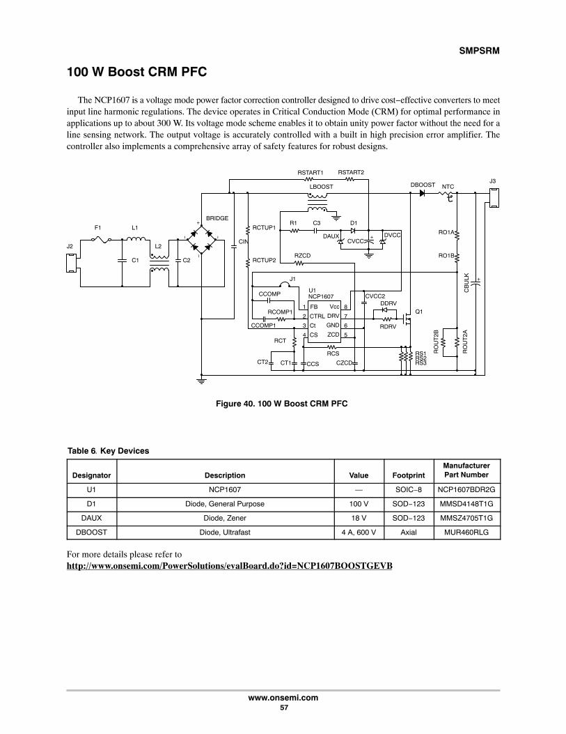
SMPSRM
www.onsemi.com 57
100 W Boost CRM PFC
The NCP1607 is a voltage mode power factor correction controller designed to drive cost−effective converters to meetinput line harmonic regulations. The device operates in Critical Conduction Mode (CRM) for optimal performance inapplications up to about 300 W. Its voltage mode scheme enables it to obtain unity power factor without the need for aline sensing network. The output voltage is accurately controlled with a built in high precision error amplifier. Thecontroller also implements a comprehensive array of safety features for robust designs.
Figure 40. 100 W Boost CRM PFC
C3
DBOOST
CIN
D1
CVCC2
+
CB
ULK
+CVCC
RDRV
RS1
U1NCP1607
5ZCD
3 Ct 6GND
4 CS
8Vcc
7DRV
1 FB
2 CTRL
RO1B
J3
J1
F1
C2
Q1
DAUX
RZCD
+−
~ ~BRIDGE
tNTC
RCT
RCTUP1
RCTUP2
RO1A
J2
CZCD
L1DVCC
CCOMP1
CT1
RO
UT
2A
CT2
RO
UT
2B
RCS
CCS
RSTART1
R1
RSTART2
RS2RS3
DDRV
C1
RCOMP1
CCOMP
L2
LBOOST
Table 6. Key Devices
Designator Description Value FootprintManufacturerPart Number
U1 NCP1607 — SOIC−8 NCP1607BDR2G
D1 Diode, General Purpose 100 V SOD−123 MMSD4148T1G
DAUX Diode, Zener 18 V SOD−123 MMSZ4705T1G
DBOOST Diode, Ultrafast 4 A, 600 V Axial MUR460RLG
For more details please refer tohttp://www.onsemi.com/PowerSolutions/evalBoard.do?id=NCP1607BOOSTGEVB
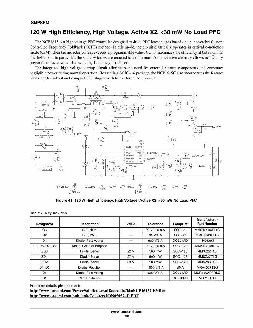
SMPSRM
www.onsemi.com 58
120 W High Efficiency, High Voltage, Active X2, <30 mW No Load PFC
The NCP1615 is a high voltage PFC controller designed to drive PFC boost stages based on an innovative CurrentControlled Frequency Foldback (CCFF) method. In this mode, the circuit classically operates in critical conductionmode (CrM) when the inductor current exceeds a programmable value. CCFF maximizes the efficiency at both nominaland light load. In particular, the standby losses are reduced to a minimum. An innovative circuitry allows near unitypower factor even when the switching frequency is reduced.
The integrated high voltage startup circuit eliminates the need for external startup components and consumesnegligible power during normal operation. Housed in a SOIC−16 package, the NCP1615C also incorporates the featuresnecessary for robust and compact PFC stages, with few external components.
Figure 41. 120 W High Efficiency, High Voltage, Active X2, <30 mW No Load PFC
C2
220 nF/X2
C1
100 nF/X2
L214
23
L1
150
uH
12
R1 R2
N/AN /A
470 V
RV1C4
1nF/Y2
C3
1nF/Y2
F1
3A
1 23
J1
A
B
+
�
C5
470
nF1
1HS
1
R4
1k
R31k
12
12
D1
D2
MR
A40
07
MR
A40
07
HV
VIN
1N5406
MUR550
D4
D5
21
21
VAUX
L3200 uH
C16R26 1k
R5
4.7k
2D
3
MM
SD
4148
1
100 pF
R6
N/AR7
4.7k
15
RT1
R8
80 m
/ 3
W
Q1IPA50R250 22
3R9
10k
1
3
R10
2.2
Q2
MMSD4148
D6 2 R11
22
1
1
2
3
DRV
HV
PFCOK
R21 68
1k
C15
0.1
uF
R22
1.8M
eg
R23
1.8M
egR
20 N/A
C6
100
uF/4
50 V
21
J21
2
R24
1k
R25
1kSTBY
R27
1k
Q3
STDBY
PPCOK
1
3
2
R17 0
R18 27
kC
14
1nF
STDBY
DRV
VCC
ZD
1
26 V
21
220k
RT
2
PSM
C7
2.2
uF
R12 27
kC
8
220
nFR
13 270k
R14
C9
220
nF12
0kC
10
10 u
FR
15
4.99
Meg
VCCEXT_VCC
VAUX
C11
220
nFC
12
220
uF/5
0 V
21
ZD
2
33 V
21
ZD
3
22 V
21
2D
71
MM
SD
4148
D821
MMSD4148
C13
10 nF
R16
27
16
10
11
7
5
6
9
1
2
3
4
8
14
13
12
PFCOKPFCOK
CS/ZCD
FAULT
VCONTROL
FFCONTROL
PSTIMER
HV HVFB
FB
RESTART
FOVP/BUV
STDBY
VCC
DRV
GND
PFCOKTP1
PFCOKVIN
TP3
VinSTBY
TP2
STBYHV
TP4
HV
Ext. VCC
EXT_VCC1
2
J3
Ext. VCC
PSM1
2
J4
Table 7. Key Devices
Designator Description Value Tolerance FootprintManufacturerPart Number
Q3 BJT, NPN — ?? V/200 mA SOT−23 MMBT3904LT1G
Q2 BJT, PNP — 30 V/1 A SOT−23 MMBT589LT1G
D4 Diode, Fast Acting — 600 V/3 A DO201AD 1N5406G
D3, D6, D7, D8 Diode, General Purpose — ?? V/200 mA SOD−123 MMSD4148T1G
ZD3 Diode, Zener 22 V 500 mW SOD−123 MMSZ22T1G
ZD1 Diode, Zener 27 V 500 mW SOD−123 MMSZ27T1G
ZD2 Diode, Zener 33 V 500 mW SOD−123 MMSZ33T1G
D1, D2 Diode, Rectifier — 1000 V/1 A SMA MRA4007T3G
D5 Diode, Fast Acting — 520 V/5 A DO201AD MUR550APFRLG
U1 PFC Controller — — SO−16NB NCP1615C
For more details please refer tohttp://www.onsemi.com/PowerSolutions/evalBoard.do?id=NCP1615GEVB orhttp://www.onsemi.com/pub_link/Collateral/DN05057−D.PDF
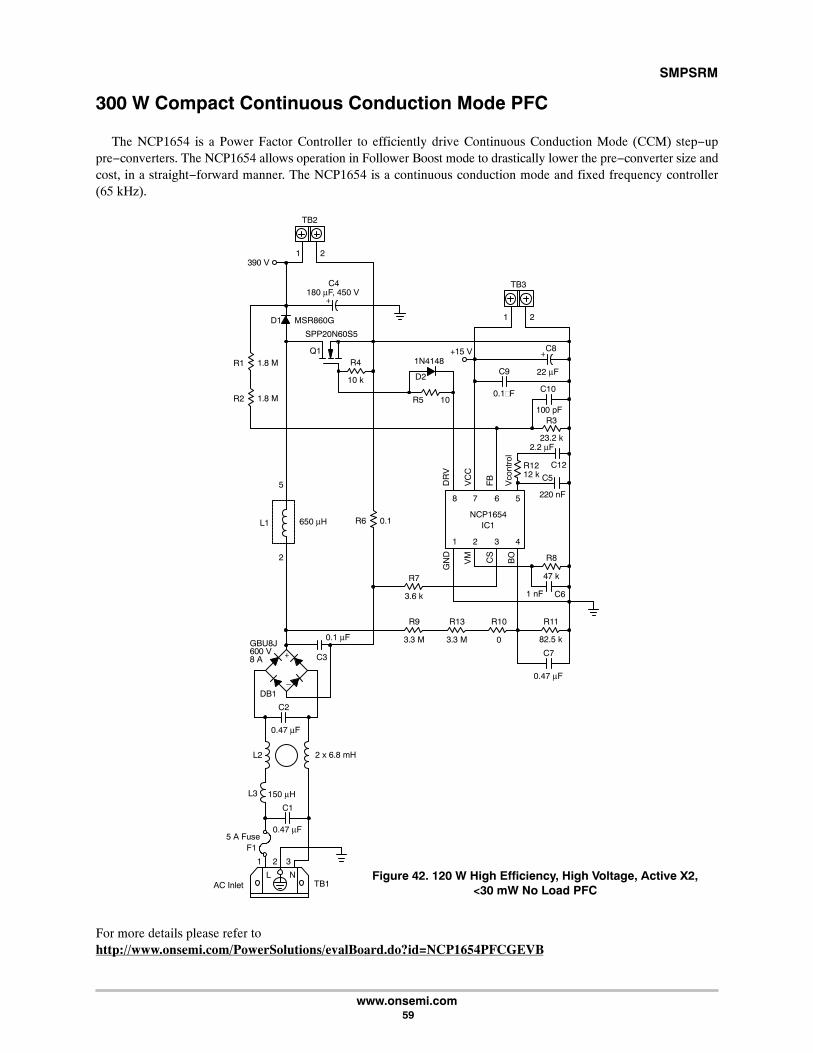
SMPSRM
www.onsemi.com 59
300 W Compact Continuous Conduction Mode PFC
The NCP1654 is a Power Factor Controller to efficiently drive Continuous Conduction Mode (CCM) step−uppre−converters. The NCP1654 allows operation in Follower Boost mode to drastically lower the pre−converter size andcost, in a straight−forward manner. The NCP1654 is a continuous conduction mode and fixed frequency controller(65 kHz).
Figure 42. 120 W High Efficiency, High Voltage, Active X2,<30 mW No Load PFC
TB2
390 V
R1
R2
1.8 M
1.8 M
+
C4
1 2
D1 MSR860G
Q1
SPP20N60S5
R4
10 k
R5 10
D2
1N4148
TB3
+15 V +
21
C8
C9
0.1�F C10
100 pFR3
23.2 k
C12
C5
220 nF
NCP1654
R8
47 k
C61 nF
R11
82.5 k
C7
R10
0
R13
3.3 M
R9
3.3 M
R7
3.6 k
5
2
L1 R6 0.1
C3
DB1
C2
2 x 6.8 mHL2
L3
C1
5 A FuseF1
AC InletL N
1
TB1
2 3
IC1
1 2 3 4
8 7 6 5
GN
D
VM CS
BO
DR
V
VC
C
FB
Vco
ntro
l
R1212 k
+
�
GBU8J
8 A600 V
180 μF, 450 V
22 μF
2.2 μF
0.47 μF
0.47 μF
0.47 μF
150 μH
0.1 μF
650 μH
For more details please refer tohttp://www.onsemi.com/PowerSolutions/evalBoard.do?id=NCP1654PFCGEVB
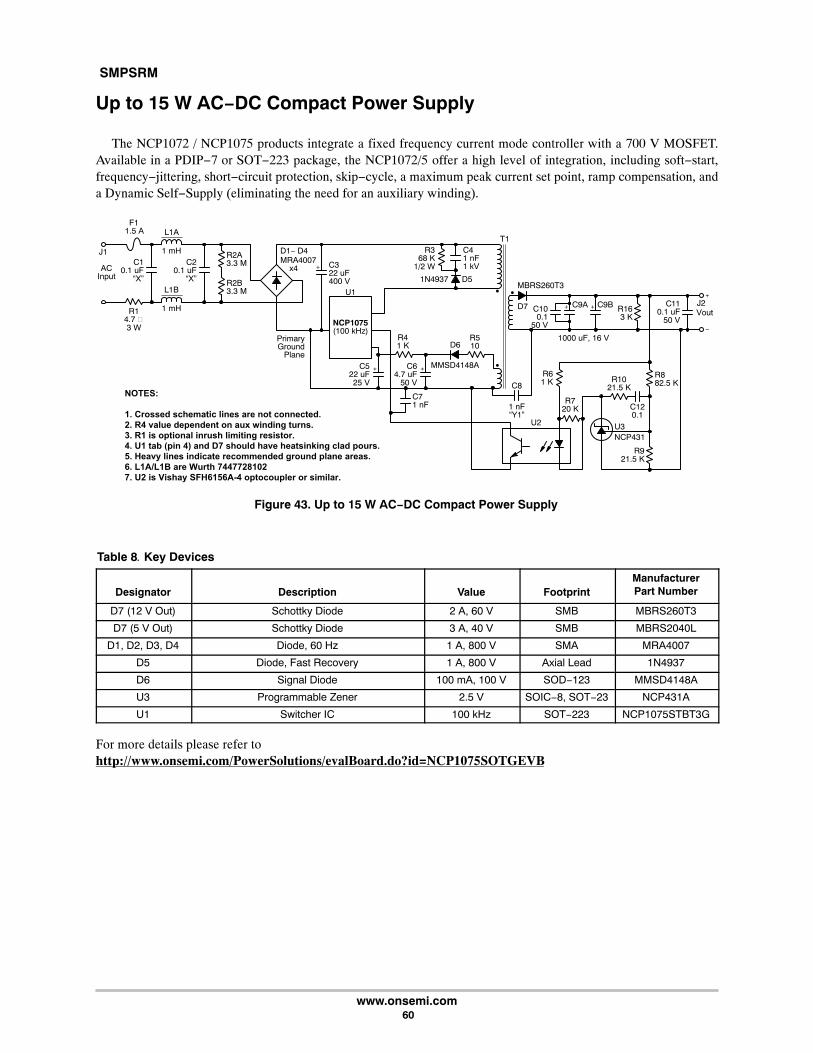
SMPSRM
www.onsemi.com 60
Up to 15 W AC−DC Compact Power Supply
The NCP1072 / NCP1075 products integrate a fixed frequency current mode controller with a 700 V MOSFET.Available in a PDIP−7 or SOT−223 package, the NCP1072/5 offer a high level of integration, including soft−start,frequency−jittering, short−circuit protection, skip−cycle, a maximum peak current set point, ramp compensation, anda Dynamic Self−Supply (eliminating the need for an auxiliary winding).
NOTES:
1. Crossed schematic lines are not connected.
2. R4 value dependent on aux winding turns.
3. R1 is optional inrush limiting resistor.
4. U1 tab (pin 4) and D7 should have heatsinking clad pours.
5. Heavy lines indicate recommended ground plane areas.
6. L1A/L1B are Wurth 7447728102
7. U2 is Vishay SFH6156A-4 optocoupler or similar.
1N4937
MRA4007 x4
MMSD4148A
NCP431
D5
C41 nF1 kV
T1
C20.1 uF
“X”
R2A3.3 M
R2B3.3 M
1 mH
L1AF1
1.5 A
ACInput
J1
R14.7 �3 W
1 mH
L1B
D1− D4 R368 K
1/2 W
D6R510
R41 K
C10.1 uF
“X”
C322 uF400 V
U1
C522 uF25 V
PrimaryGround
Plane
R720 K
R1021.5 K
C120.1
R61 K
R882.5 K
C64.7 uF
50 V
C71 nF
MBRS260T3
D7 C100.1
50 V
1 nF“Y1”
C8
U2 U3
1000 uF, 16 V
C9A C110.1 uF
50 V
C9B R163 K
R921.5 K
VoutJ2
NCP1075(100 kHz)
Figure 43. Up to 15 W AC−DC Compact Power Supply
Table 8. Key Devices
Designator Description Value FootprintManufacturerPart Number
D7 (12 V Out) Schottky Diode 2 A, 60 V SMB MBRS260T3
D7 (5 V Out) Schottky Diode 3 A, 40 V SMB MBRS2040L
D1, D2, D3, D4 Diode, 60 Hz 1 A, 800 V SMA MRA4007
D5 Diode, Fast Recovery 1 A, 800 V Axial Lead 1N4937
D6 Signal Diode 100 mA, 100 V SOD−123 MMSD4148A
U3 Programmable Zener 2.5 V SOIC−8, SOT−23 NCP431A
U1 Switcher IC 100 kHz SOT−223 NCP1075STBT3G
For more details please refer tohttp://www.onsemi.com/PowerSolutions/evalBoard.do?id=NCP1075SOTGEVB

SMPSRM
www.onsemi.com 61
25 W Offline Power Supply High Voltage Switcher
The NCP1129 switcher offers everything needed to build reliable and compact AC−DC switching power supplieswith minimal surrounding elements. Incorporating an avalanche rated 650 V MOSFET, converters built with theNCP112X can be safely designed for international conditions without jeopardizing the overall reliability. The NCP112Ximplements peak current mode control with adjustable ramp compensation that ensures stability in ContinuousConduction Mode (CCM) operation. With an external resistor, the maximum peak current is adjustable, allowing thedesigner the ability to inject ramp compensation to stabilize CCM power supplies.
Figure 44. 25 W Offline Power Supply High Voltage Switcher
1N4937
MRA4007 x4
1N4937
NCP431
D5
C410 nF1 kV
T1
C20.1 uF“X2”
R41 M
R51 M
0.5 W
L1A820 uH
R25.6 KF1
2 A250 Vac
ACInput
J1
R14.7 �3 W
L1B820 uH
D1− D4 R847 K1 W
D7R122.0
R110 Ohms
C7100 pF R9A/B
0.5 W
1 Ohm x 2
R102.4 K
R73 M0.5 W
C61 nF
Z125 V
C54.7 uF
R35.6 K
R65.6 K
C10.1 uF
“X2”
C347 uF400 V U1
NU
VCC
FB
GND
S
Is
D
R1515 K
R1620 K
C120.1
R141 K
R1739 K
C64.7 uF
50 V
D8(TO−220)
C140.1
1 nF“Y1”
C13
U2 U3
1000 uF, 16 V
C9A C110.1 uF
50 V
C9B
R1810 K
VoutJ2C9C
D6MMSD4148A
NCP1129
R1333
C101 nF
Table 9. Key Devices
Designator Description Value FootprintManufacturerPart Number
D8 Schottky Diode 20 A, 100 V TO−220 NTST20100CTG
D1, D2, D3, D4 Diode, 60 Hz 1 A, 800 V SMA MRA4007
D5, D7 Diode, Fast Recovery 1 A, 600 V Axial Lead 1N4937
D6 Signal Diode 100 mA, 100 V SOD−123 MMSD4148A
Z1 (Optional) Zener Diode 25 V SOD−123 MMSZ5253B
U3 Programmable Zener 2.5 V SOT−23 NCP431A
U1 Controller 65 kHz DIP−8 NCP1129
For more details please refer tohttp://www.onsemi.com/PowerSolutions/evalBoard.do?id=NCP1129DIPGEVB
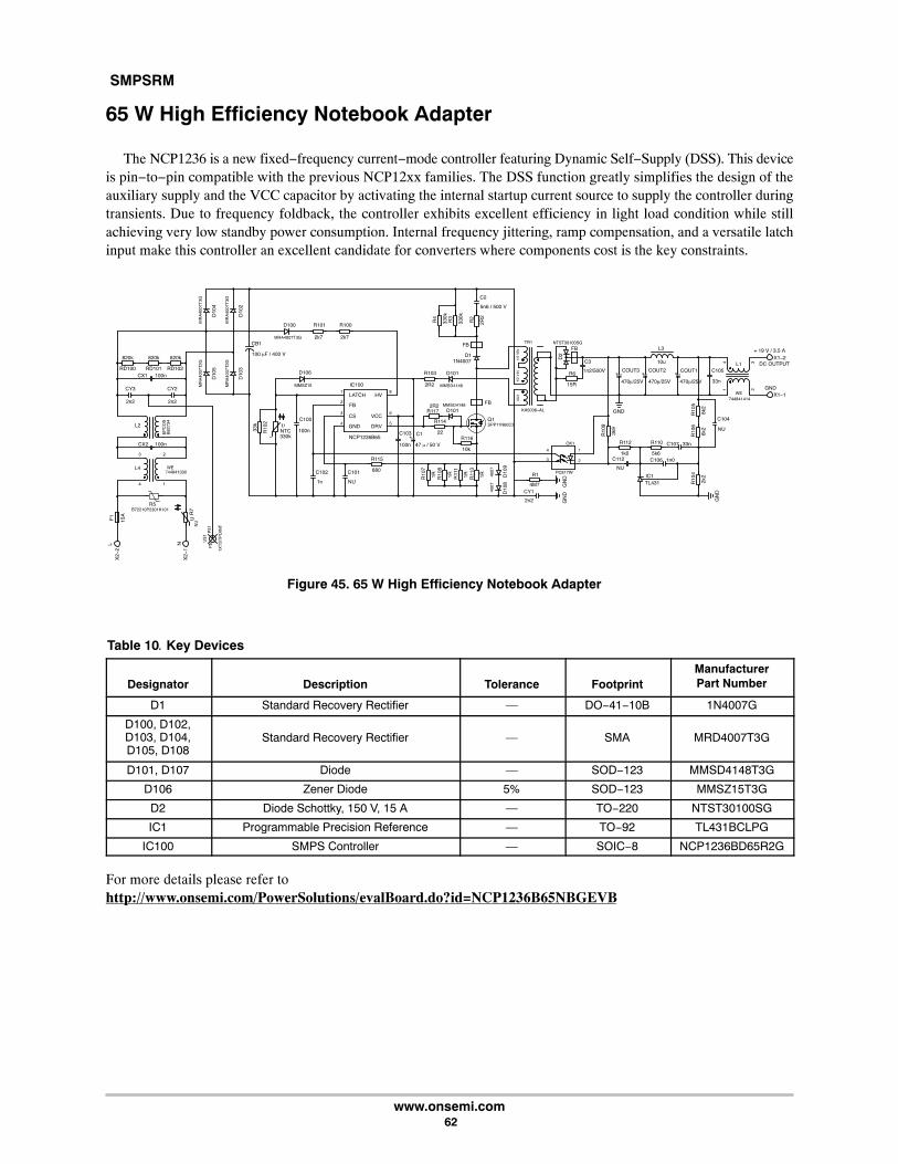
SMPSRM
www.onsemi.com 62
65 W High Efficiency Notebook Adapter
The NCP1236 is a new fixed−frequency current−mode controller featuring Dynamic Self−Supply (DSS). This deviceis pin−to−pin compatible with the previous NCP12xx families. The DSS function greatly simplifies the design of theauxiliary supply and the VCC capacitor by activating the internal startup current source to supply the controller duringtransients. Due to frequency foldback, the controller exhibits excellent efficiency in light load condition while stillachieving very low standby power consumption. Internal frequency jittering, ramp compensation, and a versatile latchinput make this controller an excellent candidate for converters where components cost is the key constraints.
Figure 45. 65 W High Efficiency Notebook Adapter
Table 10. Key Devices
Designator Description Tolerance FootprintManufacturerPart Number
D1 Standard Recovery Rectifier — DO−41−10B 1N4007G
D100, D102,D103, D104,D105, D108
Standard Recovery Rectifier — SMA MRD4007T3G
D101, D107 Diode — SOD−123 MMSD4148T3G
D106 Zener Diode 5% SOD−123 MMSZ15T3G
D2 Diode Schottky, 150 V, 15 A — TO−220 NTST30100SG
IC1 Programmable Precision Reference — TO−92 TL431BCLPG
IC100 SMPS Controller — SOIC−8 NCP1236BD65R2G
For more details please refer tohttp://www.onsemi.com/PowerSolutions/evalBoard.do?id=NCP1236B65NBGEVB
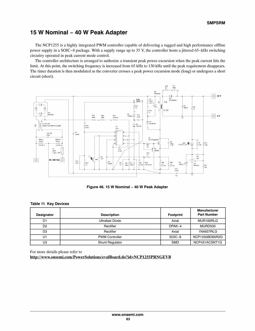
SMPSRM
www.onsemi.com 63
15 W Nominal − 40 W Peak Adapter
The NCP1255 is a highly integrated PWM controller capable of delivering a rugged and high performance offlinepower supply in a SOIC−8 package. With a supply range up to 35 V, the controller hosts a jittered 65−kHz switchingcircuitry operated in peak current mode control.
The controller architecture is arranged to authorize a transient peak power excursion when the peak current hits thelimit. At this point, the switching frequency is increased from 65 kHz to 130 kHz until the peak requirement disappears.The timer duration is then modulated as the converter crosses a peak power excursion mode (long) or undergoes a shortcircuit (short).
19
16
C133nF
21
R120
6
10
22
R2a1.5
18
R101k
15
3
R12.2k
17 14R622
Q22N2907
11
R151k
C4220pF
31
R16331k
4
C51nF
C1047p
C8100p
Q1ST P7Nk80ZFP
12 30
R1880
24
C11680p
D2M URD530
D1M UR160
44
33
D31N4937
R24not wi red
C2680uF R3
1k
20
R74.3k
U2B
R2b1.5
C7100uF
32 V
0 V
U2A
36
U3NCP431 R11
10k
R17118k
C922n
1
2
3
4 5
8
6
7
5
13
U1Eri s
R580k
C61u
1
23 25
26
C12470n
35
2 x 27 mH
+ −
IN
Schaf f ner RN114−0.8/02
IC4
L1
KBU406
X2
85−260 VacC310uF
27
R142.2M eg
34
R19820k
C13
.
47uF
D41N4148
aux.
R20390k
F1250VT ype = 2AT
1 kV
2 0 0 V
D51N973
S FH−6 1 5 A
0 .5 W0 .5 W
1
6 7,8
11,12
2 5
C142.2nF
Y1
3 x3 30 k 3 x3 30 k
R9ab c1M eg
R35a bc1M eg
C150.1uF
R1310
D6P6KE220
.
.
Figure 46. 15 W Nominal − 40 W Peak Adapter
Table 11. Key Devices
Designator Description FootprintManufacturerPart Number
D1 Ultrafast Diode Axial MUR160RLG
D2 Rectifier DPAK−4 MURD530
D3 Rectifier Axial 1N4937RLG
U1 PWM Controller SOIC−8 NCP1255BD65R2G
U3 Shunt Regulator SMD NCP431ACSNT1G
For more details please refer tohttp://www.onsemi.com/PowerSolutions/evalBoard.do?id=NCP1255PRNGEVB

SMPSRM
www.onsemi.com 64
220 W LED−TV Design Power Supply
The NCP1398 is a high performance controller for half bridge LLC resonant converters. The integrated high voltagegate driver simplifies layout and reduces external component count. A unique architecture, which includes a 750 kHzVoltage Controlled Oscillator whose control mode permits flexibility when an ORing function is required allows theNCP1398 to deliver everything needed to build a reliable and rugged resonant mode power supply.
In association with NCP1607/08 CRM Boost PFC Controller and NCP1027 high integrated HV switching regulatorthey offer a complete solution.
AC1 AC2
−+
VCCR.CBOFB D
OPPGND
P$1
P$4
P$8
P$5
P$2
P$3
FBCOMP
GND
VCC
ZCD
DRVMULTCS
3
21
4
3
21
4
1
23
4
1
23
4
1
23
4
BOCTIMERDISCHFMAXRTDTFBSKIP/DIS OLP
MLOWGNDVCC
MUPPHB
VBOOT
P$1
P$4
P$8
P$5
P$2
P$3
Figure 47. 220 W LED−TV Design Power Supply
Table 12. Key Devices
Designator Description Tolerance FootprintManufacturerPart Number
D1, D11, D12, D13 Switching Diode — SOD−123 MMSD4148T3G
D2 Standard Recovery Rectifier — Axial Lead 1N5408RLG
D3, D5, D6, D7, D8, D9 Diode — SMC MBRS4201T3G
D4 Soft Recovery Rectifier — TO−220FP MSRF860G
D10 Schottky Rectifier — TO−220FP MBRF20100CTG
D17 Diode — SMC MBRS320T3G
D19 Zener Diode 5% SOD−123 MMSZ16T1G
IC1 PFC Controller — SOIC−8 NCP1607BDR2G
IC2, IC5 Programmable Precision Reference — TO−92 TL431BCLPG
IC3 Resonant Controller — SOIC−16 NCP1398BDR2G
IC4 HV Switcher for Medium Power Offline SMPS — PDIP−8 NCP1027P065G
For more details please refer tohttp://www.onsemi.com/PowerSolutions/evalBoard.do?id=NCP1398LCDGEVB

SMPSRM
www.onsemi.com 65
High Efficiency and Below 10 mW Standby PFC + QR Combo Chip for90 W SMPS
This combination IC integrates power factor correction (PFC) and quasi−resonant flyback functionality necessary toimplement a compact and highly efficient Switched Mode Power Supply for an adapter application.
The PFC stage exhibits near−unity power factor while operating in a Critical Conduction Mode (CrM) with amaximum frequency clamp. The circuit incorporates all the features necessary for building a robust and compact PFCstage while minimizing the number of external components.
The quasi−resonant current−mode flyback stage features a proprietary valley−lockout circuitry, ensuring stable valleyswitching. This system works down to the 4th valley and toggles to a frequency foldback mode with a minimumfrequency clamp beyond the 4th valley to eliminate audible noise.
Figure 48. High Efficiency 90 W SMPS Based on NCP1937
3
1
2
M3
IPP045N10N3C19
1000u
1 VCC
2 MIN_TOFF
3 MIN_TON
4 TRIG/DIS 5CS
6COMP
7GND
8DRV
U5
NCP4304
C22
0.22u
R28
20
R29
15k
R30
15k
R31
0
R32267
R33
453k
R34
90.9k
1VSNS
2OFFDET
3VMIN
4LED5 ON/OFF
6 FBC
7 GND
8 VCC
U4 NCP4355
C23
0.47u
C24 0.1u
R35
200k
R37
14.3k
R36
14.3kR38
2.32k
R39
1k
C26
22n
J2
C20
1000u
2
1
D12
MM
SD103T1
21
D13MMSD103T1
CX10.1u
F1
3A
C1
0.22u
C2
0.22u
432 1
L2
3
1
2
M1
TK12A60U
R3
0.5
R3A
0.5
R4
10k
R6
8.06k
R7
47.5
R8
4.7
5
C5
6800p
3
12
M2
IPA65R380C6
21
R10
20
C6
100p
R12
10k
R13
0.4
R13A
0.4
R14
249
1
2
3
J1
R1 1k
R15
1.62 MEG
R16
1.62 MEG
R17
118k
R18 34k
C10
1nC8
47u
C11
0.1u
C12 100n
C13 2.2u R19 20k
C14 330p
R20 499k
C15 150p
R21
0
C16
0.47u
R24
80.6k
C17
100p
C18
47p
R25
2k
R26
1 MEG
R27
2k
C27
10nRT1
220k
C9
4.7p
R5010k
R9
20
C28 100u
R52TBD
C29TBD
R41
10
21
D9
MMSD414821
D10
MMSD4148
21D11
MMSD4148
21
D5
MM
SD4148
D14
MM
SZ5254
123
4
U2
123
4
U3
R44
100k
R2 1k
L3
300u
2
1
D1
MRA4007
2
1
D2
MRA4007
2 1
D3
1N5406
C3
82u
R45
100k
R3B
0.5
R3C
0.5
112
58
3 10
21
94
11
L4
C7TBD
(Aux)
3
1
4
96
10
8
7
11
TX1
500u
CY3
1000p
R40
0
2 1
D4
MUR550
1 1
2 2
3 3
HS1
Custom
1 1
2 2
HS2
Custom
D15
MBR5H100MFS
1 HVX2
3 BOX2
9 PSTIMER
10 QFB 11QZCD
5 PCONTROL
6 PONOFF
7 QCT
8 FAULT
17GND
18PFBLV
20PFBHV
12VCC
13QCS
14QDRV
15PDRV
16PCS/PZCD
U1
NCP1937
1+2 ~A
3 ~B 4-
D16
GBU406
R43
100kR42
100k
C4
10n
C21
47n
C25
1u
R4920
R51
10k
Q1 BSS84
21
D18MMSD103T1
R53
35.7kD17
MMSZ5236
RT2
15
21
D19
MMSD4148
432 1
L1
CY11000p
CY2
1000p
CX2
0.1u
MOV1
S10K300
D7
S2M
C32 33p
R23
750k
C30 10u
C31
TBD
R22
5.11 MEG
R58.06k
21
D6
MMSD41482
1
D8
MM
SD4148
21
R11
8.2
5
VAUX
VAUX
QFB
QFB
PSTIMER
PSTIMER
VOUTA
VOUTA
VBULK
MIN_TOFF
MIN_TOFF
U4_VCC
U4_VCC
VCC
VCC
Table 13. Key Devices
Designator Description Value FootprintManufacturerPart Number
D1, D2 Diode, Standard Recovery 1000 V, 1 A SMD, SMA MRA4007T3G
D3 Diode, Standard Recovery, Vertical Mount,Teflon Tube Required on Exposed Lead 600 V, 3 A DO−201AA 1N5406G
D4 Diode, Switch−mode Rectifier, Vertical Mount,Teflon Tube Required on Exposed Lead 520 V, 5 A DO−201AA MUR550APFG
D5, D6, D8, D9, D10, D11,D19 Diode, Switching 100 V, 200 mA SMD, SOD−123 MMSD4148T1G
D12, D13, D18 Diode, Switching 250 V, 100 mA SMD, SOD−123 MMSD103T1G
D14 Diode, Zener 27 V, 500 mW SMD, SOD−123 MMSZ5254BT1G
D15 Diode, Schottky 100 V, 5 A SMD, SO−8FL MBR5H100MFST1G
D17 Diode, Zener 7.5 V, 500 mW SMD, SOD−123 MMSZ5236BT1G
U1 Controller, PFC−QR Combo — SMD, SOIC−20NB NCP1937A1
U4 Controller, Sleepmode, Secondary Side — SOIC−8 NCP4355B
U5 Synchronous Rectification Driver — SOIC−8 NCP4304A
For more details please refer tohttp://www.onsemi.com/PowerSolutions/evalBoard.do?id=NCP1937BADAPGEVB
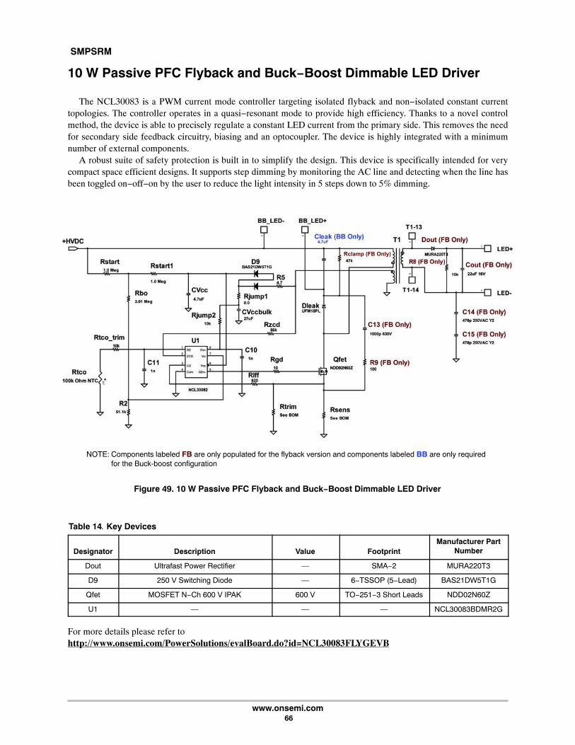
SMPSRM
www.onsemi.com 66
10 W Passive PFC Flyback and Buck−Boost Dimmable LED Driver
The NCL30083 is a PWM current mode controller targeting isolated flyback and non−isolated constant currenttopologies. The controller operates in a quasi−resonant mode to provide high efficiency. Thanks to a novel controlmethod, the device is able to precisely regulate a constant LED current from the primary side. This removes the needfor secondary side feedback circuitry, biasing and an optocoupler. The device is highly integrated with a minimumnumber of external components.
A robust suite of safety protection is built in to simplify the design. This device is specifically intended for verycompact space efficient designs. It supports step dimming by monitoring the AC line and detecting when the line hasbeen toggled on−off−on by the user to reduce the light intensity in 5 steps down to 5% dimming.
NOTE: Components labeled FB are only populated for the flyback version and components labeled BB are only requiredfor the Buck-boost configuration
Rclamp (FB Only)
Figure 49. 10 W Passive PFC Flyback and Buck−Boost Dimmable LED Driver
Table 14. Key Devices
Designator Description Value FootprintManufacturer Part
Number
Dout Ultrafast Power Rectifier — SMA−2 MURA220T3
D9 250 V Switching Diode — 6−TSSOP (5−Lead) BAS21DW5T1G
Qfet MOSFET N−Ch 600 V IPAK 600 V TO−251−3 Short Leads NDD02N60Z
U1 — — — NCL30083BDMR2G
For more details please refer tohttp://www.onsemi.com/PowerSolutions/evalBoard.do?id=NCL30083FLYGEVB

SMPSRM
www.onsemi.com 67
Additional Documentation
Table 15. Design NotesDocument Title Document ID
Compact 200−265 Vac HiPF Boost LED Driver DN05062/D
NCP1011: Efficient, Low Cost, Low Standby Power (<100 mW), 2.5 W CCCV Charger DN06017/D
NCP1012: 1 W, Dual Output, Off−line Converter DN06002/D
NCP1012: 3.6 W Auxiliary Power Supply for Appliances / White Goods DN06013/D
NCP1013: Universal Input, 5 W, LED Ballast DN06027/D
NCP1014, NSI45025: Universal Off−Line LED String Driver with PFC DN06065/D
NCP1014: 10 W, 3−Output Off−line Power Supply DN06005/D
NCP1014: 10 W, Dual Output Power Supply DN06020/D
NCP1014: 12 Watt Mini Boost Power Factor Corrector for LED applications DN06064/D
NCP1014: 5 V, 400 mA Current Boosted Buck Converter DN06052/D
NCP1014: 5 W, CCCV Cell Phone Battery Charger DN06009/D
NCP1014: 8 W Off−Line Non−Isolated Buck Regulator DN06011/D
NCP1014: 8 W, 3−Output Off−Line Switcher DN06003/D
NCP1014: Improving the Power Factor of Isolated Flyback Converters for Residential ENERGY STAR®
LED Luminaire Power SuppliesDN06051/D
NCP1014: Low Power, Off−Line Buck, CVCC Power Supply DN06037/D
NCP1014: Low Power, Off−Line, Constant Voltage Non−Isolated Power Supply DN06066/D
NCP1014: Universal Input, +/− 12 V Output, 8 Watt Power Supply DN06034/D
NCP1027: 1 A, 12 W Constant Current Off−Line LED Driver DN06006/D
NCP1027: 10 W, 24 V / 5 V Off−Line Power Supply DN06012/D
NCP1027: 16 W, 12 Vdc Modem Power Supply DN06021/D
NCP1028: Single Stage, Off−line, Isolated 12 V, 800 mA Converter with High Power Factor DN06069/D
NCP1050: Extremely Low AC−DC Power Supply Used with GFCI DN05037/D
NCP1055, MC33340: Universal AC 15 W charger for 4 NiMH/NiCd cells DN06023/D
NCP1055: 7 W, non−isolated buck ac−dc converter DN06028/D
NCP1055: Simple, 3 W, Non−isolated Bias Supply DN06053/D
NCP1071, NCP1075, MCP1077: 12 Vout, Off−line Buck Regulator DN05058/D
NCP1072: 10 W Primary Side Regulation (PSR) DN05036/D
NCP1075, NCP4328: Compact 90−135 Vac HiPF Boost LED Driver DN05055/D
NCP1075: Non−isolated, 8 W Dual Output, Off−line Power Supply DN05038/D
NCP1075: Universal AC Input, 12 Vout,10 W E−Meter Power Supply DN05018/D
NCP1076/7: Universal Input, 5 V or 12 V Output, up to 24 W Power Supply DN05049/D
NCP1077: 12 Vout, 6 W, Off−line Buck Regulator Using a Tapped Inductor DN05059/D
NCP1124 : 10 W Universal Input, 5 V output power supply DN05061/D
NCP1129: 12 W, Off−line Buck Regulator DN05053/D
NCP1129: Universal AC Input, 5 V or 12 V output, 20 W − White Goods/Industrial DN05043/D
NCP1136 : 5 V / 20 W Universal Input Power Supply (800 V MOSFET) DN05054/D
NCP1216: 24 V, Off−line Flyback Converter for Motor and Solenoid Applications DN06049/D
NCP1216: 7 W, 90−135 Vac, 500 mA LED Driver DN06050/D
NCP1217: 18 to 24 V, 85 W, Off−line PSU with Short Term, High Surge Current Capability DN06038/D
NCP1217: 200 W, single output power supply DN06010/D
NCP1217: Universal AC 40 W Programmable Output DN06024/D
NCP1219: Universal AC Input, Non−isolated, 6 W Electric Meter Buck Power Supply DN05014/D
NCP1236: 65 W Off−Line Adapter DN06074/D
NCP1251: 12 V, 30 W, Off−line Mini−Forward Converter DN05029/D

SMPSRM
www.onsemi.com 68
Table 15. Design Notes
Document Title Document ID
NCP1251: 20 W Flyback with Primary Side Regulation (PSR) DN05033/D
NCP1251: 20 W Output Offline Power Supply DN05012/D
NCP1251: 20 W Output Offline Power Supply Using Synchronous Output Rectification DN05028/D
NCP1251: A 24 Vin, 40 Watt, Low Cost, DC−to−DC Converter DN05032/D
NCP1251: Low Power, Ultra−Wide AC Input Range, Electric Meter Power Supply DN05017/D
NCP1251: Ultra Wide Input Triple Output 15 W (E−Meter) DN05039/D
NCP1271: Ultra−Wide Input Range Bias Power Supply DN06058/D
NCP1308, LM2575: Universal Input, 50 W, 5 Output Quasi−Resonant Flyback Converter DN06029/D
NCP1308: �18 V Dual Output Power Supply DN06008/D
NCP1308: 170 Vdc output, quasi−resonant power supply DN06014/D
NCP1615: High Efficiency, High Voltage, Active X2, <30mW no load PFC DN05057/D
NCP1927: 140 W LCD TV Power Supply DN05001/D
NCP1937: High Efficiency, <10 mW Standby PFC + QR Adapter DN05044/D
Table 16. TutorialsDocument Title Document ID Revision Revision Date
Thermal Runaway TND327/D 0 Feb, 2007
Achieving High Power Density Designs TND325/D 0 Sep, 2007
LED Lighting Definitions & Characteristics TND328/D 1 Sep, 2007
Standby Power Reduction Techniques TND324/D 1 Sep, 2007
SMPS Overview TND342/D 0 Jun, 2008
SMPS Topologies TND343/D 0 Jun, 2008
AD2 − Adapter Less than 75 W TND355/D 0 Oct, 2008
ATX − Designing High−Efficiency ATX Solutions TND356/D 0 Oct, 2008
FB1 − DC−DC Converters Feedback and Control TND352/D 0 Oct, 2008
MOF − Multi−Output Flyback Off−Line Power Supply TND351/D 0 Oct, 2008
PFC1 − Advanced Power Factor Correction TND344/D 0 Oct, 2008
QR − Analysis and Design of Quasi−Resonant Converters TND348/D 0 Oct, 2008
SIM − Simulating Power Supplies with SPICE TND349/D 0 Oct, 2008
TEL − DC−DC Telecom and Networking Solutions TND347/D 0 Oct, 2008
ADAP1 − Fixed Frequency Adapter with Very Low Power Consumption TND376/D 0 Nov, 2009
ADAP2 − QR Adapter Design TND377/D 0 Nov, 2009
AiO − 200 W Power Supply for All−in−One PC TND383/D 0 Nov, 2009
F2S − 2 Switch Forward Converter TND378/D 0 Nov, 2009
FB2 − The TL431 in Switching Power Supplies TND381/D 0 Nov, 2009
HB − Half−Bridge Drivers, a Transformer−Based Solution or an All−Silicon Drive TND379/D 0 Nov, 2009
LCD − AC−DC Power Architecture in LCD TV TND353/D 1 Nov, 2009
LED − Driving High Brightness LEDs in the General Lighting Marketplace TND345/D 2 Nov, 2009
MAG − Magnetics in Switched−Mode Power Supplies TND350/D 1 Nov, 2009
OVR − Overview of Efficient Power Supply Solutions TND357/D 1 Nov, 2009
PFC2 − Compensating a PFC Stage TND382/D 0 Nov, 2009
Electromagnetic Compatibility TND389/D 0 Dec, 2009
Switcher Efficiency and Snubber Design TND396/D 0 Dec, 2009

SMPSRM
www.onsemi.com 69
Table 17. Application NotesDocument Title Document ID
100 Watt Universal Input PFC Converter AND8106/D
19 V, 3 A, Universal Input AC−DC Adaptor Using NCP1271 AND8242/D
2 Switch−Forward Current Mode Converter with the NCP1252 AND8373/D
300 W, Wide Mains, PFC Stage Driven by the NCP1654 AND8324/D
300 W, Wide Mains, PFC Stage Driven by the NCP1653 AND8185/D
32 W, 32 V Universal Input AC−DC Printer Adapter using the NCP1237 AND8454/D
48 W, 24 V/7.5 V Universal Input AC−DC Printer Adapter Using the NCP1219 AND8393/D
5 Key Steps to Design a Compact, High−Efficiency PFC Stage using the NCP1611 AND9062/D
5 Key Steps to Design a Compact, High−Efficiency PFC State Using the NCP1612 AND9065/D
5.0 V, 2.0 A Flyback Converter AND8099/D
700 mA LED Power Supply Using Monolithic Controller and Off−Line Current Boosted (Tapped Inductor) Buck Converter AND8328/D
8 W DVD Power Supply with NCP1027 AND8262/D
90 W, Single Stage, Notebook Adaptor AND8209/D
90 W, Universal Input, Single Stage, PFC Converter AND8124/D
A 12V/40W Demonstrator with NCP1250 AND8486/D
A 160 W CRT TV Power Supply Using NCP1337 AND8246/D
A 30 W Power Supply Operating in A Quasi−Square Wave Resonant Mode AND8129/D
A 36 W Ballast Application with the NCP5181 AND8244/D
A 48 V/ 2 A High Efficiency, Single Stage, Isolated Power Factor Corrected Power Supply for LED Drivers and Telecom Power AND8394/D
A 5 V/2 A Standby Power Supply for INTEL Compliant ATX Applications AND8241/D
A 6 W/12 W Universal Mains Adapter with the NCP101X AND8142/D
A 60 W ac−dc Demonstrator with NCP1250 AND8468/D
A 70 W Low Standby Power Supply w/NCP120x Series AND8076/D
A 75 W TV Power Supply Operating in Quasi−square Wave Resonant Mode Using NCP1207 Controller AND8145/D
A 90 W/19V High Efficiency, Notebook Adapter Power Supply with Inherent Power Factor Correction AND8397/D
A Quasi−Resonant SPICE Model Eases Feedback Loop Designs AND8112/D
A Simple 12 Vout, 22 W, Off−line Forward Converter Using ON Semiconductor’s NCP1027/1028 Monolithic Switcher AND8489/D
A Simple DC SPICE Model for the LLC Converter AND8255/D
A Simple Low−Cost Non−Isolated Universal Input Off−Line Converter AND8078/D
Adjusting the Over Temperature Protection Trip Point in NCP1250−Based Adapters AND9057/D
An Innovative Approach to Achieving Single Stage PFC and Step−Down Conversion for Distributive Systems AND8147/D
An Off−Line, Power Factor Corrected, Buck−Boost Converter for Low Power LED Applications AND9043/D
Application Note for a 5.0 W to 6.5 W Power Over Ethernet (PoE) DC−DC Converter AND8247/D
Calculating External Components AND8332/D
Characteristics of Interleaved PFC Stages AND8355/D
Circuit Design and PCB Layout Guidelines for Designs Using the NCP108x AND9133/D
Compensating the Negative Voltage Spike on the NCP1250 OPP Pin AND9066/D
Compensation of a PFC Stage Driven by the NCP1654 AND8321/D
Conducted EMI Filter Design for the NCP1200 AND8032/D
Design of Active Clamp Forward of DC−DC Converter using NCP1562 AND8273/D
Design of a 65 W Adapter Utilizing the NCP1237 PWM Controller AND8461/D
Design of an Isolated 2 W Bias Supply for Telecom Systems Using the NCP1030 AND8119/D
Designing Converters with the NCP101X Family AND8134/D
Designing NCP1337 AND8266/D
Designing NCP1381 and NCP1382 in High Power AC−DC Adapters AND8240/D
Designing a High−Efficiency, 300−W, Wide Mains Interleaved PFC AND8354/D
Designing a Quasi−Resonant Adapter Driven by the NCP1380 AND8431/D
Determining the Free−Running Frequency for QR Systems AND8089/D
Evaluating the Power Capability of NCP101X Members AND8125/D
Four Key Steps to Design a Continuous Conduction Mode PFC Stage Using the NCP1653 AND8184/D
Four Key Steps to Design a Continuous Conduction Mode PFC Stage Using the NCP1654 AND8322/D

SMPSRM
www.onsemi.com 70
Table 17. Application Notes
Document Title Document IDFurther Improve the Low−Power Efficiency of Your NCP1631−Driven Interleaved PFC AND8456/D
Generating a 1.2 V Voltage Supply using the NCP102 Voltage Regulator AND8303/D
Graphical Data Test Circuits for the NCP1650 TND307/D
High Efficiency 8 Output, 60 W Set Top Box Power Supply Design AND8252/D
High Power PoE Applications AND8333/D
How to Choose Switching Controller for Design AND8205/D
Implementing Constant Current Constant Voltage AC Adapter by NCP1200 and NCP4300A AND8042/D
Implementing Cost Effective & Robust Power Factor Correction with NCP1607 AND8353/D
Implementing Cost Effective and Robust Power Factor Correction w/ the NCP1606 AND8282/D
Implementing NCP1207 in QR 24 W AC−DC Converter with Synchronous Rectifier AND8127/D
Implementing Power Factor Correction with the NCP1608 AND8396/D
Implementing Simple Brown−Out Solution for NCP101X Series AND8272/D
Implementing a 12 V /240 W Power Supply with the NCP4303B, NCP1605 and NCP1397B AND8460/D
Implementing a 310 W Power Supply with NCP1910, NCP4303 & NCP1027 AND8474/D
Implementing a DC/DC Single−Ended Forward Converter with the NCP1216A AND8161/D
Implementing a Medium Power AC−DC Converter with the NCP1395 AND8257/D
Implementing an LCD TV Power Supply with NCP1396A, NCP1605 & NCP1027 AND8293/D
Implementing an LCD TV Power Supply with the NCP1392B / 1606 / 1351B AND8344/D
Implementing the NCP1200 in Low−Cost AC/DC Converters AND8023/D
Implementing the NCP1200 in a 10 W AC/DC Wall Adapter AND8038/D
Implementing the NCP1605 to Drive the PFC Stage of a 19 V/8 A Power Supply AND8281/D
Increasing the Efficiency of Low Power Converters with Resonant Snubbers AND8296/D
Key Steps to Design an Interleaved PFC Stage Driven by the NCP1631 AND8407/D
Loop Control Design of an ac−dc Adapter Using the NCP1250 AND8453/D
Low Cost AC−DC 5.0 W Adapter with NCP1215 AND8128/D
Low−Cost 100 mA High−Voltage Buck and Buck−Boost Using NCP1052 AND8098/D
NCP101x LED Flasher with Luxeon V Star LED AND8224/D
NCP1230 Applications Note AND8154/D
NCP1252 Boost and CAT4026 LED Driver Board AND8478/D
NCP1255, a Controller with Peak Output Power Capability AND9115/D
NCP1381/NCP1382 Demonstration Board: 120 W Notebook Adapter AND8260/D
NCP1611/NCP1612 Tips and Tricks AND9077/D
NCP1650 Benchtop Assistance AND8084/D
Non−isolated Negative Output Buck AC/DC Converter AND8190/D
Non−isolated Positive Output Buck/Boost AC/DC Converter AND8191/D
Nonisolated Negative Output Buck/Boost AC/DC Convertor AND8225/D
Nonisolated Positive Output Buck AC/DC Converter AND8226/D
Offline Buck Converter with Tapped Inductor Improves Performance AND8318/D
Offline Converter Provides 5.0 Volt, 1.0 Amp Output for Small Electronic Equipment AND8019/D
Offline isolated power supply to drive 3 LEDs AND8136/D
Output Voltage Range Control in NCP1653 Driven PFC Stages AND8256/D
Performance Improvements to the NCP1012 Evaluation Board AND8132/D
Power Factor Correction Stages Operating in Critical Conduction Mode AND8123/D
Ramp Compensation for the NCP1200 AND8029/D
Safety Tests on a NCP1611−Based PFC Stage AND9064/D
Safety Tests on a NCP1612−Based PFC Stage AND9079/D
Simple Input Adapter Reverse Voltage Protection AND8203/D
Simple Secondary Side Vcc Source for Low Power CVCC Power Supplies AND8395/D
Small, Simple, PWM Buck Controller Can Replace High Current LDOs AND8170/D
Stability Analysis in Multiple Loop Systems AND8327/D
Synchronizing NCP1207 (NCP1377/B, NCP1378) AND8187/D

SMPSRM
www.onsemi.com 71
Table 17. Application Notes
Document Title Document IDThe LCD TV Standby Power Consumption Reduction AND8279/D
The NCP1250, a Versatile Tiny Controller for Offline Converters AND8469/D
Tips and Tricks for NCP1250 AND8488/D
Tips and Tricks to Build Efficient Circuits with NCP1200 AND8069/D
Understanding Loop Compensation with Monolithic Switchers AND8334/D
Understanding the LLC Structure in Resonant Applications AND8311/D
Understanding the Output Current Capability of DC−DC Buck Converters AND8117/D

SMPSRM/DPDF
ON Semiconductor and the ON logo are registered trademarks of Semiconductor Components Industries, LLC (SCILLC). SCILLC owns the rights to a number of patents, trademarks, copyrights, trade secrets, and other intellectual property. A listing of SCILLC’s product/patent coverage may be accessed at www.onsemi.com/site/pdf/Patent-Marking.pdf. SCILLC reserves the right to make changes without further notice to any products herein. SCILLC makes no warranty, representation or guarantee regarding the suitability of its products for any particular purpose, nor does SCILLC assume any liability arising out of the application or use of any product or circuit, and specifically disclaims any and all liability, including without limitation special, consequential or incidental damages. “Typical” parameters which may be provided in SCILLC data sheets and/or specifications can and do vary in different applications and actual performance may vary over time. All operating parameters, including “Typicals” must be validated for each customer application by customer’s technical experts. SCILLC does not convey any license under its patent rights nor the rights of others. SCILLC products are not designed, intended, or authorized for use as components in systems intended for surgical implant into the body, or other applications intended to support or sustain life, or for any other application in which the failure of the SCILLC product could create a situation where personal injury or death may occur. Should Buyer purchase or use SCILLC products for any such unintended or unauthorized application, Buyer shall indemnify and hold SCILLC and its officers, employees, subsidiaries, affiliates, and distributors harmless against all claims, costs, damages, and expenses, and reasonable attorney fees arising out of, directly or indirectly, any claim of personal injury or death associated with such unintended or unauthorized use, even if such claim alleges that SCILLC was negligent regarding the design or manufacture of the part. SCILLC is an Equal Opportunity/Affirmative Action Employer. This literature is subject to all applicable copyright laws and is not for resale in any manner.
LITERATURE FULFILLMENT: Literature Distribution Center for ON Semiconductor P.O. Box 5163, Denver, Colorado 80217 USA Phone: 303-675-2175 or 800-344-3860 Toll Free USA/Canada Fax: 303-675-2176 or 800-344-3867 Toll Free USA/Canada Email: [email protected]
N. American Technical Support: 800-282-9855 Toll Free USA/Canada.Europe, Middle East and Africa Technical Support:
Phone: 421 33 790 2910Japan Customer Focus Center Phone: 81-3-5817-1050
ON Semiconductor Website: www.onsemi.com
Order Literature: http://www.onsemi.com/orderlit
For additional information, please contact your local Sales Representative
PUBLICATION ORDERING INFORMATION
Sales and Design Assistance from ON Semiconductor
www.onsemi.com/salessupport
For a comprehensive listing of ON Semiconductor Sales Offices, please visit:
AMERICAS REP FIRMSAlabama Huntsville e-Components (256) 533-2444Brazil Countrywide Ammon & Rizos (+55) 11-4688-1960California Bay Area Electec (408) 496-0706
Southern California Tech Coast Sales (949) 305-6869Canada Eastern Canada Astec (905) 607-1444Connecticut Statewide Paragon Electronic Systems (603) 645-7630Florida Statewide e-Components (888) 468-2444Georgia Atlanta e-Components (888) 468-2444Illinois Hoffman Estates Stan Clothier Company (847) 781-4010Indiana Fishers Bear VAI (317) 570-0707Kansas Overland Park Stan Clothier Company (913) 894-1675Maine Statewide Paragon Electronic Systems (603) 645-7630Maryland Columbia Third Wave Solutions (410) 290-5990Massachusetts Statewide Paragon Electronic Systems (603) 645-7630Mexico Countrywide Ammon & Rizos (+55) 11-4688-1960Michigan St. Joseph Bear VAI (440) 526-1991Minnesota Eden Prairie Stan Clothier Company (952) 944-3456Missouri St. Charles Stan Clothier Company (636) 916-3777New Hampshire Statewide Paragon Electronic Systems (603) 645-7630New Jersey Statewide S.J. Metro (516) 942-3232New York Binghamton TriTech - Full Line Rep (607) 722-3580
Jericho S.J. Metro (516) 942-3232Rochester TriTech - Full Line Rep (585) 385-6500
North Carolina Raleigh e-Components (888) 468-2444Ohio Brecksville Bear VAI Technology (440) 526-1991Puerto Rico Countrywide e-Components (888) 468-2444Rhode Island Statewide Paragon Electronic Systems (603) 645-7630Vermont Statewide Paragon Electronic Systems (603) 645-7630Wisconsin Evansville Stan Clothier Company (608) 882-0686
Oconomowoc Stan Clothier Company (608) 882-0686
ON Semiconductor Distribution PartnersAllied Electronics www.alliedelec.com (800) 433-5700
Arrow Electronics www.arrow.com (800) 777-2776
Avnet www.em.avnet.com (800) 332-8638
Chip One Stop, Inc. www.chip1stop.com/maker/on (81) 45 470 8771
Daiwa Distribution Ltd. www.daiwahk.com (852) 2341 3351
Digi-Key www.digikey.com (800) 344-4539
EBV Elektronik www.ebv.com/en/locations.html (49) 8121 774-0
Fuji Electronics Co., Ltd. www.fujiele.co.jp (81) 3 3814 1770
Future & FAI Electronics www.futureelectronics.com/contact 1-800-FUTURE1 (388-8731)
Mouser Electronics www.mouser.com (800) 346-6873
Newark/Farnell www.farnell.com/onsemi (800) 4-NEWARK
OS Electronics Co., Ltd. www.oselec.jp Japanese: (81) 3 3255 5985Other Languages: (81) 3 3255 6066
Promate Electronic Co. www.promate.com.tw (886) 2 2659 0303
RS Components KK jp.rs-online.com (81) 45 335 8550
Segyung Britestone Co. www.britestone.com (82) 2 3218 1511
Serial AMSC www.serialsystem.jp (81) 3 5302 1569
Serial Microelectronics, HK www.serialsys.com.hk (852) 2790 8220
World Peace Industries Co. www.wpi-group.com (852) 2365 4860
WT Microelectronics Co. www.wtmec.com (852) 2950 0820
Yosun Electronics www.yosun.com.tw (886) 2 2659 8168
INTERNATIONALGREATER CHINA Beijing 86-10-8577-8200
Hong Kong 852-2689-0088Shenzhen 86-755-8209-1128Shanghai 86-21-5131-7168Taipei, Taiwan 886-2-2377-9911
FRANCE Paris 33 (0)1 39-26-41-00GERMANY Munich 49 (0) 89-93-0808-0INDIA Bangalore 91-98-808-86706ISRAEL Raanana 972 (0) 9-9609-111ITALY Milan 39 02 9239311JAPAN Tokyo 81-3-5817-1050KOREA Seoul 82-31-786-3700MALAYSIA Penang 60-4-6463877SINGAPORE Singapore 65-6484-8603SLOVAKIA Piestany 421 33 790 2450UNITED KINGDOM Windsor 44 1753 62 6718
Apr-14