sylvie hébert laboratoire crismat umr6508 … hébert laboratoire crismat umr6508 cnrs et ensicaen...
TRANSCRIPT

Oxides for thermoelectricity
Sylvie HébertLaboratoire CRISMAT
UMR6508 CNRS et ENSICAEN
Collège de FranceAvril 2013

Oxides for thermoelectricity
Introduction : Oxides specificities / Models for oxides /
Best thermoelectric oxides
• Semi – conductors : the Heikes formula• Degenerate semi-conductors : best n type oxides
• NaxCoO2 and misfit compounds
• Conclusion
Aim of this seminar : Best thermoelectric oxides / Show the specificities of oxides
Increaseof thecarrier density

Introduction
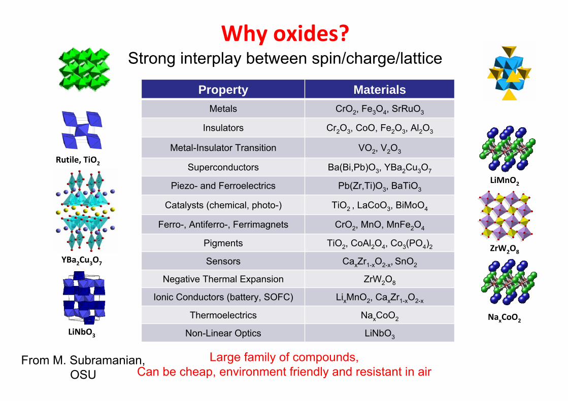
Property MaterialsMetals CrO2, Fe3O4, SrRuO3
Insulators Cr2O3, CoO, Fe2O3, Al2O3
Metal-Insulator Transition VO2, V2O3
Superconductors Ba(Bi,Pb)O3, YBa2Cu3O7
Piezo- and Ferroelectrics Pb(Zr,Ti)O3, BaTiO3
Catalysts (chemical, photo-) TiO2 , LaCoO3, BiMoO4
Ferro-, Antiferro-, Ferrimagnets CrO2, MnO, MnFe2O4
Pigments TiO2, CoAl2O4, Co3(PO4)2
Sensors CaxZr1-xO2-x, SnO2
Negative Thermal Expansion ZrW2O8
Ionic Conductors (battery, SOFC) LixMnO2, CaxZr1-xO2-x
Thermoelectrics NaxCoO2
Non-Linear Optics LiNbO3
Rutile, TiO2
YBa2Cu3O7
LiNbO3
LiMnO2
ZrW2O8
NaxCoO2
Why oxides?Strong interplay between spin/charge/lattice
Large family of compounds,Can be cheap, environment friendly and resistant in air
From M. Subramanian,OSU

PRB46, 14928 (1992)
Correlation between Seebeck / doping / Critical temperature
Introduction
High Tc superconductors
YBa2Cu3O7-

M. Ohtaki et al., JAP79, 1816 (1996)
Zn1-xAlxO (x = 0 – 0.1)Broadband model for extrinsic n type semiconductor
Large mobility of the carriers : 3 – 7cm2/Vs
= 40Wm-1K-1 at 300K=5.4 Wm-1K-1 at 1000°C
ZT = 0.3
But is too high !!!
Introduction

Metallicity (crystals) ~ 0.2 m cmLarge S S ~ +80 V/KSmall (polycrystals) Wm
(crystals) ~ 5Wm-1K-1
Na0.7CoO2‘ Phonon Glass / Electron crystal ’
I. Terasaki et al., Phys. Rev. B 56, R12685 (1997)
Na0.7CoO2P= 50 10-4 WK-2m-1
Bi2Te3P= 40 10-4 WK-2m-1
At 300K
Power factor P=S2/ at 300K
Co3+ (3d6) / Co4+ (3d5)
NaxCoO2 : Na+xCo3+
xCo4+1-xO2 Measurements on polycrystals
Introduction

High T properties of NaxCoO2
K. Fujita et al. JJAP40, 4644 (2001)
Introduction
Crystal and polycrystal measurements
Crystals : 1.5 ×1.5 × 0.03 mm3
ZT ~ 1 (for crystals only) at 800K
ZT = 1

ZT of oxides
p type :NaxCoO2, Misfit oxides
n type : TCOs
1992 1994 1996 1998 2000 2002 2004 2006 2008 20100.00.10.20.30.40.50.60.70.80.91.01.11.2
FujitaNa
xCoO
2
R. FunahashiCa
3Co
4O
9 Whisker
n-type Bulk p-type Bulk p-type single crystals
M.Ohtaki(Zn,Al,Ga)O
G. XuCa
3Co
4O
9
H. ItaharaCa
3Co
4O
9
R. FunahashiBiSrCoO
L. BoscherCa(Mn,Nb)O
3
D. BérardanGe:In
2O
3H. Kaga
ZnO-In2O
3M.Ohtaki(Zn,Al)O
M.OhtakiIn
2O
3-SnO
2
ZT
(10
00
K)
Year
2 different families for the best thermoelectric oxides• Type p : oxides related to NaxCoO2, metallic and large S
• Type n : ‘transparent conducting oxides’, degenerate semi-conductors
ZT (type p single crystals ) > ZT (type n)
Introduction

Oxides
MisfitsNaxCoO2Large S
+ metallic small p type
Model systemTexturation problems
Transparent conductors, DelafossitesLarge S, small
Large Mostly n type (some p type)
Reduction of through nanostructuration?
Semi-conductorsLarge
S, large n and p type Increase of S
through Heikes?
Introduction

Specificities of oxides

csteeNTSq Av
K. Behnia et al. JPCM 16, 5187 (2004)
Low T limit : Mott’s formula
2q5.0
Universal value for the ratio of S /
Limit T 0
)(3
/ 22
FBel ENkTC
Models
n)E(N
eTk
3S F
2B
2
FEEB
EET
ekS
))(ln(
3
22

The Heikes formula
P. M. Chaikin et al. Phys. Rev. B 13, 647 (1976)
Models
‘Simple combinatorial problem’
Calculated for organic thermoelectrics
High T limit

The Heikes formula
Te/
TeS/S
S)1()2(
The Hubbard model
S(1) , S(2) : depend on v and Q, velocity and energy operatorsValid for narrow band systems (localized correlated particles)
Limit T : S ~ entropy / carrier
for T
)x
x1ln(e
kS B
-0.4 -0.2 0.0 0.2 0.4-600
-400
-200
0
200
400
600
S(V
/K)
x
x = concentration of carriers
Holes
Electrons
P. M. Chaikin et al. Phys. Rev. B 13, 647 (1976)
Models

0.0 0.2 0.4 0.6 0.8 1.0-300-200-100
0100200300400500600
Co3+ LS + Co4+ LS : =1/2
S Hig
hT(
V/K
)x
Extra term in the Heikes formula due to the spin degeneracy
Mixed valency cation Mn+ / M(n+1)+ :
Spin entropy
1S21S2
1n
n
J. P. Doumerc JSSC 110, 419 (1994)
)xx-1ln(
ekS B
S=0 S=1/2
Models

0.0 0.2 0.4 0.6 0.8 1.0-400-300-200-100
0100200300400
(HS+LS)+HS
(HS+LS+IS)+(HS+LS+IS)
HS+HS
LS+LSLS+(HS+LS)
S HT(
V/K
)x
NaxCoO2 : Spin and orbital degeneracy Co3+ (3d6)/Co4+ (3d5)
J. P. Doumerc JSSC 109, 419 (1994)W. Koshibae et al., Phys. Rev. B 62, 6869 (2000)
)x1
xggln(
ekS
4
3B
x : Co4+ concentration
g4/g3 = 6
Large S in NaxCoO2Origin of the metallicity ?
Models

Rhombohedral crystalline field Lifting of the t2g levels degeneracy
D. J. Singh, Phys. Rev. B 61, 13397 (2000)
a1g : localized moments / heavy holese ’g : mobile carriers / light holes
FEE
22))ln((
e3k
TS
dE
d
Peak of N(EF)
S = +110V/K at 300Kcalculated for NaCo2O4
T. Yamamoto et al., Phys. Rev. B 65, 184434 (2002)
avec = N(E)<vF(E)2>
Band structure?
Metallic and large S
Models
‘Pudding mold model’ : K. Kuroki et al., JPSJ76, 083707 (2007)

M. R. Peterson et al., PRB76, 165118 (2007)M. R. Peterson et al., PRB82, 195105 (2010)
‘Thermoelectric effectsin a strongly correlated model for NaxCoO2’
t-J model : t = hopping and J = spin couplingKubo formalismValid at any T (different from the limit T →)
S = Stransport + SHeikes
Black : Heikes formulaRed : S = Stransport + SHeikes
Models
In a large part of the phase diagram (x, T, t), the Heikes formula gives a good estimate of S

Semi-conducteurs : The Heikes formula

LaCoO3
Heikes formula : possible change of sign
)x
x1ln(e
kS B
x = carrier concentration
-0.4 -0.2 0.0 0.2 0.4-600-500-400-300-200-100
0100200300400500600
S(V
/K)
x
Co4+
(3d5)Co2+
(3d7)Depending on x, S>0 or S<0
Small x |S| very large
Change of sign in LaCoO3

LaCoO3 : A site substitutionLaCoO3 x~0 : La3+Co3+O3
Sr2+ x>0 : La1-xSrx(Co3+/Co4+)O3
Ce4+ x<0 : La1-xCex(Co3+/Co2+)O3
-0.5 -0.4 -0.3 -0.2 -0.1 0.0 0.1 0.2 0.3 0.4 0.5-600-500-400-300-200-100
0100200300400500600
Co4+Co2+ x
S (
V.K
-1)
A. Maignan et al., EPJB 39, 145 (2004)
50 100 150 200 250 300 350-400
-200
0
200
400
600
800
1000
LaCoO3
Ce0.01
Sr0.02
S (
V.K
-1)
T(K)
Change of sign in LaCoO3

Formule de Heikes pour S, avec
K. Berggold et al., PRB72, 155116 (2005)
50 100 150 200 250 300 350-400
-200
0
200
400
600
800
1000
LaCoO3
Ce0.01
Sr0.02
S (
V.K
-1)
T(K)-0.5 -0.4 -0.3 -0.2 -0.1 0.0 0.1 0.2 0.3 0.4 0.5
-600-500-400-300-200-100
0100200300400500600
Co4+Co2+ x
S (
V.K
-1)
A. Maignan et al., EPJB 39, 145 (2004)
Co3+ IS
Co4+ LS
)x1
xggln(
ekS
4
3B
Spin only degeneracy
g3 = 3 / g4 = 2(experimentally 1.8)
LaCoO3
g2 = 4Cobaltites ‘112’ :A. A. Taskin et al., PRB73, 121101 (2006)

Change of sign in LaCoO3
K. Berggold et al., PRB72, 155116 (2005)
LaCoO3
Single crystals measurements

Type p : Pr1-xCaxCrO3 Orthochromites
Perovskite structure
Pr3+1-xCa2+
xCr3+/4+O3 : 3d3/3d2
S. Pal et al., Eur. Phys. J. B 53, 5 (2006)
0 100 200 300 40010-1
100
101
102
103
104
105
106
107
Pr1-xCaxCrO3
x=0.3
(
.cm
)
T(K)
x=0.05
x=0.0
Introduction of holes : Activated behavior with
a decrease of
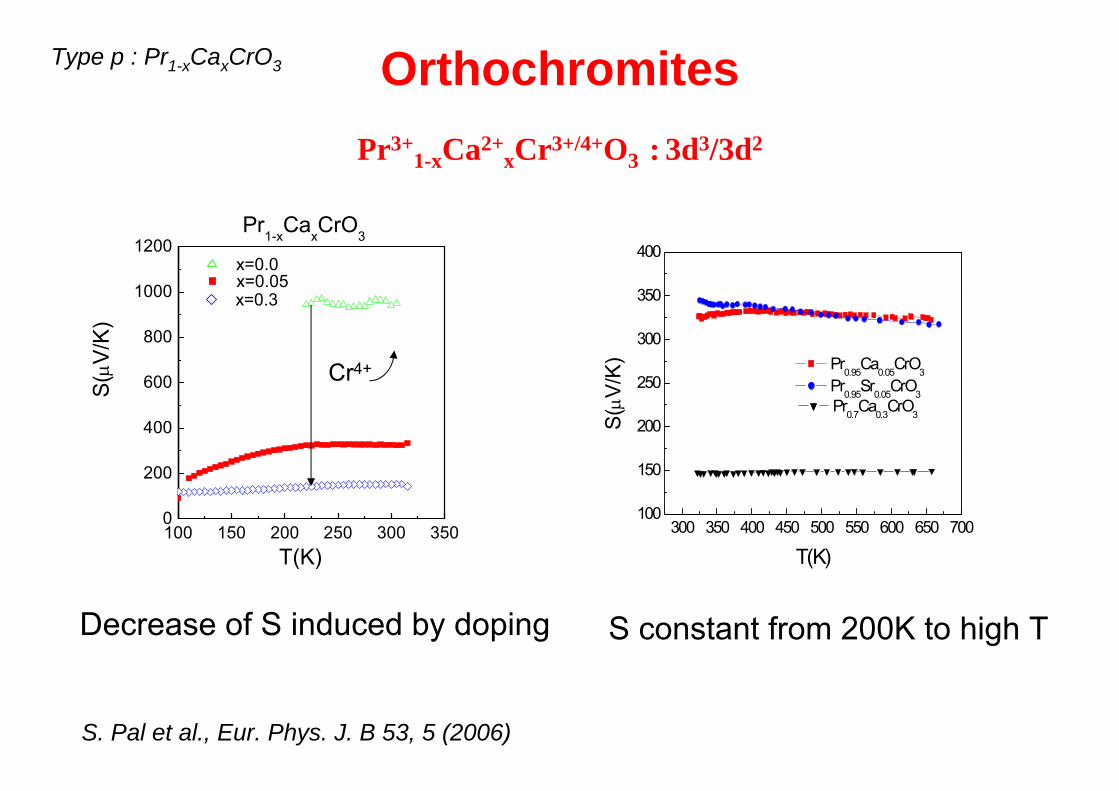
Type p : Pr1-xCaxCrO3
0
200
400
600
800
1000
1200
100 150 200 250 300 350T(K)
Pr1-xCaxCrO3
S(V
/K)
x=0.0
x=0.3
x=0.05
OrthochromitesPr3+
1-xCa2+xCr3+/4+O3 : 3d3/3d2
S. Pal et al., Eur. Phys. J. B 53, 5 (2006)
300 350 400 450 500 550 600 650 700100
150
200
250
300
350
400
Pr0.7Ca0.3CrO3
Pr0.95Ca0.05CrO3 Pr0.95Sr0.05CrO3
S(V
/K)
T(K)
Cr4+
Decrease of S induced by doping S constant from 200K to high T

0.0 0.1 0.2 0.3 0.4 0.5-100
0100200300400500600700800900
1000
x (Ca concentration)
S(
V/K
)
Pr1-xCaxCrO3 Pr1-xSrxCrO3 calculated value taking orbital degeneracy calculated value from Heikes formula
)ln(e
k)x
x1ln(ekS spinorb
BB
Marsh and Parris, Phys. Rev. B 54, 7720 (1996)
K/V9.694133ln
ek B
3d3, S = 3/2
orb=1spin = 4
3d2, S = 1
orb=3spin = 3
Type p : Pr1-xCaxCrO3
Heikes formula withspin and orbital degeneracies

Type p : Pr1-xCaxCrO3 Power factor
PF ~ 2.10-4 Wm-1K-1
Typical for oxides

Semi – conducting oxides
The Heikes formula
→ Possibility to get p and n type oxides
→ Spin and/or orbital degeneracies have to be taken into account for a quantitative analysis
→ Explains the asymmetry between n and p type
But too large resistivity !

Degenerate semi-conductors : Best n type oxides

Type n : ZnO
M. Ohtaki et al., JAP79, 1816 (1996)
Zn1-xAlxO (x = 0 – 0.1)
Broadband model for extrinsic n type semiconductor
Large mobility of the carriers : 3 – 7cm2/Vs
= 40Wm-1K-1 at 300K=5.4 Wm-1K-1 at 1000°C
ZT = 0.3
too high!

Perovskite Ca1-xSmxMnO3SrMn1-xMoxO3
Partially filled 3d levels
Mn3+ t2g3eg
1, HS JT
V(Mn)=4-x
Type n : CaMnO3

Manganese oxidesn type SrMn1-xMoxO3
0 100 200 300 400 500 600 700 80010-2
10-1
100
101
102
103
x=0
x=0.04x=0.02
(
cm)
T (K)0 100 200 300 400 500 600 700 800-500
-400
-300
-200
-100
0
x=0
x=0.02
x=0.04
S(V
/K)
T (K)
SrMnO3 : Mn4+
Mo6+ Mn3+/Mn4+
Metallic up to high T / S linear in TPower factor increases as T increases : PF = 9.10-4Wm-1K-2 for x=0.02 at 800K
Measurements by J. Hejtmanek (Prague))lnTk/3ekπS BB
2 Eσ(E)/(
3d3 t2g3 / 3d4 t2g
3eg1
J. Hejtmanek et al., PRB60, 14057 (1999)

Type n : CaMnO3 Ca0.9M0.1MnO3
M. Ohtaki et al., JSSC120, 105 (1995)
ZT ~ 0.1 à 900°C

J. L. Cohn et al., PRB72, 024422 (2006)
Type n : CaMnO3
Carrier concentration~ 1020 cm-3
Smaller mobility than in ZnO
Polarons transport in CaMnO3
Charged impurity scattering
Phonon scattering
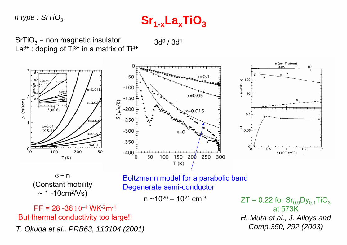
n type : SrTiO3
SrTiO3 = non magnetic insulatorLa3+ : doping of Ti3+ in a matrix of Ti4+
T. Okuda et al., PRB63, 113104 (2001)
Sr1-xLaxTiO3
PF = 28 -36 WK-2m-1
But thermal conductivity too large!!
~ n(Constant mobility
~ 1 -10cm2/Vs)
Boltzmann model for a parabolic bandDegenerate semi-conductor
ZT = 0.22 for Sr0.9Dy0.1TiO3at 573K
H. Muta et al., J. Alloys and Comp.350, 292 (2003)
n ~1020 – 1021 cm-3
3d0 / 3d1

smaller than for p type oxidesLess sensitive to correlation effects?
n type : SrTiO3 Sr1-xLaxTiO3
T. Okuda et al., PRB63, 113104 (2001)
Carrier concentration1019 -1021 cm-3

Type p : delafossites CuCr1-xMgxO2
CrO2 layers : edge shared octahedra
T. Okuda et al., PRB72, 144403 (2005), Y. Ono et al., ICT 2006
ZT = 0.04 at 950K
CuRh0.9Mg0.1O2 : ZT = 0.15 à 1000KH. Kuriyama et al., ICT2006

0 50 100 150 200 250 300 350 40010-1
100
101
102
103
104
105
x = 0.06
x = 0.03
x = 0.01
x = 0.005
x = 0.02
x = 0.00
(
.cm
)
T (K)0 50 100 150 200 250 300
0
200
400
600
800
1000
1200
x = 0.005
x = 0.01x = 0.03
x = 0.04
CuCr1-xMgxO2
x = 0.00
x = 0.06
x = 0.02
S (µ
V.K-1
)T (K)
Transport properties of CuCr1-xMgxO2
Large resistivity drop up tox=0.02
Large S drop up tox=0.02
Holes : Cr4+Activated (x=0.00) to small polaron (x>0.01)TEM/ED/EDX/XRD: xmax =0.01
Trivalent Cr S=3/2
Type p : delafossites
E. Guilmeau et al. SSC151, 1798 (2011)

10 20 30 40 50 60 70 80 90
0.0 0.1 0.2 0.30.00
0.05
0.10
0.15
0.20
In2Ge2O7
In2O3
I (a.
u.)
2
In2G
e 2O7 f
ract
ion
Nominal Ge fraction
No substitution occursor
Small Ge solubility limit
SampleIn1.9Ge0.1O3
RBragg= 2.98, Chi2=1.28
XRDIn2-xGexO3
C. Marcel et al., Active and Passive Elec. Comp., 1997, Vol. 19, pp. 217-223
D. Bérardan et al., Solid Stat. Comm. 146 (2008) 97.
Doping or microstructure effect??
SampleIn1.8Ge0.2O3
In2Ge2O7
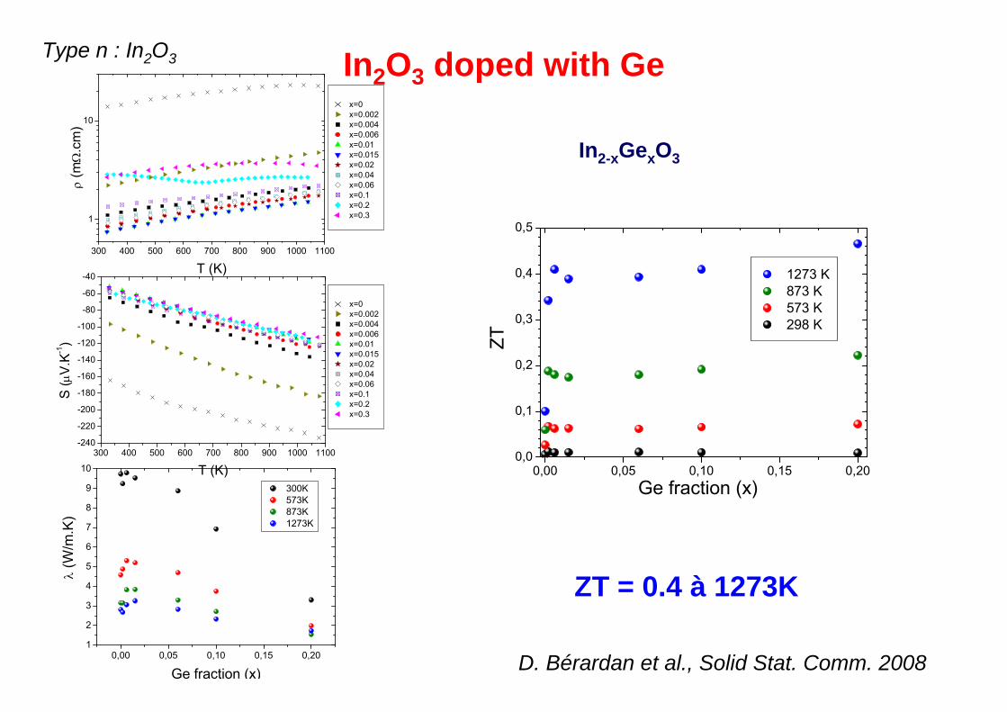
In2O3 doped with Ge
D. Bérardan et al., Solid Stat. Comm. 2008
Type n : In2O3
0,00 0,05 0,10 0,15 0,200,0
0,1
0,2
0,3
0,4
0,5
1273 K 873 K 573 K 298 K
ZTGe fraction (x)
300 400 500 600 700 800 900 1000 1100-240
-220
-200
-180
-160
-140
-120
-100
-80
-60
-40
S (
V.K-1
)
T (K)
x=0 x=0.002 x=0.004 x=0.006 x=0.01 x=0.015 x=0.02 x=0.04 x=0.06 x=0.1 x=0.2 x=0.3
300 400 500 600 700 800 900 1000 1100
1
10
(m
.c
m)
T (K)
x=0 x=0.002 x=0.004 x=0.006 x=0.01 x=0.015 x=0.02 x=0.04 x=0.06 x=0.1 x=0.2 x=0.3
0,00 0,05 0,10 0,15 0,201
2
3
4
5
6
7
8
9
10
(W
/m.K
)
Ge fraction (x)
300K 573K 873K 1273K
In2-xGexO3
ZT = 0.4 à 1273K

Degenerate semi - conductors
• Classical behavior which can be described by the Boltzmann modelSmall enhancement of the effective mass
Polaronic transport
• Mostly n type (p type in delafossites)
• Problem : too large thermal conductivityMicrostructure modification is necessary to enhance ZT

Doped CaMnO3 : New preparation techniques
Soft chemistry techniques
L. Bocher et al., Inorg. Chem. 47, 8077 (2008)
Reduction of Possible size effect?

Nb doped TiO2
Polaronic transportMeasurements for thin filmsJ. Jacimovic et al., APL102, 013901 (2013)
Search for other materials in the ‘TCO’ familyCritical role of doping through vacancies
Calculations for Cu2O (D. J. Singh et al.), …

NaxCoO2 and related metallic compounds(p type)

Cobalt bronzes family ofNaxCoO2
C. Fouassier et al., JSSC6, 532 (1973)
J. Molenda, C. Delmas, P. Dordor, A. Stoklosa, Solid Stat. Ionics 12, 473 (1989)
Na0.7CoO2-
T
S
T
NaxCoO2Misfits

Metallicity (crystals) ~ 0.2 m cmLarge S S ~ +80 V/KSmall (polycrystals) Wm
(crystals) ~ 5Wm-1K-1
Na0.7CoO2‘ Phonon Glass / Electron crystal ’
I. Terasaki et al., Phys. Rev. B 56, R12685 (1997)
Na0.7CoO2P= 50 10-4 WK-2m-1
Bi2Te3P= 40 10-4 WK-2m-1
At 300K
Power factor P=S2/ at 300K
Co3+ (3d6) / Co4+ (3d5)
NaxCoO2 : Na+xCo3+
xCo4+1-xO2 Measurements on polycrystals
Introduction

NaxCoO2KxCoO2, …
Misfits
The misfit family• n = 4 [Bi2A’2O4]RS[CoO2]b1/b2A’ = Ca2+, Sr2+ or Ba2+
• n = 3 [A’2CoO3]RS[CoO2]b1/b2A’ = Ca2+ or Sr2+
• n = 2 [Sr2O2]RS[CoO2]b1/b2[Ca2(OH)2]RS[CoO2]b1/b2
Masset et col., Phys. Rev. B 62, 166 (2000)Leligny et col., C. R. Acad. Sci. Paris, t. 2, Série II c, 409 (1999)Boullay et col., Chem. Mater. 8, 1482 (1996) Yamauchi et col., Chem. Mater. 18, 155 (2005)
CoO2 (type CdI2)
NaCl-like triple layer (RS)
a1 = a2c1 = c2 b1 b21 = 2
b2a
ab1
Heikes formula : doping influence?Band structure influence : peculiarity of CoO2 layers ?
Role of separating block layers?

Doping effect in the misfit family
21 /4v
bbCo
Ca2CoO3NaCl-like
CoO2CdI2-like
Ca3Co4O9 Electronic neutrality :[Ca2CoO3±]RS[CoO2]b1/b2
2+ 2-3+ Co 2-
>0
Modification of vCo via and b1/b2
Link between vCo and S?

0 50 100 150 200 250 30001234567
'Tl0.4SrCoO3+'
'Ca3Co4O9'
(10
-2
cm)
T(K)
Misfits
Modification of the block layersNaxCoO2Misfits
0 50 100 150 200 250 3000
20
40
60
80
100
120
140
'Tl0.4
SrCoO3+
'
'Ca3Co
4O
9'
S(V
/K)
T(K)

0 50 100 150 200 250 300
0
20
40
60
80
100
120
140
160
As-prep.
Po2
S(V
/K)
T(K)
Unique behavior of CdI2 type layers: Comparison with other oxides
Perovskite Sr2/3Y1/3CoO8/3+
Corner shared octahedraedge shared octahedra
A. Maignan et al., JSSC178, 868 (2005)
Metallicity
Seebeck 0
NaxCoO2Misfits

Influence du taux d’oxygène
Ca3Co4O9+
Co4+
0 50 100 150 200 250 3000
50
100
150
200
250
BCCOAir
BCCOAnnealed
BCCOVacuum
S(V
/K)
T(K)
M. Karppinen et al., Chem. Mater. 16, 2790 (2004)
0 100 200 300 40010-2
10-1
100
101
102
103
104
105
106
BCCOVacuum
BCCOAnnealed
BCCOAir
(
.cm
)
T(K)
S. Hébert et al.
Famille BiCaCoO, Polycristaux préparés sous air, ou en tube scellé
NaxCoO2Misfits
Co4+
Misfits : S le plus élevépour le taux de ‘Co4+’le plus faible
0 100 200 300 400
100
101
102
BSCO
BPSCO
(m
cm
)
T(K)
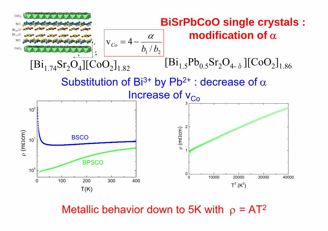
BiSrPbCoO single crystals : modification of
0 10000 20000 30000 400000
1
2
3
(m
cm
)
T2 (K2)
[Bi1.5Pb0.5Sr2O4-δ][CoO2]1.86[Bi1.74Sr2O4][CoO2]1.82
Metallic behavior down to 5K with = AT2
Substitution of Bi3+ by Pb2+ : decrease of Increase of vCo
21 /4v
bbCo

0 50 100 150 200 250 3000
20
40
60
80
100
120
BSCO
BPSCO
S(V
/K)
T(K)0 100 200 300 400
100
101
102
BSCO
BPSCO
(m
cm
)
T(K)
Increase of ‘Co4+’ associated to a decrease of S
Generalized Heikes formula : increase of vCo
3.59 for BSCO and 3.65 for BPSCO
NaxCoO2Misfits BiSrPbCoO single crystals : modification of
)x1
xggln(
ekS
4
3B

BiSrPbCoO single crystals : modification of
0 50 100 150 200 250 3000,000
0,005
0,010
0,015
BPSCO
BSCO
RH
(cm
3 /C)
T(K)
At 100K1.06 × 1021 cm-3 for BSCO 1.73 × 1021 cm-3 for BPSCO
W. Kobayashi et al., JPCM21, 235404 (2009)
t- J model : Linear T dependence of RHt ~10 – 40K
Justifies the Heikes formula?B. Kumar et al., PRB68, 104508 (2003)
Y. Wang et al., cond-mat/0305455G. Leon et al. , PRB78, 085105 (2008)
Increase of vCo3.113.18
NaxCoO2Misfits

S. Hébert et al., PSSA210, 69 (2013)
0 50 100 150 200 250 3000
2
4
6
8
10
12
14
BiBaCoO
BiSrCoO
BiCaCoO
(m
.cm
)
T(K)0 50 100 150 200 250 300
0
20
40
60
80
100
120
140
160
BiBaCoO
BiCaCoO
BiSrCoO
S (
V/K)
T(K)
0 50 100 150 200 250 3000.000
0.005
0.010
0.015
0.020
0.025
0.030
BiBaCoO
BiSrCoO
BiCaCoO
RH(c
m3 /C
)
T(K)
Influence du b1/b2
b1/b2
21Co b/b
4v
Si b1/b2 , concentration en Co4+
S à 300K dépend du taux de Co4+
modifié via le b1/b2
NaxCoO2Misfits
1.65 1.70 1.75 1.80 1.85 1.90 1.95 2.0080
90
100
110
120
130
140
150
BiBa
BiSr
BiPbCa
BiCa
S 300K
(V/
K)
b1/b2
Taux de porteurs ~ 1021 cm-3, plus élevé que pour les matériaux conventionnels
b1 : plans NaCl / b2 : plans CoO2

Heikes formula
)xx-1
ggln(
ekS
3
4B
Co valency in BiCaCoO/ BiSrCoO / BiBaCoO?
0,0 0,1 0,2 0,3 0,4 0,5 0,6 0,7 0,8 0,9 1,0-300
-200
-100
0
100
200
300
400
500
600
Spin degeneracyCo3+ S = 1/2 + Co4+ S=0 : =1/2
Heikes = 0
Spin and orbital degeneracyCo3+ LS + Co4+ LS : =1/6
S Hig
hT(
V/K)
x
3.05 -3.153.5 -3.7 for g4 / g3 = 6Hall effectHeikes (S at 300K)
NaxCoO2Misfits

Carrier concentration changes with misfit ratio b1/b210
8
6
4
2
0
10
8
6
4
2
0
single hole-like fermi surface (a1g character)
21Co b/b
4v
kF=0.57±0.05 Å-1 for BiBaCoO
similar to kF of NaxCoO2 (x=0.7)
Collaboration with
V. Brouet et al., LPS Orsay
Co3.3+ for BiBaCoO
Reliable data for vCo are obtained for BiBaCoO
Co3.2+ for BiSrCoOCo3.1+ for BiCaCoO
(=const)
V. Brouet et al., PRB76, 100403 (2007)
ARPES
NaxCoO2Misfits

Heikes formula
)x1
xggln(
ekS
4
3B
g3 / g4 = 1/2 instead of 1/6 Confirms the results in BiCaCoO : vCo = 3.24
M. Pollet et al., JAP101, 083708 (2007)
0,0 0,1 0,2 0,3 0,4 0,5 0,6 0,7 0,8 0,9 1,0-300
-200
-100
0
100
200
300
400
500
600
Spin degeneracyCo3+ S = 1/2 + Co4+ S=0 : =1/2
Heikes = 0
Spin and orbital degeneracyCo3+ LS + Co4+ LS : =1/6
S Hig
hT(
V/K)
x
NaxCoO2Misfits
Valence du Co dans la famille BiCaCoO/ BiSrCoO / BiBaCoO
3.24M. Pollet et al.,
JAP101, 083708 (2007)
3.1 -3.3J. Bobroff et al., PRB76, 100407
(2007)
3.3V. Brouet et al.,PRB76, 100403
(2007)
3.05 -3.15W. Kobayashi et al.
3.33P. Limelette et al., PRL97, 046601
(2006)
3.5 -3.7
SusceptibilitéBiCaCoO
RMNARPESBiBaCoO
Effet HallSeebeck avec S(H)g3/g4 = 1BiCaCoO
Heikesg3/g4 = 1/6S à 300K
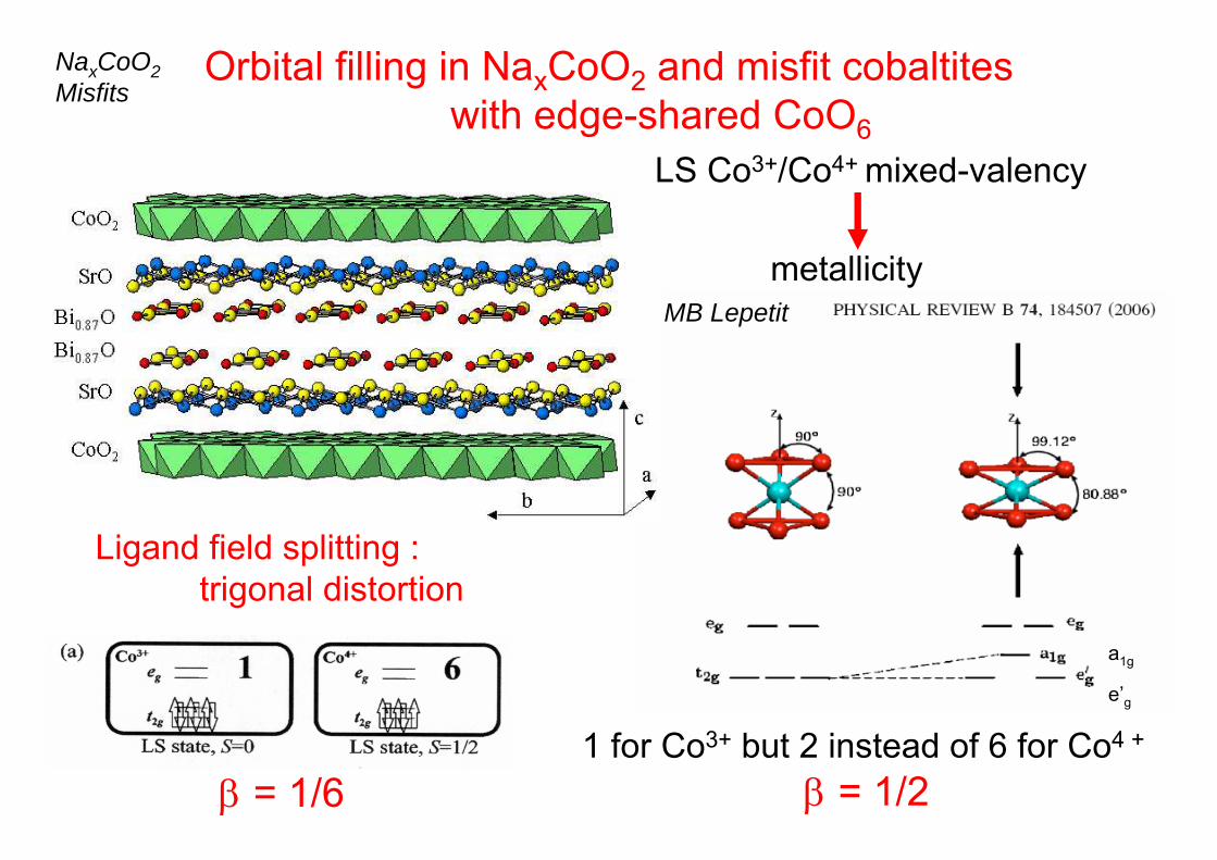
Orbital filling in NaxCoO2 and misfit cobaltiteswith edge-shared CoO6
Ligand field splitting :trigonal distortion
MB Lepetit
LS Co3+/Co4+ mixed-valency
metallicity
a1g
e’g
= 1/61 for Co3+ but 2 instead of 6 for Co4 +
= 1/2
NaxCoO2Misfits

NaxCoO2Misfits
Importance des corrélations électroniques
P. Limelette, PRB71, 233108 (2005)
csteeNTSq Av
Pour T→0
P. Limelette, PRL97, 046601 (2006)
S ~ T

Low T : Spin entropy
BiCaCoO : excess of S at low TA. Maignan et al., JPCM 15, 2711 (2003)
Observed also in NaxCoO2[Wang et al. Nature 423, 425 (2003)]
NaxCoO2Misfits

Scaling MR et MTEPLien avec la susceptibilité
Spin entropy at low TMisfit BiCaCoO
Na0.7CoO2
A. Maignan et al., JPCM15, 2711 (2003)
Y. Wang et al., Nature423, 425 (2003)
Scaling law for S(H) : paramagnetic spins S=1/2Brillouin function
P. Limelette et al., PRL97, 046601 (2006)
Decrease of S under field at low TDue to the alignement of paramagnetic spins
Peak of susceptibilityJ. Bobroff et al.,
PRB76, 100407 (2007)

Misfits
CoO2 (type CdI2)
NaCl-like triple layer (RS)
Co3+ (3d6) / Co4+ (3d5)Low spin : t2g orbitals+ triangular network
0 50 100 150 200 250 300100
101
102
103
104
BiBaCoOBiSrCoO
BiCaCoO
(m
.cm
)
T(K)
0 50 100 150 200 250 3000
20
40
60
80
100
120
140
160
BiBaCoO
BiCaCoO
BiSrCoO
S (
V/K)
T(K)
For T > 100K : metallicity + large S
• High T : Seebeck depends on Co4+
Heikes formula with spin / orbital degeneracy
• Low T : electronic correlations : S ~ T+ spin entropy depending on doping
• High T limit : small t from Hall effect. Justifies the Heikes formula?
S. Hébert et al., PRB64, 172101 (2001), P. Limelette et al., PRL97, 046601 (2006), W. Kobayashi et al., JPCM21, 235404 (2009)
Misfit oxidesNaxCoO2Misfits

0 50 100 150 200 250 3000
20406080
100120140160
S(V
/K)
T(K)
Thermoelectric power of misfits
Spin entropy (depending on doping)Electronic correlations : S ~ T
High T Seebeck, depends on Co4+
(Heikes formula with = 1/2)
BiCaCoO

Power factor
0 100 200 3000
1
2
3
4
Temperature (K)
Pow
er F
acto
r (W
/cm
K2 )
BiSrCoO
BiPbSrCoO
BiBaCoO
BiCaCoO
enhancement for BiBaCoO and BiPbSrCoO
P is almost independent of carrier concentration
In conventional semiconducting thermoelectric material such as Bi2Te3, n is an important parameter to tune the properties.
How to modify the electronic properties?Influence of the block layer?
2.10-4 Wm-1K-2 at 300K
NaxCoO2Misfits

Role of the block layer?
• Role of Na+ : Curie-Weiss behavior obtained by introducing theelectrostatic potential of Na+ (Co3+ S = 0 / Co4+ S = 1/2)C. Marianetti et al., PRL98, 176405 (2007)
•Kagomé lattice in NaxCoO2 with x = 2/3 : strong electronic correlationsF. Lechermann et al., PRL107, 236404 (2011)
Curie-Weiss
NaxCoO2Misfits

NaxCoO2Misfits Thermal conductivity
Measurements of single crystals (Harman method)
A. Satake et al., JAP96, 931 (2004)
smaller in misfits
Influence of incommensurability?
• Charge transfer between the layers : S300K mostly depends on the ratio Co3+/Co4+
• Low T : electronic correlations influence (S ~ T) + S(H) term
• Small
Power factor is constant : modification of the block layers? Influence on thermal conductivity?
NaxCoO2Misfits Conclusion

Seebeck coefficient : Major role of the spin and orbital term
Importance of electronic correlations
Conclusion
• n type oxides : degenerate semi-conductorsSeebeck described in a first approach by Mott’s formula
Polaronic transport
• p type oxides
)xx-1ln(
ekS B
ZT (n type) < ZT (p type)Thermal conductivity : mostly coming from the lattice

How to enhance ZT??
Investigation of thermal conductivityMicrostructures to reduce thermal conductivity
Low dimensional structuresNanostructuration and electronic correlations?
Investigation of new families (pb of stability!) Anionic subsitutions (oxyselenides)

2DEG SrTiO3
Nanostructuration :Increase of S
2D electron gas in SrTiO3H. Ohta et al., Nat. Mater. 6, 129 (2007)
‘ZT’ = 2.4!
of SrTiO3 single crystals
SrTi1-xNbxO3

NaxCoO2 nanowires
Sol-gel electrospinning
F. Ma et al., J. Phys. Chem. C 114, 22038 (2010)
~ .m?Resistivityoverestimated by 3 orders ofmagnitude by themeasurementtechnique?
Same technique as for Ca3Co4O9
Lin et al., J. Phys. Chem. C 114, 10061
(2010)
Nanostructuration

Substitution anionique : BiSrCuSeO
L. D. Zhao et al., APL97, 092118 (2010)
Augmentation de la covalence
Augmentation de la conductivité électrique Dopage par des trous dans les couches (Bi2O2)2+
via la substitution de Sr2+ par Bi3+

L. Yong et al., JACS133, 20112 (2011)
Influence d’un déficit en Cu
Cu deficiency in the (Cu2Se2)2- layer

Collaborators
Laboratoire CRISMATWataru Kobayashi (Tsukuba), Hidefumi Takahashi (Nagoya),
Ramzy Daou, Raymond Frésard, Emmanuel Guilmeau, Antoine Maignan, Christine Martin,
Denis Pelloquin, Olivier Perez
Patrice Limelette, GREMAN, ToursJulien Bobroff, Véronique Brouet, LPS, Orsay

+ Low thermal conductivity
Extremely reduced samples to get better conductivityStability?
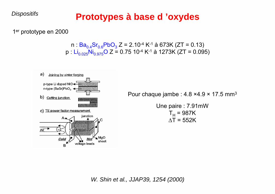
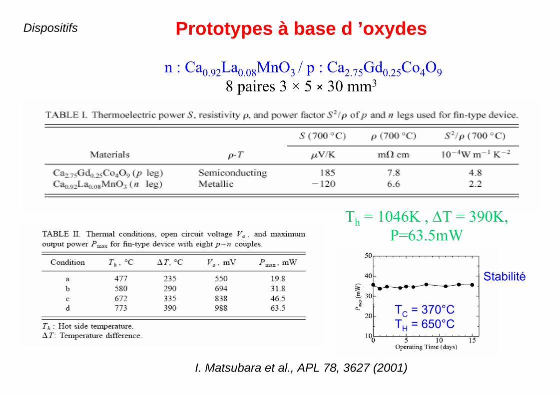
Dispositifs Prototypes à base d ’oxydes
W. Shin et al., JJAP39, 1254 (2000)
n : Ba0.4Sr0.6PbO3 Z = 2.10-4 K-1 à 673K (ZT = 0.13)p : Li0.025Ni0.975O Z = 0.75 10-4 K-1 à 1273K (ZT = 0.095)
Pour chaque jambe : 4.8 ×4.9 × 17.5 mm3
Une paire : 7.91mWTH = 987KT = 552K
1er prototype en 2000
Prototypes à base d ’oxydes
I. Matsubara et al., APL 78, 3627 (2001)
n : Ca0.92La0.08MnO3 / p : Ca2.75Gd0.25Co4O98 paires 3 × 5 × 30 mm3
Th = 1046K , T = 390K, P=63.5mW
Dispositifs
TC = 370°CTH = 650°C
Stabilité

Dispositifs La0.9Bi0.1NiO3 / Ca2.7Bi0.3Co4O9
R. Funahashi et al., APL 85, 1036 (2004)R. Funahashi et al., JAP99, 066117 (2006)
n : La0.9Bi0.1NiO3 / p : Ca2.7Bi0.3Co4O91 jonction : TH = 1073K, T = 500K, P = 94mW
140 pairesTH = 1072K, T = 551K
Chargeur pour téléphone portableTH = 1072K!

Dispositifs Ca3Co4O9/Ca0.95Sm0.05MnO3
TH = 1025K, T = 925K, P = 31.5mW4 × 4 × 5 ou10 mm3
2 paires
E. Sudhakar Reddy et al., J. Phys. D Appl. Phys. 38, 3751 (2005)
Prototype ‘unileg’Un seul matériau (ici type n)
Choix du matériau avec le meilleur ZTDiminution des contraintes mécaniques
C. Goupil, S. Lemonnier et al.

Dispositifs
0.150.0162NCa0.95Sm0.05MnO3/ Ca0.95Sm0.05MnO3
Present work
0.570.0312PNCa3Co4O9 / Ca0.95Sm0.05MnO3Sudhakar et al.
0.820.0898PN(Gd) Ca3Co4O9 / (La) CaMnO3Matsubara et al.
0.30.0342PN(Li) NiO / (Ba, Sr) PbO3Shin et al.
0.150.031PNCa2.7Bi0.3Co4O9 / La0.9Bi0.1NiO3Funahashi et al.
MFPower (W)Nb CoupleTypeMaterialsName
Comparaison des modules
Manufacturing factorMF = Rideal / Rint,
S. Lemonnier, C. Goupil et al.
Optimisation des contacts nécessaire!

Type n : SrTiO3 dopé au La450mW/cm2 pour T = 360K
Modules et prototypesDispositifs