synchronous oeic integrating receiver for optically
TRANSCRIPT
sensors
Article
Synchronous OEIC Integrating Receiver forOptically Reconfigurable Gate Arrays
Carlos Sánchez-Azqueta 1,2,*, Bernhard Goll 1, Santiago Celma 2 and Horst Zimmermann 1
1 Institute of Electrodynamics, Microwave and Circuit Engineering, Vienna University of Technology,Gußhausstraße 25/354, Vienna 1040, Austria; [email protected] (B.G.);[email protected] (H.Z.)
2 Group of Electronic Design, Aragón Institute of Engineering Research, Universidad de Zaragoza,Pedro Cerbuna 12, Zaragoza 50009, Spain; [email protected]
* Correspondence: [email protected]; Tel.: +34-876-553-547
Academic Editor: Vittorio M. N. PassaroReceived: 28 April 2016; Accepted: 20 May 2016; Published: 25 May 2016
Abstract: A monolithically integrated optoelectronic receiver with a low-capacitance on-chip pinphotodiode is presented. The receiver is fabricated in a 0.35 µm opto-CMOS process fed at 3.3 V anddue to the highly effective integrated pin photodiode it operates at µW. A regenerative latch acting asa sense amplifier leads in addition to a low electrical power consumption. At 400 Mbit/s, sensitivitiesof −26.0 dBm and −25.5 dBm are achieved, respectively, for λ = 635 nm and λ = 675 nm (BER = 10−9 )with an energy efficiency of 2 pJ/bit.
Keywords: integrated optoelectronics; integrated pin photodiode; integrating receiver
1. Introduction
Field programmable gate arrays (FPGAs) require reconfiguration times of several milliseconds [1],which makes them unsuitable for applications demanding high-speed reconfiguration capabilities.For such applications, alternative solutions such as multi-context FPGAs, digital application processorswith distributed network architectures (DAPs/DNAs) or dynamic reconfigurable processors (DRPs)have been developed, whose operation is based on incorporating several reconfiguration contexts inspecific memory banks. Such solutions achieve reconfiguration speeds in the range of hundreds ofmegahertz but at the cost of a very low gate density.
To address this issue, holographic memories in conjunction with optically reconfigurable gatearrays (ORGAs) are proposed as a viable solution for applications demanding high reconfigurationspeeds and gate densities [1,2]. The reconfiguration contexts are stored in the whole 3-D volumeof the holographic memory in a page structure, thus achieving high density, and they are retrievedprojecting the information stored in each page on an array of optical detectors, which allows operationat hundreds of megahertz [1,2].
The optical detectors in charge of retrieving the information stored in the holographic memoryneed to satisfy stringent requirements in terms of sensitivity, integration density and low power. As aconsequence, solutions based on conventional optical detectors with a transimpedance amplifier (TIA)are not feasible due to their large area and compromise between power consumption and performance.For example, [3] achieves good energy efficiency at 1 pJ/bit but at an input optical average power of−1.7 dBm and in a very expensive 32 nm silicon on insulator (SOI) CMOS process; more recently, anoptical detector at 2.7 pJ/bit in 65 nm has been reported [4], but requiring −4.9 dBm average opticalpower. In contrast, [5] operates at a reduced −31.8 dBm input optical power but with 55 pJ/bit energyefficiency and using a high-voltage avalanche photodiode (PD).
Sensors 2016, 16, 761; doi:10.3390/s16060761 www.mdpi.com/journal/sensors
Sensors 2016, 16, 761 2 of 6
An alternative to TIA-based optical receivers that is gaining attention for communicationsapplications with a tight power budget is the integrating optical receiver. Already introduced foroptical memories [6] or highly parallel optical interconnects [7], it mainly uses digital circuitry, whichresults in a drastic reduction in power consumption and makes it compatible with process scaling toachieve higher data rates. Recently reported implementations achieve Gbit/s with energy efficienciesof 0.9 pJ/bit [8] and 4.5 pJ/bit [9]. In [8] a multi-quantum well (MQW) pin PD was flip-chip bondedto a CMOS chip and in [9] an electroabsorption modulator at 1550 nm was used. However, the maindisadvantage of integrating optical receivers is their reduced sensitivity, which is reported to be−16.5 dBm at 1 Gbit/s in [8], and −19.4 dBm at 1.2 Gbit/s in [9].
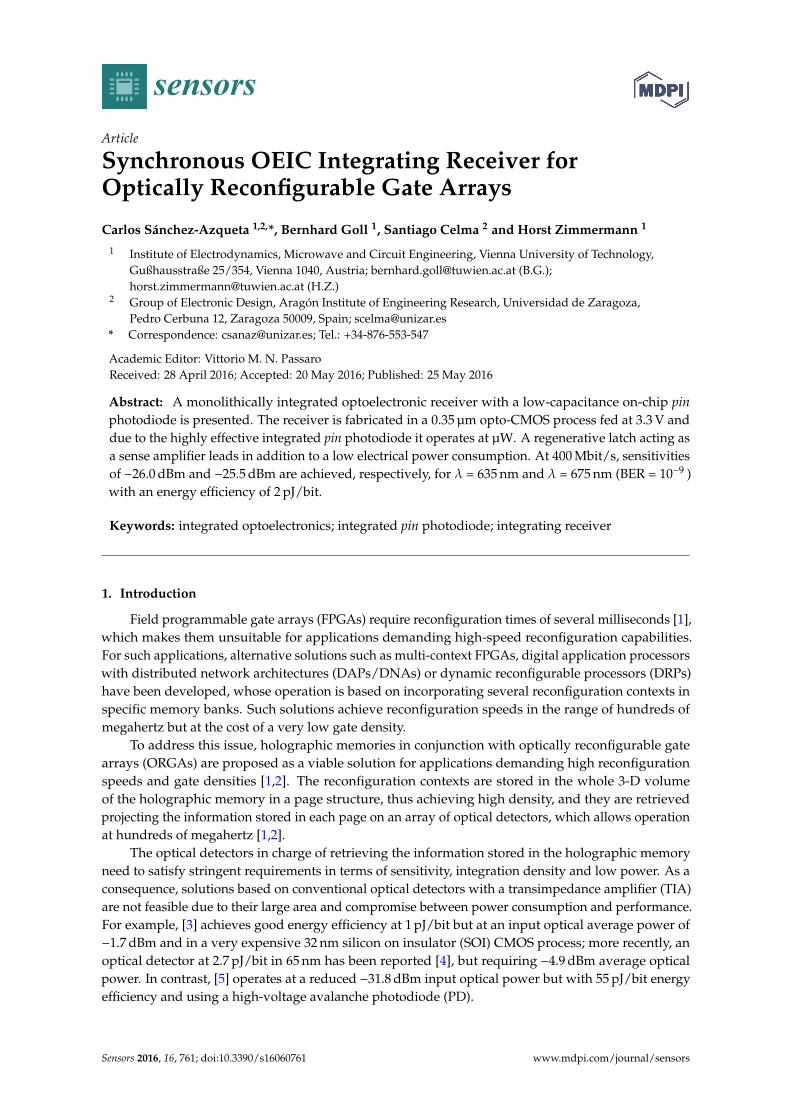
In an integrating optical receiver, the voltage that is generated by the photocurrent across thePD’s capacitance, and therefore its photo-sensitivity, is inversely proportional to the capacitancevalue. For this reason, highly sensitive integrating receivers can be implemented by their monolithicintegration into an opto-electronic integrated circuit (OEIC) along with the PD. Standard silicon CMOSand BiCMOS technologies allow the integration of small-area pin PDs that feature a responsivity higherthan 0.5 A W−1 and a −3 dB cut-off frequency above 1 GHz with a parasitic capacitance lower than100 fF [10]. A cross-section of the fabricated pin photodiode with anti-reflective coating (ARC) layer isshown in Figure 1. Its bandwidth exceeds 500 MHz already for a reverse bias of −2 V at 675 nm [11].The low doped (a few 1013 cm−3), 15 µm thick epitaxial p- layer is responsible for the high bandwidthand the low capacitance of the integrated pin photodiode, whereas the ARC layer and the opticalwindow contribute to enhance its responsivity, which would drop by 19 % at 650 nm if they werenot present.
Figure 1. Cross-section of the integrated pin photodiode with anti-reflective coating (ARC) layer andlow-doped, 15 µm thick epitaxial p- layer.
This paper presents a monolithic integrating optical receiver with a highly efficient 50 µm pin PDfeaturing 50 fF capacitance. The circuit is implemented in a 0.35 µm opto-CMOS process fed at 3.3 Vand it achieves 400 Mbit/s with a bit error ratio (BER) better than 10−9 for an average input opticalpower of −26 dBm. The regenerative latch consumes 790 µW, which yields an energy efficiency of2 pJ/bit, and, along with the output buffer (excluding the PDs) occupies 50 µm × 30 µm.
2. OEIC Architecture and Operation
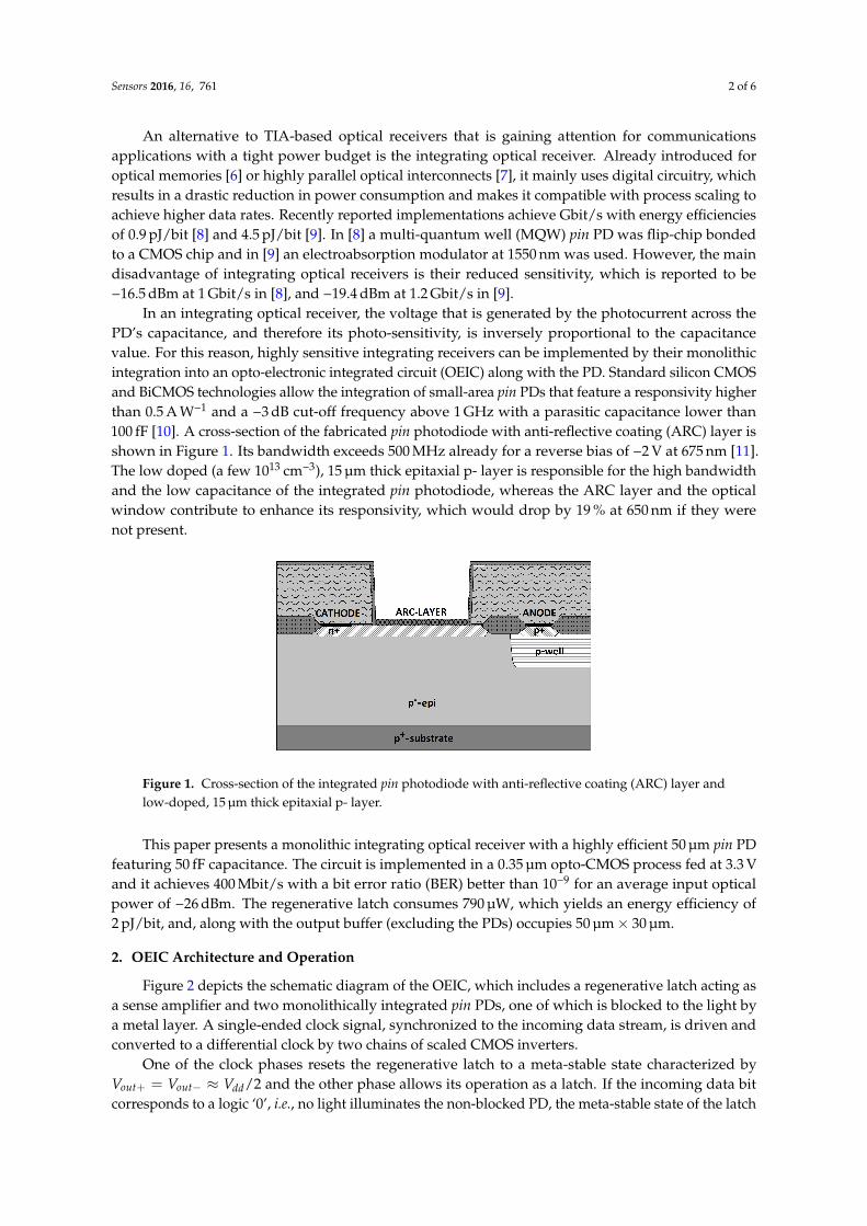
Figure 2 depicts the schematic diagram of the OEIC, which includes a regenerative latch acting asa sense amplifier and two monolithically integrated pin PDs, one of which is blocked to the light bya metal layer. A single-ended clock signal, synchronized to the incoming data stream, is driven andconverted to a differential clock by two chains of scaled CMOS inverters.
One of the clock phases resets the regenerative latch to a meta-stable state characterized byVout+ = Vout− ≈ Vdd/2 and the other phase allows its operation as a latch. If the incoming data bitcorresponds to a logic ‘0’, i.e., no light illuminates the non-blocked PD, the meta-stable state of the latch
Sensors 2016, 16, 761 3 of 6
is broken by a compensation current (Figure 2) discharging the capacitance of the blocked PD, whichdrives the latch reliably to the stable state (out− to ‘1’ and out+ to ‘0’, note the inverting behaviourof the buffers). In turn, if the incoming data bit corresponds to a logic ‘1’, i.e., the non-blocked PD isilluminated, the photocurrent generated within discharges its capacitance and drives the latch to theother stable state (out− to ‘0’ and out+ to ‘1’).
Figure 2. Circuit diagram of the opto-electronic integrated circuit (OEIC). The two clock phases(clk+ and clk−) successively activate and deactivate the latch.
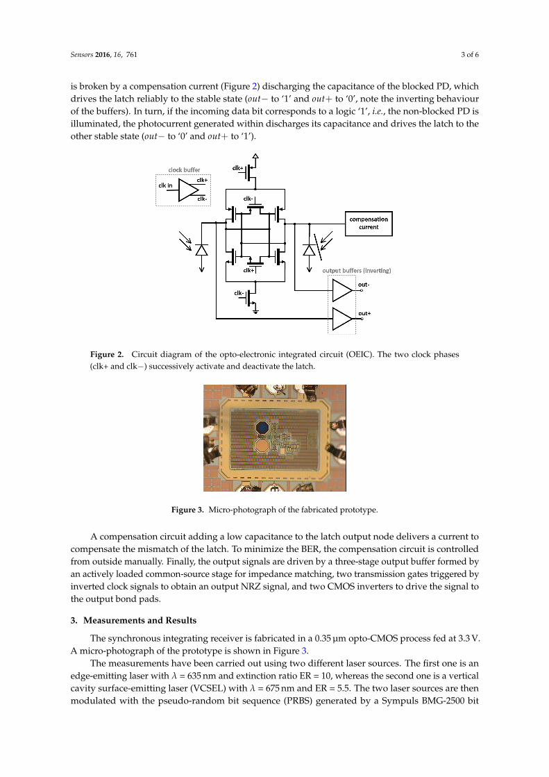
Figure 3. Micro-photograph of the fabricated prototype.
A compensation circuit adding a low capacitance to the latch output node delivers a current tocompensate the mismatch of the latch. To minimize the BER, the compensation circuit is controlledfrom outside manually. Finally, the output signals are driven by a three-stage output buffer formed byan actively loaded common-source stage for impedance matching, two transmission gates triggered byinverted clock signals to obtain an output NRZ signal, and two CMOS inverters to drive the signal tothe output bond pads.
3. Measurements and Results
The synchronous integrating receiver is fabricated in a 0.35 µm opto-CMOS process fed at 3.3 V.A micro-photograph of the prototype is shown in Figure 3.
The measurements have been carried out using two different laser sources. The first one is anedge-emitting laser with λ = 635 nm and extinction ratio ER = 10, whereas the second one is a verticalcavity surface-emitting laser (VCSEL) with λ = 675 nm and ER = 5.5. The two laser sources are thenmodulated with the pseudo-random bit sequence (PRBS) generated by a Sympuls BMG-2500 bit
Sensors 2016, 16, 761 4 of 6
pattern generator, and the average power of the modulated light signal is controlled by an opticalattenuator before it is fed into the OEIC receiver by a multi-mode optical fiber.
A twin-output internally synchronized Agilent 81134A generator is used to provide separatedclock signals for the bit pattern generator and the OEIC receiver with tuneable delay. For themeasurement of the recovered signal, a Picoprobe 34A on-wafer active probe with 0.1 pF parallel10 MΩ input impedance and an attenuation of 1:20 is used to deliver the signal to a 2 GHz bandwidthLeCroy WaveRunner 204Xi oscilloscope for eye diagram measurements, and to a Sympuls SBF-10Gbit error analyser via a MiniCircuits ZFL-1000LN+ amplifier to obtain BER information. Finally, theaverage power of the modulated light signal is measured directly by the reading of the current flowingthrough the substrate of the OEIC (the anode of the integrated pin PD is formed by the p+ substrateand all transistors are isolated from the substrate by deep n-wells or n-wells), taking into account thesensitivity of the PD, which is 0.51 A W−1 for 635 nm and 0.53 A W−1 for 675 nm.
−29 −28 −27 −26 −2510
−10
10−8
10−6
10−4
10−2
BE
R
average optical power (dBm)
400 Mb/s, λ=635 nm
350 Mb/s, λ=635 nm
400 Mb/s, λ=675 nm
350 Mb/s, λ=675 nm
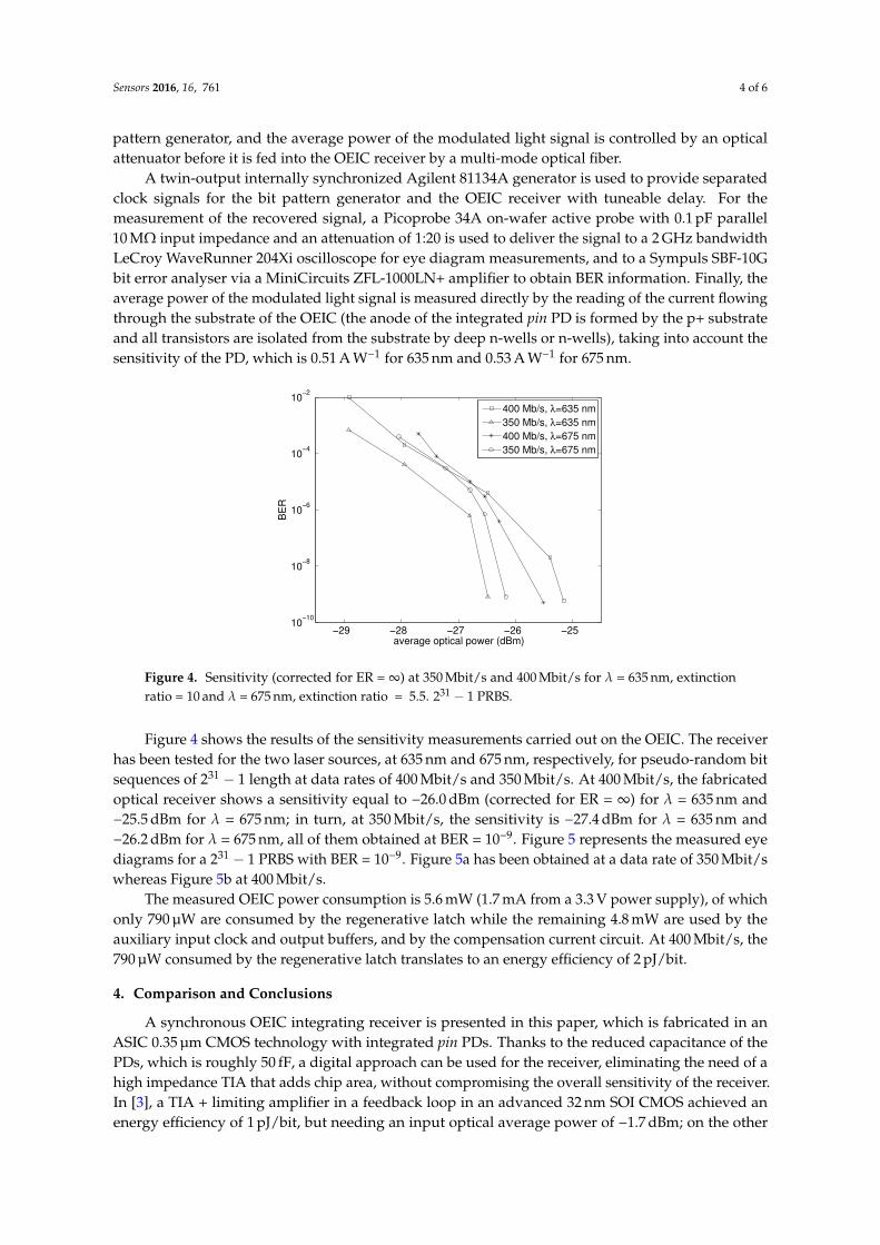
Figure 4. Sensitivity (corrected for ER = ∞) at 350 Mbit/s and 400 Mbit/s for λ = 635 nm, extinctionratio = 10 and λ = 675 nm, extinction ratio = 5.5. 231 − 1 PRBS.
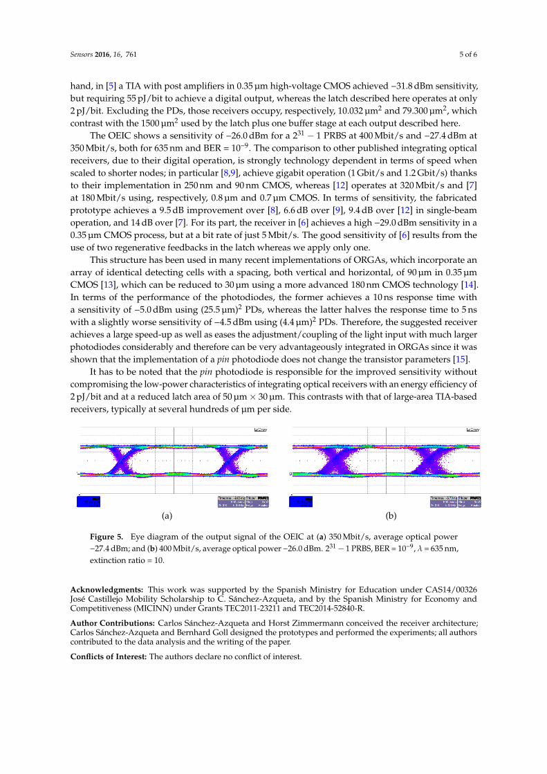
Figure 4 shows the results of the sensitivity measurements carried out on the OEIC. The receiverhas been tested for the two laser sources, at 635 nm and 675 nm, respectively, for pseudo-random bitsequences of 231 − 1 length at data rates of 400 Mbit/s and 350 Mbit/s. At 400 Mbit/s, the fabricatedoptical receiver shows a sensitivity equal to −26.0 dBm (corrected for ER = ∞) for λ = 635 nm and−25.5 dBm for λ = 675 nm; in turn, at 350 Mbit/s, the sensitivity is −27.4 dBm for λ = 635 nm and−26.2 dBm for λ = 675 nm, all of them obtained at BER = 10−9. Figure 5 represents the measured eyediagrams for a 231 − 1 PRBS with BER = 10−9. Figure 5a has been obtained at a data rate of 350 Mbit/swhereas Figure 5b at 400 Mbit/s.
The measured OEIC power consumption is 5.6 mW (1.7 mA from a 3.3 V power supply), of whichonly 790 µW are consumed by the regenerative latch while the remaining 4.8 mW are used by theauxiliary input clock and output buffers, and by the compensation current circuit. At 400 Mbit/s, the790 µW consumed by the regenerative latch translates to an energy efficiency of 2 pJ/bit.
4. Comparison and Conclusions
A synchronous OEIC integrating receiver is presented in this paper, which is fabricated in anASIC 0.35 µm CMOS technology with integrated pin PDs. Thanks to the reduced capacitance of thePDs, which is roughly 50 fF, a digital approach can be used for the receiver, eliminating the need of ahigh impedance TIA that adds chip area, without compromising the overall sensitivity of the receiver.In [3], a TIA + limiting amplifier in a feedback loop in an advanced 32 nm SOI CMOS achieved anenergy efficiency of 1 pJ/bit, but needing an input optical average power of −1.7 dBm; on the other
Sensors 2016, 16, 761 5 of 6
hand, in [5] a TIA with post amplifiers in 0.35 µm high-voltage CMOS achieved −31.8 dBm sensitivity,but requiring 55 pJ/bit to achieve a digital output, whereas the latch described here operates at only2 pJ/bit. Excluding the PDs, those receivers occupy, respectively, 10.032 µm2 and 79.300 µm2, whichcontrast with the 1500 µm2 used by the latch plus one buffer stage at each output described here.
The OEIC shows a sensitivity of −26.0 dBm for a 231 − 1 PRBS at 400 Mbit/s and −27.4 dBm at350 Mbit/s, both for 635 nm and BER = 10−9. The comparison to other published integrating opticalreceivers, due to their digital operation, is strongly technology dependent in terms of speed whenscaled to shorter nodes; in particular [8,9], achieve gigabit operation (1 Gbit/s and 1.2 Gbit/s) thanksto their implementation in 250 nm and 90 nm CMOS, whereas [12] operates at 320 Mbit/s and [7]at 180 Mbit/s using, respectively, 0.8 µm and 0.7 µm CMOS. In terms of sensitivity, the fabricatedprototype achieves a 9.5 dB improvement over [8], 6.6 dB over [9], 9.4 dB over [12] in single-beamoperation, and 14 dB over [7]. For its part, the receiver in [6] achieves a high −29.0 dBm sensitivity in a0.35 µm CMOS process, but at a bit rate of just 5 Mbit/s. The good sensitivity of [6] results from theuse of two regenerative feedbacks in the latch whereas we apply only one.
This structure has been used in many recent implementations of ORGAs, which incorporate anarray of identical detecting cells with a spacing, both vertical and horizontal, of 90 µm in 0.35 µmCMOS [13], which can be reduced to 30 µm using a more advanced 180 nm CMOS technology [14].In terms of the performance of the photodiodes, the former achieves a 10 ns response time witha sensitivity of −5.0 dBm using (25.5 µm)2 PDs, whereas the latter halves the response time to 5 nswith a slightly worse sensitivity of −4.5 dBm using (4.4 µm)2 PDs. Therefore, the suggested receiverachieves a large speed-up as well as eases the adjustment/coupling of the light input with much largerphotodiodes considerably and therefore can be very advantageously integrated in ORGAs since it wasshown that the implementation of a pin photodiode does not change the transistor parameters [15].
It has to be noted that the pin photodiode is responsible for the improved sensitivity withoutcompromising the low-power characteristics of integrating optical receivers with an energy efficiency of2 pJ/bit and at a reduced latch area of 50 µm × 30 µm. This contrasts with that of large-area TIA-basedreceivers, typically at several hundreds of µm per side.
(a) (b)
Figure 5. Eye diagram of the output signal of the OEIC at (a) 350 Mbit/s, average optical power−27.4 dBm; and (b) 400 Mbit/s, average optical power −26.0 dBm. 231 − 1 PRBS, BER = 10−9, λ = 635 nm,extinction ratio = 10.
Acknowledgments: This work was supported by the Spanish Ministry for Education under CAS14/00326José Castillejo Mobility Scholarship to C. Sánchez-Azqueta, and by the Spanish Ministry for Economy andCompetitiveness (MICINN) under Grants TEC2011-23211 and TEC2014-52840-R.
Author Contributions: Carlos Sánchez-Azqueta and Horst Zimmermann conceived the receiver architecture;Carlos Sánchez-Azqueta and Bernhard Goll designed the prototypes and performed the experiments; all authorscontributed to the data analysis and the writing of the paper.
Conflicts of Interest: The authors declare no conflict of interest.

Sensors 2016, 16, 761 6 of 6
References
1. Watanabe, M.; Fujime, R.; Kobayashi, F. A Dynamic Differential Reconfiguration Circuit for OpticallyDifferential Reconfigurable Gate Arrays. In Proceedings of the 2006 49th IEEE International MidwestSymposium on Circuits and Systems, San Juan, Puerto Rico, 6–9 August 2006; pp. 94–98.
2. Kim, B.; Lee, J. 2-D non-isolated pixel 6/8 modulation code. IEEE Trans. Magn. 2014, 50, 1–4.3. Proesel, J.E.; Lee, B.G.; Baks, C.W.; Schow, C.L. 35-Gb/s VCSEL-Based Optical Link Using 32-nm SOI CMOS
Circuits. In Proceedings of the Optical Fiber Communication Conference and Exposition and the NationalFiber Optic Engineers Conference (OFC/NFOEC), Anaheim, CA, USA, 17–21 March 2013; pp. 1–3.
4. Pan, Q.; Hou, Z.; Wang, Y.; Lu, Y.; Ki, W.-H.; Wang, K.C.; Yue, C.P. A 48-mW 18-Gb/s Fully Integrated CMOSOptical Receiver with Photodetector and Adaptive Equalizer. In Proceedings of the 2014 Symposium onVLSI Circuits Digest of Technical Papers, Honolulu, HI, USA, 10–13 June 2014; pp. 1–2.
5. Brandl, P.; Enne, R.; Jukic, T.; Zimmermann, H. Monolithically integrated optical receiver with large-areaavalanche photodiode in high-voltage CMOS technology. Electron. Lett. 2014, 50, 1541–1543.
6. Schaffer, T.; Mitkas, P. Smart photodetector array for page-oriented optical memory in 0.35-µm CMOS.IEEE Photonics Technol. Lett. 1998, 10, 866–868.
7. Ayadi, K.; Kuijk, M.; Heremans, P.; Bickel, G.; Borghs, G.; Vounckx, R. A monolithic optoelectronic receiverin standard 0.7-µm CMOS operating at 180 MHz and 176-fJ light input energy. IEEE Photonics Technol. Lett.1997, 9, 88–90.
8. Emami-Neyestanak, A.; Palermo, S.; Lee, H.C.; Horowitz, M. CMOS Transceiver with Baud Rate ClockRecovery for Optical Interconnects. In Proceedings of the 2004 Symposium on VLSI Circuits Digest ofTechnical Papers, Honolulu, HI, USA, 17–19 June 2004; pp. 410–413.
9. Roth, J.; Palermo, S.; Helman, N.; Bour, D.; Miller, D.; Horowitz, M. An optical interconnect transceiver at1550 nm using low-voltage electroabsorption modulators directly integrated to CMOS. J. Lightw. Technol.2007, 25, 3739–3747.
10. Brandl, P.; Zimmermann, H. 3 Gbit/s optical receiver IC with high sensitivity and large integrated pinphotodiode. Electron. Lett. 2013, 49, 552–554.
11. Brandl, P.; Schidl, S.; Zimmermann, H. PIN Photodiode Optoelectronic Integrated Receiver Used for 3-Gb/sFree-Space Optical Communication. IEEE J. Sel. Top. Quantum Electron. 2014, 20, 391–400.
12. Woodward, T.K.; Krishnamoorthy, A.V.; Goossen, K.W.; Walker, J.A.; Cunningham, J.E.; Jan, W.Y.;Chirovsky, L.M.F.; Hui, S.P.; Tseng, B.; Kossives, D.; et al. Clocked-sense-amplifier-based smart-pixeloptical receivers. IEEE Photonics Technol. Lett. 1996, 8, 1067–1069.
13. Ito, H.; Watanabe, M. Mono-Instruction Set Computer Architecture on a 3D Optically Reconfigurable GateArray. In Proceedings of the 2013 IEEE Electrical Design of Advanced Packaging Systems Symposium(EDAPS), Nara, Japan, 12–15 December 2013; pp. 173–176.
14. Akagi, K.; Watanabe, M. High-Resolution Configuration of Optically Reconfigurable Gate Arrays.In Proceedings of the 2015 International Symposium on Next-Generation Electronics (ISNE), Taipei, Taiwan,4–6 May 2015; pp. 1–4.
15. Zimmermann, H.; Ghazi, A.; Heide, T.; Popp, R.; Buchner, R. Advanced Photo Integrated Circuits in CMOSTechnology. In Proceedings of the 49th Electronic Components and Technology Conference, San Diego, CA,USA, 1–4 June 1999; pp. 1030–1035.
c© 2016 by the authors; licensee MDPI, Basel, Switzerland. This article is an open accessarticle distributed under the terms and conditions of the Creative Commons Attribution(CC-BY) license (http://creativecommons.org/licenses/by/4.0/).