synthèse et conception de filtres patch accordables de ... filesynthèse et conception de filtres...
TRANSCRIPT

THÈSE
Pour obtenir le grade de
DOCTEUR DE L’UNIVERSITÉ DE GRENOBLE
Spécialité : Optique et Radiofréquences
Arrêté ministériel : 7 août 2006
Et de
DOCTEUR DE L’UNIVERSITÉ DE SÃO PAULO
Spécialité : Microélectronique
Présentée par
Ariana Maria da Conceição LACORTE CANIATO SERRANO Thèse dirigée par Tan-Phu VUONG et Fatima Salete CORRERA et codirigée par Philippe FERRARI préparée au sein du Laboratoire IMEP-LAHC au sein de l'École Doctorale EEATS de l’université de Grenoble et de l’École Polytechnique au sein de l’Université de São Paulo
Synthèse et Conception de Filtres Patch Accordables de Microondes Thèse soutenue publiquement le 02 mai 2011, devant le jury composé de :
Mme. Fatima CORRERA Professeur à l’Université de São Paulo, Président
M. Philippe FERRARI Professeur à l’Université Joseph Fourier, Membre
M. Eduardo Victor DOS SANTOS POUZADA Professeur à l’Institut Mauá de Technologie, Membre
M. Bernard JARRY Professeur à l’Université de Limoges, Rapporteur
M. Antônio Octávio MARTINS DE ANDRADE Professeur à l’Institut Mauá de Technologie, Rapporteur
tel-0
0648
414,
ver
sion
1 -
5 D
ec 2
011

De onde ela vem?! De que matéria bruta
Vem essa luz que sobre as nebulosas
Cai de incógnitas criptas misteriosas
Como as estalactites duma gruta?!
Vem da psicogenética e alta luta
Do feixe de moléculas nervosas,
Que, em desintegrações maravilhosas,
Delibera, e depois, quer e executa!
Vem do encéfalo absconso que a constringe,
Chega em seguida às cordas do laringe,
Tísica, tênue, mínima, raquítica...
Quebra a força centrípeta que a amarra,
Mas, de repente, e quase morta, esbarra
No mulambo da língua paralítica
Augusto dos Anjos (A idéia)
tel-0
0648
414,
ver
sion
1 -
5 D
ec 2
011

ACKNOWLEDGEMENTS
Antes de tudo, agradeço a Gustavo Rehder por ter sido mais que um marido perfeito,
um grande amigo e colega, me ouvindo e me ajudando, e por todas as discussões sobre o
tema durante meu trabalho.
I deeply thank my advisors, Prof. Fatima Salete Correra, Prof. Philippe Ferrari, and
Prof. Tan-Phu Vuong, whose help, advice and supervision were invaluable, transcending the
barrier of languages with a healthy mix of Portuguese, French and English.
Especialmente agradeço à Fatima por toda a dedicação e paciência com todos os
processos administrativos pela qual eu a fiz passar, e pela brilhante orientação desta tese,
assim como o foi para com todos os outros trabalhos nos últimos (mais de) dez anos.
Et je tiens à remercier tout particulièrement Philippe pour le plaisir que j'ai eu à côtoyer
un si précieux collègue, pour son accueil chaleureux au laboratoire, pour l’excellente
expérience professionnelle et pour toutes les opportunités qu’il m’a apportées.
Que Prof. Tan-Phu Vuong reçoive toute l'expression de ma reconnaissance pour
m'avoir proposé la cotutelle et pour son dynamisme qui m'ont permis de mener à bien mes
études en France.
I sincerely thank my thesis committee: Prof. Eduardo Pouzada, Prof. Octávio de
Andrade and Prof. Bernard Jarry, in special the last two who agreed to be rapporteurs of this
thesis.
I would like to also thank all my dear colleagues that directly or indirectly helped to
improve my work, especially Sandro Verri, Emmanuel Pistono and Nicolas Corrao.
Finally, I would like to thank Capes for the financial support in Brazil, and to Erasmus
Mundus Consortium for the financial support during the period of hard, but amusing studies
in France and for the opportunity to live in the second city of my heart (after São Paulo),
Grenoble.
tel-0
0648
414,
ver
sion
1 -
5 D
ec 2
011

RESUMO
O objetivo desta tese é o projeto e a síntese de filtros passa-faixa sintonizáveis em
frequências de micro-ondas utilizando ressoadores planares tipo patch. As características
dos filtros projetados, tais como frequência central, largura de banda e/ou seletividade, são
eletronicamente ajustadas por uma tensão de controle DC. Uma metodologia para a
concepção e síntese de filtros sintonizáveis patch é desenvolvida e aplicada a dois filtros
com topologias triangular e circular. A metodologia fornece técnicas para extrair o esquema
de acoplamento que modela o comportamento do filtro e as equações necessárias para
calcular a matriz de acoplamento. Então, a resposta teórica do filtro resultante da análise
dos coeficientes da matriz de acoplamento é comparada com os resultados das simulações
completas. As simulações completas combinam os resultados da simulação eletromagnética
3D do layout do filtro com os resultados da simulação elétrica dos dispositivos de ajuste,
representados por seu modelo elétrico equivalente de elementos discretos. Isso permite o
correto modelamento das características do ajuste e a definição de seus limites. A fim de
validar a metodologia, os filtros patch sintonizáveis são fabricados usando tecnologia de
micro-ondas de circuito Integrado (MIC) sobre substratos flexíveis. As dimensões mínimas
são maiores do que 0,5 mm, garantindo um processo de fabricação de baixo custo. O
primeiro filtro é um filtro patch dual-mode sintonizável que utiliza um ressonador triangular
com duas fendas perpendiculares. A frequência central e a largura de banda do filtro podem
ser ajustadas individualmente por um controle independente de cada modo fundamental
degenerado. O controle dos modos é feito através de diodos varactor montados nas fendas
do ressoador patch. O filtro apresenta variação de 20 % de frequência central de 2,9 GHz a
3,5 GHz. A banda relativa de 3 dB varia de 4 % a 12 %. Duas tensões de polarização DC
diferentes variando de 2,5 V a 22 V são usadas para ajustar este filtro. O segundo filtro é um
filtro patch triple-mode sintonizável que utiliza um ressoador circular com quatro fendas
radiais, nas quais são conectados os diodos varactor. A frequência central e a largura de
banda deste filtro variam simultaneamente. O filtro apresenta 27 % de variação da
frequência central de 1,8 GHz a 2,35 GHz com variação concomitante da largura de banda
relativa de 8,5 % para 26 %. Apenas uma única tensão de polarização DC variando de 0,5 V
a 20 V é usada para sintonizar este filtro. Ambos os filtros são capazes de lidar com níveis
de potência de no mínimo +14,5 dBm (filtro com ressoador triangular) e +12,9 dBm (filtro
com ressoador circular).
Palavras-chave: Filtros reconfiguráveis. Ressoadores patch. Diodo varactor.
Ressoador multimodo.
tel-0
0648
414,
ver
sion
1 -
5 D
ec 2
011

RESUME
L’objectif de la thèse était la conception et la synthèse de filtres RF passe-bande
reconfigurables, basés sur des résonateurs de type “Patch”. Les caractéristiques des filtres
reconfigurables conçus, à savoir leur fréquence de fonctionnement, leur bande passante et
leur sélectivité, peuvent être ajustées dynamiquement à l’aide d’une tension de commande
DC. Une méthode de conception dédiée à la synthèse des filtres reconfigurables a été
développée et appliquée à deux filtres reconfigurables basés sur des « patchs » triangulaire
et circulaire. La technique de synthèse repose sur l’analyse de la matrice de couplage,
facilitée par une analyse électromagnétique des modes propres des résonateurs « Patch ».
Les filtres reconfigurables ont été conçus et optimisés à l’aide de simulations
électromagnétiques 3D en incluant le modèle électrique des composants localisés utilisés,
diodes varactors et capacités fixes. Les deux filtres reconfigurables ont été réalisés en
technologie circuit imprimé. Les dimensions minimum du « layout » ont été choisies afin
d’être compatibles avec une technologie bas coût, la dimension la plus faible n’étant pas
inférieure à 0,5 mm. Le premier filtre est un filtre double mode utilisant un résonateur de type
triangulaire avec deux fentes perpendiculaires. La fréquence centrale du filtre ainsi que sa
bande passante peuvent être ajustées de manière indépendante en contrôlant de manière
séparée les deux modes dégénérés du « Patch » triangulaire. Ceci est obtenu à l’aide de
varactors placés sur les deux fentes perpendiculaires du « Patch ». Chaque varactor permet
de contrôler indépendamment l’un des deux modes dégénérés. L’analyse de la matrice de
couplage a permis de déduire les conditions optimales de commande des varactors. Le filtre
réalisé présente un accord de la fréquence centrale de 20 %, entre 2,9 GHz et 3,5 GHz. La
bande passante relative peut être ajustée de 4 % à 12 %. Les tensions de commande des
varactors varient de 2,5 V à 22 V. Le second filtre est un filtre triple mode utilisant un
résonateur de type circulaire avec quatre fentes radiales, chacune munie d’un varactor. La
fréquence centrale et la bande passante du filtre varient de manière simultanée lorsque les
varactors sont commandés avec la même tension. Le filtre réalisé présente un accord de la
fréquence centrale de 27 %, entre 1,8 GHz et 2,35 GHz. La bande passante relative peut
être ajustée de 8,5 % à 26 %. La tension de commande des varactors varie de 0,5 V à 22 V.
Une analyse non linéaire a été menée pour les deux filtres réalisés. Les deux filtres
présentent un point de compression de respectivement +14.5 dBm pour le « Patch »
triangulaire et +12.9 dBm pour le « Patch » circulaire. Les points d’interception d’ordre 3 ont
également été mesurés.
Mots clés: Filtres reconfigurables. Résonateurs “Patch”. Diodes varactors. Résonateurs
multi-modes.
tel-0
0648
414,
ver
sion
1 -
5 D
ec 2
011

ABSTRACT
The objective of this thesis is the design and synthesis of tunable bandpass filters at
microwave frequencies using planar patch resonators. The characteristics of the designed
filters, such as center frequency, bandwidth, and/or selectivity, are electronically adjusted by
a DC voltage control. A methodology for the design and synthesis of tunable patch filters is
developed and applied to two filters with triangular and circular topologies. The methodology
provides techniques to extract the coupling scheme that models the filter behavior and the
necessary equations for calculating the corresponding coupling matrix. Then, the theoretical
filter response resulting from the analysis of the coupling matrix coefficients is compared to
the results of complete simulations. The complete simulations combine the results of the 3D
electromagnetic (EM) simulation of the filter layout with the results of the electrical simulation
of the tuning devices, represented by their lumped elements equivalent model. This allows
the correct model of the tuning effect and the definition of the tuning possibilities and limits. In
order to validate the methodology, the tunable patch filters are fabricated using Microwave
Integrated Circuit (MIC) technology on flexible substrates. The minimum dimensions are
greater than 0.5 mm, ensuring a low cost fabrication process. The first filter is a tunable dual-
mode patch filter using a triangular resonator with two perpendicular slots. The central
frequency and the bandwidth of the filter are individually tuned by independently controlling
each degenerate fundamental mode. The topology with uncoupled modes allows the control
of each resonant mode frequency by varactor diodes mounted across the slots of the patch
resonator. This filter presents a center frequency tuning range of 20 %, varying from 2.9 GHz
to 3.5 GHz. The FBW3dB can be varied from 4 % to 12 %. Two different DC bias voltages
ranging from 2.5 V to 22 V are used to tune this filter. The second filter is a tunable triple-
mode patch filter using a circular resonator with four slots, across which the varactor diodes
are connected. The center frequency and bandwidth of this filter vary simultaneously. This
filter presents a center frequency tuning range of 27 %, varying from 1.8 GHz to 2.35 GHz,
changing concomitantly with the bandwidth from 8.5 % to 26 %. Only a single DC bias
voltage ranging from 0.5 V to 20 V is used to tune the filter. Both filters are able to handle
power levels as high as +14.5 dBm (triangular patch filter) and +12.9 dBm (circular patch
filter).
Keywords: Tunable filters. Patch resonators. Varactor diode. Multimode resonator.
tel-0
0648
414,
ver
sion
1 -
5 D
ec 2
011

TABLE OF CONTENTS
1 INTRODUCTION ..................................................................................................... 8
1.1 OBJECTIVES .......................................................................................................... 8
1.2 THESIS OVERVIEW ................................................................................................ 9
2 BACKGROUND AND STATE-OF-THE-ART ....................................................... 11
2.1 TUNABLE FILTERS ............................................................................................... 11
2.2 PATCH RESONATORS - FUNDAMENTALS ................................................................ 17
2.2.1 Square patch resonator .......................................................................... 18
2.2.2 Circular patch resonator ......................................................................... 20
2.2.3 Triangular Patch Resonator.................................................................... 21
2.2.4 Patch Filters Characteristics ................................................................... 22
3 DESIGN METHODOLOGY OF TUNABLE PATCH FILTERS .............................. 24
3.1 COUPLING MATRIX AND COUPLING SCHEME .......................................................... 25
3.2 METHODOLOGY ................................................................................................... 30
3.2.1 Initial Filter Analysis ................................................................................ 30
3.2.2 Tuning Analysis ...................................................................................... 33
3.2.3 Coupling Matrix Analysis versus EM Simulations ................................... 35
3.2.4 Filter Optimization .................................................................................. 35
3.2.5 Fabrication and Assembly ...................................................................... 36
3.2.6 Characterization ..................................................................................... 36
3.2.7 Chapter Summary .................................................................................. 37
4 TUNABLE TRIANGULAR PATCH FILTER WITH INDEPENDENT CENTER
FREQUENCY AND BANDWIDTH CONTROLS ....................................................... 38
4.1 INITIAL FILTER ANALYSIS ...................................................................................... 38
4.2 TUNING ANALYSIS ............................................................................................... 43
4.3 VARACTOR DIODE MODEL .................................................................................... 44
4.4 THEORETICAL ANALYSIS & EM SIMULATIONS ......................................................... 47
4.5 TUNABLE FILTER FABRICATION AND MEASUREMENTS ............................................. 51
4.5.1 Small-Signal Measurements ................................................................... 52
4.5.2 Nonlinear Measurements ....................................................................... 55
tel-0
0648
414,
ver
sion
1 -
5 D
ec 2
011

4.6 CHAPTER SUMMARY & DISCUSSION ...................................................................... 58
5 TUNABLE CIRCULAR PATCH FILTER WITH CENTER FREQUENCY AND
BANDWIDTH CONTROL.......................................................................................... 61
5.1 INITIAL FILTER ANALYSIS ...................................................................................... 61
5.2 TUNING ANALYSIS ............................................................................................... 67
5.3 THEORETICAL ANALYSIS & COMPLETE SIMULATIONS .............................................. 71
5.3.1 Effect of CA and CC on the Coupling Coefficients ................................... 73
5.3.2 Effect of CB on the Coupling Coefficients ............................................... 74
5.3.3 Effect of CD on the Coupling Coefficients ............................................... 75
5.3.4 Combined Effect of the 4 Capacitances on the Coupling Coefficients .... 77
5.4 TUNABLE FILTER FABRICATION AND MEASUREMENTS ............................................. 80
5.4.1 Small-Signal measurement .................................................................... 80
5.4.2 Nonlinear Measurements ....................................................................... 82
5.5 EXTENDED ANALYSIS OF THE COUPLING MATRIX ................................................... 83
5.6 CHAPTER SUMMARY & DISCUSSION ...................................................................... 86
6 CONCLUSIONS & FUTURE WORK .................................................................... 89
6.1 CONCLUSIONS .................................................................................................... 89
6.2 FUTURE WORKS .................................................................................................. 90
REFERENCES .......................................................................................................... 92
PUBLICATIONS DERIVED FROM THIS WORK ...................................................... 97
APPENDIX ................................................................................................................ 99
tel-0
0648
414,
ver
sion
1 -
5 D
ec 2
011

8
1 INTRODUCTION
Today’s modern telecommunication systems have become multi-standard, having
multiband coverage and multifunctionality. Hence, they require a wide variety of analog
circuits containing several amplifiers, filters, oscillators, antennas etc., for each specific
application frequency. This trend demands the development of tunable and reconfigurable
filters that constitute a key component in the radio frequency (RF) chain. Electronically
tunable and reconfigurable filters have an control circuit to adjust their characteristics such as
center frequency, bandwidth, and/or selectivity in a predetermined and controlled manner,
replacing the need for multiple channels, improving overall system reliability, reducing size,
weight, complexity, and cost.
The applications of these filters can be classified according to their behavior. For
example, a filter capable of selecting different frequency bands may replace a conventional
filter bench, reducing size and cost. Radar systems may employ a tunable bandwidth filter to
eliminate out-of-band jamming spectral components. Communication systems with multiband
transceivers may also adapt a filter capable of synchronizing different information channels.
Several types of tunable filters have been presented in the literature using different
technologies, topologies, and tuning mechanisms. Despite the great development of planar
filters using microstrip resonators tuned by varactor diodes, PIN diodes, or
microelectromechanical systems (MEMS), planar patch resonators have been rarely
investigated until this thesis.
The design methodology of any kind of filter involves a theoretical analysis, based on
techniques that provide the necessary couplings to achieve a desired filter response. These
techniques are widely utilized in all filter technologies, however, until now, there are very
scarce publications about synthesis techniques applied to patch filters. Moreover, tunable
filters derived directly from these techniques have not been demonstrated yet and there has
been a major effort worldwide devoted to it.
1.1 OBJECTIVES
The objective of this thesis was the design and synthesis of tunable bandpass filters at
microwave frequencies using planar patch resonators.
tel-0
0648
414,
ver
sion
1 -
5 D
ec 2
011

9
The main goal was to obtain filters that can have their characteristics such as center
frequency, bandwidth, and selectivity electronically adjusted by a DC voltage control. For
that, it was investigated the integration of commercially available components such as
varactor diodes or RF MEMS for applications in microwave frequencies with patch filters.
A synthesis technique using coupling matrix applied to patch filters was developed to
establish the theoretical approach and to aid in the design and optimization process,
identifying which couplings should be changed in order to obtain the desired filter
specifications.
The tunable patch filters were to be designed and optimized through complete
simulations including 3D electromagnetic (EM) responses of the filters’ layout and the
electrical influence of the discrete components on these responses. Then, in order to validate
the synthesis and the design, tunable patch filters were intended to be fabricated using
Microwave Integrated Circuit (MIC) technology on flexible substrates and the tunable
elements were to be mounted on the filter with regular soldering. The minimum dimensions
on the layouts were to be chosen to be compatible with traditional photolithographic
techniques in printed circuit boards (PCB) or automated mechanical PCB prototyping
processes, facilitating manufacture and reducing costs.
A final analysis was envisaged to compare the measured and simulated results,
evaluating the tuning ranges in terms of center frequency, bandwidth, and selectivity. In
addition, linearity was to be assessed through power and intermodulation measurements.
The present work was developed at the Microwave and Optoelectronics Group (GMO)
of Laboratory of Microelectronics (LME) of Polytechnic School of the University of São Paulo
(EPUSP), Brazil, in conjunction with the Institut de Microélectronique, Electromagnétisme
et Photonique et LAboratoire d'Hyperfréquences et de Caractérisation (IMEP-LAHC), in
Grenoble, France.
1.2 THESIS OVERVIEW
A bibliographical study of tunable filters is shown in chapter 2 describing the evolution
of microwave tunable filters in different technologies and with different tuning mechanisms,
showing the most performing microwave planar tunable filters presented in the international
literature. Microstrip and patch tunable filters are compared in terms of area, operating
frequency, tuning elements, DC bias voltage of the tuning element, and electrical
performance. A figure of merit is proposed in order to compare tunable planar filters with
different characteristics in fair manner. This chapter also presents a basic theory of patch
tel-0
0648
414,
ver
sion
1 -
5 D
ec 2
011

10
filters, providing concepts and formulation of three patch resonators with different
geometries: square, circular and triangular.
Chapter 3 concerns the methodology proposed for the design and synthesis of tunable
patch filters. Initially, the basic concepts of coupling matrices are described, followed by the
necessary formulation to calculate a coupling matrix relative to the designed patch filter.
Then, the methodology is detailed. 3D EM simulations are used to design the initial filter and
to determine the nature of the couplings presented in the structure. The methodology is
based on the theoretical analysis of the coupling matrix and on complete simulations that can
correctly predetermine the tunable patch filter response. Complete simulations embed 3D
EM simulations of the filter layout into electrical simulations that account for the equivalent
circuit model of the tuning element. The fabrication and assembly processes are discussed,
followed by a description of the characterization methods of the tunable patch filters at small
signal and higher power levels.
In chapter 4, the methodology is applied to the design of a tunable dual-mode filter
using a triangular patch resonator. The type of tuning that can be achieved by the filter is
discussed, as well as the electrical modeling of the tuning elements. The filter is analyzed,
fabricated, and characterized. Then, the theoretical, simulated and measured frequency
responses of the filter are compared. Finally, a discussion on the filter performance is
presented indicating the limits of the tuning range, the filter losses, miniaturization achieved,
the calculated unloaded quality factor. A comparison is given between the tunable triangular
patch filter and the tunable filters presented in the literature through the proposed figure of
merit defined in chapter 2.
In chapter 5, the methodology is applied to the design of a tunable triple-mode filter
using a circular patch resonator. A different behavior from the previous design is shown,
making the theoretical analysis more complex. The filter is fabricated and characterized and
then, the theoretical, simulated and measured frequency responses of the filter are
compared. The DC biasing is discussed in order to allow different types of tuning with a
higher degree of freedom. Finally, a discussion of the filter performance is presented
indicating the limits of the tuning range, the filter losses, miniaturization achieved, the
calculated unloaded quality factor. The tunable filter with circular patch resonator is
compared to the tunable triangular filter presented in chapter 4 and to the tunable filters
presented in the literature through the proposed figure of merit.
Lastly, chapter 6 presents the conclusions of the developed work and the perspectives
of envisaged future works as a natural continuation of the results presented in this thesis.
tel-0
0648
414,
ver
sion
1 -
5 D
ec 2
011

11
2 BACKGROUND AND STATE-OF-THE-ART
2.1 TUNABLE FILTERS
Since the appearance of the first tunable filters at microwave frequencies during the
1950s, the study of tunable filters has been strongly attached to the fixed filters technology.
Based on waveguide cavity, mainly three different approaches of frequency tuning were
developed, which are still used today:
Mechanical tuning - alters the cavity dimensions;
Magnetic tuning - alters the magnetic field applied to a ferromagnetic material;
Electronic tuning - alters the electric field applied to a component or to an
electric/ferroelectric material.
Throughout the next two decades, a fast spread of the tuning concept was experienced
and several designs were developed with either mechanical tuning by using movable metallic
or dielectric walls1, or tuning screws2, or magnetic tuning, using pieces of ferrites3, 4 inside the
cavities. The Yttrium-Iron-Garnet (YIG) ferrite became widely utilized for its excellent
performance, especially for very narrow bandpass filters. These approaches result in filters
with great performance, very low insertion loss, and high power handling, but they are bulky
and their response time is long. Moreover, these cavity tunable filters are expensive because
they require custom machining, delicate assembly, adjustments, and calibration, making it
difficult for mass-production and integration with other devices. In order to increase the
response speed of reconfigurable filters, electronic tuning designs were investigated by using
fast response components, such as varactor diodes5, and plasma discharge6. Despite the
fast response, the low quality factor (Q) of the varactor diodes reduces the overall filter’s Q
and the plasma discharge mechanism can lead to a complex solution.
At the same time, different solutions to reduce cost, size, and weight and to improve
manufacturability were investigated. Planar technology has become an important alternative
for being able to meet those characteristics and because the planar circuits were easy to test
and to integrate to other circuits and systems. Therefore, in the following decades, several
tunable filters topologies in planar technology using transmission lines7, rings8, striplines9,
comblines10, and others11, 12 began to be exploited.
Continuously efforts were dedicated to reduce size and weight of the tuning filters and
hence, dual-mode filters became more interesting. The dual-mode concept has been a
significant improvement first introduced by Lin13, in 1951. This concept allowed the increase
tel-0
0648
414,
ver
sion
1 -
5 D
ec 2
011

12
of the filter’s order without increasing the number of resonators. It is based on the coupling of
the so-called degenerate modes, which are modes that have the same resonant frequency
but different EM field distribution, in the same resonator. Almost two decades later, when the
planar technology became popular, Wolff14 applied this concept to planar filters, using a
circular ring resonator. Nonetheless, only after 1975 the concept was widely implemented in
microwave filters. At first, dual-mode filters were based on waveguide15, 16 and on dielectric
resonator17 technologies, either using iris or screws strategically placed in the resonant
cavities in order to couple the modes, resulting in dual-, triple-, quad-, and more generally,
multi-mode filters. In planar technology, dual-mode filters were implemented only decades
later, using a very simpler coupling method, by changing small parts of the layout geometry
in microstrip18 and patch19 resonators.
In the late 1990s, in addition to the already popular varactor diodes, other components,
such as field effect transistor (FET) switches, PIN diodes, and RF MEMS20 switches began to
be more commonly used for discrete tuning of microwave filters. For continuous tuning, the
novelty was the use of RF MEMS capacitors21. The response time of the RF MEMS is longer
compared to the semiconductor-based components, but they can operate at higher
frequencies with lower insertion loss and higher power handling.
Planar microstrip filters are present nowadays in most commercial systems that
operate in the lower range of the microwave frequencies spectrum, approximately from
1 GHz to 10 GHz. The quest for the best performance of tuning filters is directed to achieve
low insertion loss, wide tuning range, reduced area, and low DC voltage control. The
fabrication process is taken into account considering the traditional photolithographic process
on commercial substrate, which constitutes the simpler and less-expensive process.
In order to facilitate a fair comparison between tunable filters, since they have different
characteristics and the designer takes into account different boundaries, a figure of merit
(FoM) was defined. It is not a complete criterion for all the filter characteristics, but is generic,
considering the basic important characteristics in order to compare any type of tunable filter.
The FoM defined here considers a filter surface factor, tunability, and losses.
The surface factor (SF)22 indicates the compromise between the maximum operating
frequency and the size of the filter, given by eq. (1). This factor should be as high as possible
to achieve a compact device. In the equation, c is the speed of light, fmin is the minimum
operating frequency of the tunable filter, and A is the area of the manufactured filter.
(1)
tel-0
0648
414,
ver
sion
1 -
5 D
ec 2
011

13
The tuning range of the filter is defined by the capability of the filter to tune a desired
characteristic (R), which may be center frequency or bandwidth. This value should be as high
as possible, and can be calculated by eq. (2), where Rmax is the maximum value of the
characteristic and Rmin is the minimum value of the characteristic.
( ) ⁄ (2)
Because the tuning range depends on the limits of the losses within the passband fixed
by the designer, the comparison of a tuning range without comparing the filter loss is not
reasonable. Therefore, the FoM also considers the loss as the worst value within the tuning
range, where the worst return loss (RL) is the minimum absolute value of |S11|, and the worst
insertion loss (IL), is the maximum absolute value of |S21|. Finally, the FoM is defined by eq.
(3), where a higher value means a better filter performance.
(3)
In view of the many different applications existing nowadays, a narrower or wider
bandwidth does not necessarily means a best characteristic. Therefore, the bandwidth of the
filter is not considered in this FoM. Nevertheless, the bandwidth is discussed along the work
and is defined as the absolute 3-dB bandwidth (ABW3dB or just bandwidth) and 3-dB
fractional bandwidth (FBW3dB) defined in eq. (4), where (f3dB up - f3dB low) is the difference
between the upper and lower frequencies at the passband when the insertion loss drops
3 dB relative to the center frequency fc.
(4)
Some interesting discrete tunable microstrip filters have been recently presented using
commercial PIN and varactor diodes, or using custom switches and varactors:
Chen et al23 showed that it is possible to change a loaded ring filter’s characteristic
from bandpass to bandstop by changing the commercial varactor diodes DC bias voltage
from 0 V to 5.5 V at 2.45 GHz. The filter was fabricated using traditional photolithographic
process on a commercial microwave substrate.
A custom-switch bandstop open loop filter24 working at approximately 10 GHz was
demonstrated using eight vanadium dioxide switches, which change from a semiconductor
tel-0
0648
414,
ver
sion
1 -
5 D
ec 2
011

14
state to a metallic state when a DC bias voltage is applied to them. The filter was fabricated
using two levels of photolithographic mask on a sapphire substrate and wire bonding was
used to connect the switches. Each switch adds a pole to the bandstop filter changing among
the preselected configurations of bandwidth and central frequency (fc).
Wideband bandpass filters with reconfigurable bandwidths using stubs connected to
PIN diodes were presented, with two preselected bandwidths when the PIN diodes are ON or
OFF25. In the ON-mode, the 35 % FBW3dB of the OFF-mode is reduced to 16 %, whereas the
IL increased 4 dB at a center frequency of 1.9 GHz.
Ultra wideband bandpass filters with reconfigurable bandwidths were presented with
three preselected bandwidths using a set of PIN diodes26. The IL was constant around
1.3 dB and the FBW3dB changed from 70 % to 85 % centered at approximately 2.4 GHz. The
bandpass filters with reconfigurable bandwidths were fabricated using traditional
photolithographic process on commercial microwave substrate.
In continuously tuned filters, commercial silicon (Si) and gallium arsenide (GaAs)
varactors, and Barium-Strontium-Titanate (BST) capacitors are largely used:
A tunable combline filter with high selectivity and constant-bandwidth in low
frequencies (800 MHz) was presented27. Commercial varactor diodes were biased by a DC
voltage ranging from 0 V to 20 V for a tuning range of 12 % with high ILmax of 5 dB. The filter
was fabricated using traditional photolithographic process on commercial microwave
substrate, achieving a good surface factor SF of 4.3.
On the other hand, a very high frequency tuning range of 41 % was demonstrated with
a meander loop filter at fmin of 1.68 GHz, but still, the insertion loss was very high, reaching
7.6 dB28. The filter was also fabricated using traditional photolithographic process on a
commercial microwave substrate, achieving a surface factor SF of 3.2.
Another tunable folded-microstrip filter fabricated using traditional photolithographic
process on commercial microwave substrate was presented with an outstanding SF of
18.629. Its minimum center frequency is 1.39 GHz. It was tuned with commercial GaAs
varactors biased by DC voltage ranging from 0 V to 20 V. The filter has a moderate fc tuning
range of 26 %, a reasonable ILmax of 2.5 dB, and bandwidth tuning range of 30 %. However,
both its fc and bandwidth vary simultaneously, without any possibility of independent control.
A combline filter centered at higher frequencies (fmin of 11.7 GHz) and fabricated on
alumina with laser drilling was presented with a medium SF of 2.930. The filter exhibits a
moderate fc tuning range of 20 %. However, the IL is high, reaching 10 dB, and its fc and
bandwidth also vary simultaneously. Moreover, this combline filter is tuned with BST
varactors, which need a high DC bias voltage of 100 V.
tel-0
0648
414,
ver
sion
1 -
5 D
ec 2
011

15
A tunable bandpass filter with fmin at 1.02 GHz with selectivity control was presented31.
It uses commercial Si varactor diodes to change the fc and the transmission zero location
from the upper-side band to the lower-side band, keeping the bandwidth fixed. Despite the
medium SF of 3.0, it showed an ILmax of 3 dB and a very poor tuning range of 5.5 %.
Finally, a tunable coplanar waveguide (CPW) ring filter with bandwidth control was
presented32. The filter showed a moderate tuning range of 14 % with moderate ILmax of
2.5 dB at the working frequency fc of 1.8 GHz, and a poor SF of 1.1. Although using BST
varactors, the applied DC bias voltage was reasonable, varying from a 0 V to 35 V.
A summary of the different tunable filters presented in the international literature and
described above is shown in Table 2.1. As a conclusion of this short description of tunable
filters, from an electrical point of view, one can divide these devices into 4 groups (A), (B),
(C) and (D), used in Table 2.1.
(A) fc tuning and constant bandwidth;
(B) Constant fc and bandwidth tuning;
(C) Simultaneously fc and bandwidth tuning, without independent control;
(D) Selectivity tuning.
Table 2.1 – Summary of tunable microstrip filters from the international literature
Ref Topology Tuning type Tuning Element DC bias
fmin (GHz)
ILmax (dB)
Tuning range
Area (mm
2)
FoM
23 square Ring D - discrete varactor diode 5.5 V 2.45 1.6 - 900 -
24 open Loop C - discrete VO2 switch - 9.0 - 5.4 % 84 -
25 stub B - discrete PIN diode - 1.9 4.1 50 % 1200 2.2
26 ring & stub C - discrete PIN diode - 2.4 1.35 20 % 900 1.01
27 combline A - continuous varactor diode 20 V 0.75 5.0 18 % 1250 1.86
28 meander
loop C - continuous varactor diode 20 V 1.68 7.6 41 % 400 1.20
29 folded C - continuous GaAs varactor
diode 20 V 1.39 2.5 26 % 200 15.6
30 combline C - continuous BST varactor 100 V 11.7 10.0 20 % 8.8 0.54
31 folded D - continuous varactor diode 20 V 1.06 3.5 5.5 % 1260 0.54
32 CPW ring B - continuous BST varactor 35 V 1.8 2.5 10 % 1015 0.56
Right after the advent of microstrip filters, patch filters began to be investigated. Patch
filters are fabricated in the same planar technology as the microstrip filters, but employ,
instead of strips, resonators with two-dimensional geometries, such as circle, square, or
triangle, as shown in Figure 1. Although they occupy larger area, they show lower IL than
tel-0
0648
414,
ver
sion
1 -
5 D
ec 2
011

16
microstrip filters. In order to reduce the area, dual-mode patch filters were proposed, and the
first ones were presented in the literature in 1991, using circular and square geometries19,
followed by the triangular geometry33, in 2003.
(a) (b) (c)
Figure 1 – Examples of patch resonators (a) circular, (b) triangular, and (c) square.
Dual-mode patch filters were also the subject of my master’s dissertation, entitled
“Design of microwave planar bandpass filters using dual-mode patch resonators”34, which
provided the basis for this work. Although several variations of dual-mode patch filters have
been presented in the last two decades, there are very few works reported in the literature
showing tunable patch filters. The only two tunable patch filters that have been reported until
this work were fabricated using traditional photolithography process on commercial
microwave substrates. They both used PIN diodes for a discrete tuning. The first one showed
a reconfigurable triangular patch filter with constant fc and a FBW3dB variation of 60 % from
4.5 % to 8.6 % at 10 GHz, and IL increasing from 2.2 dB to 3.3 dB35. The filter presented a
poor SF of 0.9. The second reconfigurable patch filter used a slotted-square resonator to
realize a selectivity reconfigurable filter, keeping the FBW3dB constant36. The filter presented
the same SF than the previous one and its working frequency changed from 9 GHz to
10 GHz, keeping a narrow bandwidth of 3.8 % with a high IL of about 3.5 dB. These
publications, summarized in Table 2.2, do not present any methodology for designing tunable
patch filters.
Table 2.2 - Summary of tunable patch filters from the international literature
Ref Topology Tuning type Tuning Element DC bias
fmin (GHz)
ILmax (dB)
Tuning range
Area (mm
2)
FoM
35 triangular B - discrete PIN diode 10 V 10 3.3 60 % 180 0.42
36 square A - discrete PIN diode 10 V 8.9 3.7 10 % 225 0.06
The methodology for designing tunable patch filters proposed in this thesis involves the
design of the fixed patch filters, a mode-coupling analysis, and the tuning element analysis.
These points are described in details in the next chapter.
tel-0
0648
414,
ver
sion
1 -
5 D
ec 2
011

17
2.2 PATCH RESONATORS - FUNDAMENTALS
Planar filters are basically realized on two metal layers with a dielectric substrate in
between, as shown in Figure 2a. The main substrate characteristics that determine the
dimensions of the filter are the thickness h of the dielectric layer, its dielectric constant or
relative permittivity εr, and the thickness t of the metal layers. Other parameters such as the
dielectric loss tangent tan (δ) and the metal conductivity ζ affect the filter performance, in
terms of insertion loss.
Planar filters are typically fabricated on the top metal layer, as illustrated in Figure 2b,
and sometimes, metal vias are used to make a connection to the ground plane (the bottom
metal layer). Some topologies have also electromagnetic band-gap structures (EBG) etched
in the ground plane to add a rejection characteristic to the filter response.
Figure 2 – (a) Planar filters substrate; (b) Example of a fabricated microstrip filter; (c) Example of a fabricated patch filter
37.
Fundamentally, there are the one-dimensional and the two-dimensional planar filters.
The first type are the traditional microstrip filters, formed by resonators such as step
impedance resonators (SIR), edge- and parallel-coupled lines, hairpin, interdigital, combline
etc. This work is focused on the second type of planar filters, the patch filters, which are not
based on transmission lines, as the microstrip filters, but on two-dimensional geometries.
The design approach for patch filters is different then that used for microstrip filters. In
particular, the analysis of the EM field patterns is fundamental to understand the behavior of
patch filters.
Resonators support different resonant modes, in which the applied energy is split. Each
mode resonates at a particular frequency, where the lowest frequency is from the first mode,
named fundamental or dominant, and is defined by the characteristics of the resonator. For
frequencies higher than the fundamental mode, there are other resonant modes, which
generate spurious bands in the filter response.
Dielectric layer
h
r
(a) (b)
Metallic layers
t
(c)
tel-0
0648
414,
ver
sion
1 -
5 D
ec 2
011

18
When the resonator has a regular geometry, two modes may have the same
resonance frequency, despite their different EM field patterns. These modes are called
degenerate modes and can occur at several frequencies in the same resonator. In patch
resonators, the fundamental modes are degenerate, one presenting an even and the other
an odd EM field pattern.
Patch resonators can be ideally treated as waveguide cavities, of which the top and
bottom layers are perfect electric walls, laterally surrounded by perfect magnetic walls.
Consequently, the EM fields are transverse magnetic (TMz) relative to the direction
perpendicular to the ground plane, which was named z axis in this work. This means that
there is no magnetic field component in the z axis, only an electric component Ez. The TMz
mode has a well-known formulation and it is used for the analysis of patch filter fields. The
formulation presented below accounts for the effective values of resonator dimensions and
substrate dielectric constant, in order to consider real boundaries instead of perfect walls.
A complete text about patch filters theory, a detailed design methodology, patch filters
characteristics and considerations, as well as Matlab-based programs, which calculate the
patch resonances and the electrical field patterns for the square, circular and triangular
geometries are given in my master’s dissertation34.
2.2.1 SQUARE PATCH RESONATOR
Figure 3 presents a square patch resonator.
Figure 3 – Square patch resonator with length L.
The electric field distribution along the square resonator can be calculated by eq. (5)38
and its corresponding resonant frequency by eq. (6)39, deduced from patch antenna
equations. It can be seen that the field patterns depend only on the square side and on the
desired resonant mode indices m and n, although the frequency also depends on the
substrate characteristics.
L
x z y
h
tel-0
0648
414,
ver
sion
1 -
5 D
ec 2
011

19
( ) (
)
(
) (5)
( )
√
√ (6)
Where:
A is the electric field magnitude;
m and n are the non-negative integer TMzm,n,0 mode indices in x and y axis directions,
respectively, with the condition that m and n cannot be simultaneously zero;
x, y are the coordinate axes with origin at the resonator’s geometric center;
c is the light speed in vacuum;
μr is the relative magnetic permeability (μr =1);
Lef is the effective length of the square resonator:
| | (7)
with:
( ⁄
⁄ ) (8)
If m = 0 or n = 0: (9)
Otherwise: ⁄ (10)
with:
[
√ ( ⁄ )]
(11)
ef is the effective relative dielectric constant of the patch resonator;
r is the substrate relative dielectric constant;
h is the substrate thickness;
L is the length of the square resonator.
tel-0
0648
414,
ver
sion
1 -
5 D
ec 2
011

20
From these equations, it is simple to verify the presence of the degenerate modes as
the resonant frequency remains unchanged with the exchange of m and n, whereas Ez
changes. This is the case of the dominant modes TMz1,0,0 and TMz
0,1,0.
2.2.2 CIRCULAR PATCH RESONATOR
A circular patch resonator is illustrated in Figure 4, in polar coordinates.
Figure 4 – Circular patch resonator with radius a.
The electric field distribution along this type of resonator is given by eq. (12)40. Similarly
to the square resonator, the field distribution is only related to the resonator physical
dimensions and the resonant mode indices p and q. The modal frequencies depend on those
indices and also on the substrate characteristics, calculated from eq. (13)38.
( ) (
) ( ) (12)
( )
√
(13)
Where:
J (p, r) is the Bessel function of first kind and order p;
r is the radial variation of the radius from 0 to a;
a is the radius of the circular resonator;
θ is the angular variation of the radius from 0 to 2π.
p and q are the non-negative integer TMzp,q,0 mode indices in θ and r directions,
respectively, with q ≠ 0;
αp,q is the qth zero of the derivative of the Bessel function of first kind and order p;
ref is the effective radius of the resonator:
a
h
θ
tel-0
0648
414,
ver
sion
1 -
5 D
ec 2
011

21
for p = 041:
√ (
⁄ ) * ( ⁄ ) √ ( ⁄ )( )+ (14)
for p ≠ 038:
√ (
⁄ ) * ( ⁄ ) +
(15)
The frequency equation shows that the modal frequencies are directly related to the
values of αp,q. The lowest values are α0,1 = 3.832, α1,1 = 1.841, and α2,1 = 3.054, therefore the
fundamental mode is TMz1,1,0, given by the lowest value α1,1. The degenerate modes are
orthogonal to each other and can be calculated from (12) by simply rotating θ by 90⁰.
2.2.3 TRIANGULAR PATCH RESONATOR
In a triangular resonator, illustrated in Figure 5, the electric field patterns are given by
eq. (16)42 and, similarly to the other structures, depend on the resonator physical dimensions.
However, in this case, the TMzs,u,v mode indices s, u, and v do not have any physical
connotation or individual meaning, and must satisfy the condition s + u + v = 0. The resonant
frequencies are calculated by eq. (17).
Figure 5 – Equilateral triangular patch resonator with base b.
( )
, [(
√
) ] *(
( )
)+
[(
√
) ] (
( )
) [(
√
) ] (
( )
)-
(16)
( )
√
√ (17)
b
y
z
x
h
tel-0
0648
414,
ver
sion
1 -
5 D
ec 2
011

22
Where:
s, u, and v are the integer TMzs,u,v mode indices;
b is the base of the equilateral triangular resonator;
x and y are the coordinate axes with origin at the resonator’s geometric center, parallel
to the height and to the base, respectively;
bef is the effective base of the triangular resonator: √
⁄ (18)
The exchange of the index values s and u in eq. (17) keeps the resonant frequency
unchanged for any set of s, u. The same occurs with the field patterns in eq. (16), where
every set of s, u and v that satisfy the condition s + u + v = 0, do not change the field
pattern. Therefore, it is not possible to verify the presence of the degenerate modes through
these equations.
The fundamental degenerate mode patterns are given by the set of minimum values
that satisfy the condition s + u + v = 0, which is 0, 1 and -1, as in the resonant modes
TMz0,1,-1 or TMz
1,0,-1 etc. Nevertheless, all those resonant modes show exactly the same
electric field pattern according to eq. (16) and thus, another equation is required to describe
the electric field pattern of the degenerate modes of the triangular patch resonator. The
solution is not obvious as in the case of the circular resonator, however one approach
consists in the use of the superposition principle applied to the EM fields43. First, by rotating
the x and y axes of β = 2π/3 and φ = -2π/3, new equations for Ez are formulated: Ezβ (x’,y’),
where and , and Ezφ (x”,y”), where
and . The difference Ezβ - Ezφ, generates the
adequate extra electrical field patterns for the degenerate modes.
2.2.4 PATCH FILTERS CHARACTERISTICS
Single-mode filters are the ones in which each resonator determines a single pole in
the filter passband. Single-mode patch filters have lower conductor loss and higher power
handling when compared to microstrip filters. However, they occupy a larger area, and hardly
achieve FBW3dB narrower than 5%.
In order to reduce the area of a single-mode patch filter, a useful technique is to insert
a perturbation in the resonator geometry. The term perturbation is used in the context of
filters to define any change in the resonator geometry. The perturbation is inserted into the
resonator to increase the electrical current path of a resonant mode and thus, the
tel-0
0648
414,
ver
sion
1 -
5 D
ec 2
011

23
corresponding modal frequency decreases. If the dominant frequency of a patch resonator is
reduced without changing its dimensions, one can consider the filter miniaturized, because in
order to reduce the frequency, the filter dimensions should increase. The position where the
perturbation must be inserted for an effective perturbation of a specific mode is defined by
the examination of the field patterns and the associated current distribution along the
resonator.
A major advantage of the perturbation technique is that, when reducing the dominant
frequency without (or barely) changing other modes, one can obtain higher level of second
harmonic rejection in the filter frequency response. For this, one should reduce the dominant
frequency fd in a manner that the frequency 2· fd is located on an area with good rejection of
the frequency response of the resonator. Using as an example a circular patch resonator
without perturbation, where the dominant frequency is 3.0 GHz, the second resonant mode
frequency is 5.1 GHz, and the third resonant mode frequency is 6.0 GHz. Perturbing this
resonator, its dominant frequency can be reduced to approximately 2.2 GHz maintaining the
higher modes unchanged. In this way, at 4.4 GHz there will be a good attenuation as there is
no resonant mode at this frequency.
As described in the beginning of this chapter, another way to miniaturize filters is the
use of the dual-mode concept, which increases the order of the filter without increasing the
number of resonators. Dual-mode filters are formed by dual-mode resonators, where each
resonator determines two poles in the filter passband. A dual-mode patch resonator is a
single-mode resonator with perturbations in its geometry, which bring the frequency of a
particular mode closer to the frequency of another mode, forming the filter passband. Each of
these modes works as a resonant circuit, determining a pole in the passband. From an
electrical point of view, a dual-mode patch resonator is equivalent to a doubly-tuned resonant
circuit and thus, a second order filter is constructed with a single resonator. Hence, the
number of resonators needed to build a filter with a given order is halved thus decreasing the
filter size. Another great advantage of dual-mode patch filters is the possibility to design
narrow-band patch filters with FBW3dB of less than 5%, which is not possible with a single-
mode patch filter.
Therefore, it is possible to design patch filters with two important characteristics:
miniaturization and selectivity. Miniaturization occurs at two levels: by increasing the
electrical current path, which reduces the modal frequency without changing the patch
resonator area, and by increasing the order of the filter without increasing the number of
resonators. Selectivity is also improved when changing specific resonant frequencies or
when increasing the order of the filter.
tel-0
0648
414,
ver
sion
1 -
5 D
ec 2
011

24
3 DESIGN METHODOLOGY OF TUNABLE PATCH FILTERS
The synthesis technique helps the designer to produce a prototype filter network that
outputs, or approximates to, a desired filter response. Based on the transfer function of the
filter, after successive mathematical transformations, the synthesis technique results in the
required values of couplings between resonators, between resonators and the feed lines,
and between the input/output feed lines necessary to form a filter based on arbitrary topology
and technology. Thus, the synthesis problem consists in determining the couplings such that
a prescribed response is reproduced. These couplings, organized in a matrix, can then be
translated to the dimensions of a well-known topology. The synthesis can produce different
classes of filter responses as Butterworth, Chebyshev, elliptic etc. These are ideal results
and do not consider losses in the network.
Since the 1960’s, several polynomial synthesis techniques have been formulated in
order to theoretically analyze a filter function. Initially, the technique involved so many
couplings44 that the fabrication and adjustments could become extremely complex, and thus,
unpractical. Through the years, the synthesis techniques were improved, reducing the
number of coupling elements45, 46. In 1974, for the first time, couplings between non-adjacent
resonators, besides the couplings between the adjacent resonators, were considered by Atia,
Williams, and Newcomb46, in order to accomplish a more general theory. The couplings
between non-adjacent resonators were named cross-couplings. Successive similarity
transformations were then applied to the coupling matrix to cancel some unwanted couplings
to achieve a desired network topology. Unfortunately, sometimes the method could not
converge, although for the next two decades, this technique was widely used and enhanced.
Later, Cameron presented an even more comprehensive technique to synthesize even- or
odd-networks with arbitrarily placed transmission zeros, asymmetric or symmetric
characteristics, and singly or doubly terminated47. Subsequently, Amari proposed a gradient
optimization technique, with a simple recursion formula to determine the low-pass prototype
with arbitrarily placed transmission zeros, in which the topology constrains are included in the
optimization process, forcing the final coupling matrix to take the form of a predetermined
topology48.
These techniques focused on topologies where the source and the load are coupled to
only one resonator and not coupled to each other. Such topologies can produce at most
N - 2 finite transmission zeros, considering a topology with N resonators. This means that for
a low order filter, such as N < 3, the rejection of the filter would be quite limited, because the
filter would not be able to produce any finite transmission zero. In a context where the
tel-0
0648
414,
ver
sion
1 -
5 D
ec 2
011

25
systems increasingly demand sharper filter responses and reduced filter area, this can
constitute a serious drawback.
The addition of a direct signal path between the source and the load yields N finite
transmission zeros for a topology with N resonators instead of N - 2. Some synthesis
techniques of non-general filters with source/load coupling were then presented49, however
Amari evolved his previous gradient optimization technique to allow the realization of filters of
any order with source/load couplings, in 200150. In 2002, he presented a universal and
comprehensive synthesis technique of coupled resonator filters with source/load-
multiresonator coupling, with no need of any similarity transformation51. Hence, all the other
techniques began to consider the source/load-multiresonator coupling. Although the coupling
matrix techniques are applied to all kinds of filter technologies, only one article in the
literature briefly showed a short analysis of a coupling matrix applied to the realization of a
patch filter, but the synthesis methodology was not described36.
3.1 COUPLING MATRIX AND COUPLING SCHEME
The most common practice in filter design is to use one resonant mode from each
resonator (single-mode resonator). This is due to the topologies of the most typical cavities
or microstrip filters. Although this assumption is widely used, it is not accurate for the general
case of designing filters. Especially when analyzing filters using multimode resonators, as in
this work, this becomes highly inadequate. As explained in chapter 2, each multimode
resonator contributes with more than one resonant mode to produce specific poles in the
filter passband. Under the assumption that the behavior of each mode can be approximated
by a lumped LC resonator at the resonant frequency f0, the usual term “resonator” used in
the analysis of coupling matrix will be treated here by “resonant mode” or simply “mode”.
The synthesis optimization that considers the source/load-multimode couplings results
in a coupling matrix with N + 2 rows and N + 2 columns, where N is the order of the filter. The
first row denotes the source, the second row denotes the first resonant mode, the third row
denotes the second resonant mode…, up to the penultimate row (N + 1), which denotes the
last resonant mode, and the last row (N + 2), which denotes the load. The columns are
related to each filter part: source, resonant modes, and load in an analogous manner. For a
general formulation, MAB is the matrix element in the row relative to the filter part A and in the
column relative to the filter part B. For example, for a third order filter (N = 3), its general
coupling matrix M is shown in eq. (19), where S designates source, the numbers 1 to N
designate each lossless resonant mode, and L designates load.
tel-0
0648
414,
ver
sion
1 -
5 D
ec 2
011

26
[
]
(19)
The matrix element placed across a row and a column represents the coupling
between the filter parts corresponding to the row and column. It means that the matrix
element MS2, for example, is the coupling coefficient between source and resonant mode 2,
or M31 is the coupling coefficient between resonant modes 3 and 1. All the coupling
coefficients of the matrix are normalized, and thus, frequency-independent.
From the coupling matrix, one can obtain the theoretical curves of the reflection
coefficient S11, known as return loss (RL) and the transmission coefficient S21, known as
insertion loss (IL) as a function of the frequency. For that, the filter network is considered to
be excited by a voltage source with internal impedance Ri and magnitude equal to unity,
whereas the load terminal impedance is Ro. Using the Kirchhoff’s voltage law, which states
that the algebraic sum of the voltage drops around any closed path in a network is zero, one
can obtain the loop current equations expressed in a matrix form and grouped in a vector [I]
in eq. (20)51.
[ ][ ] [ ][ ] [ ] (20)
Where:
j 2 = -1;
[R] is a (N + 2) x (N + 2) matrix, in which only nonzero entries are R11 = Ri and
RN + 2, N + 2 = Ro, both normalized to 1 (the reference is 50 Ω);
[W] is a (N + 2) x (N + 2) identity matrix, with W11 = WN + 2, N + 2 = 0;
ω' is the lowpass prototype normalized angular frequency given by eq. (21):
(
) (21)
Where:
ωc is the center angular frequency of the filter;
Δω is the bandwidth of the filter;
[M] is the coupling matrix;
tel-0
0648
414,
ver
sion
1 -
5 D
ec 2
011

27
[e] is a (1 x N) vector that represents the filter stimulus, in which only nonzero
entry is e11 = 1.
Finally, the scattering parameters curves are given by eq. (22) and (23)51.
[ ] (22)
[ ] (23)
Some clarifications about the coupling matrix are highly important in order to better
understand its relation to the characteristics of the filter centered at fc:
MSS and MLL have no meaning and are always null-terms.
The main diagonal elements, except for MSS and MLL, exist in asynchronous
tuned networks, where each resonant mode has a different resonant frequency.
The main diagonal elements represent the offsets from filter’s center frequency
of each resonant mode frequency, also called susceptances;
If the self-resonant frequency of mode A, f0A, is higher than the filter center
frequency fc, MAA is negative, and if it is lower, MAA is positive.
The farther the resonant mode frequency f0A from the filter’s center frequency,
the higher the magnitude of MAA.
The self-resonant frequency of each mode can be calculated directly from the
diagonal elements as given by eq (24).
( √
) ⁄ (24)
The normalized coupling coefficient MAB between two resonant modes A and B
can be determined from eq. (25)52, where fA and fB are the resonant frequency
of each mode when they are coupled to each other.
(
)√(
)
(
)
(25)
If two resonant modes A and B are not coupled to each other, fA = f0A, and
fB = f0B, leading to MAB = 0.
tel-0
0648
414,
ver
sion
1 -
5 D
ec 2
011

28
The center frequency of the filter is the geometric mean of all the resonant
frequencies calculated by (24), given by (26).
(∏
)
⁄
(26)
The coupling coefficient +/- sign of the matrix elements MSA and MAL indicates
the coupling of an even- (MSA = MAL) or odd-mode (MSA = -MAL). These elements
symbolize the external quality factor qSA and qAL of the input and output,
calculated from eq. (27).
(27)
A symmetrical frequency response indicates the equality of the coupling
between source (or load) and each resonant mode, i.e. |MSA| = |MSB| and
|MLA| = |MLB|.
A symmetrical layout is obtained when symmetrical couplings are assumed in
the structure, i.e. the matrix shows anti-diagonal symmetry magnitude, except
for the values MAA in the main diagonal.
The sign of MAB indicates a capacitive or inductive coupling.
In some filter layouts, it is very easy to identify the couplings between source, load, and
resonators, as in the case of single-mode microstrip filters. Inversely, it can be extremely
hard to identify the couplings by just looking at the layout of multi-mode resonators. For this
case, which is the case of multi-mode patch resonators, an interpretation of the couplings is
necessary to model the filter behavior and find the coupling matrix coefficients.
The couplings in a filter can also be expressed in a diagram form, called coupling
scheme. The coupling scheme is a diagram where all the filter parts are represented as black
nodes (resonant modes) and white nodes (source/load), and the coupling between them, as
full- or dotted-lines symbolizing a direct coupling or an admittance inverter. One possible
coupling scheme considering all couplings for the example of a 3rd-order filter is shown in
Figure 6.
tel-0
0648
414,
ver
sion
1 -
5 D
ec 2
011
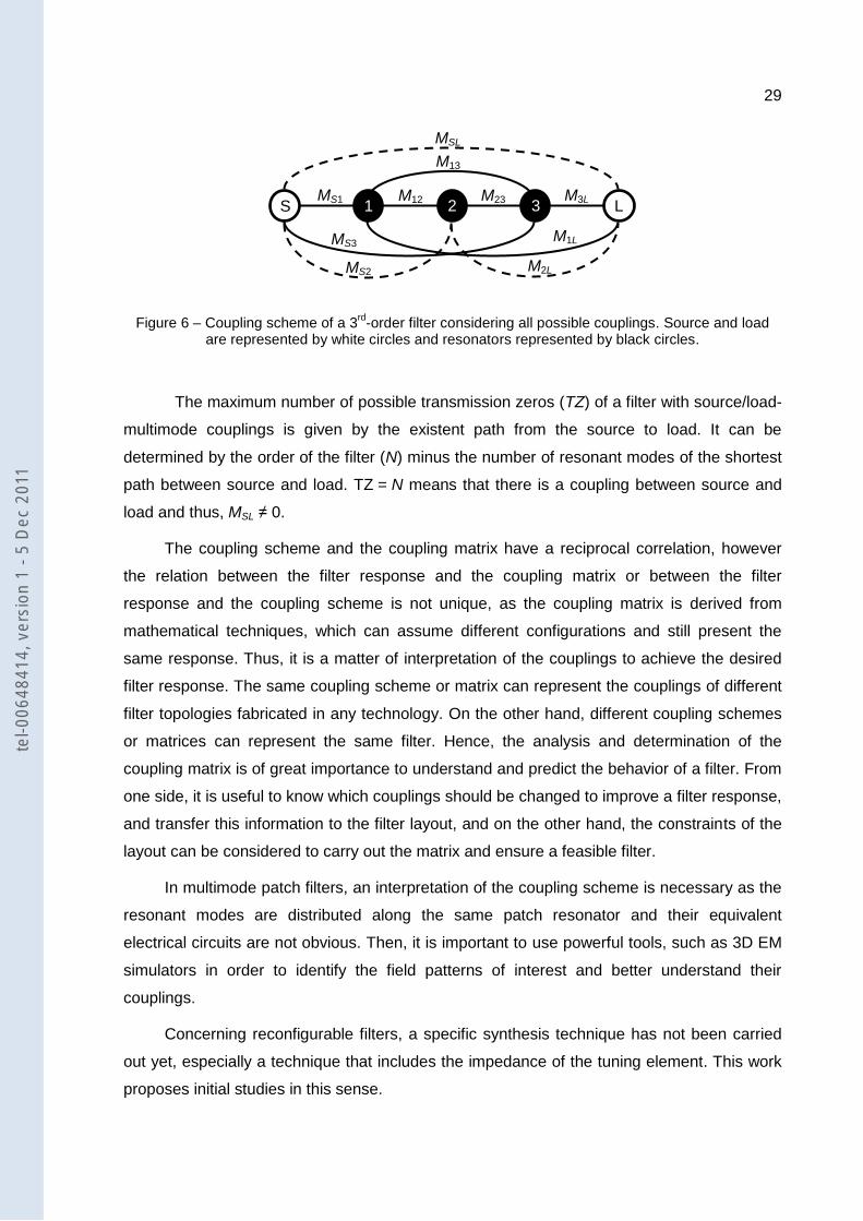
29
Figure 6 – Coupling scheme of a 3rd
-order filter considering all possible couplings. Source and load are represented by white circles and resonators represented by black circles.
The maximum number of possible transmission zeros (TZ) of a filter with source/load-
multimode couplings is given by the existent path from the source to load. It can be
determined by the order of the filter (N) minus the number of resonant modes of the shortest
path between source and load. TZ = N means that there is a coupling between source and
load and thus, MSL ≠ 0.
The coupling scheme and the coupling matrix have a reciprocal correlation, however
the relation between the filter response and the coupling matrix or between the filter
response and the coupling scheme is not unique, as the coupling matrix is derived from
mathematical techniques, which can assume different configurations and still present the
same response. Thus, it is a matter of interpretation of the couplings to achieve the desired
filter response. The same coupling scheme or matrix can represent the couplings of different
filter topologies fabricated in any technology. On the other hand, different coupling schemes
or matrices can represent the same filter. Hence, the analysis and determination of the
coupling matrix is of great importance to understand and predict the behavior of a filter. From
one side, it is useful to know which couplings should be changed to improve a filter response,
and transfer this information to the filter layout, and on the other hand, the constraints of the
layout can be considered to carry out the matrix and ensure a feasible filter.
In multimode patch filters, an interpretation of the coupling scheme is necessary as the
resonant modes are distributed along the same patch resonator and their equivalent
electrical circuits are not obvious. Then, it is important to use powerful tools, such as 3D EM
simulators in order to identify the field patterns of interest and better understand their
couplings.
Concerning reconfigurable filters, a specific synthesis technique has not been carried
out yet, especially a technique that includes the impedance of the tuning element. This work
proposes initial studies in this sense.
1
3 2 S L
MSL
MS1 M12 M23 M3L
MS3 M1L
M2L MS2
M13
tel-0
0648
414,
ver
sion
1 -
5 D
ec 2
011
30
3.2 METHODOLOGY
The design of tunable patch filters is not simple because their equivalent circuits are
not obvious to extract due to the geometry of the resonator. The formulation of patch
resonators is applied to unperturbed geometries and the usual practice of modifying the
patch resonator geometry with cuts and slots turns out to be excessively complex. Thus, the
approach used for the design of tunable microstrip filters cannot be used to design a patch
filter, much less to design tunable patch filters. It is difficult to analyze all the couplings in a
patch filter independently, due to the simultaneous presence of the modes in the same
resonator. There is not an effective method that isolates the equivalent electrical circuit of
each mode and relates it to a specific part of the filter layout. Even harder is to assess the
effect of a tuning element on one or more modes of the patch resonator. In view of this, a
methodology is proposed and presented here to help on the analysis and design of tunable
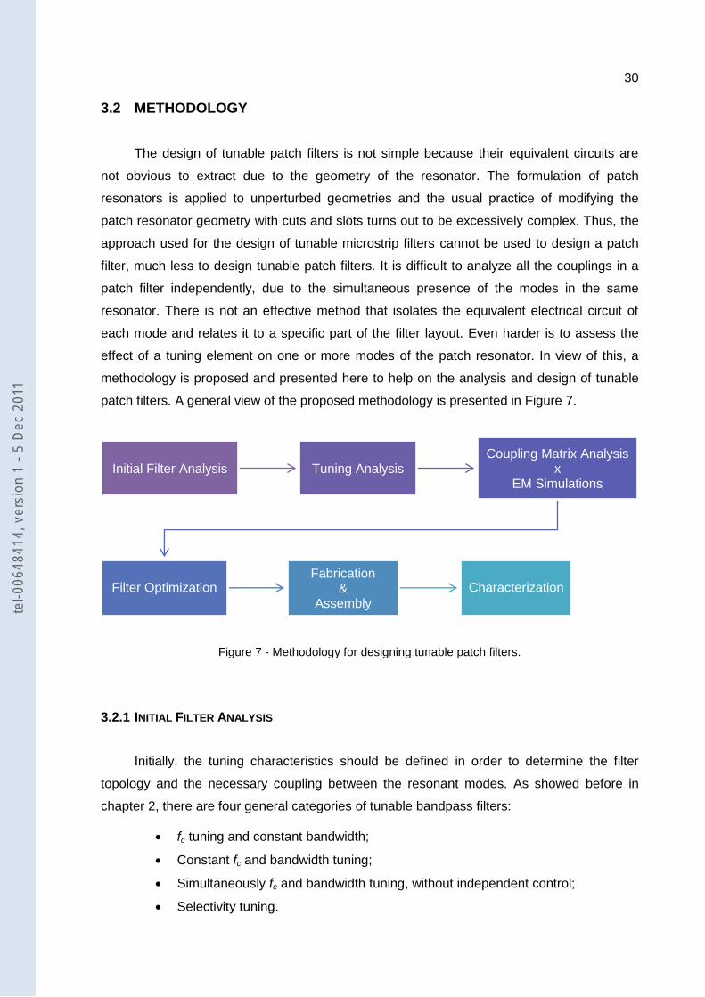
patch filters. A general view of the proposed methodology is presented in Figure 7.
Figure 7 - Methodology for designing tunable patch filters.
3.2.1 INITIAL FILTER ANALYSIS
Initially, the tuning characteristics should be defined in order to determine the filter
topology and the necessary coupling between the resonant modes. As showed before in
chapter 2, there are four general categories of tunable bandpass filters:
fc tuning and constant bandwidth;
Constant fc and bandwidth tuning;
Simultaneously fc and bandwidth tuning, without independent control;
Selectivity tuning.
Initial Filter Analysis Tuning Analysis Coupling Matrix Analysis
x EM Simulations
Filter Optimization Fabrication
& Assembly
Characterization
tel-0
0648
414,
ver
sion
1 -
5 D
ec 2
011

31
For each type of tuning goal, there is a different design technique. The technique for
designing filters with center frequency tunability involves the change of the electrical length of
the resonators. The technique for tuning the filter bandwidth is more complex because it
involves the change of inter-resonator couplings, which cannot always be done individually,
affecting the overall response of the filter. In practice, sometimes, the design does not allow
the change of the filter center frequency without changing its bandwidth, and vice-versa. If
this behavior is not acceptable, another topology should be selected.
The initial resonator and its physical dimensions are determined according to the
desired operating frequency for the filter. The dimensions can be calculated from the
equations given in section 2.2, with initial perturbations chosen by considering the electric
field patterns along the resonator. The design process involves iterative steps in order to
achieve the desired characteristics. The coupling between the resonant modes is determined
by inserting perturbations to the patch geometry, such as slots, cuts, or adding small
patches. This should be carefully analyzed in order to understand how the perturbations
change the modes coupling.
3D-EM simulators provide a full electromagnetic response of any kind of structure and
all the couplings involved in the layout. Among the commercial available 3D-EM simulators,
the Advanced Design System (ADS) software, from Agilent Technologies, was chosen to be
used in this work. In ADS, there are two types of 3D-EM simulators. A 3D full-wave EM
simulator based on the Finite Element Method, called FEM, and a 3D-planar frequency-
domain simulator based on the Method of Moments, called Momentum. Only Momentum was
used due to the excellent trade-off between results accuracy and simulation time for the type
of structures simulated in this work. Besides the accurate filter frequency response, it also
allows different analysis required for the design of tunable patch filters by setting the right
layout and parameters, as it will be further explained in this chapter.
The traditional EM analysis consists in simulating the filter layout and changing its
geometry in a way to obtain the desired couplings. For the design of tunable patch filters, the
focus is to find one or more perturbations, which variations on its dimensions will result in the
behavior for the desired tunable patch filter. The tuning element will be later integrated to the
perturbations in order to electronically change them and control the selected characteristics.
These initial simulations are lossless, which means that they do not consider any substrate
loss. The losses will be considered at the last step of the methodology, so the loss origin in
the filter response can be correctly assessed.
An interpretation of the EM simulations is necessary to determine the nature of the
coupling existing between the resonant modes and the feed lines in the patch resonator and
tel-0
0648
414,
ver
sion
1 -
5 D
ec 2
011

32
then define the corresponding coupling topology for the filter. The interpretation also allows
the extraction of some parameters, such as the resonant frequency f of each mode when
coupled to other modes, the external quality factors evaluated at the individual resonant
frequencies, the self-resonant frequency f0 of each mode, etc. This is of great importance
because the parameters extracted from the simulations are used to calculate the initial
coupling matrix coefficients.
Simulations of the filter using the feed lines weakly coupled to the resonator give the
resonant frequencies f of each mode when coupled to other modes. On the other hand, the
self-resonant frequencies f0 of each mode can be excited by using the method of placing a
magnetic wall or an electric wall in the filter symmetry axis52. This will excite only the even
modes or the odd modes, respectively. Unfortunately, ADS does not have a tool to simulate
symmetric electric and magnetic boundaries. Then, HFSSTM, from Ansoft, another 3D full-
wave EM simulator was used for this specific simulation. The simulations carried out with
HFSS were used as a confirmation of the theory and particularly in this work, were not
essentially necessary.
A more careful inspection of eq. (25) leads to some interesting inferences regarding the
coupling between two resonant modes A and B. If the filter is synchronously tuned, where all
resonant modes have the same frequency (f0A = f0B), then the equation is reduced to the well-
known formula given in eq. (28).
(28)
On the other hand, if the filter is asynchronously tuned, where each resonant mode has
a different frequency (f0A ≠ f0B), the equation is more complex, and is calculated as given in
eq. (25). This is the case of the filters studied in this work. Moreover, if the modes are
uncoupled, their coupling coefficient is null (MAB = 0), and thus, f0A = fA and f0B = fB. This is an
important observation, which leads to the choice of the coupling scheme of the filter.
Finally, by exciting the structure with only one of the feed lines, it is possible to
determine the external quality factor Qe by extracting the coupling between the feed line and
the excited modes. A well-known method for calculating Qe from the S11 curve of the filter is
by measuring the bandwidth Δf±90⁰ where the mode phase changes ± 90⁰ with respect to the
phase of the resonant frequency fA 53:
tel-0
0648
414,
ver
sion
1 -
5 D
ec 2
011

33
(29)
With the equations given in this section, in addition to those given in section 3.1, an
initial coupling matrix can be built and its coefficients adjusted so that its frequency response
matches the simulated curve from the 3D EM simulator. All the curves presented in this work
were simulated in Momentum – ADS, except where indicated.
Because the coupling matrix coefficients are frequency-independent, the center
frequency and bandwidth of the filter are considered only when calculating the de-normalized
theoretical frequency response of the filter using equations (20) to (23). A Matlab routine for
a general filter of order N was developed for this purpose. It can be found in the appendix of
the thesis.
3.2.2 TUNING ANALYSIS
The tuning analysis consists in determining the tuning element, which can be varactor
diodes, MEMS switches or capacitances, PIN diodes, or any type of commercial or custom
device that changes the filter response as the desired tuning behavior.
There are mainly two ways to simulate the tuning elements: by either drawing the
structure integrated to the filter layout or using its equivalent electrical model. The simulation
results indicate the appropriated position of the tuning element in the filter layout, its range of
values for the desired filter operation, the dimensions of the tuning element, the influence of
packaging or wire bonding, depending on the tuning element used.
When using the equivalent electrical circuit model, first, the tuning element should be
characterized in order to extract its equivalent electrical model. Then, another simulation
procedure must be used because the EM simulator Momentum does not allow the
connection of lumped elements, such as resistors, inductors, or capacitors, directly in the
layout. In order to verify the influence of the tuning element in the filter response, electrical
simulations are performed in the ADS schematic environment considering the previous EM
simulations performed at Momentum. For that, in Momentum, internal ports are placed in the
filter layout where the lumped elements should be connected, as shown in Figure 8.
tel-0
0648
414,
ver
sion
1 -
5 D
ec 2
011

34
Figure 8 – Filter layout in Momentum environment with two single-mode ports (input and output) and several internal ports where the lumped elements of the tuning element model can be connected in
the schematic environment.
After the regular EM simulation, a model of this layout is generated encompassing the
S-parameters matrix over the entire frequency range simulated in Momentum. The model
becomes available to be imported into the schematic environment. Then, lumped tuning
elements can be connected to the model’s ports, and the electrical simulations can be
performed considering the previous EM results, as shown in Figure 9.
Figure 9 – Filter model with the S-parameters matrix imported to the schematic environment, ADS, with lumped tuning elements connected to the internal ports.
Single-mode ports
Internal ports
P8
P9
tel-0
0648
414,
ver
sion
1 -
5 D
ec 2
011

35
3.2.3 COUPLING MATRIX ANALYSIS VERSUS EM SIMULATIONS
Through the coupling matrix, it is possible to change the coupling coefficients in order
to verify their effect on the filter response and compare to the effect of each tuning element
on the simulation. This theoretical analysis allows us to verify what kind of frequency
responses the filter under analysis is able to produce.
The principle followed in the design is to force the element under consideration in the
layout to give the same response as the corresponding coefficients in the coupling matrix, or
vice-versa, at least over a small range of frequencies around the passband. The proposed
design methodology is based on the determination of a specific coupling by matching the
scattering parameters of the corresponding elements in the coupling matrix with those
obtained from the complete simulations of the structure until the desired frequency response
is achieved.
The simulations at this point are the most complete ones, including the equivalent
electrical model of the tuning elements, extracted in a step before, and the substrate losses.
A trial version of commercial software, called CoupleFil54, was used to synthesize the
coupling matrix and verify the method presented here. Basically, the software asks for the
filter order and frequency response characteristics to generate a coupling matrix
corresponding to a given coupling scheme. It also provides a tool to calculate the scattering
parameters curves from a coupling matrix with the choice of using resonators with infinite or
finite Q.
3.2.4 FILTER OPTIMIZATION
The filter optimization procedure corresponds to a recursive process carried out in each
step of the design methodology. During the simulations and coupling matrix analysis, the
filter design should be changed in order to meet the desired parameters for the final tunable
filter. The modifications should concern the type of perturbation if the nature of the coupling
is not the expected one, or concern only dimensions of the perturbations or of the resonator if
the tuning range is out of range. The tunability of the tuning element should be also
considered in the optimization process in order to match the tuning requirements.
Lastly, the layout is modified to allow the connection of the tuning elements and the
application of the bias voltage. Sometimes these modifications can affect the filter response,
thus the filter should be simulated considering them. Only after, the filter is ready to be
fabricated.
tel-0
0648
414,
ver
sion
1 -
5 D
ec 2
011

36
3.2.5 FABRICATION AND ASSEMBLY
The patch filters designed were manufactured using two different processes: chemical
or mechanical.
In the chemical process, a flexible mask is generated from the designed layout and
recorded on the substrate using traditional photolithographic process. The copper layer of the
substrate is selectively protected with a photoresist and then etched in a chemical solution of
ferric chloride. This process has low precision, highly operator dependent, and therefore not
reproducible. However, it can be used with satisfactory results in topologies with dimensions
larger than 300 µm, and with layouts where small variations in the dimensions are not critical
for the device performance.
The mechanical process uses a computer controlled micro-milling machine that cuts
out the required regions of the substrate to form the filter topology informed by dedicated
software. This process is highly accurate, with a precision of the order of 1 µm, highly reliable
and reproducible. Gaps smaller than 100 µm are feasible with this machine.
In order to facilitate the filters fabrication, reduce costs and make them commercially
attractive, commercial microwave flexible substrates were also used, providing flexibility to
the filters design.
After the fabrication process, the tuning elements and the bias circuit components were
directly soldered on the device.
3.2.6 CHARACTERIZATION
The fabricated filters were characterized by measuring their scattering parameters as a
function of frequency. The measurements were performed using Vector Network Analyzers
from Agilent Technologies, HP8722D and HP8510C, available at the laboratories at the
Polytechnic School of USP and at IMEP-LAHC.
Another important characterization performed in this work was the filter performance
with increasing power levels. The filter performance is affected by the nonlinear behavior of
tuning elements added to the patch resonators, as varactor diodes. In order to investigate the
power capability of the designed tunable patch filters, the 1-dB compression point (P1dB) and
the 3rd order intermodulation component levels were experimentally determined.
The tunable patch filter’s P1dB was measured with the setup presented in Figure 10.
tel-0
0648
414,
ver
sion
1 -
5 D
ec 2
011

37
Figure 10 – Setup for the measurement of the 1-dB compression point.
The signal distortion of the tunable patch filters was investigated using the
measurement setup shown in Figure 11.
Figure 11 – Setup configuration for the measurement of the third-order intercept point.
3.2.7 CHAPTER SUMMARY
In this chapter, the proposed methodology for designing tunable patch filters was
detailed. The methodology consists on the analysis of the resonant modes that form the filter
passband. It provides the techniques to extract the coupling scheme that models the filter
behavior and the necessary equations for calculating the corresponding coupling matrix. For
that, EM simulations are of major importance. In this methodology, the lossless simulations
should be compared to simulations considering the substrate dielectric and conductor losses
and the equivalent electrical model of the tuning element in order to assess their effects.
Then, a theoretical study analyzing the coupling matrix coefficients should be used for
comparison with the simulation results considering the tuning elements. This allows the
correct model of the tuning effect and the definition of the tuning possibilities and limits.
The fabrication and assembly of the filters proposed in this work do not demand any
particular process, using traditional photolithography on commercial microwave substrate.
The characterization is made at small signals, measuring the S-parameters versus
frequency. Nonlinear measurements at higher power levels are also performed in order to
determine the 1-dB compression point and the third-order intercept point.
This methodology is applied to the design, fabrication and characterization of a tunable
dual-mode triangular patch filter, detailed in chapter 4, and a tunable triple-mode circular
patch filter detailed in chapter 5.
Synthesizer DUT Power Meter -10 dB 25 dB
Synthesizer 1
Synthesizer 2 -6 dB
-6 dB Combiner
DUT Spectrum Analyzer
tel-0
0648
414,
ver
sion
1 -
5 D
ec 2
011

38
4 TUNABLE TRIANGULAR PATCH FILTER WITH INDEPENDENT
CENTER FREQUENCY AND BANDWIDTH CONTROLS
This section describes the design of a tunable dual-mode bandpass miniaturized patch
filter, with independent tunability of center frequency and bandwidth, both with continuous
control. The tunable patch filter, initially centered at 3.8 GHz, uses a modified equilateral
triangular resonator with capacitances placed along the slots etched in the patch. All the
simulations were made using the Rogers Duroid substrate RO3210 with a thickness of
25 mils, and a dielectric constant εr = 10.2.
The chosen topology was proposed in my master dissertation using a triangular patch
resonator with an inverted “T” shape slot34. Some other designs of triangular patch filters with
slots were also presented in the literature55, 56. However, the use of the inverted T shape slot
provides two transmission zeros around the passband, improving the filter rejection, and
allows a greater miniaturization compared to both previous works.
4.1 INITIAL FILTER ANALYSIS
The degenerate fundamental modes in a triangular patch resonator without
perturbations, presented in Figure 12, clearly distinguishing the odd (a) and the even (b)
modes. The corresponding current distributions simulated with a weak coupling between the
input/output and the resonator are also shown in this figure.
Figure 12 – Unperturbed electrical field pattern (left) and the corresponding current distribution (right) (a) Odd-mode and (b) Even-mode.
max
0
min
(a)
(b)
max
0
min
tel-0
0648
414,
ver
sion
1 -
5 D
ec 2
011
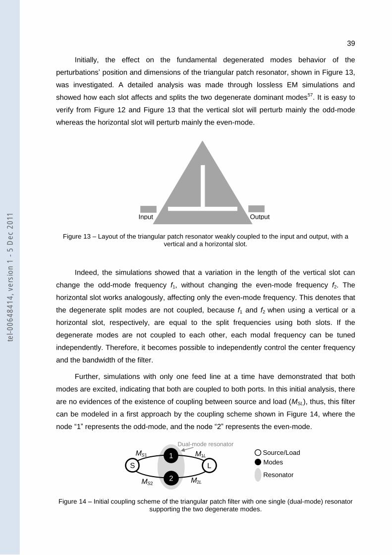
39
Initially, the effect on the fundamental degenerated modes behavior of the
perturbations’ position and dimensions of the triangular patch resonator, shown in Figure 13,
was investigated. A detailed analysis was made through lossless EM simulations and
showed how each slot affects and splits the two degenerate dominant modes57. It is easy to
verify from Figure 12 and Figure 13 that the vertical slot will perturb mainly the odd-mode
whereas the horizontal slot will perturb mainly the even-mode.
Figure 13 – Layout of the triangular patch resonator weakly coupled to the input and output, with a vertical and a horizontal slot.
Indeed, the simulations showed that a variation in the length of the vertical slot can
change the odd-mode frequency f1, without changing the even-mode frequency f2. The
horizontal slot works analogously, affecting only the even-mode frequency. This denotes that
the degenerate split modes are not coupled, because f1 and f2 when using a vertical or a
horizontal slot, respectively, are equal to the split frequencies using both slots. If the
degenerate modes are not coupled to each other, each modal frequency can be tuned
independently. Therefore, it becomes possible to independently control the center frequency
and the bandwidth of the filter.
Further, simulations with only one feed line at a time have demonstrated that both
modes are excited, indicating that both are coupled to both ports. In this initial analysis, there
are no evidences of the existence of coupling between source and load (MSL), thus, this filter
can be modeled in a first approach by the coupling scheme shown in Figure 14, where the
node “1” represents the odd-mode, and the node “2” represents the even-mode.
Figure 14 – Initial coupling scheme of the triangular patch filter with one single (dual-mode) resonator supporting the two degenerate modes.
Input Output
Dual-mode resonator
MS1 M1L
MS2 M2L
S L
1
2
Source/Load
Modes
Resonator
tel-0
0648
414,
ver
sion
1 -
5 D
ec 2
011

40
The maximum center frequency of the filter was specified to be 3.8 GHz. The filter was
initially optimized to reach this frequency by adjusting the slots dimensions and the position
of the feed lines, as illustrated in Figure 15. The substrate considered was the RogersTM
substrate RO3210 with thickness of 25 mils, and dielectric constant εr = 10.2, initially without
losses. The filter frequency response is shown in Figure 16. The filter is centered at 3.8 GHz,
with a very narrow bandwidth of 1.4 %. Two transmission zeros (TZs) at real frequencies are
located at each side of the passband at 3.2 GHz and 4.0 GHz, respectively. The current
distribution of each mode showed that the even-mode exhibits a lower frequency than the
odd-mode.
Figure 15 – Layout of the triangular patch filter with dimensions in mm.
Figure 16 – Frequency response of the triangular patch filter from the EM simulations without considering any substrate loss.
The two TZs in the frequency response of this second order filter (TZ = N = 2) show
that the source is coupled to the load (MSL ≠ 0). This is a parasitic coupling that is due to the
presence of higher modes in the structure, which provide additional paths between the input
and output. The parasitic coupling is much weaker than the other coupling coefficients in the
Input Output
12
1.5 0.5
0.5 5.18
9.16
0.55
-70
-60
-50
-40
-30
-20
-10
0
2.5 3 3.5 4 4.5Frequency (GHz)
Mag
nit
ud
e (
dB
) S21 Simulated
S11
Simulated odd-mode
even-mode
tel-0
0648
414,
ver
sion
1 -
5 D
ec 2
011

41
structure, as the positions of the two TZ demonstrate. The stronger this coupling, the closer
the TZ are to the center frequency.
Finally, the complete scheme of the triangular patch filter is presented in Figure 17.
Figure 17 – Complete coupling scheme of the triangular patch filter with one single (dual-mode) resonator supporting the two fundamental degenerate modes.
The coupling matrix format corresponding to this coupling scheme is given in (30).
From the initial analysis of the degenerate mode patterns, it should be expected that for the
odd-mode MS1 = -M1L and for the even-mode MS2 = M2L. Using specialized software54, the
coupling values were calculated considering a RL of 10 dB to match the simulated frequency
response. The resulting coupling matrix is given in (31), denoted by MΔ, where the index Δ
was used to refer to the triangular resonator. These values are consistent with the equations
and techniques presented in chapter 3, confirming the interest of using EM simulations to
calculate the matrix coefficients.
The theoretical frequency response of the filter calculated from (22) and (23) are
presented in Figure 18 considering the filter centered at 3.8 GHz and with FBW3dB of 1.4 %,
and the frequency response obtained from EM simulations neglecting any dielectric and
conductor losses of the substrate. Both curves are in very good agreement, hence
corroborating this analysis.
[
] (30)
[
] (31)
It can be seen in the inset in Figure 18 that there is a difference of approximately 1 dB
in the passband IL between the lossless simulated curve and the theoretical curve. As
neither conductor nor dielectric losses were considered in the EM simulations, and because
Dual-mode resonator
MS1 M1L
MS2 M2
MSL S L
1
2
Odd-mode
Even-mode
tel-0
0648
414,
ver
sion
1 -
5 D
ec 2
011

42
the feed lines are capacitively coupled to the resonator, this difference represents the
radiation loss. This can be compensated by increasing the coupling between feed lines and
resonator, as discussed further in section 4.4.
Figure 18 – Simulated (lossless substrate) and theoretical (from matrix MΔ in (31)) responses of the triangular patch filter. An inset of the passband is shown on the upper right corner.
From the calculated coupling matrix in (31), it is possible to verify the very weak
coupling between source and load through the very low MSL value of -0.0036. Besides, the
asymmetrical frequency response is verified by MS1 ≠ MS2. The elements M11 < 0 and M22 > 0
implies that fodd > feven, confirming the EM simulation results presented in Figure 16, where the
odd-mode frequency is higher than the even-mode frequency.
Moreover, the filter exhibited two transmission zeros at real frequencies located at each
side of the passband. If the mode frequencies are changed in a manner that fodd < feven, the
transmission zeros are moved to imaginary frequencies, as seen in the frequency response
in Figure 19(a), as a result of the coupling matrix (31) where only the signs of M11 and M22
were changed. When fodd = feven, M11 = M22 = 0, there is a destructive superposition of both
modes at the central frequency, leading to a significant rejection at the center frequency, as
seen in Figure 19(b).
Figure 19 – Theoretical responses of the triangular patch filter when (a) fodd < feven and (b) fodd = feven.
-70
-60
-50
-40
-30
-20
-10
0
2.5 3 3.5 4 4.5
Magnitude (
dB
)
Frequency (GHz)
S21 Theory S11 Theory S21 Simulated S11 Simulated
fodd > feven
-70
-60
-50
-40
-30
-20
-10
0
2.5 3.5 4.5-100-90-80-70-60-50-40-30-20-10
0
2.5 3.5 4.5Frequency (GHz)
Mag
nit
ud
e (
dB
)
Frequency (GHz)
Mag
nit
ud
e
(dB
)
(a) (b)
S11
Theory
S21
Theory
S11
Theory
S21
Theory
fodd
< feven
fodd
= feven
-5
-4
-3
-2
-1
0
3.6 3.7 3.8 3.9 4
tel-0
0648
414,
ver
sion
1 -
5 D
ec 2
011

43
4.2 TUNING ANALYSIS
In order to realize a tunable filter, the capacitances C1, and C2 were positioned across
the slots of the triangular resonator. Their influence on the filter response was investigated.
As shown in Figure 20, only one capacitance was placed across the vertical slot, and two
capacitances were placed across the horizontal slot to keep the filter symmetry in respect to
the S-S’ plane.
Figure 20 – Triangular patch filter with tuning capacitances at the (a) edge of each slot, (b) middle of the slots, and (c) junction of the slots.
The simulation results showed that C1 controls the odd-mode’s frequency without
changing the even-mode’s frequency. On the contrary, C2 controls the even-mode’s
frequency without changing the odd-mode’s frequency. This very important behavior means
that it is possible to control the filter center frequency and bandwidth independently by
choosing the correct set of capacitances. This high degree of freedom is only possible since
the fundamental modes are uncoupled.
The change in modal frequencies is affected by the capacitances, as well as their
position across the slots. Table 4.1 shows the influence of the capacitances’ position on the
tuning range, considering the filter frequency response with RL better than 10 dB. In the
simulations, the IL slightly barely changed. For higher capacitances than the ones shown in
Table 4.1, the RL becomes worse than 10 dB due to the mismatch of the resonator
impedance. The simulated results in this table show that a maximum center frequency tuning
range of 29 % is obtained when the capacitances are positioned in the middle of the slots.
In order to compare the influence of the capacitances in the center frequency
response, the capacitances were also assessed within the same tuning range of 4 % from
3.81 GHz to 3.66 GHz at the three positions considered in Figure 20. Table 4.1 shows that for
this range, a broader capacitance variation is needed when the capacitances are placed at
the edge of the slots than when they are positioned closer to the slots junction. This is quite
obvious, but very important. When the capacitors are placed at the edge of the slots, they are
In Out
C1
C2 C
2
S
S’
In Out
C
1
C2 C
2
S
S’
In Out
C
1
C2 C
2
S
S’
(a) (b) (c)
tel-0
0648
414,
ver
sion
1 -
5 D
ec 2
011

44
short-circuited by the end of the slots, and hence their influence on the resonant modes is
weak. Inversely, the maximum sensitivity is obtained for capacitances placed at the slots
junction. This important observation explains the effect of the series resistance when using a
real model of the tuning element, for example a capacitor. The filter loss due to a capacitor’s
series resistance increases when the capacitor is moved towards the slots’ junction, where
their influence is stronger.
Table 4.1 – Simulated center frequency and capacitance ranges for different positions of the capacitances C1, and C2 along the slots of the triangular patch filter.
Capacitance position Capacitance range
(pF) Center frequency range
(GHz) Tuning range
(%)
Edges of slots 0 – 0.92 3.81 – 3.66 4 (max. range)
Middle of slots 0 – 1.45 3.81 – 2.85 29 (max. range)
0 – 0.27 3.81 – 3.66 4
Junction of slots 0 – 0.20 3.81 – 3.52 8 (max. range)
0 – 0.08 3.81 – 3.66 4
In practice, it could be interesting to use several capacitances for a coarse- or fine-
tuning, although for simplicity, the filter was designed with capacitances in the middle of the
slots, providing a large tuning range with a well-matched response.
4.3 VARACTOR DIODE MODEL
The tuning element used in this filter was a varactor diode. Varactor diode is a
semiconductor diode that, when reversed biased below its breakdown voltage, acts as a
voltage-controlled variable capacitance. The reverse voltage changes the width of its
depletion layer, changing the diode junction capacitance.
There is a characteristic curve of the junction capacitance Cj versus the reverse bias
voltage V specific to each type of diode, following eq. (32).
( ⁄ ) (32)
Where:
Cj is the reverse biased variable junction capacitance;
Cj0 is the junction capacitance without an external bias;
V is the applied reverse bias voltage;
tel-0
0648
414,
ver
sion
1 -
5 D
ec 2
011

45
Vj is the built-in junction potential;
γ “gamma” is a coefficient relating Cj and V. It depends on the junction doping profile.
When modeling an encapsulated varactor diode, one should take into account the
parasitic elements that are mostly due to the package, in order to obtain an accurate
equivalent electrical circuit model at the frequency band at which the diode will operate. For
the filters developed in this work, the classical model used is shown in Figure 21, where Rs
represents the parasitic series resistance of the diode die, Ls and Cp are the parasitic
inductance and capacitance due to the package. In this model, Rs and Ls vary with the
applied voltage. In general, the capacitance Cp is absorbed by Cj due to its very low value,
and the model becomes a simple series RLC. At higher microwave frequencies, say above
10 GHz, a more complete model should be extracted, taking into account Cp, the package
material, the wires bonding, etc.
Figure 21 – Equivalent electrical model of a reversed biased varactor diode.
Normally, a typical curve Cj (V) is given by the manufacturer for each varactor diode, as
shown in Figure 22. With these curves, the more suitable diode capacitance values can be
chosen for the design of the reconfigurable filters.
Figure 22 - Example of curves Cj (V) for varactor diodes modelled at 1 MHz given by the manufacturer (MA46H071, from M/A-COM, used in this work).
Cj Rs Ls
Cp
tel-0
0648
414,
ver
sion
1 -
5 D
ec 2
011

46
Figure 22 shows the curve of the MA46H071 GaAs diode, from M/A-COM, which was
available to be used in this work. The available data given by the manufacturer is the
capacitance range vs. the reverse voltage from 0.45 pF (20 V) to 2.3 pF (0.1 V) at 1 MHz,
γ = 0.75, Ls = 0.45 nH, and Q = 4500 (at 50 MHz). The Q-factor is defined in eq. (33).
(33)
The capacitance range of this varactor diode is slightly above the values defined by the
simulations. In order to use it, a configuration with two series varactor diodes is used as
illustrated in Figure 23, halving the total capacitance. The varactor diodes were connected to
ground by a 10 kΩ resistor in order to provide the DC path while blocking the RF signal to
ground. A back-to-back configuration was necessary as both sides of the slots are at the
same potential, which would prevent biasing the diodes if directly placed across the slots.
Furthermore, the back-to-back configuration has been proven to improve the linearity
performance, increasing the power handling of the device and improving the 1-dB
compression point and the third-order interception point (IIP3)58, 29.
Figure 23 – Back-to-back configuration of the varactor diodes to allow biasing and improve linearity.
This diode was characterized to extract its RsLsCj model by measuring its S-parameters
for different reverse bias voltages. Then, the RsLsCj model was simulated in ADS and the
values of Rs, Ls and Cj were adjusted so that the simulated S-parameters fit the measured
data. The capacitances found at 2.45 GHz, presented in Figure 24, are slightly different from
those of the manufacturer. The measurements showed that Rs varies from 1.7 Ω (at 1 V) to
3 Ω (at 20 V), Ls varies from 1.2 nH (at 1 V) to 1.7 nH (at 20 V), and hence, Q varies from 24
(at 1 V) to 54 (at 20 V). Despite the changes in Rs and Ls, the values used to simulate the
real varactor diode were constant, with Rs = 2 Ω, and Ls = 1.3 nH. This resulted in very good
predicted responses and it was not necessary to complicate the model.
R
V
tel-0
0648
414,
ver
sion
1 -
5 D
ec 2
011

47
Figure 24 – Measured Capacitance x Reverse Voltage for the varactor diode MA46H71 at 2.45 GHz.
Some simulations were made in order to verify the effect of the parasitic resistance and
inductance of the varactor diode’s equivalent electrical model. As expected, when the series
resistance was varied from 0 Ω to 3 Ω, it increased the filter’s insertion loss. The variation in
insertion loss changed with the increase of the capacitance and with its position across the
slots, as previously explained. For the same capacitance, if Rs is varied from 0 Ω to 3 Ω, the
insertion loss varies 0.17 dB when the varactor diodes are located at the edge of the slots,
0.6 dB when the varactor diodes are located in the middle of the slots, and 2 dB when the
varactor diodes are located at the slots junction.
4.4 THEORETICAL ANALYSIS & EM SIMULATIONS
The filter was simulated considering the real losses of the RogersTM RO3210 substrate.
The dielectric loss provided by the manufacturer is tan δ = 0.0027 and the conductor loss is
given by the thickness of the metal layer, 17 µm, and the copper conductivity, 5.8x10⁻⁷ S/m.
The filter is very sensitive to the conductor and dielectric losses, as shown in Figure 25.
Figure 25 – Effect of the dielectric and conductor losses in the passband of the triangular patch filter.
0.3
0.5
0.7
0.9
1.1
1.3
1.5
1.7
0 2.5 5 7.5 10 12.5 15 17.5 20C
apacitance (
pF
)
Reverse Voltage (V)
MA46H71
-20
-18
-16
-14
-12
-10
-8
-6
-4
-2
0
3.6 3.7 3.8 3.9 4.0
Magnitude (
dB
)
Frequency (GHz)
No Substrate Losses
Dielectric Loss (tan = 0.0023)
Conductor Loss
Dielectric+Conductor Losses
Dielectric Loss (tan = 0.016)
tel-0
0648
414,
ver
sion
1 -
5 D
ec 2
011

48
Figure 25 shows that due to the substrate losses, the IL increased to 5 dB. In order to
minimize this loss, two capacitors Cin were placed between the feed lines and the resonator
strengthening this coupling and the coupling between the source and the load. This allows a
stronger coupling without positioning the feed lines extremely close to the resonator, thus
facilitating the fabrication process. On the other hand, Cin enlarges the filter bandwidth and
also decreases the out-of-band rejection. The tunable dual-mode filter was then optimized
with the configuration illustrated in Figure 26.
Figure 26 - Tunable dual-mode filter using a single triangular patch resonator with varactors across the slots. In detail, the assembling scheme of the varactors.
Different tuning ranges can be achieved when different values of Cin are considered.
This capacitor was also modeled and characterized as a series RLC circuit, where R = 0.2 Ω,
L = 0.3 nH. Cin was chosen to be 1.8 pF. Figure 27 shows the simulated filter response
considering the RLC model of Cin. The center frequency was reduced to 3.7 GHz and the
FBW3dB enlarged to 10 %.
Figure 27 – Simulated filter response considering the substrate losses and the RLC series model of Cin, where R = 0.2 Ω, L = 0.3 nH, and Cin = 1.8 pF.
-40
-30
-20
-10
0
2.5 3 3.5 4 4.5
Magnitude (
dB
)
Frequency (GHz)
S21 Simulated S11 Simulated
Port 1 Port 2
Cin Cin
C1
C2 C
2
R
V1
tel-0
0648
414,
ver
sion
1 -
5 D
ec 2
011

49
Figure 28 shows two theoretical curves considering Cin. One curve considers an infinite
Q resonator, and the other, a finite Q = 90 resonator, resulted from matrix (34). Note that the
theoretical curves considering a real resonator with finite Q are very close to the simulated
one. Hence, it can be estimated that the varactor loaded resonator’s Q is near 80. This value
is quite good compared to that of microstrip tunable resonators.
[
] (34)
Figure 28 – Theoretical curves from (34), considering a resonator with infinite Q and finite Q = 80.
As expected, due to Cin, the magnitude of MSL in the new matrix (34) highly increased
when compared to the initial matrix (31). M22 increased as well, making the feven-mode
decrease, explaining the decrease in the center frequency. M11 barely changed, explaining
the increase in the filter bandwidth. The values of MS1 and MS2 increased as well.
A coupling matrix analysis was made in in order to verify the effect of the coupling
coefficients in the filter frequency response. This analysis leads to three important
observations:
M11 only changes the odd-mode, and M22 only changes the even-mode, as
expected according to (24), allowing their independent control. This is feasible
because C1 controls the odd-mode, represented by M11, and C2 controls the
even-mode, represented by M22. This control will be shown later in this section.
The FBW3dB is a linear function of (M22 - M11). This observation implies that by
increasing M11 and M22 by the same amount u, filters with the same FBW3dB and
-50
-40
-30
-20
-10
0
2.5 3 3.5 4 4.5
Magnitude (
dB
)
Frequency (GHz)
S21 Simulated S11 Simulated S21 Theory S11 Theory S21 Theory, finite Q S11 Theory, finite Q
tel-0
0648
414,
ver
sion
1 -
5 D
ec 2
011

50
decreasing center frequencies can be designed (and vice-versa). This can be
seen in the theoretical curves obtained from matrix (35), in Figure 29.
[
] (35)
Figure 29 – Theoretical curves for filters with the same FBW3dB and different center frequencies for u = 4, u = 0 and u = -3 from matrix (35).
The center frequency is a linear function of (M22 + M11)/2. This observation
implies that filters with same center frequency and increasing bandwidths are
achievable by decreasing M11 and increasing M22 by the same amount z (and
vice-versa). This can be seen in the theoretical curves obtained from matrix
(36), shown in Figure 30.
[
] (36)
Figure 30 – Theoretical curves for filters with the same center frequency and different FBW3dB for z = 0.216, z = 0 and z = -0.446 from matrix (36).
-40
-30
-20
-10
0
2.5 3 3.5 4 4.5
Magnitude (
dB
)
Frequency (GHz)
u = -3 u = 0 u = 4
-40
-30
-20
-10
0
2.5 3 3.5 4 4.5
Magnitude (
dB
)
Frequency (GHz)
z = 0.2162
z = 0
z = -0.4461
tel-0
0648
414,
ver
sion
1 -
5 D
ec 2
011

51
Complete EM simulations using the capacitor model for Cin and the varactor diodes
modeled in back-to-back configuration confirmed that the tuning mechanism of changing the
mode frequencies remains the same with the filter configuration using Cin. As expected, the
simulated results presented in Figure 31(a) shows that C1 controls the odd-mode’s frequency
and consequently, the transmission zero next to it, without changing the even-mode’s
frequency. Similarly, Figure 31(b) shows that C2 controls the even-mode’s frequency and its
respective transmission zero without changing the odd-mode’s frequency. These simulations
are important to define the capacitance range needed to tune the filter, which was found to
range from 0.22 pF to 1.13 pF, considering the total capacitance of the two varactor diodes
connected in series.
Figure 31 – Simulated results for S21 (full line) and S11 (dotted line) of the filter with (a) different values of C1, keeping C2 constant and (b) different values of C2, keeping C1 constant.
4.5 TUNABLE FILTER FABRICATION AND MEASUREMENTS
The concept was validated in a real implementation as proof-of-concept. The GaAs
varactor diodes were biased with only two DC voltages, V1 to control C1 and V2 to control
both capacitances C2. Resistances R of 10 KΩ were used to isolate de RF signal from the
DC voltage source and ground, as illustrated in Figure 26. A standard photolithographic
technique was used to fabricate the filter on the Rogers Duroid RO3210 substrate with a
thickness of 25 mils, εr = 10.2, and tan δ = 0.0021. The size of the circuit shown in Figure 32
is roughly 30 mm x 20 mm, with the equilateral triangular base of 12 mm, slots’ width of
0.5 mm, vertical slot’s length of 5.7 mm and horizontal slot’s length of 9.2 mm positioned at
1.45 mm from the base.
-40
-35
-30
-25
-20
-15
-10
-5
0
2.8 3.0 3.2 3.4 3.6 3.8 4.0
Magnitude (
dB
)
Frequency (GHz)
C1 (pF) C2 (pF)
0.29 0.22
0.27 0.22
0.25 0.22
0.23 0.22
0.22 0.22
C1 (pF) C2 (pF)
0.29 0.22
0.29 0.25
0.29 0.29
0.29 0.34
0.29 0.37
-35
-30
-25
-20
-15
-10
-5
0
2.8 3.0 3.2 3.4 3.6 3.8 4.0
Magnitude (
dB
)
Frequency (GHz)
tel-0
0648
414,
ver
sion
1 -
5 D
ec 2
011

52
Figure 32 - Fabricated tunable dual-mode triangular patch filter.
4.5.1 SMALL-SIGNAL MEASUREMENTS
Measurements of the filter were carried out with the Agilent 8510C vector network
analyzer at small signal levels in which the varactor diodes work as linear devices. Results
are shown in Figure 33 and Figure 34. They are in very good agreement with the simulations
results shown in Figure 31. The capacitor C1 controls the lower side of the bandpass, while
C2 controls the upper side. The DC bias voltage applied for the measurements of the filter
frequency responses correspond to the measured Cj (V) curve given in Figure 24. Note that
the curve Cj (V) gives the capacitance of one varactor diode, and the simulations give the
total capacitance of the back-to-back configuration.
The filter presented a 20 % of center frequency tuning range from 2.9 GHz to 3.5 GHz,
considering an IL lower than 3 dB and a RL better than 10 dB. The FBW3dB could be varied
from 4% to 12% within the same bounds for the losses.
Figure 33 – Measured frequency response of the tunable triangular patch filter for different values of V2, keeping V1 constant.
-40
-35
-30
-25
-20
-15
-10
-5
0
2.5 3.0 3.5 4.0
Magnitude (
dB
)
Frequency (GHz)
V1 V2
8 V 22 V
8 V 12 V
8 V 9 V
8 V 6 V
8 V 5 V
0
tel-0
0648
414,
ver
sion
1 -
5 D
ec 2
011

53
Figure 34 – Measured frequency response of the tunable triangular patch filter for different values of V1, keeping V2 constant.
As indicated by the theoretical analysis, it is possible to change the center frequency by
keeping the 3-dB bandwidth constant as shown in the theoretical curves in Figure 35. These
curves resulted from matrices (37) and (38), for both an infinite Q and a finite Q = 80 for the
resonator.
[
] (37)
[
] (38)
Figure 35 – Theoretical curves for the filter tuned to different center frequencies with a constant bandwidth of 318 MHz obtained from (37) and (38), considering a resonator with infinite Q and finite
Q = 80.
-40
-35
-30
-25
-20
-15
-10
-5
0
2.5 3.0 3.5 4.0
Magnitude (
dB
)
Frequency (GHz)
V1 V2
8 V 22 V
9 V 22 V
11 V 22 V
14 V 22 V
22 V 22 V
-35
-30
-25
-20
-15
-10
-5
0
2.5 3.0 3.5 4.0
Magnitude (
dB
)
Frequency (GHz)
Theory infinite Q
Theory finite Q = 90
tel-0
0648
414,
ver
sion
1 -
5 D
ec 2
011

54
Note that the term (M22 - M11) of each matrix is close to each other, but not the same,
chosen in a way so that the bandwidth is kept constant. The center frequency of the filter was
tuned to 3.55 GHz (in blue) and 3.05 GHz (in orange), both with a bandwidth of 318 MHz.
The measurement results obtained by maintaining a constant C1/C2 ratio are shown in Figure
36. They are in very good agreement with the theory. The IL is higher for the filter with lower
center frequency because of the higher capacitance of the varactor diode.
Figure 36 – Measurements of the filter tuned to different center frequencies (3.05 GHz in orange and 3.55 GHz in blue) with a constant bandwidth of 318 MHz.
The case of different bandwidths at a fixed center frequency was also possible by
maintaining √ constant, as analyzed in theory. Measurement results are shown in
Figure 37 for a fixed center frequency of 3.36 GHz. Here again, measurement results confirm
the theory.
Figure 37 – Measurements for different bandwidths with a constant center frequency of 3.36 GHz.
-35
-30
-25
-20
-15
-10
-5
0
2.5 3.0 3.5 4.0
Magnitude (
dB
)
Frequency (GHz)
V1 V2
17 V 22 V
4.7 V 2.6 V
3 dB
BW BW
3 dB
-40
-35
-30
-25
-20
-15
-10
-5
0
2.5 3.0 3.5 4.0
Magnitude (
dB
)
Frequency (GHz)
V1 V2 BW3dB
4.3 V 7.0 V 5.3 %
4.6 V 5.9 V 7.2 %
5.5 V 5.0 V 8.9 %
6.0 V 4.5 V 10 %
tel-0
0648
414,
ver
sion
1 -
5 D
ec 2
011

55
Finally, the theory predicted that the TZs could be removed, and that the passband
could be cancelled, as shown by the theoretical curves in Figure 19. Measurement results
presented in Figure 38 confirm these theoretical results. When fodd becomes lower than feven,
there are no TZs, and when fodd = feven there is the destructive superposition of both modes.
Figure 38 – Measured responses of the tunable triangular patch filter when (a) fodd < feven and (b)
fodd = feven
The small-signal measurements of the filter presented in this chapter were consistent
with the theoretical approach and to the simulations, as it could be seen in the well-matched
curves presented in this sub-section.
4.5.2 NONLINEAR MEASUREMENTS
4.5.2.1 1-dB Compression Point (P1dB)
The 1-dB compression point (P1dB) specified at the input of the filter is the value of the
input power that results in compression of 1 dB in the output power. Measurements were
performed at the filter’s center frequency fc for different low biasing conditions, presented in
Table 4.2.
Table 4.2 - P1dB of the tunable triangular filter for different biasing conditions.
Center Frequency (GHz) Bias Voltage (V) P1dB (dBm)
3.0 2.6 (V1) and 2.8 (V2) +14.5
3.1 3.3 (V1) and 3.2 (V2) +17.5
3.2 3.7 (V1) and 4.9 (V2) +20.1
> 3.2 > 5 > +21
-40
-35
-30
-25
-20
-15
-10
-5
0
2.5 3.0 3.5 4.0
Magnitude (
dB
)
Frequency (GHz)
S21 Measured S11 Measured
fodd < feven
V1 V2
2.8 V 22 V
-40
-35
-30
-25
-20
-15
-10
-5
0
2.5 3.0 3.5 4.0
Magnitude (
dB
) Frequency (GHz)
S21 Measured S11 Measured
fodd = feven
V1 V2
5.4 V 22 V
tel-0
0648
414,
ver
sion
1 -
5 D
ec 2
011

56
As expected, by increasing the bias voltage, P1dB increased. For DC bias voltages
higher than 5 V, the maximum input power allowed by the setup (+21.4 dBm) was reached,
and the output had not yet been compressed thus, for bias voltages higher that 5 V the
measurement could not be done.
The important fact is that the filter is certainly capable of handling +14 dBm of power,
even at low bias voltage, which is suitable to most communication systems. Moreover, if a
limited, but still wide, tuning range of 10 % between 3.2 GHz and 3.5 GHz is considered,
then the P1dB is always greater than +21 dBm.
The effect of the compression on the entire filter’s response at 3 GHz can be seen in
Figure 39, for an input power below the 1-dB compression point at +7 dBm and above the
P1dB at +16 dBm.
Figure 39 – Effect of the distortion on the filter response for input power below (+7 dBm) and above (+16 dBm) the P1dB at the lowest bias condition allowed by the filter.
The same power levels were delivered to the filter tuned to 3.1 GHz, which P1dB is
slightly higher, shown in Figure 40. It is possible to see in this figure that the distortion effect
is more accentuated for the compressed response of the filter centered at 3 GHz than for the
filter centered at 3.1 GHz, which was in the beginning of compression.
-30
-25
-20
-15
-10
-5
0
1 2 3 4 5 6
S21 (
dB
)
Frequency (GHz)
fc = 3.0 GHz (V1 = 2.6 V V2 = 2.8 V)
Pin=+7 dBm
Pin=+16 dBm
-12
-9
-6
-3
2.8 3 3.2
tel-0
0648
414,
ver
sion
1 -
5 D
ec 2
011

57
Figure 40 – Effect of the distortion on the filter response for input power below (+7 dBm) the P1dB and at the beginning of compression (+16 dBm) at a higher bias condition.
4.5.2.2 Third-order Intercept Point
Signal distortion was investigated using the measurement setup shown in Figure 11.
Two tones separated by ∆f = 5 MHz were positioned within the filter’s bandwidth. The filter
was tuned to the lowest center frequency achieved by the filter, configuring the worst case
for the varactor diodes distortion. The varactor diode produces higher levels of distortion for
higher values of capacitance junction, or lower values of the applied reverse voltage. This
situation characterizes when the filter is tuned at its minimum center frequency. The two
tones were delivered to the filter with power level varying from -20 dBm to +2 dBm. The level
of input tones and the intermodulation components were measured at the filter output and
were used to calculate the third-order intercept point (IIP3) of the filter referred to the input
port.
The minimum IIP3 was found to be equal to +29.9 dBm for the 200 MHz-bandwidth
filter centered at 3 GHz as shown in Table 4.3. As expected, this value improves for higher
bias voltages, and hence higher working frequency. It reaches the value of +39.9 dBm for the
same bandwidth and an operating frequency fc = 3 GHz.
Table 4.3 – Measured IIP3 of the tunable filter with varactor diodes in back-to-back configuration.
Center Frequency (GHz) Bias Voltage (V) IP3 (dBm)
3.0 2.6 (V1) and 2.8 (V2) +29.9
3.1 3.3 (V1) and 3.2 (V2) +33.8
3.2 3.7 (V1) and 4.4 (V2) +36.3
3.3 6.1 (V1) and 5.6 (V2) +39.9
-40
-35
-30
-25
-20
-15
-10
-5
0
1 2 3 4 5 6
S21 (
dB
)
Frequency (GHz)
fc = 3.1 GHz (V1 = 2.6 V V2 = 2.8 V)
Pin=+7 dBm
Pin=+16 dBm
-12
-9
-6
-3
2.8 3 3.2 3.4
tel-0
0648
414,
ver
sion
1 -
5 D
ec 2
011

58
4.6 CHAPTER SUMMARY & DISCUSSION
In this chapter, a tunable dual-mode triangular patch filter with two slots was studied.
The study of the couplings schemes was detailed and a very good agreement was shown
between theory, simulations, and measurements. It was demonstrated that the central
frequency and the bandwidth of the filter could be individually tuned by independently
controlling each uncoupled degenerate fundamental mode. The topology allowed the control
of each resonant mode frequency by voltage-variable capacitances realized by varactor
diodes mounted across the slots of the patch resonator.
The coupling matrix analysis allowed the deduction of the conditions to correctly tune
the filter and obtain the desired type of tuning. The filter presented a 20 % of center
frequency tuning range from 2.9 GHz to 3.5 GHz. The FBW3dB could be varied from 4% to
12%. These results considered an IL lower than 3 dB and a RL better than 10 dB.
Measurements clearly showed that the filter could be tuned to different operating frequencies
and same bandwidth, or with different bandwidths at the same operating frequency.
Moreover, it was shown that the filter could also actuate as an ON-OFF key, by changing
only one bias voltage, when the modes became destructively superimposed, leading to a
rejection of 15 dB at the filter operating frequency.
The tunable filter was fabricated and assembled with a simple and low cost process.
The layout was designed with no critical dimensions, where the minimal dimension was
0.5 mm, facilitating the fabrication. The filter was mounted with a simple configuration of two
DC bias voltages to control the varactor diode’s junction capacitances. The varactor diodes
were mounted in a back-to-back configuration to simplify the biasing and to reduce their
distortion effects.
The unloaded quality factor Qu of the measured filter at different frequencies and
bandwidths was calculated from eq. (39)59, where gi are the elements of a low-pass prototype
filter and FW3dB and IL are extracted from the filter measured response. This equation gives
very good results if the input and output terminations of the filter are equal to each other or at
least not very greatly different.
∑
(39)
As verified by simulations, Qui of each resonance and the Qu of the filter are assumed
equal, leading to the equation in (40)60.
tel-0
0648
414,
ver
sion
1 -
5 D
ec 2
011

59
∑
(40)
For a 2nd order filter (N = 2), considering a Butterworth filter, g1 = g2 = 1.4142. At the
initial frequency without tuning element (fc = 3.7 GHz and FBW3dB = 10 %), the filter Qu
calculated from (40) equals 110, which is not far from the assumed Qu of 80 considered by
the coupling matrix software, presented in Figure 28. When the tunable filter is biased with
the maximum DC voltage (fc = 3.55 GHz and FBW3dB = 11 %), the filter Qu equals 70, and
with the minimum DC voltage (fc = 2.9 GHz and FBW3dB = 6.5 %), Qu equals 55. The Qu is
expected to drop because the Qu of the varactor diode calculated by (33), decreases.
However, considering all the possible combinations of center frequency and bandwidth
changing the bias voltages, the Qu can assume values as high as 130.
Simulation results showed that the filter insertion loss do not change with the variation
of the series resistance Rs of the varactor diode’s equivalent electrical model. Therefore, the
coupling capacitances Cin between the feed lines and the resonator could also be replaced
by varactors in order to tune the filter within different center frequency and bandwidth ranges,
without increasing the filter insertion loss. Besides the GaAs varactor diodes used here, other
variable capacitances could be used to implement this control, such as RF MEMS, which
would improve even more the linearity of the filter61.
The position and dimensions of the two slots were optimized to reduce the resonant
frequencies of the fundamental modes and form a miniaturized dual-mode filter. This
optimization is limited by physical constraints, as the slots reach a maximum length inside
the geometry. Without tuning elements, the filter exhibited a 48 % of area reduction,
considering a patch resonator without slots at the same frequency (3.7 GHz). The area
reduction was calculated by (41) considering the area of the perturbed or tuned resonator A2
at a frequency f and the area of a resonator without perturbations or tuning elements A1 at
the same frequency f, which is calculated by the equations given in section 2.2.
(41)
The filter could be tuned down to 3 GHz, which can also be considered as a further
miniaturization, achieving an area reduction of 66 % comparing to a patch resonator without
slots at 3 GHz.
The triangular patch filter could be tuned in different ways to achieve different tuning
characteristics. Considering a “type A - fc tuning and constant bandwidth”, the filter achieved
tel-0
0648
414,
ver
sion
1 -
5 D
ec 2
011
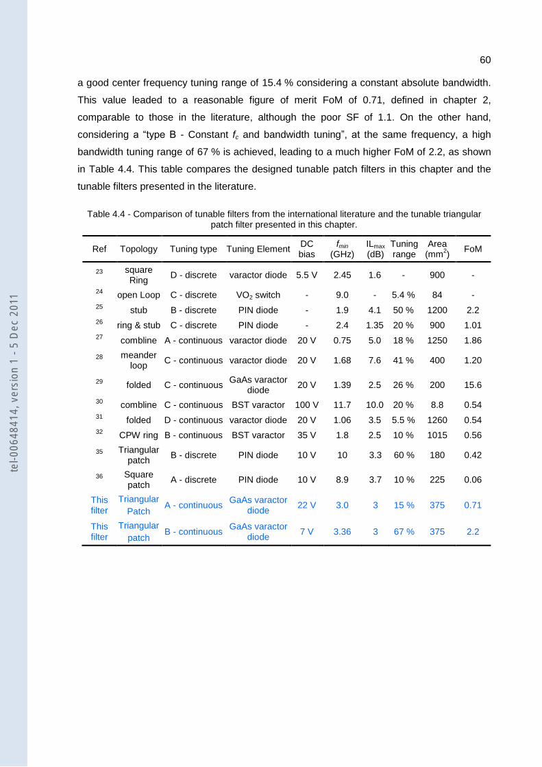
60
a good center frequency tuning range of 15.4 % considering a constant absolute bandwidth.
This value leaded to a reasonable figure of merit FoM of 0.71, defined in chapter 2,
comparable to those in the literature, although the poor SF of 1.1. On the other hand,
considering a “type B - Constant fc and bandwidth tuning”, at the same frequency, a high
bandwidth tuning range of 67 % is achieved, leading to a much higher FoM of 2.2, as shown
in Table 4.4. This table compares the designed tunable patch filters in this chapter and the
tunable filters presented in the literature.
Table 4.4 - Comparison of tunable filters from the international literature and the tunable triangular patch filter presented in this chapter.
Ref Topology Tuning type Tuning Element DC bias
fmin (GHz)
ILmax (dB)
Tuning range
Area (mm
2)
FoM
23
square Ring
D - discrete varactor diode 5.5 V 2.45 1.6 - 900 -
24 open Loop C - discrete VO2 switch - 9.0 - 5.4 % 84 -
25 stub B - discrete PIN diode - 1.9 4.1 50 % 1200 2.2
26 ring & stub C - discrete PIN diode - 2.4 1.35 20 % 900 1.01
27 combline A - continuous varactor diode 20 V 0.75 5.0 18 % 1250 1.86
28 meander
loop C - continuous varactor diode 20 V 1.68 7.6 41 % 400 1.20
29 folded C - continuous GaAs varactor
diode 20 V 1.39 2.5 26 % 200 15.6
30 combline C - continuous BST varactor 100 V 11.7 10.0 20 % 8.8 0.54
31 folded D - continuous varactor diode 20 V 1.06 3.5 5.5 % 1260 0.54
32 CPW ring B - continuous BST varactor 35 V 1.8 2.5 10 % 1015 0.56
35 Triangular
patch B - discrete PIN diode 10 V 10 3.3 60 % 180 0.42
36 Square patch
A - discrete PIN diode 10 V 8.9 3.7 10 % 225 0.06
This filter
Triangular
Patch A - continuous
GaAs varactor diode
22 V 3.0 3 15 % 375 0.71
This filter
Triangular
patch B - continuous
GaAs varactor diode
7 V 3.36 3 67 % 375 2.2
tel-0
0648
414,
ver
sion
1 -
5 D
ec 2
011

61
5 TUNABLE CIRCULAR PATCH FILTER WITH CENTER
FREQUENCY AND BANDWIDTH CONTROL
This chapter describes the design, fabrication, and measurement of a tunable filter
using a triple-mode circular patch resonator, initially centered at 2.45 GHz and with 27 % of
FBW3dB. The use of three modes allows the design of a bandpass patch filter with higher
level of miniaturization, a wider bandwidth, and low insertion loss. This topology was first
designed in my master’s dissertation as a fixed filter. Here, it was modified to tune
continuously its center frequency, bandwidth, and selectivity by varactor diodes. A detailed
study of the continuously tunable circular patch filter, its modeling, and the corresponding
analysis in terms of coupling scheme and coupling matrix are presented in this chapter.
5.1 INITIAL FILTER ANALYSIS
The basic triple-mode patch filter was designed with a circular resonator modified by
four radial slots. The three different resonant modes that form this filter are the two
fundamental degenerate modes (TMz1,1,0 - A and TMz
1,1,0 - B) and the second mode (TMz2,1,0).
The electric field patterns corresponding to these three modes are represented in Figure 41.
Figure 41 – Electric field patterns of the (a) fundamental degenerate mode TMz1,1,0 - A, (b)
fundamental degenerate mode TMz1,1,0 – B, and (c) second mode TM
z2,1,0 of a circular patch filter.
In a circular patch resonator, the patterns for the electric fields of the degenerate
fundamental modes are orthogonal as seen in Figure 41. Their corresponding current
distributions obtained from the EM simulations with the patch weakly coupled to the feed
lines are shown in Figure 42. Considering the feed lines positioned as in this figure, both
degenerate fundamental modes and the second mode are excited. This is because a
resonant mode is excited when the excitation port is positioned where the electric field
(a) (b) (c)
Max 0 Min
tel-0
0648
414,
ver
sion
1 -
5 D
ec 2
011

62
magnitude of this mode is not null. Therefore, considering the electric field patterns in Figure
41, it is clear that each port excites only one of the degenerate fundamental modes and both
ports excite the second mode. In the case where there is no perturbation in the patch
resonator, the EM simulations confirmed that TMz1,1,0 - A is excited only by the output,
resulting in the vertical current distribution presented in Figure 42(a). Analogously, the EM
simulations showed that TMz1,1,0 - B is excited only by the input, resulting in the horizontal
current distribution presented in Figure 42(b). TMz2,1,0, however, is excited by both ports,
resulting in the current distribution presented in Figure 42(c).
Figure 42 – Current distributions of the degenerate modes (a) TMz1,1,0 - A and (b) TM
z1,1,0 - B, and (c)
second mode TMz2,1,0 in an unperturbed circular patch resonator weakly coupled to the feed lines.
Nevertheless, the current distributions may rotate depending on the perturbation
inserted in the resonator. This rotation happens when using any type of radial slot positioned
at 45º away from the horizontal axis, as the ones illustrated in Figure 43.
Figure 43 - Layout of a circular patch resonator with four radial slots positioned at ±45⁰ from the
horizontal axis.
As an example, a small perturbation was added to the patch at 45º away from the
horizontal axis. This small perturbation in the form of a very thin rectangular slot rotates the
fields in the same way as the four slots in Figure 43, hardly changing the current distributions
of the modes. The rotated current distributions of the degenerate fundamental modes are
TMz1,1,0 - B TM
z1,1,0 - A
Input
Output
Input
Output
TMz2,1,0
Input
Output (a) (b) (c)
Input
A
A ’
Output
B
B’
Symmetry axis
tel-0
0648
414,
ver
sion
1 -
5 D
ec 2
011

63
shown in Figure 44. Note that the second mode does not rotate with the perturbation. Now
that degenerate modes are rotated, the feed lines are no longer positioned at their null
electric field, indicating that the degenerate modes are coupled to both ports. Considering the
symmetry axis of the structure relative to the input and output ports shown in Figure 43, one
can specify which modes have even or odd symmetry with respect to the symmetry axis of
this structure.
Figure 44 - Current distributions of the TMz1,1,0 degenerate (a) even and (b) odd modes and (c) TM
z2,1,0
mode in a slightly perturbed circular patch resonator weakly coupled to the feed lines.
Then, it is simple to observe that the slots A-A’ will mainly perturb the fundamental
even-mode, whereas the slots B-B’ will mainly perturb the fundamental odd-mode. The
TMz2,1,0 mode, however, will be perturbed by all the four slots, and thus, its frequency will
decrease more than the fundamental modes’ frequencies, leading to very close resonant
frequencies when the correct set of slots’ lengths is chosen.
Figure 45 shows the results of the EM simulations performed in Momentum using a
circular patch resonator with 8.1 mm of radius weakly coupled to the orthogonal feed lines as
shown in Figure 43. The substrate considered is the Rogers 3010 (εr = 10.2 and
thickness = 25 mils) without losses. From this figure, the initial dimensions of the slots were
chosen in order to split the degenerate modes, lower their resonant frequency, and lower the
second mode frequency so that the three resonant frequencies are around 2.4 GHz. The
feed lines were directly connected to the resonator to achieve the necessary couplings and
form the passband. Their width is 0.58 mm in order to match the 50 Ω characteristic
impedance microstrip line.
45⁰ small perturbation
TMz1,1,0
(b) (even mode)
TMz1,1,0
(a) (odd mode)
TMz2,1,0
(c) (odd mode)
tel-0
0648
414,
ver
sion
1 -
5 D
ec 2
011
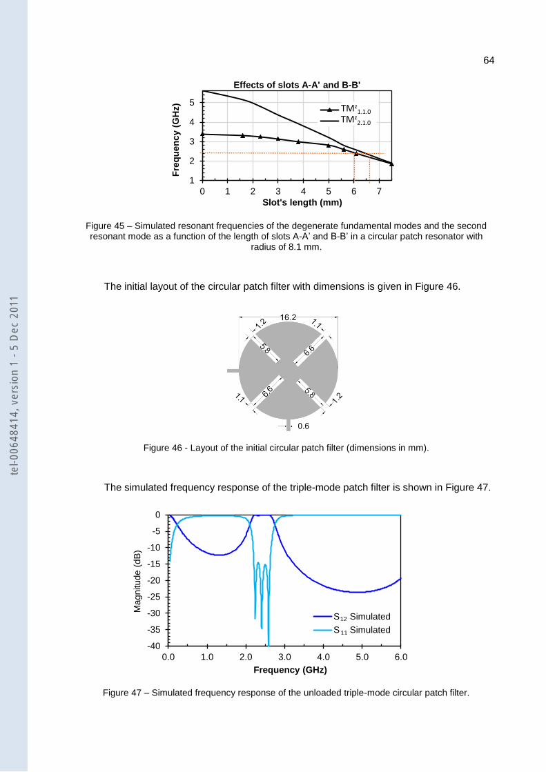
64
Figure 45 – Simulated resonant frequencies of the degenerate fundamental modes and the second resonant mode as a function of the length of slots A-A’ and B-B’ in a circular patch resonator with
radius of 8.1 mm.
The initial layout of the circular patch filter with dimensions is given in Figure 46.
Figure 46 - Layout of the initial circular patch filter (dimensions in mm).
The simulated frequency response of the triple-mode patch filter is shown in Figure 47.
Figure 47 – Simulated frequency response of the unloaded triple-mode circular patch filter.
1
2
3
4
5
0 1 2 3 4 5 6 7
Fre
qu
en
cy (
GH
z)
Slot's length (mm)
Effects of slots A-A' and B-B'
TMz2,1,0
TMz1,1,0
-40
-35
-30
-25
-20
-15
-10
-5
0
0.0 1.0 2.0 3.0 4.0 5.0 6.0
Magnitude (
dB
)
Frequency (GHz)
S Simulated
S Simulated
12
11
tel-0
0648
414,
ver
sion
1 -
5 D
ec 2
011

65
The filter exhibits a central frequency of 2.43 GHz and FBW3dB of 28 %. The EM
simulations showed that the pole at the lowest frequency in Figure 47 corresponds to the
TMz1,1,0 odd mode, the pole in the middle corresponds to the TMz
1,1,0 even mode, and the
pole at higher frequency corresponds to TMz2,1,0.
The conventional coupling scheme of a circular patch topology using only the
degenerate modes is shown in Figure 48(a). Note that one degenerate mode is only coupled
to the source and the other, to the load, as shown in the beginning of this chapter for a
circular patch resonator without perturbation. Due to the symmetric geometry of the filter, the
behavior of the degenerate fundamental modes in this structure can be interpreted with a 45º
rotation that remodels the couplings between the nodes, as shown in Figure 48(b). In the
second case, each mode is connected to both ports. These schemes are mathematically
equivalent, however, as explained, the current distribution indicates that the second scheme
better represents the model of this filter.
Figure 48 – (a) Conventional coupling scheme of the degenerate modes in a circular patch resonator. (b) Interpretation of the coupling scheme of the degenerate modes for the patch filter under analysis.
Figure 49 presents the complete coupling scheme for the triple-mode circular patch
filter discussed in this chapter.
Figure 49 – Complete coupling scheme of the circular patch filter with one single (triple-mode) resonator supporting the two fundamental degenerate modes and the second mode.
Dual-mode resonator
S L
1
2
(a)
S
L
1
2
(b)
Triple-mode resonator
MS1 M1L
MS2 M2L
MSL S L
1
2
Odd-mode
Even-mode
3
MS3 M3L
Odd-mode
tel-0
0648
414,
ver
sion
1 -
5 D
ec 2
011

66
In Figure 49, “1”, “2”, and “3” were chosen to represent the fundamental split odd
mode, the fundamental split even mode, and the second mode, respectively. Thus, MS1 = -
M1L, MS2 = M2L and MS3 = -M3L. The coupling matrix related to the coupling scheme presented
in this figure is given by MO in (42), where the index “O” was used to refer to the circular
resonator.
[
]
(42)
Initially, there is no evidence concerning the coupling between source and load as they
are directly connected to the resonator and there are no TZ in the frequency response of the
filter. Because of that, the initial choice of MSL will be zero. Using such configuration, the
coupling matrix can be analytically calculated54 considering the equations given in section 3.1
and an in-band return loss of 15 dB, resulting in matrix (43).
[
]
(43)
It is important to notice that the position of each mode and its related couplings is
merely a choice when building the matrix. For example, in matrix (43), “1” and “2” were
chosen to represent the fundamental odd (in blue) and even (in red) modes, respectively.
However, “1” and “2” could be chosen to represent the opposite, the even and odd modes. In
the latter case, the matrix should be changed as shown in matrix (44) in order to keep the
same couplings and to produce exactly the same response.
[
]
(44)
To facilitate the comprehension, the first choice was used in this analysis, where M11,
M22 and M33 represent each mode from the lower to the highest resonant frequency,
indicated by the three poles in the frequency response of the filter, shown in Figure 47.
Figure 50 compares the theoretical frequency response produced by matrices (43) (or
(44) considering the filter centered at 2.43 GHz and bandwidth of 650 MHz, and the EM
tel-0
0648
414,
ver
sion
1 -
5 D
ec 2
011

67
simulation result of the filter without tuning elements. It can be seen at the inset of this figure
that the insertion loss is almost zero, presenting a small ripple of 0.2 dB within the passband,
indicating that the radiation loss is negligible due to the nature of the feed lines coupling to
the resonator. All curves are in very good agreement except for the lower rejection band. The
theoretical curve has better rejection than the simulated one because the input and output
are directly connected to the resonator. When the feed lines are connected in such manner,
the filter acts as a low-pass filter from DC to low frequencies, which is not accounted for in
the matrix elements. The matrix models only the filter passband and a narrow frequency
range around it. The matrix can model neither the filter response at very low frequencies nor
the filter spurious harmonics.
Figure 50 – Lossless simulated and theoretical (from matrix MO in (43)) responses of the unloaded triple-mode circular patch filter. An inset of the passband is shown on the upper right corner.
5.2 TUNING ANALYSIS
In order to verify how a patch filter behaves when capacitively loaded, the proposed
patch filter was analyzed with capacitances across its slots at three possible positions:
outside edge, middle or inside edge of the slots, as seen in Figure 51.
Figure 51 – Patch filter capacitively loaded at the (a) outside edge of the slots, (b) middle of the slots, and (c) inside edge of the slots.
-40
-35
-30
-25
-20
-15
-10
-5
0
0.0 1.0 2.0 3.0 4.0 5.0 6.0
Magnitude (
dB
)
Frequency (GHz)
S21 Theory S11 Theory S21 Simulated S11 Simulated
(a) (b) (c)
S S S
-2
-1
0
1.8 2.3 2.8
tel-0
0648
414,
ver
sion
1 -
5 D
ec 2
011

68
The simulation results showed that each capacitance affects more than one resonant
mode. This was expected as the simulations showed that one slot affects more than one
mode, which is further detailed below.
Once more, the change in modal frequencies is affected not only by the capacitances,
but also by their position across the slots. Table 5.1 shows the influence of the capacitances
position on the tuning range, considering the filter frequency response with RL better than
10 dB within the passband. The IL remained practically constant and null along the whole
tuning range. The four capacitances were kept equal in order to simplify the study. At a
specific capacitance (CS), the modes superimpose destructively at the resonant frequency
(fS) highly increasing the insertion loss. By further increasing the capacitances, the insertion
loss decreases to its initial value up to a capacitance (Cmax) in which the RL becomes worse
than 10 dB due to the mismatch of the resonator impedance. In this table, the maximum
tuning range is considered up to the capacitance Cmax, which depends on its position at the
slots. Cmax is equal to 5.5 pF when the capacitances are positioned at the inside edge of the
slots, 4.4 pF in the middle, and 2.67 pF when positioned at the outside edge of the slots.
Table 5.1 – Simulated center frequency and capacitance ranges for different positions of capacitances along the four slots of the circular patch filter.
Capacitance position Capacitance range
(pF) Frequency range
(GHz) CS
(pF) fS
(GHz) Tuning range
(%)
Inside edge of slots 0 – 5.50 2.43 – 1.88 8.7 1.82 25 (max. range)
Middle of slots 0 – 4.40 2.43 – 1.49 2.00 1.82 48 (max. range)
0 – 1.75 2.43 – 1.88 - - 25
Outside edge of slots 0 – 2.67 2.43 – 1.54 1.33 1.82 45 (max. range)
0 – 1.16 2.43 – 1.88 - - 25
The simulated results in this table show that a maximum center frequency tuning range
of 48 % is obtained when the capacitances are positioned in the middle of the slots, which is
the broadest tuning range of the three positions. In order to compare the influence of the
capacitances in the center frequency response, the capacitances were also assessed within
the same tuning range of 25 % from 2.43 GHz to 1.88 GHz at the three positions. Table 5.1
shows that for this range, a broader capacitance variation is needed when the capacitances
are placed at the inside edge of the slots. This is understandable because at this position,
the capacitances are short-circuited by the end of the slot, and hence their effect is weak.
Therefore, for a given loading capacitance, the sensitivity of the resonance frequency
increases when the capacitances are moved towards the border of the resonator.
Although the frequency range obtained with the capacitances positioned at the border
of the resonator is close to the one with the capacitances in the middle of slots, its
tel-0
0648
414,
ver
sion
1 -
5 D
ec 2
011

69
capacitance range is much narrower, making the filter excessively sensitive and, as
explained before, more sensible to the parasitic resistance when considering a real tuning
element. Therefore, the filter was designed with capacitors in the middle of the slots,
providing the largest tuning range with a well-matched response within a reasonable range of
capacitance.
For a proof-of-concept of this initial study, a circular filter was fabricated using fixed
capacitors across the four slots, with the layout presented in Figure 52. The capacitors used
were SMD 0505 capacitors, modeled as a series RLC with R = 0.5 Ω, and L = 0.3 nH. The
filter was fabricated with traditional photolithographic process, which brought some
inaccuracies in the whole filter dimensions, slightly changing its frequency response. Thus,
after the fabrication, the filter was measured and its real dimensions were used in the filter
simulations.
Figure 52 – Picture of the prototype circular patch filter with capacitors across the four slots.
The simulated and measured frequency responses of the unloaded filter, shown in
Figure 53, are in very good agreement. The triple-mode patch filter is centered at 2.37 GHz,
with FBW3dB of 28 %, insertion loss lower than 0.7 dB and return loss better than 12 dB.
Figure 53 – Simulated and measured frequency responses of the unloaded triple-mode circular patch filter.
tel-0
0648
414,
ver
sion
1 -
5 D
ec 2
011

70
The patch filter could be tuned by manually changing the capacitors. The capacitance
variation from zero to 1.8 pF resulted in 25 % of center frequency tuning range, varying from
2.37 GHz to 1.8 GHz. At the same time, the filter’s passband decreased from 28 % to 8 % for
the same range of capacitances. These results are summarized in Table 5.2 and presented
in Figure 54.
Table 5.2 – Experimental results of the patch filter loaded with four equal capacitors mounted in the middle of the slots with different capacitances.
Value of each capacitor (pF) Center frequency (GHz) FBW3dB (%)
No capacitors 2.37 27.6
0.3 2.30 24.3
0.5 2.21 23.0
0.7 2.15 22.7
1.2 1.91 17.2
1.5 1.92 9.8
1.8 1.84 8.1
Figure 54 - Measured frequency responses of the circular patch filter loaded at the middle of the four slots with different capacitor values.
-45
-40
-35
-30
-25
-20
-15
-10
-5
0
1.0 1.5 2.0 2.5 3.0 3.5 4.0 4.5 5.0
Insert
ion L
oss (
dB
)
Frequency (GHz)
no cap
c=0.3 pF
c=0.5 pF
c=0.7 pF
c=1.2 pF
c=1.5 pF
c=1.8 pF
-35
-30
-25
-20
-15
-10
-5
0
1.0 1.5 2.0 2.5 3.0 3.5 4.0 4.5 5.0
Retu
rn L
oss (
dB
)
Frequency (GHz)
no cap
c=0.3 pF
c=0.5 pF
c=0.7 pF
c=1.2 pF
c=1.5 pF
c=1.8 pF
tel-0
0648
414,
ver
sion
1 -
5 D
ec 2
011

71
When the capacitances are greater than 1.8 pF, the passband characteristic is
deformed and thus, the results were disregarded. The results presented consider an
insertion loss better than 1.3 dB and a return loss better than 13 dB.
In order to obtain an electronically tuning, the filter was then analyzed considering the
same varactor diode used in the design of the triangular patch resonator, the diode
MA46H71, from M/A-COM. The varactor model has been detailed in section 4.3. The same
back-to-back configuration was used because it facilitates the diodes biasing, halves the total
capacitance, improves the linearity performance, and better adjusts the capacitance of the
tuning filter.
In the circular patch filter, as the input and output are directly connected to the
resonator, the biasing configuration was inverted, and the patch resonator was connected to
a positive DC bias source, instead of connected to the ground, as shown in Figure 55.
Figure 55 - Back-to-back configuration of the varactor diodes to halve the capacitance and improve linearity.
5.3 THEORETICAL ANALYSIS & COMPLETE SIMULATIONS
As the couplings in this circular patch filter are not as simple as in the previous
triangular filter, some investigations were carried out to further understand their behavior.
The initial studies with fixed capacitors indicated that the simulations give a very good
prediction of the filter response. The circular patch filter was then analyzed with a more
complete model, using the varactor diode model positioned in the middle of the slots in the
back-to-back configuration presented in Figure 55.
Four strips parallel to each slot were added to the layout, providing an easy access for
the varactor diodes to the ground through the edges of the substrate board, and keeping the
layout simple without any vias, resulting in the filter layout shown in Figure 56. Simulations of
the filter with these strips showed that they have almost no effect on the filter response,
slightly altering the scattering parameters in frequencies higher than 3 GHz.
R
V
V
tel-0
0648
414,
ver
sion
1 -
5 D
ec 2
011

72
Figure 56 – Topology of the triple-mode circular bandpass patch filter with tuning elements in the middle of each slot.
The coupling matrix was recalculated with an in-band return loss of 10 dB within the
passband, resulting in the coupling matrix presented by (45).
[
]
(45)
The substrate considered in the simulations and used to realize the filter is the Rogers
3010 (εr = 10.2, tan δ = 0.0023 and thickness = 25 mils). The simulations were carried out
considering the substrate dielectric and conductor losses, which individual effects in the
insertion loss of the filter passband is shown in Figure 57. The conductor and dielectric
losses are in the same order of magnitude. For comparison, the filter was also simulated with
a substrate with five times higher dielectric loss (tan δ = 0.016), like the low-cost FR4
substrate. This leads to an increase in the insertion loss from 0.4 dB to 2 dB.
Figure 57 – Individual and total effects of the dielectric and conductor losses in the passband of the circular patch filter.
-3
-2.5
-2
-1.5
-1
-0.5
0
2.0 2.2 2.4 2.6 2.8
Magnitude (
dB
)
Frequency (GHz)
No loss
Dielectric Loss (tan = 0.0023)
Conductor Loss
Dielectric+Conductor Losses
Dielectric Loss (tan = 0.016)
C
A
CC
CB
A B
C D CD
R
V V
tel-0
0648
414,
ver
sion
1 -
5 D
ec 2
011

73
Figure 58 shows the theoretical frequency response considering the filter centered at
2.41 GHz and with 650 MHz of bandwidth, the simulated, and the measured frequency
responses of the unloaded circular patch filter. The theoretical curves consider an ideal
resonator with infinite unloaded quality factor Qu, seen in the inset in Figure 58, which agreed
well with the lossless simulations.
Figure 58 – Measured, simulated and theoretical (from matrix MO in (45)) frequency responses of the unloaded triple-mode circular patch filter. An inset of the passband is shown on the upper right corner.
This new study is concerned with how the capacitance connected to each slot affects
the coupling coefficients of the matrix (45). A comparison between the simulated and
theoretical frequency responses was carried out by varying the capacitance of only one slot
at a time.
In order to clarify the study, the capacitance in each slot will be referenced as CA, CB,
CC and CD, respectively, as illustrated in Figure 56 and the frequency of the resonant modes
TMz1,1,0 odd, TMz
1,1,0 even, and TMz2,1,0 will be referred as f1, f2, and f3, respectively. All
theoretical curves ware plotted with the center frequency and bandwidth of the unloaded
circular patch filter.
5.3.1 EFFECT OF CA AND CC ON THE COUPLING COEFFICIENTS
CA and CC have the same effect on the response of the filter, due to its symmetry. If
these two capacitances are changed separately, the filter cannot be matched and the return
loss is not acceptable. Therefore, the analysis was carried out with the influence of equal
capacitances CA and CC varying together.
-50
-45
-40
-35
-30
-25
-20
-15
-10
-5
0
1.5 2.0 2.5 3.0 3.5
Magnitude (
dB
)
Frequency (GHz)
MeasurementSimulationTheory
-3
-2
-1
0
1.5 2.0 2.5 3.0 3.5
tel-0
0648
414,
ver
sion
1 -
5 D
ec 2
011

74
From the increase of these two capacitances, one can perceive two different effects in
the mode frequencies: the decrease of f2 approximating it to f1, and the decrease of f3. Each
one of these effects can be individually modeled by increasing M22 and M33. It is interesting to
note that both coefficients vary by the same amount of w, added to the coupling matrix in
(46).
[
]
(46)
Figure 59 shows the simulated frequency responses when varying both CA and CC with
the same values and the corresponding theoretical frequency responses for different values
of w, modeled by matrix MAC in (46). Note that a very small capacitance already brings f2 so
close to f1 that it is not possible to distinguish each other anymore.
Figure 59 – Simulated frequency responses of the triple-mode circular patch filter capacitively loaded at slot A and slot C (dotted-line), and respective theoretical curves according to matrix MAC in (46) (full-
line).
In conclusion, the main effect of increasing CA and CC is to increase both M22 and M33,
which is equivalent to reduce both f2 and f3.
5.3.2 EFFECT OF CB ON THE COUPLING COEFFICIENTS
A different behavior can be seen when changing CB. The increase of this capacitance
lowers both f1 and f3 at the same time, while slightly increasing f2. Simulations showed that
CB has a stronger effect on f3 than on f1, reducing f3 more than f1. Thus, to accurately model
this influence, M33 should increase more than M11. From the analysis of the coupling matrix, it
-45
-40
-35
-30
-25
-20
-15
-10
-5
0
1.5 2.0 2.5 3.0 3.5
Magnitude (
dB
)
Frequency (GHz)
Variation in CA and CC
Theory Simulation
CA=CC (pF) w 0.02 0.055 0.06 0.097 0.11 0.165
tel-0
0648
414,
ver
sion
1 -
5 D
ec 2
011

75
was possible to determine the correct amount: M33 should be increased 2.4 times more than
M11, resulting in the coupling matrix MB in (47). Using these values, the theoretical responses
were correctly fitted to the simulations shown in Figure 60. Even though there is a small
change in f2, M22 was not changed because the change in M11 and M33 resulted in the
expected variation of f2.
[
]
(47)
Figure 60 – Simulated frequency responses of the triple-mode circular patch filter capacitively loaded only at slot B (dotted-line), and respective theoretical curves according to matrix MB in (47) (full-line).
In conclusion, the main effect of increasing CB is to increase both M11 and M33, which is
equivalent to reduce both f1 and f3, and slightly increase f2.
5.3.3 EFFECT OF CD ON THE COUPLING COEFFICIENTS
CD affects the filter response in yet another way. The analysis of the effect of CD is
much more complex because this capacitance affects several couplings at the same time.
Initially, by increasing CD, f1 and f3 decrease, and f2 remains unchanged. As seen in the
previous section concerning the effect of CB, when M11 and M33 increase, f1 and f3, are
reduced, but f2 is slightly increased, even if M22 remains unchanged. Therefore, in the case of
CD, if M11 and M33 increase, M22 has to slightly increase, in order to lower f2 and keep it at the
same frequency. This situation can be simply modeled by increasing the three susceptances
by the same amount.
-50
-40
-30
-20
-10
0
1.5 2.0 2.5 3.0 3.5
Magnitude (
dB
)
Frequency (GHz)
Theory Simulation
CB (pF) z 0.158 0.038 0.368 0.085 0.632 0.139
Variation in CB
tel-0
0648
414,
ver
sion
1 -
5 D
ec 2
011

76
The EM simulations, however, also exhibited a transmission zero (TZ) at the upper side
of the passband. Increasing CD lowers the frequency at which the TZ is located. This was
expected because CD makes a quasi-direct path between input and output ports. A
transmission zero can be modeled by any coupling that provides a shorter path for the signal
from the input to the output. A TZ cannot be modeled by susceptances, because they only
model changes in the resonant modes frequency. Thus, it is necessary to find which coupling
or couplings provide the expected TZ. An inspection of the coupling coefficients MS1 (= -M1L),
MS2 (= M2L), MS3 (= -M3L), and MSL (= MLS) showed the following:
(1) by increasing the coupling between the feed lines and the fundamental even
mode MS2, two TZ are brought to finite frequencies, one at each side of the filter
bandpass. If these couplings are decreased, the overall rejection of the out-of-
band frequency response worsens;
(2) by decreasing the coupling between the feed lines and the fundamental odd
mode MS1, one TZ is brought to finite frequencies below the filter bandpass. If
these couplings are increased, the overall rejection of the out-of-band frequency
response worsens;
(3) by decreasing the coupling between the feed lines and the TMz2,1,0 mode
MS3, one TZ is brought to finite frequencies at the upper side of the filter
bandpass. If these couplings are increased, the overall rejection of the out-of-
band frequency response worsens;
(4) by increasing the coupling between source and load MSL, a TZ is brought to
finite frequencies below the filter bandpass. If this coupling is decreased, the TZ
is moved to the upper side of the filter bandpass.
Thus, the TZ at the upper side of the filter bandpass can be modeled by decreasing
either MS3 (= -M3L), or MSL (= MLS), or both. Nevertheless, those couplings also change the
frequency of all resonant modes. Therefore, the initial scenario where all susceptances could
be increased of the same amount to model an increase in CD is no longer valid. The
susceptances will increase, but with different amounts a, b and c. The corresponding matrix
for modeling the effect of CD is finally given by MD, in (48).
[
]
(48)
The frequency response resulted from this matrix for different values of a, b, c, g and u
is presented in Figure 61 with the respective simulated curves obtained by varying CD. As
tel-0
0648
414,
ver
sion
1 -
5 D
ec 2
011

77
can be seen in Figure 61, the filter response was very well modeled by changing the three
susceptances and both couplings MS3 (= -M3L), and MSL (= MLS).
Figure 61 – Simulated frequency responses of the triple-mode circular patch filter capacitively loaded only at slot D (dotted-line), and respective theoretical curves according to matrix MD in (48) (full-line).
In conclusion, the effect of increasing CD is to increase the three susceptances and the
magnitude of MS3 and MSL, which is equivalent to reduce both f1 and f3, while keeping f2
unchanged, and to bring a transmission zero closer to the upper side of the passband,
improving the selectivity at the upper side of the filter passband.
5.3.4 COMBINED EFFECT OF THE 4 CAPACITANCES ON THE COUPLING COEFFICIENTS
The study carried out in the above sub-sections has shown that when using the
capacitances across the four slots, the coupling coefficients varied in different ways, allowing
this patch filter to be reconfigured by varactor diodes in terms of its center frequency,
bandwidth, and rejection. The rejection is changed by bringing a transmission zero close to
the upper side of the passband. Particularly for the susceptances, they all increased with the
increase of each individual capacitance, and thus, the result of increasing all capacitances
together is obviously a simultaneous decrease in the frequency of the three resonant modes.
Furthermore, important observations can be done from the theoretical analysis of different
filter responses, analogously to the triangular filter:
M11 changes the fundamental odd-mode, M22 changes the fundamental even-
mode, and M33 changes the second odd-mode. If individual capacitances can
also change individually these modes, a tunable filter with independent tuning of
frequency and bandwidth is feasible.
-45
-40
-35
-30
-25
-20
-15
-10
-5
0
1.5 2.0 2.5 3.0
Magnitude (
dB
)
Frequency (GHz)
Theory Simulation
a b c g u 0.10 0.14 0.23 -0.05 1.00 0.20 0.10 0.37 -0.12 0.73 0.34 0.06 0.50 -0.12 0.51
Variation in CD
tel-0
0648
414,
ver
sion
1 -
5 D
ec 2
011

78
The center frequency is a linear function of the average susceptance
(M11 + M22 + M33)/3, as seen in Figure 62(a). Figure 62 was plotted with the
coupling coefficient values adjusted to the simulations (and later to
measurements with the varactor diodes) of equal capacitances at the four slots
of the filter.
FBW3dB is a linear function of (M33 - M11), corresponding to the difference
between the maximum and minimum susceptances, as seen in Figure 62(b).
Figure 62 – Simulated and theoretical curves of the filter loaded with equal capacitances at the four slots (a) center frequency x capacitance (full-line), center frequency x average susceptance (dashed-
line); (b) bandwidth x capacitance (full-line), bandwidth x (M33-M11) (dashed-line).
The analysis of the capacitance effect in each slot showed that individual changes in
each mode frequency are not possible, so the degree of freedom of this filter is reduced
compared to the tunable triangular patch filter.
On the other hand, simulations with equal capacitances at the four slots showed that
both frequency and bandwidth decrease at the same time when increasing all the
capacitances. In terms of the coupling matrix analysis, the coupling coefficients that generate
the theoretical curves corresponding to those simulations are presented in Figure 63.
Figure 63 – Couplings coefficients (M11, M22, M33 and MSL) variation corresponding to the simulated results of the filter loaded with equal capacitances at the four slots.
-0.1
0.1
0.3
0.5
0.7
0.9
1.1
1.3
0
0.2
0.4
0.6
0.8
1
1.2
1.4
1.6
1.8 1.9 2 2.1 2.2 2.3 2.4 2.5
Capacitance (
pF
)
Frequency (GHz) (a)
Av
era
ge
Su
scep
tan
ce
-1.8
-1.6
-1.4
-1.2
-1.0
0
0.2
0.4
0.6
0.8
1
10 15 20 25 30
Capacitance (
pF
)
FBW3dB (%)
M33 - M
11
(b)
-1.0
-0.5
0.0
0.5
1.0
1.5
2.0
0 0.25 0.5 0.75 1 1.25 1.5
Couplin
g C
oeff
icie
nt
Capacitance (pF)
M11
M22
M33
MSL
11
22
33
SL
tel-0
0648
414,
ver
sion
1 -
5 D
ec 2
011

79
The coupling matrix analysis showed that the susceptance M33 increases more than
M11 or M22 because of the combined effect of the capacitances. This means that f3 decreases
faster than the two other frequencies, explaining the reduction of the filter center frequency
and bandwidth.
Furthermore, the simulations with equal capacitances at the four slots, in Figure 64
showed that a transmission zero is brought to the upper side of the passband. The
capacitance given in the legend of these curves is the total capacitance of the back-to-back
varactor diodes configuration connected to each slot.
Figure 64 – Simulated frequency responses of the circular patch filter loaded equally at the four slots as illustrated in Figure 56. The value is the total capacitance of the two varactor diodes in each slot.
(a) Insertion loss. (b) Return loss.
As explained in section 5.3.3 concerning the effect of CD, the transmission zero was
accounted for by the negative coupling between the input and output MSL = MLS, and a small
modification of the coupling between source/load and resonant mode “3” MS3 = -M3L. The
theoretical curves are presented in Figure 65, which considered the combined effects of the
-45
-40
-35
-30
-25
-20
-15
-10
-5
0
1.0 1.5 2.0 2.5 3.0 3.5 4.0 4.5 5.0
Insert
ion L
oss (
dB
)
Frequency (GHz)
Cj = 0 pF
Cj = 0.2 pF
Cj = 0.24 pF
Cj = 0.34 pF
Cj = 0.47 pF
Cj = 0.6 pF
Cj = 0.75 pF
Cj = 0.8 pF
Simulation
(a)
-45
-40
-35
-30
-25
-20
-15
-10
-5
0
1.0 1.5 2.0 2.5 3.0 3.5 4.0 4.5 5.0
Retu
rn L
oss (
dB
)
Frequency (GHz)
Cj = 0 pF
Cj = 0.2 pF
Cj = 0.24 pF
Cj = 0.34 pF
Cj = 0.47 pF
Cj = 0.6 pF
Cj = 0.75 pF
Cj = 0.8 pF
Simulation
(b)
tel-0
0648
414,
ver
sion
1 -
5 D
ec 2
011

80
coupling coefficients corresponding to the effect of the four equal capacitances used in the
simulations. The values of the coupling coefficients of these curves can be extracted from
Figure 63.
Figure 65 – Theoretical response of the circular patch filter loaded equally at the four slots, with the coefficients presented in Figure 63. (a) Insertion loss. (b) Return loss.
5.4 TUNABLE FILTER FABRICATION AND MEASUREMENTS
5.4.1 SMALL-SIGNAL MEASUREMENT
The fabricated and assembled tunable bandpass circular patch filter is presented in
Figure 66. The configuration of the patch filter with the input and output directly connected to
the resonator provides a DC path, which deteriorates the filter rejection at very low
frequencies, as explained above. In order to enhance the filter rejection at low frequencies, a
decoupling capacitor was used at the input and output feed lines. The filter was assembled
with all the varactor diodes biased by a single DC voltage connected to the patch through a
47 KΩ resistor to block the RF signal.
-50
-40
-30
-20
-10
0
1.5 2.0 2.5 3.0 3.5
Insert
ion L
oss (
dB
)
Frequency (GHz) (a)
-50
-40
-30
-20
-10
0
1.5 2.0 2.5 3.0 3.5
Retu
rn L
oss (
dB
)
Frequency (GHz) (b)
tel-0
0648
414,
ver
sion
1 -
5 D
ec 2
011

81
Figure 66 – (a) Fabricated circular patch filter without tuning elements. (b) Assembled tunable bandpass circular patch filter beside of a 2 € cents piece.
The center frequency of the patch filter could be continuously tuned from 1.8 GHz to
2.35 GHz, which represents a tuning range of 27 % with a DC bias voltage ranging from
0.5 V to 20 V. This is equivalent to the total capacitance of the back-to-back configuration
varying from 0.2 pF to 0.8 pF. Within this range, the results showed good performance with
the insertion loss lower than 2.8 dB and return loss better than 11 dB.
Nonetheless, a more rigorous limit could be set to a maximum IL of 2 dB and RL of
13 dB, reducing the tuning range from 2 GHz to 2.35 GHz (16 % of tuning range). These
measured results are shown in Figure 68. It can be seen that the measurements are in very
good agreement with the simulated results and the theoretical curves in Figure 64 and Figure
65, respectively. As expected, at the same time, the filter FBW3dB could be changed from 9 %
to 26 %
Figure 67 – Measured frequency response (insertion loss) of the tunable circular patch filter with a single DC bias applied to all varactors from 1 V to 20 V.
-45
-40
-35
-30
-25
-20
-15
-10
-5
0
1.0 2.0 3.0 4.0 5.0 6.0
Insert
ion L
oss (
dB
)
Frequency (GHz)
No varactorbias=20 Vbias=9 Vbias=5 Vbias=3 Vbias=2 Vbias=1.5 Vbias=1 V
tel-0
0648
414,
ver
sion
1 -
5 D
ec 2
011

82
Figure 68 – Measured frequency response (return loss) of the tunable circular patch filter with a single DC bias applied to all varactors from 1 V to 20 V.
5.4.2 NONLINEAR MEASUREMENTS
5.4.2.1 1-dB Compression Point (P1dB)
The 1-dB compression point (P1dB) specified at the input of the filter was measured at
the center frequency for different low biasing conditions, presented in Table 4.2. For DC bias
voltages higher than 2 V, the maximum input power allowed by the setup (+21.4 dBm) was
reached, and the output had not yet been compressed thus, the measurement could not be
done. The important fact is that the filter is easily capable of handle +10 dBm of power, even
at low bias voltage, suitable to most communication systems. If a tunable working frequency
comprised between 2 GHz and 2.35 GHz is considered, then the P1dB is better than
+18.8 dBm, the insertion is lower than 2 dB, and the return loss is better than 13 dB, making
this kind of tunable filter very efficient.
Table 5.3 - P1dB of the tunable circular filter for different biasing conditions.
Center Frequency (GHz) Bias Voltage (V) P1dB (dBm)
1.95 1.0 +12.9
1.98 1.5 +15.7
2.0 2.0 +18.8
>2.0 >2.0 > +18.8
-45
-40
-35
-30
-25
-20
-15
-10
-5
0
1.0 2.0 3.0 4.0 5.0 6.0
Retu
rn L
oss (
dB
)
Frequency (GHz)
No varactor
bias=20 V
bias=9 V
bias=5 V
bias=3 V
bias=2 V
bias=1.5 V
bias=1 V
tel-0
0648
414,
ver
sion
1 -
5 D
ec 2
011

83
5.4.2.2 Third-order Intercept Point
Two tones separated by ∆f = 5 MHz were positioned within the bandwidth of the filter,
tuned to very low bias voltage with the measurement setup shown in Figure 11. The tones
were delivered to the filter with power level from -20 dBm to -1.6 dBm. The level of input
tones and the 3rd order intermodulation components were measured at the filter output and
were used to calculate the 3rd order intercept point (IIP3) of the filter referred to the input port.
The minimum IIP3 was found to be of +25.8 dBm for the 175 MHz-bandwidth filter
centered at 1.95 GHz as shown in Table 4.3. As expected, this value improves for higher
bias voltages and center frequencies. The IIP3 is greater than +31 dBm when the center
frequency is higher than 2 GHz.
Table 5.4 – Measured IIP3 of the tunable filter with varactor diodes in back-to-back configuration.
Center Frequency (GHz) Bias Voltage (V) IP3 (dBm)
1.95 1.0 +25.8
1.98 1.5 +29.5
2.0 2.0 +31.3
5.5 EXTENDED ANALYSIS OF THE COUPLING MATRIX
The bias configuration using only one voltage is very simple, although it limits the
degree of freedom related to the control of the resonant modes. Independent bias voltages
for each varactor diode (except for CA and CC, which should always act as matched pair,
being changed together) leads to a higher degree of freedom because more configurations of
center frequency and bandwidths can be chosen. A further analysis of the coupling matrix of
this filter leads to some considerations about using this circular patch filter to obtain a tunable
filter with constant bandwidth or a tunable filter with constant frequency.
As the bandwidth of this filter is determined by (M33 – M11), if this difference is kept
constant, filters with the same fractional bandwidth at different frequencies can be designed.
It is important to remind, that even if M22 does not affect directly the width of the passband, it
should be also changed in a manner that its frequency remains between the two other
frequencies otherwise the passband characteristic will change. Thus, for keeping the
bandwidth constant, M11 and M33 should change in the same direction and by the same
amount z. M22 should also change in the same direction and by an amount, ideally the same
as the others, as shown in Figure 69, as a response for the matrix (49), but it is not
obligatory. The study of the effects of each capacitance in the filter response presented in
tel-0
0648
414,
ver
sion
1 -
5 D
ec 2
011

84
section 5.3 showed that CB changes both M11 and M33. On the other hand, CA and CC change
both M22 and M33. With the combination of these capacitances, M33 always changes more
than M11, and therefore, a constant fractional bandwidth is not possible for this filter, even
with the use of multiple bias voltages. Therefore, the filter response presented in Figure 69
cannot be obtained experimentally.
[
]
(49)
Figure 69 – Theoretical responses for different center frequencies with the same fractional bandwidth.
On the other hand, keeping a constant center frequency and varying the bandwidth can
be achieved by changing both M11 and M33 in the opposite direction, keeping the condition
(M11 + M33 + M22)/3 constant. A basic example is given by matrix (50), with the theoretical
curves presented in Figure 70. Again, from the study presented in section 5.3, it was shown
that CB changes both M11 and M33, and CA and CC change both M22 and M33. Therefore, a
tunable bandwidth filter with constant center frequency is feasible with the use of two bias
voltages, one to control CB and another one to control CA and CC in opposite ways. For that,
the CB bias voltage should increase while decreasing CA and CC bias voltage (or vice-versa),
without any capacitance at slot D.
[
]
(50)
-45
-40
-35
-30
-25
-20
-15
-10
-5
0
1.5 2.0 2.5 3.0 3.5
Magnitude (
dB
)
Frequency (GHz)
z = 1
z = 0
z = -1
tel-0
0648
414,
ver
sion
1 -
5 D
ec 2
011
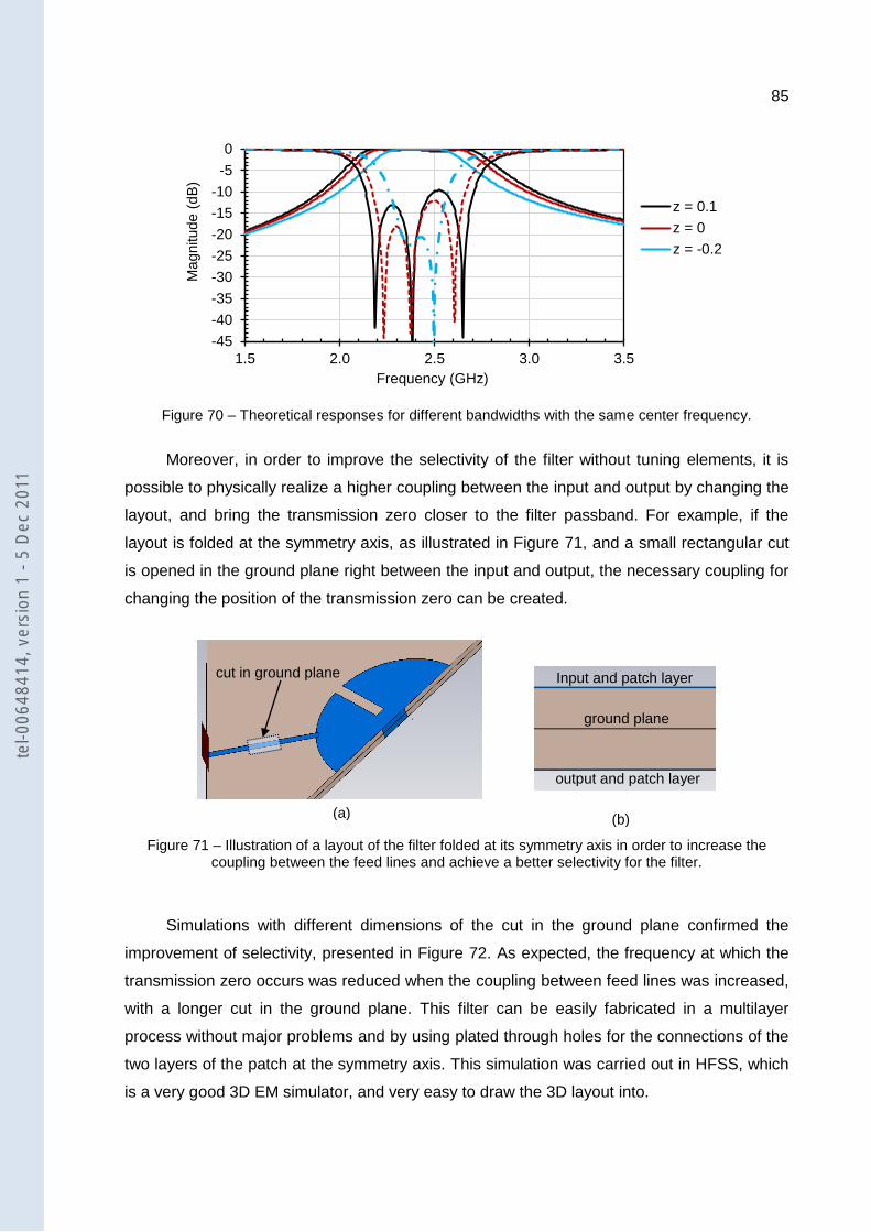
85
Figure 70 – Theoretical responses for different bandwidths with the same center frequency.
Moreover, in order to improve the selectivity of the filter without tuning elements, it is
possible to physically realize a higher coupling between the input and output by changing the
layout, and bring the transmission zero closer to the filter passband. For example, if the
layout is folded at the symmetry axis, as illustrated in Figure 71, and a small rectangular cut
is opened in the ground plane right between the input and output, the necessary coupling for
changing the position of the transmission zero can be created.
Figure 71 – Illustration of a layout of the filter folded at its symmetry axis in order to increase the coupling between the feed lines and achieve a better selectivity for the filter.
Simulations with different dimensions of the cut in the ground plane confirmed the
improvement of selectivity, presented in Figure 72. As expected, the frequency at which the
transmission zero occurs was reduced when the coupling between feed lines was increased,
with a longer cut in the ground plane. This filter can be easily fabricated in a multilayer
process without major problems and by using plated through holes for the connections of the
two layers of the patch at the symmetry axis. This simulation was carried out in HFSS, which
is a very good 3D EM simulator, and very easy to draw the 3D layout into.
-45
-40
-35
-30
-25
-20
-15
-10
-5
0
1.5 2.0 2.5 3.0 3.5
Magnitude (
dB
)
Frequency (GHz)
z = 0.1
z = 0
z = -0.2
(a) (b)
cut in ground plane
ground plane
Input and patch layer
output and patch layer
tel-0
0648
414,
ver
sion
1 -
5 D
ec 2
011

86
Figure 72 – Simulation of the layout of the filter folded at its symmetry axis in order to increase the coupling between input and output. Frequency response of the filter without the cut (in black) and with
different dimensions of the cut made at the ground plane, indicated in Figure 71.
5.6 CHAPTER SUMMARY & DISCUSSION
A detailed study of a tunable triple-mode circular patch filter was presented with the
proposed methodology using a new theoretical analysis of the filter coupling scheme. The
tunable filter is formed by a triple mode circular patch resonator with two pairs of slots, in
which two varactors are connected in series. Measurements show that it is possible to
continuously tune the center frequency of the patch filter from 1.8 GHz to 2.35 GHz using a
DC bias voltage ranging from 0.5 V to 20 V. Within this range, the bandwidth of this filter
varies simultaneously from 8.5 % to 26 %. All results show insertion loss lower than 2.8 dB
and return loss better than 11 dB. The unloaded patch filter reaches a miniaturization of 48 %
(calculated by (41)) compared to a patch resonator at the same frequency (2.41 GHz)
without the slots. The center frequency of the tunable patch filter with varactor diodes could
be tuned up to 1.8 GHz. Considering this frequency, the area reduction is even higher, of
72 %, comparing to a patch resonator at 1.8 GHz.
The direct analysis of the coupling matrix explained well the filter behavior for different
tuning bias conditions. The filter was fabricated using a single DC bias voltage for all the
varactor diodes for simplicity purposes, which makes the center frequency and the bandwidth
to decrease simultaneously. The bias configuration using only one voltage is very simple,
although it limits the degree of freedom related to the control of the resonant modes.
However, what is important to point out is that the behavior of the filter is very well modeled
by the proposed coupling scheme.
-45
-40
-35
-30
-25
-20
-15
-10
-5
0
1.0 1.5 2.0 2.5 3.0 3.5 4.0 4.5 5.0 5.5 6.0
Magnitude (
dB
)
Frequency (GHz)
TZ = 4.25 GHz
TZ = 4.0 GHz
No TZ
(cut 1.5 mm x 3 mm)
(cut 1.5 mm x 5 mm)
(No cut)
tel-0
0648
414,
ver
sion
1 -
5 D
ec 2
011

87
It was shown in the extended theoretical analysis in section 5.5 that an independent
bias voltage for each varactor diode (except for CA and CC, which should always be changed
together) leads to a higher degree of freedom because more configurations of center
frequency and bandwidths can be chosen, or other type of tuning, as different bandwidths at
the same center frequency.
The unloaded quality factor Qu of this filter was calculated from eq. (39). Here, N = 3
thus, the 3rd order Butterworth elements of a low-pass prototype filter were considered:
g1 = g3 = 1 and g2 = 2. At the initial frequency without tuning element (fc = 2.41 GHz and
bandwidth = 27 %), the filter Qu equals 81. When the filter was tuned to the maximum
frequency of the tuning range (fc = 2.35 GHz and bandwidth = 26 %), Qu equals 84. When
the filter was tuned to the minimum frequency of the tuning range (fc = 1.8 GHz and
bandwidth = 8.5 %), Qu equals 73.
The tunable circular patch filter designed in this chapter used a single bias voltage.
Because of that, its tuning characteristic was a “type C - simultaneously fc and bandwidth
tuning, without independent control”. Although the center frequency and bandwidth of the
filter changed together, the figure of merit FoM was calculated considering one at a time.
Considering the bandwidth tuning range, the filter achieved a high range of 104 %.
Considering the center frequency, the filter achieved a very good tuning range of 27 %.
These values lead to high FoMs, defined in chapter 2, as shown in Table 5.5. This
table compares the designed tunable patch filters in this chapter, in chapter 4, and the
tunable filters presented in the literature. The filter also presented a good SF of 3.9.
Table 5.5 - Comparison of tunable filters from the international literature and the tunable circular patch filter presented in this chapter.
Ref Topology Tuning type Tuning Element DC bias
fmin (GHz)
ILmax (dB)
Tuning range
Area (mm
2)
FoM
23 square Ring D - discrete varactor diode 5.5 V 2.45 1.6 - 900 -
24 open Loop C - discrete VO2 switch - 9.0 - 5.4 % 84 -
25 stub B - discrete PIN diode - 1.9 4.1 50 % 1200 2.2
26 ring & stub C - discrete PIN diode - 2.4 1.35 20 % 900 1.01
27 combline A - continuous varactor diode 20 V 0.75 5.0 18 % 1250 1.86
28 meander
loop C - continuous varactor diode 20 V 1.68 7.6 41 % 400 1.20
29 folded C - continuous GaAs varactor
diode 20 V 1.39 2.5 26 % 200 15.6
30 combline C - continuous BST varactor 100 V 11.7 10.0 20 % 8.8 0.54
31 folded D - continuous varactor diode 20 V 1.06 3.5 5.5 % 1260 0.54
32 CPW ring B - continuous BST varactor 35 V 1.8 2.5 10 % 1015 0.56
35 Triangular B - discrete PIN diode 10 V 10 3.3 60 % 180 0.42
tel-0
0648
414,
ver
sion
1 -
5 D
ec 2
011

88
Ref Topology Tuning type Tuning Element DC bias
fmin (GHz)
ILmax (dB)
Tuning range
Area (mm
2)
FoM
Patch
36 Square
Patch A - discrete PIN diode 10 V 8.9 3.7 10 % 225 0.06
Filter chapter 4
Triangular
Patch A - continuous
GaAs varactor diode
22 V 3.0 3 15 % 375 0.71
Filter chapter 4
Triangular
patch B - continuous
GaAs varactor diode
7 V 3.36 3 67 % 375 2.2
This filter Circular
Patch C - continuous
GaAs varactor diode
22 V 1.8 2.8 27 % 289 4.0
This filter Circular
patch C - continuous
GaAs varactor diode
22 V 1.8 2.8 104 % 289 15.7
Finally, these good results suggest that the investigation of patch filters using other
configurations with MEMS capacitors or switches can be very promising.
tel-0
0648
414,
ver
sion
1 -
5 D
ec 2
011

89
6 CONCLUSIONS & FUTURE WORK
This chapter presents the main conclusions of this thesis and proposes some future
research directions in the area of microwave tunable patch filters that could be developed
based on the design and synthesis methodology presented in this thesis.
6.1 CONCLUSIONS
The aim of this thesis was the design and the synthesis of tunable bandpass filters at
microwave frequencies using planar patch resonators. The initially proposed goals were
achieved, with original contributions presented in conferences, magazines, and patent
deposits in the field of microwave tunable filters using planar patch resonators. These works
are listed in the section “Publications Derived from this Work” after the “References” of this
thesis.
The knowledge resulting from the analysis of the resonant modes of patch resonators
was applied on the establishment of a design procedure for microwave tunable multimode
filters. The methodology provided the techniques to extract the coupling scheme that models
the filter behavior and the necessary equations for calculating the corresponding coupling
matrix. The synthesis technique using coupling matrix was valuable to the tunability analysis,
as well as the complete 3D EM simulations of the filter. The complete simulations were
carried out through the combination of the 3D electromagnetic simulation of the filter layout
with the electrical simulations of the tuning devices, represented by their lumped elements
model. Lossless simulations were compared to simulations considering the substrate
dielectric and conductor losses and the equivalent electrical circuit model of the tuning
element in order to assess their effects. The final approach was to compare the theoretical
filter response resulting from the analysis of the coupling matrix coefficients to the simulation
results considering the tuning element model. This allowed the correct model of the tuning
effect and the definition of the tuning possibilities and limits, corroborating the theory.
The methodology was applied to the design of two tunable patch filters using varactor
diodes electronically controlled by a DC bias voltage. The filters were fabricated using
Microwave Integrated Circuit (MIC) technology on flexible substrates. The most critical
layouts dimensions were compatible with the fabrication processes, resulting in low-cost
easy-fabrication filters. The tunable elements were mounted on the filter with regular
tel-0
0648
414,
ver
sion
1 -
5 D
ec 2
011

90
soldering, and realized by varactor diodes in a back-to-back configuration. A 0 V to 22 V DC
bias voltage was used to control the varactor diodes capacitance.
The first filter designed was a dual-mode bandpass filter that used a triangular patch
resonator with two perpendicular slots, allowing the independent control of the center
frequency and bandwidth. The filter was designed at 3.8 GHz and could be tuned to different
frequencies while keeping a constant bandwidth, achieving a center frequency tuning range
of 14.5 %. On the other hand, the same filter could be tuned with different bandwidths while
maintaining a constant center frequency, which resulted in a maximum bandwidth tuning
range of 67 %. Lastly, considering the variation of the center frequency regardless of the
bandwidth and vice-versa, the filter presented 20 % of center frequency tuning range from
2.9 GHz to 3.5 GHz and a FBW3dB tuning range from 4 % to 12 %.
The second filter designed was a triple-mode bandpass filter and used a circular patch
resonator with four slots. The filter was designed at 2.4 GHz, using a single voltage for
biasing all the varactor diodes of the filter. The center frequency of the filter was tuned
simultaneously with the bandwidth, reaching high tuning ranges of 27 % and 104 %,
respectively. Using two bias voltages, the filter could be tuned with different bandwidths at
the same center frequency.
Nonlinear measurements showed that both filters are capable of handling high levels of
power. The tunable circular patch filter presented a 1-dB compression point (P1dB) better than
+12.9 dBm and a 3rd-order intercept point (IIP3) better than +25.8 dBm. The tunable
triangular patch filter presented a P1dB better than +14.5 dBm and a IIP3 better than
+29.9 dBm.
Finally, the developed methodology for design and synthesis of microwave tunable
patch filters was validated by the measured electrical performances of both filters, which
were in very good agreement with the theoretical and simulation results. This is a very
flexible methodology, which can be applied to the analysis and comprehension of microwave
filters of any order, with any coupling scheme, or with distinct tuning mechanisms.
6.2 FUTURE WORKS
The methodology presented in this thesis could be applied to the design of higher order
filters by coupling more than one resonator, in order to achieve smaller bandwidths, higher
levels of out-of-band rejection and sharper cut-off slopes.
tel-0
0648
414,
ver
sion
1 -
5 D
ec 2
011

91
The theoretical analysis proposed in this thesis and simulated results indicate that not
only bandpass patch filters, but also stopband patch filters can be tuned with good
performance. In terms of reconfigurable filters, some initial analysis showed that patch filters
can be easily switched to change from a bandpass to a stopband filter configuration.
Although the tuning of the designed patch filters was realized by varactor diodes, other
types of tuning elements could be considered. Tuning elements such as MEMS or
ferroelectric capacitors have been proven to be of great interest for tuning filters because of
characteristics such as low loss, excellent linearity and low bias voltages. In this sense, initial
studies on the design of MEMS varactors integrated in tunable patch filters have already
began with promising results, showing higher tuning ranges, more flexible capacitance
ranges and lower actuation voltage (less than 10 V) when compared to the available
commercial varactor diodes.
tel-0
0648
414,
ver
sion
1 -
5 D
ec 2
011

92
REFERENCES
[1] W. Sichak and H. Augenblick, “Tunable Waveguide Filters,” Proceedings of the IRE,
vol. 39, no. 9, pp. 1055-1059, Sep. 1951.
[2] M.H.N. Potok, “Capacitive-iris-type mechanically tunable waveguide filters for the X-
band,” Proceedings of the IEE Part B: Electronic and Communication Engineering,
vol. 109, no. 48, p. 505, Nov. 1962.
[3] C. Nelson, “Ferrite-Tunable Microwave Cavities and the Introduction of a New
Reflectionless, Tunable Microwave Filter,” Proceedings of the IRE, vol. 44, no. 10, pp.
1449-1455, Oct. 1956.
[4] P.S. Carter, “Magnetically-Tunable Microwave Filters Using Single-Crystal Yttrium-
Iron-Garnet Resonators,” IEEE Transactions on Microwave Theory and Techniques,
vol. 9, no. 3, pp. 252-260, May. 1961.
[5] M.H. Norwood and E. Shatz, “Voltage variable capacitor tuning: A review,”
Proceedings of the IEEE, vol. 56, no. 5, pp. 788-798, May. 1968.
[6] L. Kaufman and W.H. Steier, “A Plasma-Column Band-Pass Microwave Filter,” IEEE
Transactions on Microwave Theory and Techniques, vol. 10, no. 6, pp. 431-439, Nov.
1962.
[7] C.K. Greene, “A Microstrip Nonreciprocal Tunable YIG Filter,” IEEE Journal of
Solid-State Circuits, vol. 3, no. 2, pp. 146-148, Jun. 1968.
[8] K. Chang et al., “On the Study of Microstrip Ring and Varactor-Tuned Ring Circuits,”
IEEE Transactions on Microwave Theory and Techniques, vol. 35, no. 12, pp. 1288-
1295, Dec. 1987.
[9] M. Igarashi and Y. Naito, “Properties of a Four-Port Nonreciprocal Circuit Utilizing
YIG on Stripline--Filter and Circulator,” IEEE Transactions on Microwave Theory and
Techniques, vol. 20, no. 12, pp. 828-833, Dec. 1972.
[10] I.C. Hunter and J.D. Rhodes, “Electronically Tunable Microwave Bandpass Filters,”
IEEE Transactions on Microwave Theory and Techniques, vol. 30, no. 9, pp. 1354-
1360, Sep. 1982.
[11] Y.-H. Shu et al., “Electronically switchable and tunable coplanar waveguide-slotline
band-pass filters,” IEEE Transactions on Microwave Theory and Techniques, vol. 39,
no. 3, pp. 548-554, Mar. 1991.
[12] S. Kumar, “Electronically tunable ring resonator microstrip and suspended-substrate
filters,” Electronics Letters, vol. 27, no. 6, p. 521, Mar. 1991.
tel-0
0648
414,
ver
sion
1 -
5 D
ec 2
011

93
[13] W.-guan Lin, “Microwave Filters Employing a Single Cavity Excited in More than
One Mode,” Journal of Applied Physics, vol. 22, no. 8, p. 989, Aug. 1951.
[14] I. Wolff, “Microstrip bandpass filter using degenerate modes of a microstrip ring
resonator,” Electronics Letters, vol. 8, no. 12, p. 302, Jun. 1972.
[15] R.D. Wanselow, “Prototype Characteristics for a Class of Dual-Mode Filters (Short
Papers),” IEEE Transactions on Microwave Theory and Techniques, vol. 23, no. 8, pp.
708-711, Aug. 1975.
[16] S. Kallianteris et al., “A New Class of Dual-Mode Microwave Filters for Space
Application,” 7th European Microwave Conference, 1977, pp. 51-58, Oct. 1977.
[17] P. Guillon et al., “Dielectric resonator dual modes filter,” Electronics Letters, vol. 16,
no. 17, p. 646, Aug. 1980.
[18] M. Guglielmi and G. Gatti, “Experimental Investigation of Dual-Mode Microstrip Ring
Resonators,” 20th European Microwave Conference, 1990, pp. 901-906, Oct. 1990.
[19] J.A. Curtis and S. Fiedziuszko, “Miniature dual mode microstrip filters,” 1991 IEEE
MTT-S International Microwave Symposium Digest, pp. 443-446, 1991.
[20] C.T.-C. Nguyen, “Microelectromechanical devices for wireless communications,”
Proceedings MEMS 98. IEEE. Eleventh Annual International Workshop on Micro
Electro Mechanical Systems. An Investigation of Micro Structures, Sensors, Actuators,
Machines and Systems (Cat. No.98CH36176), pp. 1-7, 1998.
[21] A. Abbaspour-Tamijani et al., “Miniature and tunable filters using mems capacitors,”
IEEE Transactions on Microwave Theory and Techniques, vol. 51, no. 7, pp. 1878-
1885, Jul. 2003.
[22] E. Pistono et al., “Novel factor of merit for center-frequency tunable bandpass filters
comparison,” Microwave and Optical Technology Letters, vol. 51, no. 4, pp. 985-988,
Apr. 2009.
[23] Y.-M. Chen et al., “A reconfigurable bandpass-bandstop filter based on varactor-loaded
closed-ring resonators [Technical Committee],” IEEE Microwave Magazine, vol. 10,
no. 1, pp. 138-140, Feb. 2009.
[24] D. Bouyge et al., “Applications of vanadium dioxide (VO2)-loaded electrically small
resonators in the design of tunable filters,” Proceedings of the 40th European
Microwave Conference, vol. 22, no. 3, pp. 822-825, Sep. 2010.
[25] A. Miller and J.-sheng Hong, “Wideband Bandpass Filter With Reconfigurable
Bandwidth,” IEEE Microwave and Wireless Components Letters, vol. 20, no. 1, pp. 28-
30, Jan. 2010.
[26] C.H. Kim and K. Chang, “Ring Resonator Bandpass Filter With Switchable Bandwidth
Using Stepped-Impedance Stubs,” IEEE Transactions on Microwave Theory and
Techniques, vol. 58, no. 12, pp. 3936-3944, Dec. 2010.
tel-0
0648
414,
ver
sion
1 -
5 D
ec 2
011

94
[27] M. Sanchez-Renedo, “High-Selectivity Tunable Planar Combline Filter With
Source/Load-Multiresonator Coupling,” IEEE Microwave and Wireless Components
Letters, vol. 17, no. 7, pp. 513-515, Jul. 2007.
[28] M.R. Al Mutairi et al., “A Novel Reconfigurable Dual-Mode Microstrip Meander Loop
Filter,” 2008 38th European Microwave Conference, no. October, pp. 51-54, Oct.
2008.
[29] M.A. El-Tanani and G.M. Rebeiz, “A Two-Pole Two-Zero Tunable Filter With
Improved Linearity,” IEEE Transactions on Microwave Theory and Techniques, vol.
57, no. 4, pp. 830-839, Apr. 2009.
[30] J. Sigman et al., “Voltage-Controlled Ku-Band and X-Band Tunable Combline Filters
Using Barium-Strontium-Titanate,” IEEE Microwave and Wireless Components
Letters, vol. 18, no. 9, pp. 593-595, Sep. 2008.
[31] C.-K. Liao et al., “A Reconfigurable Filter Based on Doublet Configuration,” 2007
IEEE/MTT-S International Microwave Symposium, pp. 1607-1610, Jun. 2007.
[32] Y.-H. Chun et al., “BST-Varactor Tunable Dual-Mode Filter Using Variable Zc
Transmission Line,” IEEE Microwave and Wireless Components Letters, vol. 18, no. 3,
pp. 167-169, Mar. 2008.
[33] J.-S. Hong and S. Li, “Dual-mode microstrip triangular patch resonators and filters,”
IEEE MTT-S International Microwave Symposium Digest, 2003, no. 1, pp. 1901-1904,
2003.
[34] A.L.C. Serrano, “Projeto de filtros de micro-ondas passa-faixa planares utilizando
ressoadores patch dual-mode” M.S. thesis, Dissertação (Mestrado) - Escola Politécnica,
Universidade de São Paulo, São Paulo, 2007, [Online]. Available:
http://www.teses.usp.br/teses/disponiveis/3/3140/tde-28032008-172509/en.php.
[35] C. Lugo and J. Papapolymerou, “Single switch reconfigurable bandpass filter with
variable bandwidth using a dual-mode triangular patch resonator,” IEEE MTT-S
International Microwave Symposium Digest, 2005., vol. 00, no. C, pp. 779-782, 2005.
[36] C. Lugo and J. Papapolymerou, “Dual-mode reconfigurable filter with asymmetrical
transmission zeros and center frequency control,” IEEE Microwave and Wireless
Components Letters, vol. 16, no. 9, pp. 499-501, Sep. 2006.
[37] A.L.C. Serrano and F.S. Correra, “A miniaturized bandpass filter with two
transmission zeros using a novel square patch resonator,” 2007 SBMO/IEEE MTT-S
International Microwave and Optoelectronics Conference, pp. 941-945, 2007.
[38] I. Wolff and N. Knoppik, “Rectangular and circular microstrip disk capacitors and
resonators,” IEEE Transactions on Microwave Theory and Techniques, vol. 22, no. 10,
pp. 857-864, Oct. 1974.
[39] Z. Du et al., “Analysis of microstrip fractal patch antenna for multi-band
communication,” Electronics Letters, vol. 37, no. 13, p. 805, Jun. 2001.
tel-0
0648
414,
ver
sion
1 -
5 D
ec 2
011

95
[40] J. Watkins, “Circular resonant structures in microstrip,” Electronics Letters, vol. 5, no.
21, pp. 524-525, Oct. 1969.
[41] C.H.O. Chew, “Effects of Fringing Fields on the Capacitance of Circular Microstrip
Disk,” IEEE Transactions on Microwave Theory and Techniques, vol. 28, no. 2, pp.
98-104, Feb. 1980.
[42] J. Helszajn and D.S. James, “Planar Triangular Resonators with Magnetic Walls,”
IEEE Transactions on Microwave Theory and Techniques, vol. 26, no. 2, pp. 95-100,
Feb. 1978.
[43] J. Helszajn et al., “Circulators Using Planar Triangular Resonators,” IEEE
Transactions on Microwave Theory and Techniques, vol. 27, no. 2, pp. 188-193, Feb.
1979.
[44] M. Saito, “Synthesis for general-coupled resonator transmission networks,” Electronic
Communications in Japan, vol. 53-A, no. 5, p. 2633, 1969.
[45] J. Rhodes, “The Theory of Generalized Interdigital Networks,” IEEE Transactions on
Circuit Theory, vol. 16, no. 3, pp. 280-288, Mar. 1969.
[46] A.E. Atia and A.E. Williams, “Narrow-Bandpass Waveguide Filters,” IEEE
Transactions on Microwave Theory and Techniques, vol. 20, no. 4, pp. 258-265, Apr.
1972.
[47] R. Cameron, “General coupling matrix synthesis methods for Chebyshev filtering
functions,” IEEE Transactions on Microwave Theory and Techniques, vol. 47, no. 4,
pp. 433-442, Apr. 1999.
[48] S. Amari, “On the maximum number of finite transmission zeros of coupled resonator
filters with a given topology,” IEEE Microwave and Guided Wave Letters, vol. 9, no.
9, pp. 354-356, Sep. 1999.
[49] J. Montejo-Garai, “Synthesis of N-even order symmetric filters with N transmission
zeros by means of source-load cross coupling,” Electronics Letters, vol. 36, no. 3, p.
232, Mar. 2000.
[50] S. Amari, “Direct synthesis of folded symmetric resonator filters with source-load
coupling,” IEEE Microwave and Wireless Components Letters, vol. 11, no. 6, pp. 264-
266, Jun. 2001.
[51] S. Amari et al., “Adaptive synthesis and design of resonator filters with source/load-
multiresonator coupling,” IEEE Transactions on Microwave Theory and Techniques,
vol. 50, no. 8, pp. 1969-1978, Aug. 2002.
[52] J.-S. Hong and M.J. Lancaster, Microstrip Filters for RF/Microwave Applications,
New York, USA, John Wiley & Sons, Inc., 2001.
tel-0
0648
414,
ver
sion
1 -
5 D
ec 2
011

96
[53] R.S. Kwok and J.-F. Liang, “Characterization of High- Resonators for Microwave-
Filter Applications,” IEEE Transactions on Microwave Theory and Techniques, vol.
47, no. 1, pp. 111-114, 1999.
[54] “CoupleFil,” http://www.couplefil.com/couplefil.html, 2010.
[55] J.-S. Hong and S. Li, “Theory and Experiment of Dual-Mode Microstrip Triangular
Patch Resonators and Filters,” IEEE Transactions on Microwave Theory and
Techniques, vol. 52, no. 4, pp. 1237-1243, Apr. 2004.
[56] W. Hu et al., “Dual-Mode Bandpass Filters Using Microstrip Slotted Equilateral
Triangular Patch Resonators,” IEICE Transactions on Electronics, vol. E89–C, no. 4,
pp. 503-508, 2006.
[57] A.L.C. Serrano and F.S. Correra, “Dual-mode bandpass filter using triangular patch
resonator with inverted T-shaped slot,” Microwave and Optical Technology Letters,
vol. 49, no. 12, pp. 2897-2902, Dec. 2007.
[58] K. Buisman et al., “Distortion-Free Varactor Diode Topologies for RF Adaptivity,”
IEEE MTT-S International Microwave Symposium Digest, 2005, vol. 0, no. 4, p. 157,
2005.
[59] S. Cohn, “Dissipation Loss in Multiple-Coupled-Resonator Filters,” Proceedings of the
IRE, vol. 47, no. 8, pp. 1342-1348, Aug. 1959.
[60] G.L. Matthaei et al., Microwave filters, impedance-matching networks, and coupling
structures, Artech House Norwood, MA, 1980.
[61] L. Dussopt and G.M. Rebeiz, “Intermodulation distortion and power handling in RF
MEMS switches, varactors, and tunable filters,” IEEE Transactions on Microwave
Theory and Techniques, vol. 51, no. 4, pp. 1247-1256, Apr. 2003. tel-0
0648
414,
ver
sion
1 -
5 D
ec 2
011

97
PUBLICATIONS DERIVED FROM THIS WORK
ARTICLES/POSTERS
The developed work during this doctorate generated presentations in international
workshops, conferences, symposia. It also generated publications of articles in magazines
and patent deposit. The following papers were presented and/or published:
A.L.C. Serrano and F.S. Correra, “A triple-mode bandpass filter using a modified
circular patch resonator,” Microwave and Optical Technology Letters, vol. 51, no. 1, pp. 178-
182, Jan. 2009.
A.L.C. Serrano et al., “Tunable Microwave Bandpass Patch Filter,” GDR-Ondes Paris -
CNAM, 2-4 November, 2009, Paris, France.
A.L.C. Serrano et al., “A Tunable Bandpass Patch Filter,” IEEE Proc. International
Workshop on Microwave Filters, vol. 1, pp. 72-76, 2009, Toulouse, France.
A.L.C. Serrano et al., “A tunable bandpass patch filter with varactors,” 2010 IEEE MTT-
S International Microwave Symposium, vol. 2, pp. 1752-1755, May. 2010, Anaheim, US.
A.L.C. Serrano et al., “Analysis of a Reconfigurable Bandpass Circular Patch Filter,”
IEEE Transactions on Microwave Theory and Techniques, vol. 58, no. 12, pp. 1-7, Dec.
2010.
A.L.C. Serrano et al., “Filtre patch triangulaire avec contrôle indépendant de la
fréquence centrale et de la bande passante,” 17èmes Journées Nationales Microondes, 18-
19-20 Mai, 2011, Brest, France.
This article is under review:
A.L.C. Serrano et al., “Tunable Triangular Patch Filter with Independent Central
Frequency and Bandwidth Control,” IEEE Transactions on Microwave Theory and
Techniques.
tel-0
0648
414,
ver
sion
1 -
5 D
ec 2
011

98
PATENTS
Two patents were deposited, one in France and the other in Brazil:
Title: “Filtre à résonateur patch accordable”
Deposit N°: 10/54507
Date: 8 June 2010
Title: “Filtro de micro-ondas passa-faixa com ressoador bidimensional circular
reconfigurável”
Deposit N°: 018100043240
Date: 17 November 2010
tel-0
0648
414,
ver
sion
1 -
5 D
ec 2
011

99
APPENDIX
tel-0
0648
414,
ver
sion
1 -
5 D
ec 2
011

100
%------------------------------------------------------------------------------------------------% % Theoretical curves of S11 e S21 calculated from a coupling matrix % %------------------------------------------------------------------------------------------------% clear %-------------------------------------------------------------% % To be completed with the filter specifications: n=; % n is the order of the filter fc=; % Central frequency fc in Hz BW=; % Absolute Bandwidth in Hz %--------------------------------------------------------------% %--------------------------------------------------------------------------------------------------% %Matrices R=zeros(n+2); R(1,1)=1; R(n+2,n+2)=1; W=eye(n+2); W(1,1)=0; W(n+2,n+2)=0; M=zeros(n+2); % To be complete with the necessary couplings of the coupling scheme % where 1 is related to the source; % 2 to N-1 are related to the modes; % N+2 is related to the load. M(1,2)=; M(1,3)=; M(2,2)=; M(2,3)=; M(3,3)=; % For a symmetrical matrix M: for b=1:n+2 for a=1:n+2 M(a,b)=M(b,a); end end disp(M) %--------------------------------------------------------------------------------------------------% %-----------------------------------------------------------% % To be completed with the graphic definition: points=; % Definition of the curves fi=; % Initial frequency of the graphic ffinal=; % Final frequency of the graphic f=fi:(ffinal-fi)/(points-1):ffinal; %-----------------------------------------------------------%
tel-0
0648
414,
ver
sion
1 -
5 D
ec 2
011

101
%----------------------------------------------------------% % S-parameters calculus for a=1:points f1=fc*(f(a)/fc-fc/f(a))/BW; A=M-1j*R+f1*W; B=inv(A); S21(a)=20*log10(abs(-2*1j*B(n+2,1))); S11(a)=20*log10(abs(1+2*1j*B(1,1))); end %----------------------------------------------------------% plot(f,S21,'b',f,S11,'k','LineWidth',2)
tel-0
0648
414,
ver
sion
1 -
5 D
ec 2
011