synthesis and characterization of cobalt-platinum thin films
TRANSCRIPT

Louisiana State UniversityLSU Digital Commons
LSU Master's Theses Graduate School
2005
Synthesis and characterization of Cobalt-Platinumthin filmsPriya DavidLouisiana State University and Agricultural and Mechanical College, [email protected]
Follow this and additional works at: https://digitalcommons.lsu.edu/gradschool_theses
Part of the Mechanical Engineering Commons
This Thesis is brought to you for free and open access by the Graduate School at LSU Digital Commons. It has been accepted for inclusion in LSUMaster's Theses by an authorized graduate school editor of LSU Digital Commons. For more information, please contact [email protected].
Recommended CitationDavid, Priya, "Synthesis and characterization of Cobalt-Platinum thin films" (2005). LSU Master's Theses. 2220.https://digitalcommons.lsu.edu/gradschool_theses/2220

SYNTHESIS AND CHARACTERIZATION OF
COBALT-PLATINUM THIN FILMS
A Thesis
Submitted to the Graduate Faculty of the Louisiana State University and
Agricultural and Mechanical College In partial fulfillment of the
requirements for the degree of Master of Science in Mechanical Engineering
in
The Department of Mechanical Engineering
By Priya David
B.Tech, Jawaharlal Nehru Technological University, Hyderabad, India 2002 May 2005

ii
ACKNOWLEDGEMENTS
It would take a book to author all the names that have been part of this
challenging journey of completing my dissertation. But there are some people who
deserve a special mention without whose love, support and encouragement, it would be
impossible for me to accomplish this goal.
First and foremost, I would like to extend my deepest thanks and gratitude to my
advisor, Dr. Efstathios .I. Meletis for his academic guidance and support. Right from the
time I started working on my thesis, he has been very helpful in organizing my ideas and
putting together a very fine piece of work.
I would like to thank Dr. Dorel Moldovan and Dr. Muhammad .A. Wahab and for
being a very supportive and understanding committee. I also have to mention a very
special “thank you” to Dr. Lawrence Henry and Dr. Monica Moldovan for their
assistance in Magnetic Measurements, and Dr. Jiechao. Jiang and Dr. Xiaogang Xie for
their assistance in TEM and SEM work.
I am extremely grateful to my dearest parents; Mary David and David
Puthuparambil George for making me believe in myself and encourage me to pursue my
Master’s degree. Their blessings, guidance and love have brought me a long way in my
life. And hence, would like to dedicate this work to them.
Special thanks to all my colleagues, Dr. Nie, Qi, Varshni, Fengli, Pal, Krishna,
David and Dr. K.Y. Wang in Surface and Nanostructure Engineering Laboratory at LSU
for their regular sharing of ideas and support in my research.
Last, but not the least, I would like to express my heartfelt gratitude to my friends,
Naveen, Rahul, Lavanya and Seema. Throughout my life as a graduate student, their
iii
regular support, advice and friendship has been a vital factor in making it possible for me
to see this day. God promised us that we are never alone in our journey of life. I give him
all the credit for helping me reach my destination in this very important journey of my
academic life.
This research is supported by the National Science Foundation (NSF) and the
Board of Regents of the State of Louisiana under the contract No. NSF/LEQSF (2001-04)
RII-03 and grants DMR-9871417 and DMR-0116757.
iv
TABLE OF CONTENTS ACKNOWLEDGEMENTS ……………………………………………..…………………… ii
LIST OF TABLES ………………….………………………………..……………………….. vi
LIST OF FIGURES ………………………………………………..….…….………………... vii
ABSTRACT …………………………..……………………………………………………….. x
1 INTRODUCTION ……………………………………..…………..........……………….... 1
2 OBJECTIVE ………...………………………………………………….…………………. 3
3 LITERATURE REVIEW ………………………………..……...............………………... 4 3.1 Cobalt, Platinum and Their Properties ...…………………………………………... 4 3.2 Deposition Techniques ……………..….………………………….……………….. 4 3.2.1 Electron Beam Co-evaporation …...…………..…………….……………….. 4 3.2.2 Magnetron Sputtering ……...………………………………………………... 5 3.2.2.1 DC Magnetron Sputtering …………………………..…………….…. 6 3.2.2.2 RF Magnetron Sputtering ...………………………….………………. 6 3.2.3 Molecular Beam Epitaxy ……….…….....…………………………………... 6 3.3 Structure of Thin Films ……………………....………………..…………………... 7 3.3.1 Structure of Co Thin Films ………………………………………...………... 7 3.3.2 Structure of Co-Pt Alloy Thin Films ….………………..……………………. 8 3.3.2.1 CoPt Alloy Thin Films...………..……………………………………. 9 3.3.2.2 CoPt3 Alloy Thin Films ………..…..….……………………………... 11 3.3.2.3 Co3Pt Alloy Thin Films ………..………………………………….…. 11 3.4 Magnetism and Anisotropy ……………………...…………………………………. 12 3.4.1 Anisotropy ………………………………...…………………………………. 14 3.4.1.1 Crystal Anisotropy …………………...……………………………… 15 3.4.1.2 Shape Anisotropy …………………………………...……………….. 15 3.4.1.3 Exchange Anisotropy …………………………...…………………… 15 3.4.2 Magnetic Properties of Co-Pt Alloy and Multilayered Thin Films …...…….. 18 3.4.2.1 CoPt Alloy Thin Films …………………………………….………… 20 3.4.2.2 CoPt3 Alloy Thin Films …………………………………………….... 23 3.4.2.3 Co3Pt Alloy Thin Films ………...……………………………………. 24 3.4.2.4 Co/Pt Multilayered Films …………………………………………….
25
4 EXPERIMENTAL ………………………………………..……...........……...…………... 27 4.1 Film Synthesis by EBPVD ………………………………………….……………... 27 4.1.1 Processing System ……………………………………………………...….… 27 4.1.2 Experimental Procedure for Thin Films and Multilayer Deposition ………... 28 4.1.3 Characterization of Thin Films ...…………….……………………………… 28 4.1.3.1 Thickness Measurements ……………………………………………. 28 4.1.3.2 Compositional and Microstructural Characterization ….………..…... 29

v
4.1.3.2.1 TEM ….……………………………………………………. 29 4.1.3.2.2 SEM ..………………………………………………….…... 29 4.1.3.2.3 Microprobe ……………………………………………….... 30 4.1.3.3 Characterization of Magnetic Properties of Thin Films .…..………… 30 4.1.3.3.1 MPMS ………………………………………...…………… 30 4.1.3.3.2 PPMS ……………………………………...……………….
31
5 RESULTS AND DISCUSSION ……………………………………………………...…... 33 5.1 Microstructure of Synthesized Films .……………………………….…………...... 33 5.1.1 As-deposited Films ………………………...………………………………... 33 5.1.1.1 Pure Co Film ……………………………………..……….…….....… 33 5.1.1.2 Pure Pt Film .…………………………….……..…………..…….….. 35 5.1.1.3 Co-Pt Film …………………………………………...………………. 36 5.1.2 Annealed Films ........................................……………………………………. 38 5.1.2.1 Annealing at 300°C ………………………………………………….. 38 5.1.2.2 Annealing at 400°C ………………………………………………….. 41 5.1.3 Multilayered Pt/Co Films …………………………………………………….. 44 5.2 Magnetic Property Measurements ………………………………………………… 46 5.2.1 In-Plane Measurements ………………………………………………………. 46 5.2.1.1 Pure Co Film ……………………………………………………..…... 46 5.2.1.2 Co-Pt As-deposited Film ……………………………………………... 47 5.2.1.3 Co-Pt Alloy Thin Film Annealed at 300°C ……………………..……. 48 5.2.1.4 Co-Pt Alloy Thin Film Annealed at 400°C ………………………..…. 49 5.2.1.5 Pt /Co Multilayered Film …………………………………………….. 51 5.2.2 Perpendicular Measurements ………………………………………………… 52 5.2.2.1 Pure Co Film …………………………………………………..……... 52 5.2.2.2 Co-Pt As-deposited Film ……………………………………………... 53 5.2.2.3 Co-Pt Alloy Thin Film Annealed at 300°C …………………..………. 54 5.2.2.4 Co-Pt Alloy Thin Film Annealed at 400°C …………...……………… 55 5.2.2.5 Pt /Co Multilayered Film ……………………………………………..
56
6 CONCLUSIONS…………………………………………………………………………… 64
REFERENCES …………………...……………………………………………………………
66
VITA …………………………………………………………………………………………… 70

vi
LIST OF TABLES
1 Processing parameters for synthesizing of Co-Pt alloy and Pt/Co multilayered films ……………………………………………………………………………
28
2 Coercivity comparisons of various films at different temperatures, in parallel measurements ………………………………………………………………….
58
3 Coercivity comparisons of various films at different temperatures, in perpendicular measurements …………………………………………………..
58
4 Curie temperatures of FM materials …………………………………………..
59
5 Neel temperatures of AFM materials ………………………………………….
59

vii
LIST OF FIGURES 1 Phase diagram of Co-Pt alloy ...………………………………………………….
9
2 TEM images and SAD patterns of CoPt/BN at different annealing stages. (a) as-made; (b) optimum annealed sample; and (c) over annealed sample [29]...
10
3 Micrographs and electron diffraction pattern of CoPt sample (a), (b) as-made; (c), (d) annealed at 700°C for 10 min; and (e), (f) annealed at 700°C for 60 min [30] ……………………………………………………………………………….
10
4 XRD spectrum for a Co3Pt film on Al2O3 (0001) deposited at 400°C [12] ……...
12
5 A gradual change in the magnetic dipole orientation across a domain wall [2]….
13
6 A typical hysterisis loop [2] ……………………………………………………...
14
7 Hysterisis loops measured at 77°K of oxide-coated Cobalt particles. Loop (1) results from cooling in a 10kOe field in the positive direction and loop; and (2) from cooling in zero field [1] ………………………………………………...….
17
8 Hysterisis loops for CoPt/Ag films annealed for 2 hours at different temperatures [5] ………………………………………………………………….
20
9 Evolution of microstructure with annealing time (a), (b), (c) CoPt (0.5 nm)/Ag (0.3 nm) films annealed at 600°C for 5, 10, 20 mins respectively; (d) CoPt (2 nm)/Ag (2 nm) films annealed at 550°C for 240 min [5] ………………………..
21
10 Dependence of coercivity on annealing time CoPt/BN samples [7] …………….
22
11 Hysterisis loops for Co50Pt50-C and Co57Pt43-C composite films [6] ……………
23
12 Dependence of (a) coercivity; and (b) anisotropy constant on Pt content of the CoPt films deposited onto Borosilicate glass substrate at ambient temperatures [11] .………………………………………………………………………………
25
13 HRTEM showing diffraction pattern and grain structure of a pure Co thin film ..
34
14 EDS spectrum of a pure Co film ...……………………………………………….
35
15 HRTEM showing diffraction pattern and grain structure of a pure Pt thin film ... 36
16 HRTEM showing the grain structure of as-deposited Co-Pt alloy thin film .…....
37
17 EDS spectrum of as-deposited Co-Pt alloy thin film ...………………………….. 38

viii
18 HRTEM showing diffraction pattern and grain structure of a Co-Pt alloy thin film annealed at 300°C ………………………………………………...………...
39
19 SE image of Co-Pt alloy thin film annealed at 300°C …………………...……… 40
20 BSE image of Co-Pt alloy thin film annealed at 300°C ………………………… 40
21 EDS spectrum of a Co-Pt alloy thin film annealed at 300°C ….………………... 41
22 HRTEM showing the grain structure of a Co-Pt alloy thin film annealed at 400°C …………………………………………………………………….………
42
23 SE image of a Co-Pt alloy thin film annealed at 400°C ……………...………….
43
24 EDS spectrum of a Co-Pt alloy thin film annealed at 400°C ………………...….
43
25 HRTEM cross-section micrograph of Pt/Co multilayered film …………..……..
44
26 EDS spectrum of a Pt/Co multilayered film of thickness 112 nm …..………......
45
27 Hysterisis of pure Co film at 10°K ...…………………………………………….
46
28 Hysterisis of pure Co film at 300°K .…………………………………………….
47
29 Hysterisis loop of a Co-Pt as-deposited film at 10°K ……………………………
48
30 Hysterisis loop of a Co-Pt as-deposited film at 300°K …………………………..
48
31 Hysterisis loop at 10°K for Co-Pt film annealed at 300°C………………….……
49
32 Hysterisis loop at 300°K for Co-Pt film annealed at 300°C……………………...
49
33 Hysterisis loop at 10°K for Co-Pt film annealed at 400°C ………………………
50
34 Hysterisis loop at 300°K for Co-Pt film annealed at 400°C ……………………..
50
35 Hysterisis loop of Pt/Co multilayer at 10°K .…………………………………….
51
36 Hysterisis loop of Pt/Co multilayer at 300°K ...………………………………….
51
37 Hysterisis loop of Co film at 10°K ...…………………………………………….
52
38 Hysterisis loop of Co thin film at 300°K ..……………………………………….
53
39 Hysterisis loop of as–deposited Co-Pt film at 10°K ..…………………………… 53

ix
40 Hysterisis loop of as–deposited Co-Pt film at 300°K ……………………………
54
41 Hysterisis loop at 10°K for Co-Pt film annealed at 300°C ………………………
55
42 Hysterisis loop at 300°K for Co-Pt film annealed at 300°C .………………….…
55
43 Hysterisis loop at 10°K for Co-Pt film annealed at 400°C ………………………
56
44 Hysterisis loop at 300°K for Co-Pt film annealed at 400°C .…………………….
56
45 Hysterisis loop of Pt/Co multilayer at 10°K ……………………………………..
57
46 Hysterisis loop of Pt/Co multilayer at 300°K …………………………………....
57

x
ABSTRACT
Co-based alloy thin films have attracted a lot of interest, due to their excellent magnetic
properties, that is essential in the field of magnetic recording media. Alloying Co with metals
like Pt changes some of its intrinsic magnetic properties such as increasing the
magnetocrystalline anisotropy constants of the alloy. Co-Pt thin films and multilayers are more
suitable for ultra high-density magnetic recording media because they have high-magnetic
anisotropy, chemical stability, excellent coercivity and resistance to corrosion.
In the present study, Co-Pt alloy and Pt/Co multilayered films were deposited on Si
substrate using dual electron beam co-evaporation. The Co-Pt alloy thin films are vacuum-sealed
and annealed for 2 hours at 300°C and 400°C to study the annealing effects on structural and
magnetic properties. All the films were characterized using scanning and transmission electron
microscopy, electron microprobe, and profilometry. In Co-Pt alloy films, Co and Pt were present
in the atomic ratio of 3:1. A mixture of hexagonal close packed and face centered cubic structure
Co3Pt was present in both as-deposited and annealed films. The magnetic measurements were
conducted at 300°K and 10°K in both perpendicular and parallel orientations in physical property
measurement system (PPMS) and magnetic property measurement system (MPMS).
The results from analytical and characterization techniques showed the addition of Pt to
Co increased the coercivity of the films. Annealing enhanced the grain size and coercivity of the
as-deposited Co3Pt film. However, the presence of ε-Co decreased the coercivity of the Co-Pt
film annealed at 400°C.
Asymmetry in the hysterisis loops was observed for all films at 10°K. The
antiferromagnetic CoO and ferromagnetic Co and Co3Pt undergo exchange coupling at the
interface and give rise to exchange anisotropy leading to the shift in the hysterisis loop. This

xi
property of the Co-Pt alloy thin film system may find its application in the magnetic sensor
systems, like spin valve and magnetoresistance devices.

1
1 INTRODUCTION In any magnetic recording system, one of the main components is the magnetic recording media.
The hard disk drive, for example, which is one of the most widely used data storage devices,
plays a very keen role in advanced information technology.
Magnetic recording media may be broadly classified into two kinds, longitudinal magnetic and
perpendicular magnetic recording media. In hard disk drives they are in the form of thin
magnetic layers where the binary data is stored. Co/Pt, Co/C, Co/Pd, Fe/Pt, Co/Ni, Co/Fe, Co/P,
Fe, Ni, multilayers and thin films are some examples of materials used in perpendicular
recording media.
The magnetic recording material can be of two types: soft and hard material. The hard magnetic
materials are also referred to as permanent magnetic materials. These materials are difficult to
demagnetize and hence are used in permanent recording media. The soft magnetic materials are
easy to magnetize and demagnetize and are mostly used as shields and heads in recording media
[1,2].
The key components of hard disk drives are the magnetic heads and magnetic recording
media. A magnetic recording medium usually consists of layered thin films such as a
polycrystalline Co based magnetic thin film on a substrate. The two most important factors for
high density recording media are a small grain size to achieve small recording bits and excellent
magnetic properties including high coercivity for thermal stability of small recording bits [3,4].
Interest in high density recording media has led to intensive research in the area of hard
magnetic materials whose properties can be controlled at smaller size scales. Usually
polycrystalline thin film materials are used for these applications. The desire to store
information on an ever-decreasing smaller length scale requires a significant reduction in the

2
characteristic grain size. This has an effect on the grain microstructure, which is an important
issue for designing magnetic recording media [5,6,7]. The factors influencing the magnetic
properties of a nanocrystalline film are the grain size, grain orientation and grain distribution,
grain shape, the thickness of the film and the grain boundary properties.
Co is widely used in magnetic recording because, it is the only one of the three room
temperature ferromagnets that has uniaxial symmetry and therefore can be used in digital
recording. Co mainly has a hexagonal close packed (hcp) structure and alloying with metals like
Pt and Cr changes some of the intrinsic magnetic properties of Co. For example, alloying Co
with Pt increases the magnetocrystalline anisotropy constants of the Co alloy. Co-Pt thin films
and multilayers are more suitable for ultra high density magnetic recording media because they
have excellent high-magnetic anisotropy, chemical stability, coercivity and resistance to
corrosion [8,9].
However, up to date very little has been done in the area of developing Co3Pt or Co/Pt
multilayers as a means for inducing new or enhanced magnetic properties.

3
2 OBJECTIVE The present work is concerned with Co-Pt alloy thin films synthesized using electron
beam physical vapor deposition (EBPVD). The main objectives of this present work are:
1. Synthesis of Co3Pt alloy and Pt/Co multilayered thin films;
2. Microstructural and structural characterization of Co3Pt alloy and Pt/Co multilayered thin
films; and
3. Study of the magnetic behavior of Co3Pt alloy and Pt/Co multilayered thin films.

4
3 LITERATURE REVIEW 3.1 Cobalt, Platinum and Their Properties
Co is a transition metal with properties similar to those of Ni and Fe. Co is usually hard
and brittle with an hcp crystal structure [10]. It is mostly used in corrosion resistant alloys,
magnets, magnetic recording media, wear resistant alloys, etc. Co is ferromagnetic [FM] in
nature. Also, upon heating at 425°C, Co exhibits an allotropic transformation and changes to face
centered cubic (fcc) structure.
Pt is a scarcely available silvery gray metal that belongs to the eighth group of the periodic
table of elements. Pt has a very high melting point and is usually nonreactive to other elements
and ions. Pt has high hardness and good thermal and chemical stability. Pt finds several
applications such as resistive films in the electronic circuits, jewelry, and catalyst and in
thermocouples to measure elevated temperatures, etc [2]. Pt is not magnetic by nature. But Pt
usually contains traces of iron in it, which gives rise to paramagnetism in Pt metal.
3.2 Deposition Techniques
Co-Pt alloy thin films can be produced using various techniques. Some of the most widely
used techniques are electron beam co-evaporation, DC magnetron sputtering, molecular beam
epitaxy, electron beam lithography, electro-deposition and other physical vapor deposition
(PVD) or chemical vapor deposition (CVD) techniques.
3.2.1 Electron Beam Co-evaporation
Electron beam co-evaporation can be utilized to deposit Co-Pt alloys using two separate
sources of Co and Pt. The source materials are held in two separate crucibles. The substrate can
be held at various temperatures depending on the requirements of the film. This method is
typically conducted under high vacuum and a base pressure of the chamber is maintained below

5
5x10⁻⁷ Torr [11,12]. Varying the e-beam current in this method, the deposition rate can be
controlled and as a result the film composition. Film uniformity during electron beam co-
evaporation is achieved by substrate rotation [13]. Typical substrates used in the synthesis of Co-
Pt films and Co/Pt multilayers using e-beam co-evaporation are Al2O3, Si, MgO and glass
[12,13,14].
3.2.2 Magnetron Sputtering
Sputtering is a method of depositing thin metal or ceramic films onto a substrate. Unlike
evaporation, the material to be sputtered does not have to be heated. The sputtering process takes
place in an evacuated chamber. Argon is introduced, and then ionized in the chamber, which
contains the substrate and the target of the film material to be sputtered. The target is maintained
at a negative potential relative to the positively charged Ar atoms. The positive ions accelerate
towards the negative charge, striking the target with sufficient force to remove material. The Ar
ions are not imbedded in the target. They slam into it and “tear” off some of the target material.
Since the chamber is maintained at a vacuum, the liberated material settles on everything in the
chamber, mainly the substrate. In magnetron sputtering, magnets are placed behind or at the
sides of the targets. The escaping electrons are captured by these magnets and are confined to
the vicinity of the target generating plasma. The plasma deposition method, which is also known
as glow discharge deposition, utilizes the glow discharge to activate the gaseous species required
for PVD and CVD. Charged and neutral particles that are electrically neutral on an average are
known as plasma. The plasma enhanced (PE) CVD method uses two basic types of glow
discharge types. They are direct current (dc) and radio frequency (rf). Magnetron sputtering
deposition can be performed under both dc and rf plasma.

6
3.2.2.1 DC Magnetron Sputtering In dc magnetron, a negative bias is applied to the substrate, which acts as an electrode.
This bias voltage is responsible for ionizing the gas precursor to produce the plasma and the ions
required for the deposition of the film. The substrate used should be an electrically conductive
material for the deposition of films by dc glow discharge. Usually in dc magnetron sputtering,
the Co and Pt targets are sputtered onto the substrates at a particular temperature [10,15]. The
base pressure of 3x10⁻⁸ Torr is mostly maintained before introducing Ar gas [10].
3.2.2.2 RF Magnetron Sputtering In rf magnetron sputtering, the rf glow discharge is used to deposit films even on a
nonconductive substrate. It uses capacitively coupled parallel plate rf discharge. The electron
frequency is higher than the ion plasma frequency (ion mobility), which produces a negative dc
self bias on the powered electrode. In the synthesis of equiatomic CoPt film by rf sputtering, the
substrate is typically maintained at room temperature under Ar pressure of 3 to 10 mTorr
[9,16,17,18].
3.2.3 Molecular Beam Epitaxy
Molecular beam epitaxy (MBE) was developed in the early 1970s. MBE has the ability to
produce high-quality layers with very abrupt interfaces and good control of thickness, doping,
and composition. A very high degree of control over the process is possible with MBE. In MBE,
the target metals are deposited in the form of molecular beams onto a heated crystalline substrate
to form thin epitaxial layers. The ‘molecular beams’ are usually from thermally evaporated
elemental sources. It is very critical that the material sources are extremely pure and that the
entire process is performed in an ultra-high vacuum in order to obtain high-purity layers. MBE
has been used in the preparation of some of the highest quality Co-Pt alloy thin films [19,20,21].

7
3.3 Structure of Thin Films 3.3.1 Structure of Co Thin Films
Only two stable forms of bulk Co are known, hcp Co below 425°C and fcc at higher
temperatures [22]. A third metastable phase of elemental Co called, ε-Co has been reported by
Sun and Murray [23]. ε-Co has the complex cubic symmetry of the β phase of Mn and has been
observed in particles produced by reduction of Co Chloride with Lithium Triethyl Borohydride
[23].
In the recent times, Co-C nanocomposites have been synthesized using vacuum
evaporation via co-deposition of two immiscible elements, Co and C at room temperature. The
as-deposited metallic Co embedded in an amorphous C matrix had a granular amorphous like
structure, depending on the deposition conditions and film composition. The as-deposited films
showed ε-Co phase with a lattice parameter of 6.06 Å [22]. After annealing, it changed to hcp Co
with a grain size of 5 nm and the films with grain size of 3 nm had fcc structure [22].
It has been reported earlier that, similar Co-C films synthesized at room temperature by
ion beam and sputtering, were composed of Co carbides instead of metallic Co [23]. After a post
annealing treatment at 350 – 450°C, they decompose into metallic Co and C or graphite. The
lattice parameter of ε-Co phase was also reported as 6.12 Å and 6.09 Å [23,24].
Co-C thin films deposited previously by ion beam sputtering showed that structure of Co
depended on the C concentration [25]. The Co-C thin film having 36%C, annealed at 350°C had
an hcp and fcc Co phases. The annealed Co-C thin film having 46%C had a heavily faulted hcp
Co phase and graphite like C boundaries .The annealed films having 57% C, mostly had
crystalline Co grains and graphite-like C [25].

8
It has also been reported that, there is a close relation between the particle size of Co and
its crystal structure [26]. For an average diameter < 200 Å, Co has a pure fcc β phase, and for an
average diameter of 300 Å, a mixture of hcp α and β phases is found. For a diameter size of 400
Å, an α phase with inclusion of a very small amount of β phase is formed. The particle size and
the crystal structure of Co are influenced by their growth conditions. An increase in the
sputtering gas pressure has been found to increase the particle size as well as the preferential
growth of α phase instead of β phase, substantiating the close relationship between the particle
size and the crystal structure [26].
The fcc β phase nanocryastalline Co has been reported to be a high temperature phase in
a bulk state and hcp α phase was stable in the size range of 100 nm in an ambient temperature.
The nanocrystals fabricated by the sputtering were annealed in vacuum at temperature up to
680°C and the films consisted of both α and β crystals [27].
3.3.2 Structure of Co-Pt Alloy Thin Films
Co and Pt are mutually miscible and form homogeneous solid solutions over the entire
range of composition [15]. Figure1 shows the Co-Pt phase diagram. Very little work has been
done on Co1-x Ptx binary alloys on the Co rich side. At high temperature, a disordered fcc phase is
stable for all x except when x < 0.25. At this composition range, the alloy transforms into a
disordered hcp phase upon cooling to room temperature. For x > 0.25 the room temperature
phase is normally disordered fcc phase [15].
9
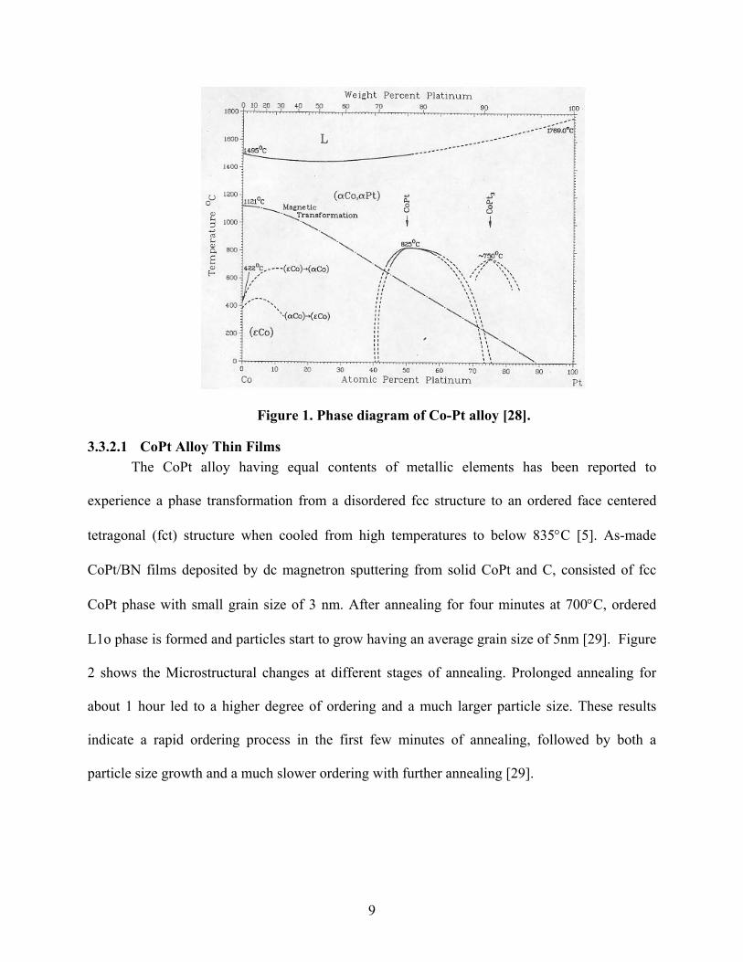
Figure 1. Phase diagram of Co-Pt alloy [28].
3.3.2.1 CoPt Alloy Thin Films The CoPt alloy having equal contents of metallic elements has been reported to
experience a phase transformation from a disordered fcc structure to an ordered face centered
tetragonal (fct) structure when cooled from high temperatures to below 835°C [5]. As-made
CoPt/BN films deposited by dc magnetron sputtering from solid CoPt and C, consisted of fcc
CoPt phase with small grain size of 3 nm. After annealing for four minutes at 700°C, ordered
L1o phase is formed and particles start to grow having an average grain size of 5nm [29]. Figure
2 shows the Microstructural changes at different stages of annealing. Prolonged annealing for
about 1 hour led to a higher degree of ordering and a much larger particle size. These results
indicate a rapid ordering process in the first few minutes of annealing, followed by both a
particle size growth and a much slower ordering with further annealing [29].

10
Figure 2. TEM images and SAD patterns of CoPt/BN at different annealing stages. (a) as-made; (b) optimum annealed sample; and (c) over annealed sample [29].
CoPt/C films have been deposited in another study by rf magnetron sputtering from solid
CoPt and C targets. The CoPt/C films deposited on Si consisted of Co-rich hexagonal Co-Pt
particles in a C matrix with a granular structure. After annealing for 10 minutes at 700°C, an fct
CoPt phase with larger particle size was formed. It is seen from Figure 3 that after prolonged
annealing to 60 minutes more ordered fct CoPt is formed with much larger particle size [30].
Figure 3. Micrographs and electron diffraction pattern of CoPt sample (a), (b) as-made; (c), (d) annealed at 700°C for 10 min; and (e),(f) annealed at 700°C for 60 min [30].

11
3.3.2.2 CoPt3 Alloy Thin Films From the phase diagram of Co-Pt system, at high temperatures a chemically disordered
fcc solid solution is known to exist over the whole composition range and at low temperatures
CoPt3 has a L12 fcc ordered phase. In the L12 phase, the majority atoms are located at the face
centers of fcc unit cell and the minority atoms at the corners, while in the disordered fcc phase
these sites are randomly occupied [31]. The bulk CoPt3 alloy has an order-disorder transition
temperature of 685°C with different Curie temperatures of ordered and disordered phases equal
to 15 and 195°C, respectively. CoPt3 (111) nanostructures prepared by self-assembling on WSe2
(0001) substrates, presented a (111) oriented fcc structure [31]. In another study, a continuous
CoPt3 (111) film epitaxially grown on Pt (111) or Ru (0001) showed a L12 long-range ordering
for deposition temperatures ranging between 550 and 700°C [4].
3.3.2.3 Co3Pt Alloy Thin Films From previous studies, it has been reported that, Co3Pt thin films undergo a
transformation from disordered fcc to disordered hcp structure [32]. Co3Pt films, deposited on Si
by RF sputtering had a mixture of fcc and hcp phases. The hcp phase had lattice constants of a =
2.6 Å and c = 4.22 Å. The fcc phase had a lattice constant a = 3.66 Å. Annealing these films
above 600°C altered the amount of one phase in the other. Annealing followed by rapid cooling,
resulted in fcc dominating over the hcp phase [32].
In recent times, it was reported that Co3Pt films grown by e-beam evaporation had an hcp
ordered structure and had lattice constants of a = 2.64 Å and c = 4.26 Å [15]. It has also been
reported that, ion implantation followed by thermal processing has been used to synthesize Co3Pt
films having disordered fcc structure with a lattice constant a = 3.67 Å [33].
In a study conducted recently, Co3Pt alloy thin films were deposited onto different
substrates like Borosilicate glass, fused silica, MgO (111) and Al2O3 (0001), by e-beam co-

12
evaporation using Co and Pt sources to analyze the effect of substrate on the crystal structure of
the film [11,12,13]. The substrates were held at temperatures between 25 and 500°C. The
structure of Co3Pt films deposited on Borosilicate glass was a mixture of fcc and hcp in which, a
(111) and (0001) texture in the film plane was developed. The structure of Co3Pt thin films
deposited on the MgO (111) and Al2O3 (0001) substrate was hcp [11,12]. Co3Pt film deposited
on Al2O3 showed a superlattice peak in the XRD spectrum in addition to the fundamental peaks
(shown in Figure 4), confirming partial ordering of the Co3Pt films [12,13]. The ordering is these
films have been reported to be produced by surface diffusion and the degree of ordering
depended on the rate of deposition and Ts [13].
Figure 4. XRD spectrum for a Co3Pt film on Al2O3 (0001) deposited at 400°C [12]. 3.4 Magnetism and Anisotropy Magnetism is a phenomenon by which a material asserts an attractive or repulsive force
on other materials [2]. Magnetic forces are generated by moving, electrically charged particles.
Each electron in an atom possesses a magnetic moment. Electron normally pair off in their
orbital with as many spins “up” and “down”. An atom will appear magnetic, only when there is
an unbalance in the spin of the electrons [34].

13
Magnetic materials contain domains. These are regions within the crystal in which all the
unit cells have a common magnetic orientation. All the unit cells within a phase have the same
arrangement of atoms. At higher temperatures, the magnetic dipoles of individual atoms are
oriented randomly. During cooling past the Curie temperature, a coupling develops between
magnetic dipoles of adjacent atoms. This coupling produces the same magnetic orientation
across many unit cells to develop a domain [34]. Adjacent domains are separated by domain
boundaries or walls, across which the direction of magnetization gradually changes. The
magnetic dipole orientation across a domain wall is shown in Figure 5. For a polycrystalline
material, there will be a large number of domains and all may have different magnetization
orientations [2].
Figure 5. A gradual change in the magnetic dipole orientation across a domain wall [2].
When a field H is applied to a material, then the domains change shape and size by the
movement of domain boundaries. Initially, the moments of the constituent domains are randomly
oriented such that there is no net M field. As the external field is applied, the domains that are
oriented in direction favorable to the applied field grow at the expense of the field strength until

14
the macroscopic specimen becomes a single domain, which is nearly aligned with the field.
Saturation is achieved when this domain, by means of rotation, becomes oriented with the H
field. From the saturation point, as the H field is reduced by the reversal of the field direction, the
curve does not retrace its original path.
A hysterisis effect is produced in which the B field lags behind the applied field H, or
decreases at a lower rate. At Zero H field, there exists a residual B field that is called remanence,
or remanent flux density Br; the material remains magnetized in the absence of an external H
field [1,2]. A typical hysterisis loop of a FM material is seen in Figure 6.
Figure 6. A typical hysterisis loop [2].
3.4.1 Anisotropy
One factor, which can strongly affect the shape of M, H (or B, H) curve or shape of the
hysterisis loop, is magnetic anisotropy. This term simply means that the magnetic properties
depend on the direction in which they are measured. There are several kinds of anisotropy and
some of them are crystal anisotropy, shape anisotropy, stress anisotropy, anisotropy induced by
magnetic annealing, plastic deformation and irradiation and exchange anisotropy [1].

15
3.4.1.1 Crystal Anisotropy Crystal anisotropy is the only type of anisotropy, which is intrinsic to the material while
all the rest of them are extrinsic or induced. Crystal anisotropy is due to spin orbit coupling.
Coupling means interaction. There is a coupling between the spin and orbital of each electron.
When an external field tries to reorient the spin of an electron, the orbit of that electron also
tends to reorient. As the orbit is strongly coupled with the lattice, it resists the attempt to rotate
the spin axis. The energy required to rotate the spin system of the domain away from the easy
direction is the energy required to overcome the spin orbit coupling and this is known as the
anisotropy energy. This coupling is relatively weak, as a few hundred Oersteds (Oe) is enough to
rotate the spin [1].
3.4.1.2 Shape Anisotropy A polycrystalline specimen having no preferred orientation of its grains therefore, has no
crystal anisotropy. If it is spherical in shape, the same applied field will magnetize it to the same
extent in any direction. But if it is nonspherical, it will be easier to be magnetized along a long
axis than along a short axis. The demagnetizing field along a short axis is stronger than along a
long axis. The applied field along a short axis then has to be stronger to produce the same true
field inside the specimen. Thus, shape alone can be a source of magnetic anisotropy [1]. This is
known as shape anisotropy.
3.4.1.3 Exchange Anisotropy Exchange bias or exchange anisotropy occurs when there is an exchange coupling of FM
and antiferromagnetic [AFM] films across their common interface causing a shift in the
hysterisis loop of the ferromagnet. This shift occurs after cooling the system with the magnetized
FM layer below the Neel temperature of the AFM [35]. This shift finds its application in
controlling the magnetization in devices, such as spin valves that sense the change in the

16
magnetic fields through the GMR effect. To measure the coercivity during this process,
obtaining the hysterisis loop is a convenient method. Here, the magnetization is saturated in one
direction and then the field is reversed linearly. As this is done, the hysterisis loop also shifts
leading to an increase in the width of the loop, which means an increase in the coercivity. The
characteristics of exchange bias depend on the constituent materials, thickness, temperature and
the orientation of the applied fields. Both coercivity and exchange bias depend on the
temperature. By increasing the temperature the exchange bias gets smaller while the coercivity
increases and reaches a peak. Finally, the exchange bias reaches zero and the coercivity
decreases again with increasing temperature and reaches a blocking temperature at which the
exchange bias disappears [36].
Exchange bias is more likely to be seen in FM/AFM bilayers when the Neel temperature
is greater than the Curie temperature. Exchange bias or exchange anisotropy was first discovered
when fine, single domain particles of Co were partially oxidized, such that each Co particle was
covered with a layer of CoO. This system was then cooled in a strong field to 77°K and its
hysterisis loop was measured at that temperature. The hysterisis loops were not symmetrical at
the origin and shifted to left along the magnetic field. This can be seen in Figure 7. The Co-CoO
particles showed a shift in the loop due to the exchange coupling between the spins of AFM CoO
and FM Co at the interface between them [1]. The Neel temperature of CoO is 20°C. When a
strong field is applied at 20°C the Co saturates and the oxide being paramagnetic is not really
affected. The Co ions in the oxide are forced to be aligned parallel to the adjoining spins of Co
metal, because of the positive exchange force between the spins of adjacent Co atoms. For the
establishment of exchange coupling there are three requirements. Firstly, field cooling is done
through the Neel temperature. Secondly, intimate contact between the AFM and FM is required,

17
such that the exchange coupling can occur across the interface. And lastly, there should be strong
crystal anisotropy in the AFM.
Figure 7. Hysterisis loops measured at 77°K of oxide-coated Co particles. Loop (1) results from cooling in a 10kOe field in the positive direction and loop; and (2) from cooling in zero field [1].
Exchange anisotropy has also been found in disordered Ni3Mn systems [1]. This system
is paramagnetic at room temperature and showed exchange anisotropy when cooled at low
temperatures. The loop is shifted so far that the retentivity is positive, after cooling in a field in
the positive direction. The reason for the exchange bias is due to the composition fluctuations in
the solid solution, which results in the formation of Mn rich clusters. The clusters are AFM;
because of the exchange force between the Mn-Mn nearest neighbors is negative spin pure Mn.
Outside the cluster the solid solution would be richer in Nickel than the average composition and
the preponderance of Ni-Ni and Ni-Mn nearest neighbors would cause ferromagnetism. It may
thus, be concluded that for the exchange anisotropy to occur the system need not be a two phase
alloy system, but can also be a single phase solid solution having the right kind of inhomogeneity
[1].

18
3.4.2 Magnetic Properties of Co-Pt Alloy and Multilayered Thin Films
There has been a drastic growth in the field of magnetic information storage systems in
the recent years. The most important parameters, which need to be taken into consideration in
recording media, are grain size and magnetic coupling across the grain boundaries [4].
The increase in areal density on the recording media has brought a revolutionary change
in the magnetic recording technology. The increase in the areal density implies the reduction in
size of the actual magnetic bits. One of the many issues concerning the high density recording
media is the media noise. Intergranular exchange coupling is one of the most important factors,
which contributes to limiting the media noise that helps in controlling the areal density [6].
Magnetically isolated grains of size less than 10 nm are preferred for high magnetic
recording density because of the need to reduce noise. In order to reduce thermal fluctuations and
demagnetizing fields in such small grain sizes of less than10 nm, they need to have high
magnetocrystalline anisotropy. It is believed that for high-density magnetic recording media
above 20 Gbits/in2, the thermal stability is one of the main concerns. The reason is that thermal
agitation is prominent for grain sizes less than 10 nm. To maintain good stability of written
marks, the magnetic anisotropy of grains should be greater than 107 ergs/cm3 and this is
attainable by Co-Pt thin films [11]. High magnetocrystalline anisotropy is needed to destabilize
the magnetization of the recorded bits. CoPt alloy thin films are of great interest due to their high
anisotropy and coercivity [5].
Most widely used recording method is the longitudinal recording. Here the
demagnetizing field gets stronger with the increase in the areal density and thus, influences the
stability of the magnetic domain. Perpendicular recording has the ability to decrease the effect of
demagnetizing field and can improve the stability of the magnetic domain. Large perpendicular

19
magnetic anisotropy (PMA) was seen in Co/Pt multilayers but the reason why they are not yet
used in real recording is that the existence of strong intergranular magnetic coupling, which is
the root, cause for transition media noise [3].
Co-Pt alloys are known for their high magnetic anisotropy and excellent coercivity [13].
The CoPt alloy thin films are used in magnetic devices like high density recording media and
magnetic bias films of magneto resistive elements. An assembly of very fine noninteracting high
anisotropy magnetic particles is magnetically hard which means it has large coercivity. This due
to the fact that particles are single domains and that magnetic reversal takes place only by
rotation of Ms vectors against strong anisotropy forces. The magnetic hardness of permanent
magnets depends on the size of the particles and the interaction between the particles. The
particle growth on a substrate depends on the strength of interaction between atoms of growing
film and the atoms of the substrate.
Magnetic properties of Co-Pt alloy thin films are a function of substrate, deposition
temperature and the composition of the film [11,12,21]. CoPt alloys containing rich Co
concentration are candidates for high magnetic anisotropy. CoPt films having equiatomic
compositions have excellent magneto-crystalline anisotropy. The Co3Pt alloy films show large
PMA [13]. This PMA depends on the composition and the type of substrate used.
The sensitivity of the magnetic moments of Pt atoms in the CoPt alloy system depends on
the concentration and local chemical environment. Therefore, the properties of the ordered
/disordered state at the Curie temperature are diagnosed. In the Co-Pt system, for a temperature
around 1400°K, the system orders ferromagnetically but stays atomically disordered in the
systems where the concentration of Co is larger than Pt. At 840°K, an ordered Co3Pt phase (L12)
with maximum ordering temperature was formed [37].

20
3.4.2.1 CoPt Alloy Thin films CoPt/Ag films consisting of fct CoPt have been subjected to annealing at different
temperatures to study the magnetic properties and microstructural changes. Figure 8 represents
the hysterisis loop of the film when annealed at different temperatures. This film was prepared
by magnetron sputter deposition, using co-sputtering from two metallic targets. The substrate
used was p-type Si (100) 60 µm thick [5]. It has been reported that CoPt alloy having equal
compositions of metallic elements experience a phase transformation from a disordered fcc
structure to an ordered fct structure when cooled from high temperature below 800°C [5]. When
annealed, these films transform into fct structure and become magnetically hard. It was also seen
that the coercivity increased drastically with the increase of temperature to 600°C. It was
reported that another important factor influencing coercivity is the layer thickness [5]. CoPt
films are known to have excellent magnetocrystalline anisotropy in the ordered face centered
tetragonal (fct) phase and can have coercivities greater than 5 kOe [30].
Figure 8. Hysterisis loops for CoPt/Ag films annealed for 2 hours at different temperatures [5].
21
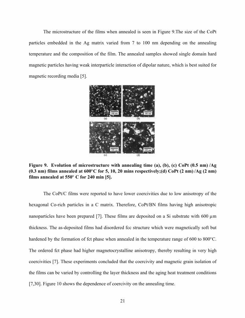
The microstructure of the films when annealed is seen in Figure 9.The size of the CoPt
particles embedded in the Ag matrix varied from 7 to 100 nm depending on the annealing
temperature and the composition of the film. The annealed samples showed single domain hard
magnetic particles having weak interparticle interaction of dipolar nature, which is best suited for
magnetic recording media [5].
Figure 9. Evolution of microstructure with annealing time (a), (b), (c) CoPt (0.5 nm) /Ag (0.3 nm) films annealed at 600°C for 5, 10, 20 mins respectively;(d) CoPt (2 nm) /Ag (2 nm) films annealed at 550° C for 240 min [5].
The CoPt/C films were reported to have lower coercivities due to low anisotropy of the
hexagonal Co-rich particles in a C matrix. Therefore, CoPt/BN films having high anisotropic
nanoparticles have been prepared [7]. These films are deposited on a Si substrate with 600 µm
thickness. The as-deposited films had disordered fcc structure which were magnetically soft but
hardened by the formation of fct phase when annealed in the temperature range of 600 to 800°C.
The ordered fct phase had higher magnetocrystalline anisotropy, thereby resulting in very high
coercivities [7]. These experiments concluded that the coercivity and magnetic grain isolation of
the films can be varied by controlling the layer thickness and the aging heat treatment conditions
[7,30]. Figure 10 shows the dependence of coercivity on the annealing time.
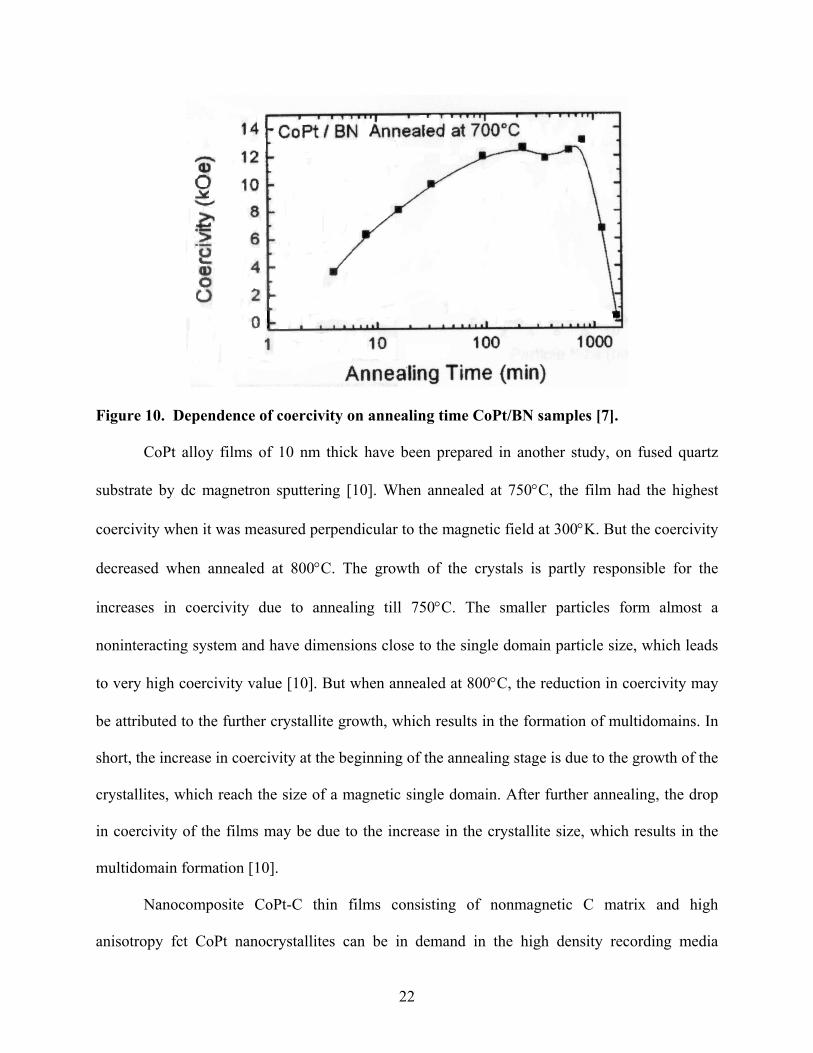
22
Figure 10. Dependence of coercivity on annealing time CoPt/BN samples [7].
CoPt alloy films of 10 nm thick have been prepared in another study, on fused quartz
substrate by dc magnetron sputtering [10]. When annealed at 750°C, the film had the highest
coercivity when it was measured perpendicular to the magnetic field at 300°K. But the coercivity
decreased when annealed at 800°C. The growth of the crystals is partly responsible for the
increases in coercivity due to annealing till 750°C. The smaller particles form almost a
noninteracting system and have dimensions close to the single domain particle size, which leads
to very high coercivity value [10]. But when annealed at 800°C, the reduction in coercivity may
be attributed to the further crystallite growth, which results in the formation of multidomains. In
short, the increase in coercivity at the beginning of the annealing stage is due to the growth of the
crystallites, which reach the size of a magnetic single domain. After further annealing, the drop
in coercivity of the films may be due to the increase in the crystallite size, which results in the
multidomain formation [10].
Nanocomposite CoPt-C thin films consisting of nonmagnetic C matrix and high
anisotropy fct CoPt nanocrystallites can be in demand in the high density recording media
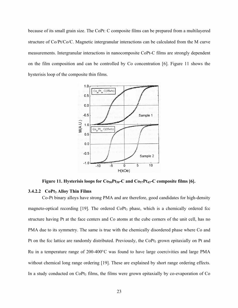
23
because of its small grain size. The CoPt: C composite films can be prepared from a multilayered
structure of Co/Pt/Co/C. Magnetic intergranular interactions can be calculated from the Μ curve
measurements. Intergranular interactions in nanocomposite CoPt-C films are strongly dependent
on the film composition and can be controlled by Co concentration [6]. Figure 11 shows the
hysterisis loop of the composite thin films.
Figure 11. Hysterisis loops for Co50Pt50-C and Co57Pt43-C composite films [6].
3.4.2.2 CoPt3 Alloy Thin Films Co-Pt binary alloys have strong PMA and are therefore, good candidates for high-density
magneto-optical recording [19]. The ordered CoPt3 phase, which is a chemically ordered fcc
structure having Pt at the face centers and Co atoms at the cube corners of the unit cell, has no
PMA due to its symmetry. The same is true with the chemically disordered phase where Co and
Pt on the fcc lattice are randomly distributed. Previously, the CoPt3 grown epitaxially on Pt and
Ru in a temperature range of 200-400°C was found to have large coercivities and large PMA
without chemical long range ordering [19]. These are explained by short range ordering effects.
In a study conducted on CoPt3 films, the films were grown epitaxially by co-evaporation of Co

24
and Pt from two e-beam sources on surface crystals of WSe2 (0001). A 3 nm thick CoPt3 film
had a coercivity of 200 Oe and a saturation magnetization of 520 emu/cm3. Increase in the
thickness of the film resulted in the decrease of domain size. A 6 nm thick CoPt3 films showed
strong PMA, and had very small grain size and hence can be used in data storage media [19].
3.4.2.3 Co3Pt Alloy Thin films For a long time no magnetic anisotropy was reported for Co3Pt alloy films. Yamada et al
[11,12,14] reported that large PMA exists in Co-Pt thin films rich in Co. Co3Pt alloy films, where
x is ranging from 0 to 0.5 with a thickness 1000+100 Å have been deposited by e-beam co-
evaporation on MgO, Al2O3, Borosilicate glass and fused silica substrates. The film has the
maximum PMA constant Ku at 25 at% Pt when compared to the other Co-Pt films of varying
compositions deposited on Borosilicate glass substrate [11]. Figure 12 shows the effect of Pt
concentration on the magnetic properties of the Co-Pt alloy system.
The Ku values of films deposited on MgO (111), Al2O3 (0001) and fused silica are
maximum in the substrate temperature range of 180 to 400°C. Therefore, it is said that the Co3Pt
film deposited on Al2O3, MgO and fused silica substrates using e-beam co-evaporation have a
PMA greater than 107 ergs/cm3 in the temperature range 180 to 400°C. The reasons for the high
PMA have been attributed to the anisotropic distribution of Co-Co bonds in the hcp ordered
structure [11].

25
Figure 12. Dependence of (a) coercivity; and (b) anisotropy constant on Pt content of the CoPt films deposited onto Borosilicate glass substrate at ambient temperatures [11].
A correlation between the origin of magnetic anisotropy and the ordered phase of Co3Pt
was made. The experiments suggested that the Ku is dependent on composition, nature of the
substrate and the substrate temperature [12,14]. Ku varies linearly with order parameter S for
substrate temperature Ts ranging from 380 to 450°C. No correlation was found in the temperature
range of 230 to 380°C. Hence, it has been concluded that S and Ku were dependent on Ts
[12,13,14].
3.4.2.4 Co/Pt Multilayered Films The multilayers of Co/Pt exhibit structure sensitive magnetic anisotropy and giant
magneto resistance (GMR). Co/Pt multilayer thin films have large ratio of coercive field to
saturation magnetization ratio. Pt/Co multilayers are found to exhibit large coercivities in both
sputtered and evaporated film [38]. The coercivities of sputtered Co/Pt films depend on the
26
annealing temperature in controlled atmospheres. Annealing has been performed in different
atmospheres like air and 10% H2 in N2 in the range of 100 to 400°C. The coercivity was found to
increase in atmospheres having large amount of O2. The coercivity also increased after annealing
in vacuum or in air. In the multilayer films, it was observed that as the coercivity increased, the
saturation magnetization decreased and hence it was concluded that an increase in coercivity is
due to the presence of CoO. It was also seen that annealing in 10%H2 in N2 reverses the increase
in coercivity. Initially, the reason for the increase of coercivity was thought to be the presence of
oxygen in the multilayered films but the further increase in coercivity was attributed to the
presence of domain wall pinning [38].
The multilayers of Co/Pt and Co/Cu are believed to exhibit structure sensitive magnetic
anisotropy and GMR [39]. Co, Pt layers have been deposited in the past on glass substrate using
ion-assisted deposition. The effects on the ion-treated Co/Pt multilayers can be compared to the
Co/Pt multilayers that are sputtered deposited in thermalizing conditions. These films had
rougher interfaces, coarser microstructures, stronger perpendicular anisotropy and larger
coercivities. There was a progressive loss of GMR and AFM coupling in the ion assisted Co/Cu
multilayers. This has been attributed to modifications of the microstructure and texture of the
layers or interface regions [39].
The above literature review shows that a lot of interest and investigative effort exists in
the area of Co-Pt alloy thin films and Co/Pt multilayers and their properties. An issue where very
little information exists is the synthesis of Co3Pt and Pt/Co multilayers with alternative technique
such as e-beam evaporation. Such an effort would help in better understanding the structural and
magnetic behavior of these thin films.
27
4 EXPERIMENTAL 4.1 Film Synthesis by EBPVD
Thin films of Co, Pt, Co-Pt alloy and Pt/Co multilayers were synthesized using the
EBPVD technique. All the films were deposited on the Si (100) substrate.
4.1.1 Processing System
An Edwards AUTO 306 Vacuum Coater with a cryo pump and a dual electron gun was
used to synthesize the thin films and multilayers. The system is designed for PVD under high
vacuum. This PVD system has two electron beam guns allowing flexibility for depositing
multilayered or alloy films. The EBPVD is a low temperature method, through which deposition
of alloy, composites and multilayers with sharp interfaces can be achieved.
The important components of the system are: two e-beam guns, a pumping system
consisting of a rotary mechanical pump and cryodrive pump, base plate, and an electrical system
with a controller. The system has a vacuum chamber attached to the base plate. Thickness
monitors are placed above the substrate holder to monitor the deposition rates. The work piece
holder and heater accessories are used to support and heat the substrate materials to be coated in
the vacuum chamber. The work piece holder ring can be adjusted horizontally or vertically
according to the experimental need. A radiant heater and a quartz heater are used to heat the
substrate before and during deposition process to prevent the adsorption of moisture and
contaminants by the substrate material. A quartz heater is used with the rotary work piece holder
and a radiant heater with the spherical work holder dome.
28
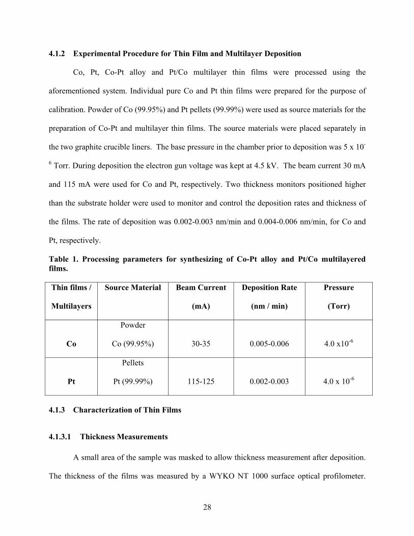
4.1.2 Experimental Procedure for Thin Film and Multilayer Deposition
Co, Pt, Co-Pt alloy and Pt/Co multilayer thin films were processed using the
aforementioned system. Individual pure Co and Pt thin films were prepared for the purpose of
calibration. Powder of Co (99.95%) and Pt pellets (99.99%) were used as source materials for the
preparation of Co-Pt and multilayer thin films. The source materials were placed separately in
the two graphite crucible liners. The base pressure in the chamber prior to deposition was 5 x 10-
6 Torr. During deposition the electron gun voltage was kept at 4.5 kV. The beam current 30 mA
and 115 mA were used for Co and Pt, respectively. Two thickness monitors positioned higher
than the substrate holder were used to monitor and control the deposition rates and thickness of
the films. The rate of deposition was 0.002-0.003 nm/min and 0.004-0.006 nm/min, for Co and
Pt, respectively.
Table 1. Processing parameters for synthesizing of Co-Pt alloy and Pt/Co multilayered films. Thin films /
Multilayers
Source Material Beam Current
(mA)
Deposition Rate
(nm / min)
Pressure
(Torr)
Co
Powder
Co (99.95%)
30-35
0.005-0.006
4.0 x10⁻⁶
Pt
Pellets
Pt (99.99%)
115-125
0.002-0.003
4.0 x 10⁻⁶
4.1.3 Characterization of Thin Films
4.1.3.1 Thickness Measurements
A small area of the sample was masked to allow thickness measurement after deposition.
The thickness of the films was measured by a WYKO NT 1000 surface optical profilometer.

29
This instrument functions on the principle of interference of light. The deposition rate of Co-Pt
thin films was estimated by the ratio of the observed thickness to the total deposition. Film
thickness was measured by using the surface optical profilometer at a magnification of 10X. The
phase shift interference (PSI) mode of the profilometer used for the measurement has a vertical
resolution of about 3 Å. Thickness values represent the average of at least three measurements.
4.1.3.2 Compositional and Microstructural Characterization
4.1.3.2.1 TEM High-resolution (HR) TEM analysis of Co-Pt as deposited films, Co-Pt annealed films
and Pt/Co multilayers was performed on a JEOL JEM 2010 electron microscope operated at 200
keV with a point-to-point resolution of 2.3 Å. Plan view and cross sectional TEM samples were
prepared for analysis. Cross sectional slices were obtained by cutting the samples along a
direction normal to the coating surface and then gluing, face-to-face the two coating surfaces.
Cross-sectional specimens for TEM observation were prepared by mechanical grinding,
polishing, and dimpling followed by Ar-ion milling using a Gatan Precision Ion Polishing
System (PIPSTM, Model 691) at 4.5 keV, at an angle of 5o.
4.1.3.2.2 SEM
A Hitachi S-3600N scanning electron microscope (SEM), equipped with an Energy
Dispersive Spectroscopy (EDS) detector, was used in this study to investigate the surface
morphology and composition of all films. Images in the SEM can be obtained using a secondary
electron detector or a back scattered electron detector. Some preliminary compositional analysis
of the Co-Pt and Pt/Co multilayer film was carried out with EDS. However, this technique has a
large excitation depth larger than the film thickness and thus may not be the most appropriate
technique for compositional analysis.

30
4.1.3.2.3 Microprobe
A JAX-733 electron microprobe was used for compositional analysis of thin films.
Microprobe is using an electro beam accelerated at a voltage of 15 kV and a beam current of 10
nA. The microprobe has a wavelength dispersive spectrometer (WDS) allowing accurate
compositional analysis based on the characteristic wavelength of X-rays emitted by each
element.
4.1.3.3 Characterization of Magnetic Properties of Thin Films
4.1.3.3.1 MPMS
The Quantum Design’s Magnetic Property Measurement system (MPMS) is a highly
integrated instrument, designed to be a primary research tool for magnetic properties. A MPMS–
5 model was used for analysis. It has a field range of –5.5 to +5.5 Tesla i.e., 55000 Gauss and a
field stability of 1 ppm. The temperature range at the sample space is 1.9°K to 400°K and it has a
He capacity of 56 l. The principle components of this measurement comprise of a temperature
control system, magnet control system, superconducting SQUID amplifier system, sample
handling system and a computer operating system.
In the magnet control system, the current from a power supply is set to provide magnetic
fields from zero to positive and negative seven teslas. The magnet can be operated in either
persistent or non-persistent modes, and the user can select several charging options. In the
superconducting SQUID amplifier system, the rf SQUID detector is the heat of the magnetic
31
moment detection system. It provides reset circuitry, auto ranging capability, a highly balanced
second derivative sample coil array and EMI protection.
The ability to step and rotate the sample smoothly through the detection coils without
transmitting undue mechanical vibration to the SQUID is of primary importance. The sample
handling system allows for varied scan lengths and options as to how data are acquired for a
given measurement. All operating features of the MPMS are under automated, computer control.
The user interface at the PC console provides the option of working under standard sequence
controls, or diagnostic controls, which will invoke individual functions. For the MPMS,
superconductivity is the critical enabling technology that provides for both the production of
large, very stable magnetic field, and the ability to measure changes in those fields, which are 14
orders of magnitude smaller.
4.1.3.3.2 PPMS
The Quantum Design’s Physical Property Measurement System (PPMS) is a versatile DC
magnetometer and AC susceptometer. A MODEL 6000 was used for analysis in the present
study. It has a field range of –9.0 to +9.0 Tesla i.e., 90000 Gauss. The AC Measurement System
(ACMS) insert houses the drive and detection coils, thermometer and electrical connections for
the ACMS system. The insert fits directly into the PPMS sample chamber and contains a sample
space that lies within a uniform magnetic field region of host PPMS, so the DC field and the
temperature control can be performed with conventional PPMS methods. The sample is held
within the insert coil set on the end of a thin rigid sample rod. A DC servomotor located in the
ACMS sample transport assembly translates the sample holder longitudinally. The DC
servomotor provides rapid and very smooth longitudinal sample motion. The ACMS sample
transport assembly mounts on the top of the PPMS probe.
32
During DC measurements, a constant field is applied to the measurement region and the
sample is moved quickly through both sets of coils inducing a signal in them according to the
Faradays law. During DC measurement, the amplitude of the detection coil signal is dependent
upon both the extraction speed and the samples magnetic moment.

33
5 RESULTS AND DISCUSSION
Thin films of pure Co, pure Pt, as-deposited Co-Pt alloy, annealed Co-Pt alloy and Pt/Co
multilayers were characterized by profilometry, SEM, TEM, MPMS and PPMS. The Co-Pt alloy
film composition was obtained using the electron microprobe analysis, and was found to have Co
and Pt in the atomic ratio of 3:1. Thickness of the films was measured using profilometry.
Surface morphology was characterized using SEM and microstructure was studied using TEM.
MPMS and PPMS were used for measuring magnetic properties of the films. Results obtained
from the above experiments are presented in the following sections.
5.1 Microstructure of Synthesized Films 5.1.1 As-deposited Films
5.1.1.1 Pure Co Film
Figure 13 shows a typical TEM micrograph of a 21 nm thick pure Co film deposited on
TEM Cu grit. Inset is a selected-area electron diffraction pattern (SAED) from the film.
Microstructure of the film shows a nodular structure with an average grain size in the range of 6
to 7 nm. The Co film may have nanocrystalline grains of CoO along with Co grains. From the
electron diffraction pattern, the Co seems to have a mixture of hcp and ε structure, whereas the
CoO has a structure similar to NaCl. The diffraction rings of the SAED pattern in Figure 13 have
a d-spacing of 2.51, 2.22, 1.99, 1.52, 1.29, 1.2, 1.09, 0.98, 0.89, 0.83, 0.71 and 0.63 Å.
i. The d-spacing of 2.51, 1.52, 1.29, 1.2, 1.09, 0.98, 0.89, 0.83, 0.71 and 0.63 Å
corresponds to the (111), (220), (311), (222), (400), (331), (422), (333), (600) and (622)
reflection of NaCl type CoO.
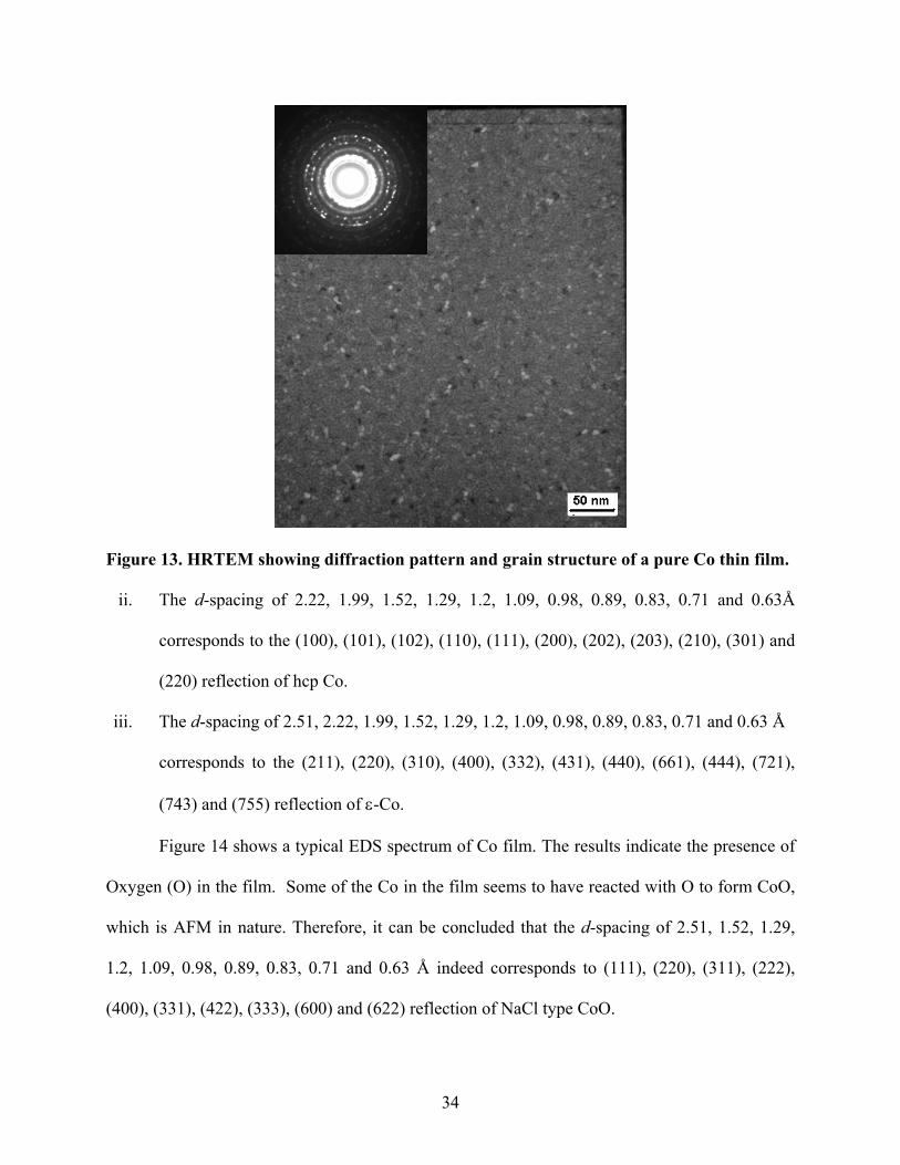
34
Figure 13. HRTEM showing diffraction pattern and grain structure of a pure Co thin film.
ii. The d-spacing of 2.22, 1.99, 1.52, 1.29, 1.2, 1.09, 0.98, 0.89, 0.83, 0.71 and 0.63Å
corresponds to the (100), (101), (102), (110), (111), (200), (202), (203), (210), (301) and
(220) reflection of hcp Co.
iii. The d-spacing of 2.51, 2.22, 1.99, 1.52, 1.29, 1.2, 1.09, 0.98, 0.89, 0.83, 0.71 and 0.63 Å
corresponds to the (211), (220), (310), (400), (332), (431), (440), (661), (444), (721),
(743) and (755) reflection of ε-Co.
Figure 14 shows a typical EDS spectrum of Co film. The results indicate the presence of
Oxygen (O) in the film. Some of the Co in the film seems to have reacted with O to form CoO,
which is AFM in nature. Therefore, it can be concluded that the d-spacing of 2.51, 1.52, 1.29,
1.2, 1.09, 0.98, 0.89, 0.83, 0.71 and 0.63 Å indeed corresponds to (111), (220), (311), (222),
(400), (331), (422), (333), (600) and (622) reflection of NaCl type CoO.

35
Figure 14. EDS spectrum of a pure Co film.
5.1.1.2 Pure Pt Film Figure 15 shows a typical TEM micrograph of a Pt film deposited on TEM Cu grit. The
microstructure of the film shows a nodular structure with an average grain size in the range of 3
to 4 nm. The diffraction rings in the SAED pattern in Figure 15 have a d-spacing of 2.63, 2.22,
1.38, 1.16, 0.99, 0.88, 0.80, 0.76 and 0.66 Å.
i. The d-spacing 2.63, 2.22, 1.38, 1.16, 0.99, 0.88, 0.80, 0.76 and 0.66 Å corresponds to
(111), (200), (220), (311), (400), (420), (422), (333) and (531) reflection of fcc Pt.
Therefore, it can be concluded that the pure Pt film has an fcc structure.

36
Figure 15. HRTEM showing diffraction pattern and grain structure of a pure Pt thin film.
5.1.1.3 Co-Pt Film Figure 16 shows a plan view TEM micrograph of a typical Co-Pt thin film with an
original thickness of 145 nm. The microstructure shows an average grain size in the range of 5 to
6 nm. A mixture of fcc and hcp Co3Pt seem to exist along with the presence of ε-Co and NaCl
type CoO. The lattice constants of hcp Co3Pt are a =2.64 Å and c = 4.21 Å. The lattice constant
of fcc Co3Pt a = 3.69 Å. The lattice constant of simple cubic ε-Co, a = 6.12 Å. The diffraction
rings in Figure 16 show a d-spacing of 2.51, 2.22, 1.87, 1.52, 1.31, 1.11, 0.93, 0.84, 0.76, 0.72
and 0.63 Å.
i. The d-spacing 2.51, 1.52, 1.31, 1.11, 0.93, 0.84, 0.76, 0.72 and 0.63 Å corresponds to
(111), (220), (311), (400), (420), (333), (440), (531) and (622) reflection of NaCl type
CoO.
ii. The d-spacing 2.22, 1.52, 1.31, 1.11, 0.93, 0.84, 0.76, 0.72 and 0.63 Å corresponds to
(100), (101), (110), (201), (202), (211), (300), (302) and (222) reflection of hcp Co3Pt.

37
iii. The d-spacing 1.87,1.31, 1.11, 0.93, 0.84, 0.76, 0.72 and 0.63 Å corresponds to (200),
(220), (311), (400), (331), (422), (511) and (531) reflection of fcc Co3Pt.
Figure 16. HRTEM showing the grain structure of as-deposited Co-Pt alloy thin film. iv. The d-spacing 2.51, 2.22, 1.87, 1.52, 1.31, 1.11, 0.93, 0.84, 0.76, 0.72 and 0.63 Å
corresponds to the (211), (220), (311), (400), (332), (521), (533), (720), (740), (743) and
(763) reflection of ε-Co.
Figure 17 shows a typical EDS spectrum of an as-deposited Co-Pt alloy thin film. Again,
the presence of O is observed, which supports the conclusion that CoO is present in this film and
that the d-spacing of 2.51, 1.52, 1.31, 1.11, 0.93, 0.84, 0.76, 0.72 and 0.63 Å indeed corresponds
to (111), (220), (311), (400), (420), (333), (440), (531) and (622) reflection of NaCl type CoO.

38
Figure 17. EDS spectrum of as-deposited Co-Pt alloy thin film. 5.1.2 Annealed Films
5.1.2.1 Annealing at 300°C
Figure 18 shows a plan view TEM micrograph of a vacuum-sealed Co-Pt film, annealed
at 300°C in a high temperature furnace for 2 hours. The microstructure of the film shows an
average grain size of about 6 to 7 nm. Grains of the annealed film show a slight growth when
compared to the grains of the as-deposited Co-Pt film. The diffraction rings in Figure 18 have a
d-spacing of 2.51, 2.22, 1.81, 1.47, 1.31, 1.11, 1.05, 0.95, 0.83, 0.75, 0.71 and 0.64 Å.
i. The d-spacing 2.51, 1.47, 1.31, 1.05, 0.95, 0.83, 0.75, 0.71 and 0.64 Å corresponds to
(111), (220), (311), (400) (420), (333), (440), (600) and (622) reflection of NaCl type
CoO.
ii. The d-spacing 2.22, 1.31, 1.11, 1.05, 0.95, 0.83, 0.75, 0.71 and 0.64 Å corresponds to
(100), (110), (112), (202), (113), (211), (301), (302) and (310) reflection of hcp Co3Pt.

39
Figure 18. HRTEM showing diffraction pattern and grain structure of a Co-Pt alloy thin film annealed at 300°C. iii. The d-spacing of 1.81, 1.31, 1.11, 1.05, 0.95, 0.83, 0.75, 0.71 and 0.64 Å corresponds to
(200), (220), (311), (222), (400), (420), (422), (511) and (440) reflection of fcc Co3Pt.
iv. The d-spacing of 2.51, 2.22, 1.81, 1.47, 1.31, 1.11, 1.05, 0.95, 0.83, 0.75, 0.71 and 0.64 Å
corresponds to (211), (220), (311), (410), (332), (521), (433), (621), (721), (741), (743)
and (754) reflection of ε-Co.
Again, a mixture of fcc and hcp Co3Pt seems to exist along with of ε-Co and NaCl type
CoO as seen in the case of the as-deposited film.
Figures 19 and 20 show the SE and BSE image of a Co-Pt alloy film annealed at 300°C.
SE image usually shows the topography of the phases in a film. Regions appearing dark in the
image are higher in topography than the regions appearing bright. The different phases in a film
can be analyzed using BSE. The constituent phase appearing bright in a BSE image is denser
(high atomic number, Z) than the phase appearing dark. Since Co3Pt has a higher density and is
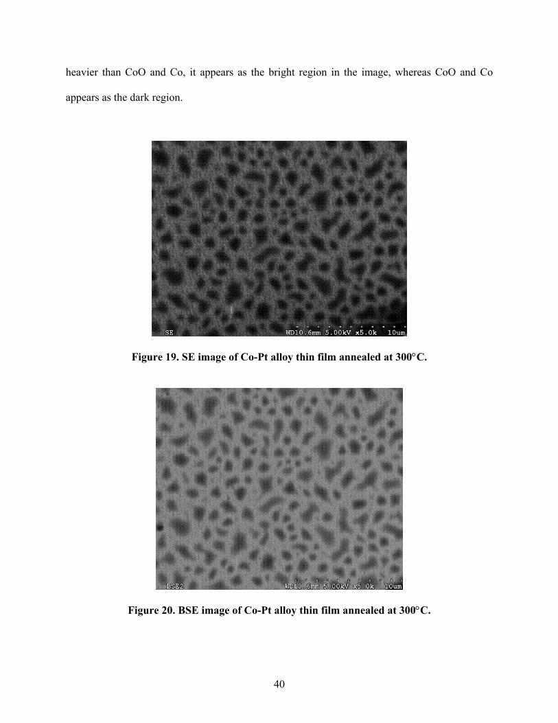
40
heavier than CoO and Co, it appears as the bright region in the image, whereas CoO and Co
appears as the dark region.
Figure 19. SE image of Co-Pt alloy thin film annealed at 300°C.
Figure 20. BSE image of Co-Pt alloy thin film annealed at 300°C.

41
Figure 21. EDS spectrum of a Co-Pt alloy thin film annealed at 300°C.
Figure 21 shows a typical EDS spectrum of a Co-Pt alloy film annealed at 300°C. The
presence of O, Co and Pt is observed along with Si. It is more likely that O is present in the form
of CoO, as the formation of Pt oxide is very difficult to occur.
5.1.2.2 Annealing at 400°C Figure 22 shows the plan view TEM micrograph of a Co-Pt film, which is vacuum-sealed
in glass and annealed at 400°C in a high temperature furnace for 2 hours. Microstructure of the
film indicates an average grain size of 10 nm. A significant grain growth is observed when the
specimen is annealed at 400°C. The diffraction rings in Figure 23 have a d-spacing of 4.53, 2.86,
2.41, 2.12, 2.03, 1.84, 1.64, 1.54, 1.47, 1.42, 1.35, 1.26, 1.22, 1.13 and 1.04 Å.
i. The d-spacing of 2.41, 2.12, 1.54, 1.26, 1.22 and 1.04 Å corresponds to (111), (200),
(220), (311), (222) and (400) reflection of NaCl type CoO.

42
Figure 22. HRTEM showing the grain structure of a Co-Pt alloy thin film annealed at 400°C.
ii. The d-spacing of 2.03, 1.54, 1.35, 1.26, 1.22, 1.13 and 1.04 Å corresponds to (101),
(102), (110), (111), (103), (112) and (202) reflection of hcp Co3Pt.
iii. The d-spacing of 2.12, 1.84, 1.35, 1.13 and 1.04 Å corresponds to (111), (200), (220),
(311), (222) and (400) reflection of fcc Co3Pt.
iv. The d-spacing of 4.53, 2.86, 2.41, 2.12, 2.03, 1.84, 1.64, 1.54, 1.47, 1.42, 1.35, 1.26,
1.22, 1.13 and 1.04 Å corresponds to (110), (210), (211), (220), (300), (311), (321),
(400), (410), (330), (421), (422), (430), (432) and (531) reflection of ε-Co.
The surface morphology of the Co-Pt thin film annealed at 400°C is shown in Figure 23.
A significant change in morphology of the film is seen when compared to film annealed at
300°C. This indicates that heat treatments at different temperatures have a significant effect on
surface morphology of the films. A rather uniform distribution of the particles is shown in
Figure 23, suggesting some rearrangement under the high temperature exposure.

43
Figure 23. SE image of a Co-Pt alloy thin film annealed at 400 °C.
Figure 24. EDS spectrum of a Co-Pt alloy thin film annealed at 400°C.
Figure 24 presents the EDS spectrum of a film annealed at 400°C. The EDS spectra of all
the films showed presence of O. Though, the exact source of O is not clearly known, Co has a
tendency of easily reacting with O to form CoO. Therefore, either Co may have reacted with O
44
immediately after the film deposition, or oxidation may have occurred in the film during vacuum
sealing of the sample.
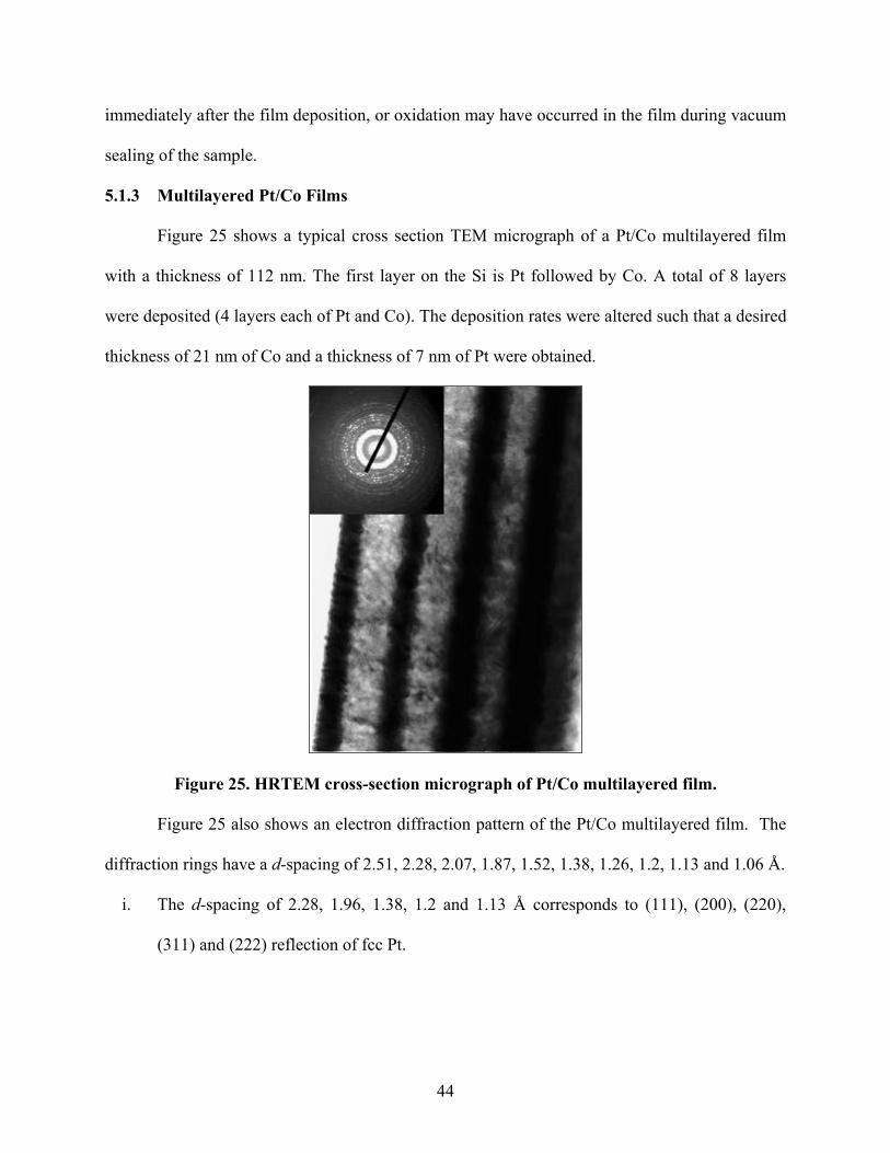
5.1.3 Multilayered Pt/Co Films
Figure 25 shows a typical cross section TEM micrograph of a Pt/Co multilayered film
with a thickness of 112 nm. The first layer on the Si is Pt followed by Co. A total of 8 layers
were deposited (4 layers each of Pt and Co). The deposition rates were altered such that a desired
thickness of 21 nm of Co and a thickness of 7 nm of Pt were obtained.
Figure 25. HRTEM cross-section micrograph of Pt/Co multilayered film.
Figure 25 also shows an electron diffraction pattern of the Pt/Co multilayered film. The
diffraction rings have a d-spacing of 2.51, 2.28, 2.07, 1.87, 1.52, 1.38, 1.26, 1.2, 1.13 and 1.06 Å.
i. The d-spacing of 2.28, 1.96, 1.38, 1.2 and 1.13 Å corresponds to (111), (200), (220),
(311) and (222) reflection of fcc Pt.

45
Figure 26. EDS spectrum of a Pt /Co multilayered film of thickness 112 nm.
ii. The d-spacing of 2.51, 2.07, 1.87, 1.52, 1.38, 1.26, 1.2, 1.13 and 1.06 Å corresponds to
(211), (221), (300), (400), (420), (422), (431), (432) and (441) reflection of ε-Co.
iii. The d-spacing of 1.87, 1.52, 1.26, 1.2, 1.13 and 1.06 Å corresponds to (101), (102),
(110), (111), (103) and (112) reflection of hcp Co.
iv. The d-spacing 2.51, 1.52, 1.26, 1.2 and 1.06 Å corresponds to (111), (220), (311), (222)
and (400) reflection of NaCl type CoO.
Figure 26 presents a typical EDS spectrum of a Pt/Co multilayered film and shows the
presence of Co and Pt. There may be some O, present in the film. However, there is no
corresponding peak visible. The presence of O can be explained by the d-spacing of 2.51, 1.52,
1.26, 1.2 and 1.06 Å corresponding to (111), (220), (311), (222) and (400) reflection of NaCl
type CoO.
46
5.2 Magnetic Property Measurements
Magnetic properties can be mainly performed in two different ways using the in-plane
(field parallel to the film) and perpendicular (field normal to the film) measurement methods.
The pure Co film, as-deposited Co-Pt alloy film, and Co-Pt alloy films annealed at 300°C and
400°C were measured for hysterisis using the MPMS at 10°K and 300°K. The magnetic
measurements were conducted at two different orientations namely, parallel and perpendicular.
5.2.1 In-Plane Measurements
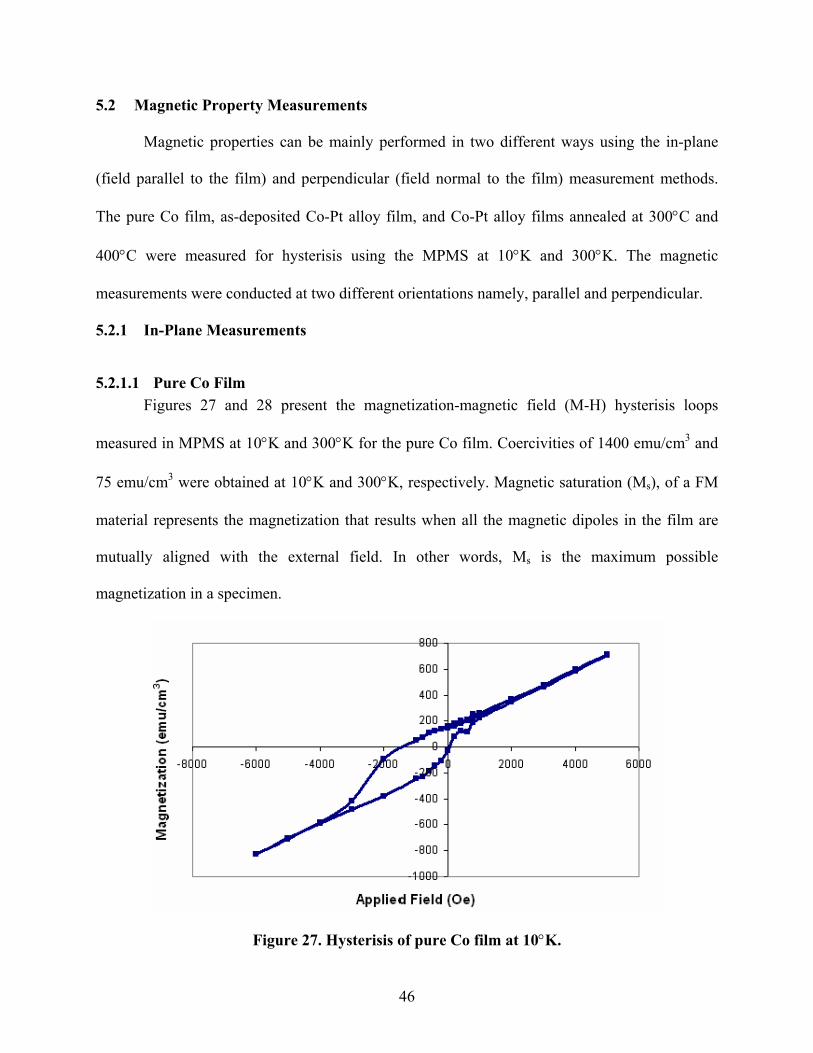
5.2.1.1 Pure Co Film Figures 27 and 28 present the magnetization-magnetic field (M-H) hysterisis loops
measured in MPMS at 10°K and 300°K for the pure Co film. Coercivities of 1400 emu/cm3 and
75 emu/cm3 were obtained at 10°K and 300°K, respectively. Magnetic saturation (Ms), of a FM
material represents the magnetization that results when all the magnetic dipoles in the film are
mutually aligned with the external field. In other words, Ms is the maximum possible
magnetization in a specimen.
Figure 27. Hysterisis of pure Co film at 10°K.

47
Figure 28. Hysterisis of a pure Co film at 300°K.
Ms of 300 emu/cm3 is obtained at 300°K. At 10°K the film does not saturate, even after
applying a field of 50 kOe. From this, it can be concluded that, pure Co film saturates easily at
room temperature and has a higher saturation value at lower temperatures.
5.2.1.2 Co-Pt As-deposited Film Figures 29 and 30 present hysterisis loops measured at 10°K and 300°K, respectively for
the as-deposited Co-Pt alloy thin film. Coercivities of 2490 emu/cm3 and 98 emu/cm3 were
obtained at 10°K and 300°K, respectively. Ms for the as-deposited Co-Pt alloy at 300°K is
around 370 emu/cm3. But, Ms at 10°K does not occur, even after applying a field of 50 kOe. The
Ms of pure Co is lower than that of as-deposited Co-Pt alloy film. Therefore, it can be concluded
that, addition of Pt to Co, has increased the Ms of Co.

48
Figure 29. Hysterisis loop of a Co-Pt as-deposited film at 10°K.
Figure 30. Hysterisis loop of a Co-Pt as-deposited film at 300°K.
5.2.1.3 Co-Pt Alloy Thin Film Annealed at 300°C Figures 31 and 32 show the hysterisis loops for a Co-Pt alloy film annealed at 300°C,
measured at 10°K and 300°K, respectively. Coercivities of 1960 emu/cm3 and 91 emu/cm3 were
obtained at 10°K and 300°K, respectively. Ms values could not be obtained at 10°K and 300°K,

49
as the film does not saturate, even after applying a field of 50 kOe. It is clearly seen that,
annealing the film at 300°C, has increased the saturation of Co-Pt alloy film to a large extent.
Figure 31. Hysterisis loop at 10°K for Co-Pt film annealed at 300°C.
Figure 32. Hysterisis loop at 300°K for Co-Pt film annealed at 300°C.
5.2.1.4 Co-Pt Alloy Thin Film Annealed at 400°C Figures 33 and 34 present hysterisis loops of Co-Pt alloy film annealed at 400°C, which
was measured at 10°K and 300°K, respectively. Coercivities of 1280 emu/cm3 and 100 emu/cm3
were obtained at 10°K and 300°K, respectively. Ms values were not obtained at 10°K and 300°K,

50
as the film did not saturate, even after applying a field of 50 kOe. A similar trend in the hysterisis
loop is seen in Co-Pt film annealed at 300°C. So it may be concluded, that annealing has an
effect on the magnetic properties of the film.
Figure 33. Hysterisis loop at 10°K for Co-Pt film annealed at 400°C.
Figure 34. Hysterisis loop at 300°K for Co-Pt film annealed at 400°C.
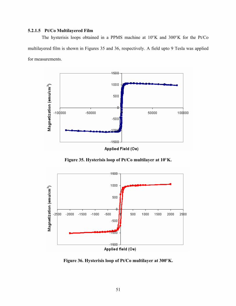
51
5.2.1.5 Pt/Co Multilayered Film The hysterisis loops obtained in a PPMS machine at 10°K and 300°K for the Pt/Co
multilayered film is shown in Figures 35 and 36, respectively. A field upto 9 Tesla was applied
for measurements.
Figure 35. Hysterisis loop of Pt/Co multilayer at 10°K.
Figure 36. Hysterisis loop of Pt/Co multilayer at 300°K.
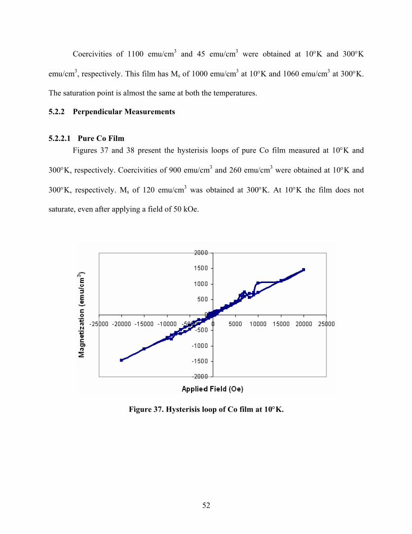
52
Coercivities of 1100 emu/cm3 and 45 emu/cm3 were obtained at 10°K and 300°K
emu/cm3, respectively. This film has Ms of 1000 emu/cm3 at 10°K and 1060 emu/cm3 at 300°K.
The saturation point is almost the same at both the temperatures.
5.2.2 Perpendicular Measurements
5.2.2.1 Pure Co Film Figures 37 and 38 present the hysterisis loops of pure Co film measured at 10°K and
300°K, respectively. Coercivities of 900 emu/cm3 and 260 emu/cm3 were obtained at 10°K and
300°K, respectively. Ms of 120 emu/cm3 was obtained at 300°K. At 10°K the film does not
saturate, even after applying a field of 50 kOe.
Figure 37. Hysterisis loop of Co film at 10°K.

53
Figure 38. Hysterisis loop of Co thin film at 300°K.
5.2.2.2 Co-Pt As-deposited Film Figures 39 and 40 present the hysterisis loops of an as-deposited Co-Pt alloy film
measured at 10°K and 300°K, respectively. Coercivities of 2200 emu/cm3 and 262 emu/cm3 were
obtained at 10°K and 300°K, respectively.
Figure 39. Hysterisis loop of as-deposited Co-Pt film at 10°K.
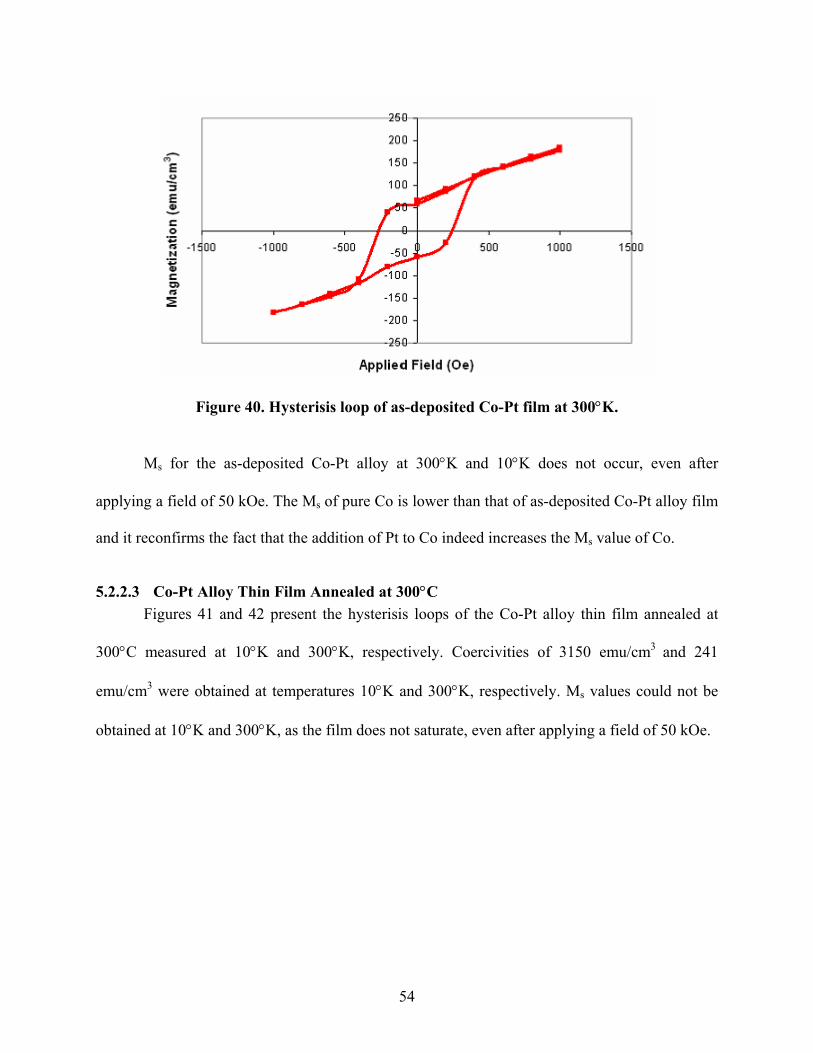
54
Figure 40. Hysterisis loop of as-deposited Co-Pt film at 300°K.
Ms for the as-deposited Co-Pt alloy at 300°K and 10°K does not occur, even after
applying a field of 50 kOe. The Ms of pure Co is lower than that of as-deposited Co-Pt alloy film
and it reconfirms the fact that the addition of Pt to Co indeed increases the Ms value of Co.
5.2.2.3 Co-Pt Alloy Thin Film Annealed at 300°C Figures 41 and 42 present the hysterisis loops of the Co-Pt alloy thin film annealed at
300°C measured at 10°K and 300°K, respectively. Coercivities of 3150 emu/cm3 and 241
emu/cm3 were obtained at temperatures 10°K and 300°K, respectively. Ms values could not be
obtained at 10°K and 300°K, as the film does not saturate, even after applying a field of 50 kOe.
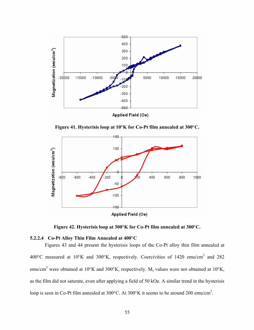
55
Figure 41. Hysterisis loop at 10°K for Co-Pt film annealed at 300°C.
Figure 42. Hysterisis loop at 300°K for Co-Pt film annealed at 300°C.
5.2.2.4 Co-Pt Alloy Thin Film Annealed at 400°C Figures 43 and 44 present the hysterisis loops of the Co-Pt alloy thin film annealed at
400°C measured at 10°K and 300°K, respectively. Coercivities of 1420 emu/cm3 and 282
emu/cm3 were obtained at 10°K and 300°K, respectively. Ms values were not obtained at 10°K,
as the film did not saturate, even after applying a field of 50 kOe. A similar trend in the hysterisis
loop is seen in Co-Pt film annealed at 300°C. At 300°K it seems to be around 200 emu/cm3.
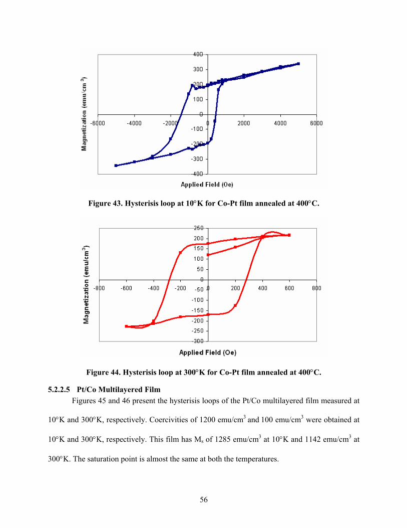
56
Figure 43. Hysterisis loop at 10°K for Co-Pt film annealed at 400°C.
Figure 44. Hysterisis loop at 300°K for Co-Pt film annealed at 400°C.
5.2.2.5 Pt/Co Multilayered Film Figures 45 and 46 present the hysterisis loops of the Pt/Co multilayered film measured at
10°K and 300°K, respectively. Coercivities of 1200 emu/cm3 and 100 emu/cm3 were obtained at
10°K and 300°K, respectively. This film has Ms of 1285 emu/cm3 at 10°K and 1142 emu/cm3 at
300°K. The saturation point is almost the same at both the temperatures.

57
Figure 45. Hysterisis loop of Pt/Co multilayer at 10°K.
Figure 46. Hysterisis loop of Pt/Co multilayer at 300°K.
Tables 2 and 3 present he coercivities of pure Co, as-deposited, annealed Co-Pt alloy and
Pt/Co multilayered thin films measured in both parallel and perpendicular directions to the
applied fields.
58
Table 2. Coercivity comparison of various films at different temperatures, in parallel measurements.
Table 3. Coercivity comparisons of various films at different temperatures, in perpendicular measurements.
Coercivity (emu/cm3) Temperature
Sample Name
10°K 300°K
Pure Co Film 900 260
As-deposited 2200 262
300 Annealed 3150 241 Co-Pt Thin Film
400 Annealed 1420 282
Pt/Co Multilayered Film 1200 100
For AFM materials, the Neel temperature is used for analyzing the magnetic properties,
whereas for FM materials, the Curie temperature is used for analyzing the magnetic properties.
Above the Neel temperature, an AFM material changes into a paramagnetic material, whereas
above the Curie temperature, an FM material turns into a paramagnetic material. Tables 4 and 5
show the Curie and Neel temperatures of some magnetic materials.
Coercivity (emu/cm3)
Temperature
Sample Name 10°K 300°K
Pure Co Film 1400 75
As- deposited 2490 98
300 Annealed 1960 91 Co-Pt Thin Film
400 Annealed 1280 100
Pt/Co Multilayered Film 1100 45
59
Table 4. Curie temperatures of FM materials.
Sample Curie Temperature (°K)
Co 1382-1400
CoPt 830
Table 5. Neel temperatures of AFM materials.
Sample Neel Temperature (°K)
CoO 260-280
Co3O4 40
A shift is observed in the hysterisis loops of all films, along the magnetic field axis at
10°K. This may be due to the exchange anisotropy or exchange bias phenomenon. Exchange bias
occurs due to the exchange coupling of FM / AFM layers, leading to a shift in the hysterisis loop
along the magnetic field axis. This shift usually occurs after field cooling the system containing
the magnetized FM layer below the Neel temperature of AFM layer. During cooling these AFM
domains lead to a small net magnetization at the FM /AFM interface. This magnetization is
stabilized towards lower temperatures resulting in a shift in the hysterisis loop. All the hysterisis
measurements in the present experiments have been conducted under zero-field cooling, where
cooling takes place without the presence of any external fields. The shift in hysterisis loop is not
possible at zero-field cooling. Hence, there is a possibility of the existence of some residual field
in the MPMS, during the magnetic measurements, which results in a shift in the hysterisis loops
at 10°K.
EDS spectra indicates the presence of O along with Co and Pt in the films. Co and Co3Pt
are FM whereas CoO is AFM in nature. The Neel temperature of CoO exists somewhere
between 260 and 280°K. At 10°K, which is below the Neel temperature of AFM CoO, exchange

60
interactions may have taken place at the FM/AFM interface resulting in the exchange anisotropy.
This may be a reason for the shift in hysterisis loops at 10°K, subsequently leading to an increase
in coercivity of the films. At 300°K, symmetric hysterisis loops are observed at which indicate
no exchange bias has occurred.
Temperature is one of the most important factors taken into consideration while
measuring magnetic properties. It is well known that raising the temperature causes an increase
in the magnitude of thermal vibrations of atoms in the material. Since the magnetic moments are
free to rotate, an increase in the temperature causes an increase in the thermal vibrations of the
atoms and tends to randomize the direction of any moments that may be aligned. In a FM and
AFM material, atomic thermal motions counteract the coupling forces between adjacent atomic
dipole moments, causing some dipole misalignment, regardless of whether an external field is
present or not. This results in a decrease in the Ms in the FM materials. At 0°K the maximum
value for Ms is obtained, since thermal vibrations are minimum at this temperature. As the
temperature increases, Ms decreases and becomes zero at the Curie temperature [1]. In this study,
the magnetic measurements were conducted at 10°K and 300°K. As a general trend it has been
observed that the Ms is maximum for measurements conducted at 10°K.
Tables 3 and 4 present the coercivities of various films measured in two different
orientations namely, parallel and perpendicular. In parallel measurement, the field is applied
along the easy axis of the film and the hysterisis loop is expected to be a square in shape. The Ms
and coercivity can be measured directly from the loop. In perpendicular measurement, the field is
applied along a hard axis that produces the linear M, H relation [2]. A typical hysterisis loop of
this kind is shown in Figures 37 and 39. If the field is large enough to produce saturation, the
film breaks up into domains upon reduction of the field. The easy axis coercivity is usually less

61
than hard axis coercivity. This can be seen in as-deposited and annealed of Co-Pt and Pt/Co
multilayered films.
Coercivities of the Co-Pt as-deposited and Co-Pt annealed films are much lower when
compared to corresponding values of Co3Pt films reported earlier. One of the reasons for this
behavior may be the presence of O in the films. From the SAED patterns, it can be concluded
that, O may be present in the films in the form of CoO. The SAED patterns of Co-Pt alloy films
also show that, some of the Co is either present in the form of CoO or ε-Co. Also, the facts that
ε phase is a softer phase of Co, and that CoO is an AFM material possessing very low FM
properties, may have played a key role in deteriorating the magnetic properties of Co-Pt alloy
thin films. At 300°K, very low coercivities were observed for pure Co, as-deposited alloy,
annealed Co-Pt alloy and Pt/Co multilayered thin films. The Neel temperature of CoO is in the
range of 260 to 280°K. Above this temperature the AFM CoO turns paramagnetic. Therefore,
when measured at 300°K, CoO present in these films turned paramagnetic, resulting in further
deterioration of coercivity of the films.
Coercivity of the annealed films, especially the film annealed at 400°C decreases to a
large extent, when compared to as-deposited and 300°C annealed Co-Pt alloy films. There are
three possibilities for this behavior.
i. It is known that the as-deposited and annealed films have a mixture of hcp and fcc Co3Pt
phase. It is a known fact at the hcp structures Co3Pt has high magnetic anisotropy and the
phase becomes unstable above 400°C as the uniaxial anisotropy collapses above this
temperature [32]. So, in the films annealed at 400°C, the hcp phase must have just begun
to become unstable and thus resulted in the decrease in coercivity. Annealing to higher
temperatures may have altered the composition of phases resulting in a decrease in

62
coercivity [31]. The hcp to fcc phase transition in bulk Co-Pt is martensitic which means
that the transition occurs by collective motion of large groups of atoms. This occurs at
higher temperatures and the inverse transition from fcc to hcp occurs at decreasing
temperatures [21]. The hcp structure is not as ductile as the fcc structure. Therefore, fcc
phase is softer than hcp and thus must have resulted in a sudden decrease in coercivity of
the films.
ii. Increase in coercivity at the beginning stage of annealing may be due to the growth of
crystallites, which reach the size of magnetic single domain, which means a uniformly
magnetized large single crystal. When the grain size decreases, a critical size is reached
below which a grain can no longer accommodate a wall. Within the wall, the
magnetization must change direction from that in one domain to that in the other. Below
this critical size, the grains contain a single domain. The maximum coercivity in a
material is known to occur within its single domain range [1]. The average grain size of
as-deposited Co-Pt film was 5 nm, which increased upto 6 nm upon annealing at 300°C,
which is not a very significant increase. Upon further annealing at 400°C for 2 hours, the
average grain size increased upto 10 nm. The reason for decrease in coercivity of Co-Pt
film annealed at 400°C may be the formation of multidomains. The multidomains are
magnetically soft with low values of coercivities. As the grain size increases, the
coercivity decreases when the grain subdivides into domains. The magnetization of the
multidomain wall can however be changed by translating the domain wall. The drop in
coercivity may be due to an increase in the size of crystallites, resulting in multidomain
formation.

63
iii. From the SAED pattern of Co-Pt film annealed at 400°C, it is observed that the presence
of ε-Co is more prominent along with fcc and hcp Co3Pt phases. ε-Co, which is a
metastable phase having simple cubic structure, is much softer when compared to the fcc
and hcp Co3Pt [22,23]. As ε-Co phase dominates over hcp and fcc Co3Pt, an overall
decrease in the coercivity of the Co-Pt film annealed at 400°C is observed.
For use in applications such as high-density storage media, magnetic properties of these
films must be improved. In order to prevent the formation of CoO, it is imperative that O should
not be present in the films at any stage during analysis. Optimum annealing temperatures should
be used in order to avoid the formation of ε-Co, which results in the softening of films. Grain
size of less than 10nm has been formed and this is a desirable feature in high density recording
media, as they play a very important role in reducing the noise [11].
However, the exchange anisotropy caused by the presence of exchange coupling between
AFM CoO, FM Co3Pt, and FM Co in the Co3Pt alloy and Pt/Co multilayered films, may make it
desirable in applications such as magnetic sensor systems, spin valve and magnetoresistance
devices. The magnitude of exchange bias needs to be taken into consideration before using the
films for the above-mentioned applications.

64
6 CONCLUSIONS The following are the conclusions which can be drawn from the present work:
1. Co-Pt alloy and Pt/Co multilayered thin films of 145 nm and 112 nm in thickness
respectively were synthesized using a dual electron beam co-evaporation by altering the
deposition rates. The films were deposited on the Si substrate. Pure Co and pure Pt films of
21 and 7 nm thick respectively were also deposited for calibration purposes.
2. The compositional analysis of the Co-Pt alloy thin film showed that Co and Pt were in
the atomic weight ratio of 3:1.
3. TEM analysis revealed that pure Co film had both hcp and ε phases present along with
the presence of NaCl type CoO. The as-deposited and annealed Co-Pt alloy films showed a
mixture of hcp and fcc Co3Pt, ε-Co. Pt/Co multilayered films had fcc Pt, hcp and ε-Co.
Presence of NaCl type CoO was also detected in both Co-Pt alloy and Pt/Co multilayered
films.
4. Annealing increased the grain size of the particles in Co-Pt alloy thin films. Annealing at
300°C increased the grain size to 6 nm, though not a very significant increase when
compared to the as-deposited film of 5 nm. Annealing at 400°C increased the grain size to
10 nm.
5. Magnetic measurements were conducted on the alloy and multilayered films showed that
the addition of Pt to Co increased the coercivity of the films.
6. The coercivity of the films decreases all of a sudden for the film annealed at 400°C. This
may be due to the formation of multidomain. And it may also be due to the presence of ε-
Co, which is a soft phase.

65
7. Symmetric magnetic hysterisis loop is observed for the films at 300°K. But a shift in the
hysterisis loop to the left of the applied field is observed when measured at 10°K. This shift
may be attributed to exchange coupling taking place at the interface of the AFM CoO and
FM Co3Pt and Co. This phenomenon is known as exchange anisotropy.

66
REFERENCES
1. B.D. Cullity, Introduction to magnetic materials, Addison-Wesley Publishing Company, Inc., 1972.
2. W.D. Callister, Materials science and engineering, an introduction, fifth edition, John
Wiley & Sons, Inc., 1999.
3. P. Hwang, B. Li, T. Yang, Z. Zhai, and F. Zhu, Perpendicular magnetic anisotropy of Co85Cr15/ Pt multilayers, Journal of University of Science and Technology Beijing, 11(4) (2004) 319-323.
4. A.L. Shapiro, O. Vajk, F. Hellman, K.M. Ring, and K.L. Kavanagh, Suppression of
growth induced perpendicular magnetic anisotropy in Co-Pt alloys by trace amounts of Si, Applied Physics Letters, 75(26) (1999) 4177-4179.
5. S. Stavroyiannis, I. Panagiotopoulos and D. Niachos, J.A. Christodoulides, Y. Zhang, and
G.C. Hadjipanayis, New CoPt/Ag films for high density recording media, Journal of Applied Physics, 85(8) (1999) 4304- 4306.
6. N. Powers, M.L. Yan, L. Gao, S.H. Liou and D.J. Sellmyer, Magnetic intergranular
interaction in nanocomposite CoxPt100-x: C thin films, Journal of Applied Physics, 91(10) (2002) 8641-8643.
7. J.A. Christodoulides, Y. Huang, Y. Zhang, and G.C. Hadjipanayis, CoPt and FePt thin
films for high density recording media, Journal of Applied Physics, 87(9) (2000) 6938- 6940.
8. J. Park, N.J. Kang, S. Min Lee, S. Kim, S.J. Oh, H.-C. Ri, and J. Cheon, Enhanced
magnetic transition of core-shell Cobalt-Platinum nanoalloys, Materials Research Society Symposium Proceedings, 721 (2002) E5.8.1-E5.8.6.
9. S. Jeong, Yu-Nu Hsu, D.E. Laughlin, and M.E. McHenry, Atomic ordering and
coercivity mechanism in FePt and CoPt polycrystalline thin films, IEEE Transactions on Magnetics, 37(4) (2001) 1299-1301.
10. S.H. Liou, Y. Liu, S.S. Malhotra, M. Yu, and D.J. Sellmyer, Magnetic properties of
nanometer-size CoPt particles, Journal of Applied Physics, 79 (8) (1996) 5060- 5062. 11. Y. Yamada, T. Suzuki, and E.N. Abarra, Magnetic properties of electron beam
evaporated CoPt alloy thin films, IEEE Transactions on Magnetics, 33(5) (1997) 3622-3624.
12. G. Lauhoff, Y. Yamada, Y. Itoh, and T. Suzuki, Order dependent magneto-optical
spectroscopy of Co3Pt alloy films, Journal of Magnetic Society Japan, 23(S1) (1999) 43-46.

67
13. Y. Yamada, T. Suzuki, H. Kanazawa, and J.C. Osterman, The origin of large
perpendicular magnetic anisotropy in Co3Pt alloy thin films, Journal of Applied Physics, 85(8) (1999) 5094- 5096.
14. Y. Yamada, W.P. Van Drent, E.N. Abarra, and T. Suzuki, High perpendicular anisotropy
and magneto-optical activities in ordered Co3Pt alloy thin films, Journal of Applied Physics, 83(11) (1998) 6527- 6529.
15. N. Sharma, G.A. Jones, S.M. Casey, and P.J. Grundy, The microstructure and magnetic
properties of Cobalt-rich Co-Pt alloy thin films grown using ion-beam-assisted deposition, Journal of Physics D: Applied Physics, 31(1998) 3020-3027.
16. D.Y. Oh, and J.K. Park, Effect of microstructure on the magnetic properties of L10 CoPt-
20 at% C magnetic thin film, Journal of Applied Physics, 93(10) (2003) 7756-7758.
17. S. Jeong, M.E. McHenry and D.E. Laughlin, Growth and characterization of L10 FePt and CoPt <001> textured polycrystalline thin films, IEEE Transactions on Magnetics, 37(4) (2001) 1309-1311.
18. S. Jeong, Yu-Nu Hsu, D.E. Laughlin, and M.E. McHenry, Magnetic properties of
nanostructured CoPt and FePt thin films, IEEE Transactions on Magnetics, 36(5) (2000) 2336-2338.
19. M. Albrecht, M. Maret, A. Maier, F. Treubel, B. Riedlinger, U. Mazur, and G. Schatz,
Perpendicular magnetic anisotropy in CoPt3 (111) films grown on a low energy surface at room temperature, Journal of Applied Physics, 91(10) (2002) 8153-8155.
20. L. Uba, S. Uba, O. Horpynyuk, V.N. Antonov, and A.N. Yaresko, Influence of the crystal
structure and chemical order on the magnetic and magneto-optical properties of equiatomic CoPt alloy, Journal of Applied Physics, 91(2) (2002) 775-779.
21. G.R. Harp, D. Weller, and T.A. Rabedeau, R.F.C. Farrow and M.F. Toney, Magneto-
optical Kerr spectroscopy of a new chemically ordered alloy: Co3Pt, Physical Review Letters, 71(15) 2493-2496.
22. X. Nie, J.C. Jiang, and E.I. Meletis, Synthesis, structure, and magnetic properties of ε-Co
nanocrystalline thin films and annealing effects, Journal of Applied Physics, 93 (8) (2003) 4750- 4755.
23. S. Sun, and C.B. Murray, Synthesis of monodisperese Cobalt nanocrystals and their
assembly into magnetic superlattices, Journal of Applied Physics, 85 (8) (1999) 4325- 4330.

68
24. V.F. Puntes, K.M. Krishnan, and P. Alivisatos, Synthesis, self-assembly and magnetic behavior of a two dimensional superlattice of single crystal ε-Co nanoparticles, Applied Physics Letters, 78(15) (2001) 2187-2189.
25. J-Jecques Delaunay, T. Hayashi, M. Tomita, and S. Hirono, Co-sputtered thin films
consisting of Cobalt nano grains embedded in graphite like Carbon and their magnetic properties, Japan Journal of Applied Physics, 36(1) (1997) 7801-7804.
26. O. Kitakami, H. Sato, Y. Shimada, F. Sato, and M. Tanaka, Size effect on the crystal
phase of Cobalt fine particles, Physical Review B, 56(21) (1997) 13849- 13853.
27. T. Ibusuki, O. Kitakami, Y. Endo, S. Okamoto, and Y. Shimada, Magnetic characterization of Co-Pt particles produced by sputtering, Scripta Materialia, 44 (2001) 1327-1331.
28. T.B. Massalski, J.J. Murray, L.H. Bennet, H. Baker, Binary alloy phase diagrams, volume
1, American Society for Metals, 1986.
29. Y. Huang, Y. Zhang, G.C. Hadjipanayis, A. Simopoulos, and D. Weller, Hysterisis behavior of CoPt nanoparticles, IEEE Transactions on Magnetics, 38(5) (2002) 2604-2606.
30. I. Panagiotopoulos, S. Stavroyiannis, and D. Niarchos, Granular CoPt/C films for high
density recording media, Journal of Applied Physics, 87(9) (2000) 4358-4361.
31. M. Albrecht, A. Maier, F. Treubel, M. Maret, R. Poinsot, and G. Schatz, Self assembled magnetic nanostructures of CoPt3 with favored chemical ordering film, Europhysics Letters, 56(6) (2001) 884-890.
32. J.A. Aboaf, S.R. Herd, and E. Klokholm, Magnetic properties and structure of Cobalt-
Platinum thin films, IEEE Transactions on Magnetics, 19(4) (1983) 1514-1519.
33. S.P. Withrow, C.W. White, J.D. Budai, L.A. Boater, K.D. Sorge, J.R. Thompson, and R. Kalyanaraman, Ion beam synthesis of magnetic Co-Pt alloys in Al2O3, Journal of Magnetism and Magnetic Materials, 260 (2003) 319-329.
34. J. Guo Hu, G. Jin, An Hu, and Y. Ma, Temperature dependence of exchange bias and
coercivity in ferromagnetic/antiferromagnetic bilayers, The European Physical Journal B, 40 (2004) 265-271.
35. J. Miller, P.G. Pitcher, and D.P.A. Pearson, Heat treatment to control the coercivity of
Pt/Co multilayers, Journal of Applied Physics 76(10) (1994) 6531-6533.
36. R.J. Pollard, M.J. Wilson, and P.J. Grundy, Interface processing in multilayers films, Journal of Applied Physics 76(10) (1994) 6090-6092.

69
37. J.M. Sanchez, J.L. Moran- Lopez, C. Leroux and M.C. Cadeville, Magnetic properties and chemical ordering in Co-Pt, Journal of Physics of Condensed Matter 1 (1989) 491-496.
38. P. Miltenyi, M. Gierlings, J. Keller, B. Beschoten, G. Guntherodt, U. Nowak, and K.D.
Usadel, Diluted antiferromagnets in exchange bias: proof of domain state model, Physical Review Letters, 84(18) (2000) 4224-4227.
39. L.H. Van Vlack, Elements of materials science and engineering, Sixth Edition, Addition-
Wesley Longman, Inc., 1998.

70
VITA
Priya David was born in Andhra Pradesh on 12th November 1980, India. She earned her
primary and secondary education from Carmel Convent High School in Mancherial, Andhra
Pradesh. After finishing her high school in Mancherial, she took a very competitive entrance
examination for engineering known as EAMCET. After qualifying this examination she got
admission to, department of Metallurgical Engineering, Jawaharlal Nehru Technological
University. She received her Bachelor of Technology in Metallurgical Engineering from
Jawaharlal Nehru Technological University, Hyderabad, India, in 2002. After her graduation, she
came to United States of America for her higher studies. She then joined the graduate program at
Louisiana State University, Baton Rouge, in January 2003. She is a candidate for the degree of
Master of Science in Mechanical Engineering to be awarded at the commencement of spring,
2005.