synthesis and characterization of cubic bc2n grown by reactive
TRANSCRIPT

Surface & Coatings Technology 204 (2010) 4051–4056
Contents lists available at ScienceDirect
Surface & Coatings Technology
j ourna l homepage: www.e lsev ie r.com/ locate /sur fcoat
Synthesis and characterization of cubic BC2N grown by reactive laser ablation
H.A. Castillo a,b, P.J. Arango a, J.M. Vélez b, E. Restrepo-Parra a,⁎, G. Soto c, W. De la Cruz c
a Laboratorio de Física del Plasma, Universidad Nacional de Colombia Sede Manizales AA127, Colombiab Posgrado en Ciencias y Tecnología de Materiales, Universidad Nacional de Colombia Sede Medellín Colombia. Facultad de Minas, Manizales, Colombiac Centro de Nanociencia y Nanotecnología, Universidad Nacional Autónoma de México, A. P. 2681, C.P. 22860 Ensenada, B.C., Mexico
⁎ Corresponding author.E-mail address: [email protected] (E. Restrep
0257-8972/$ – see front matter © 2010 Elsevier B.V. Aldoi:10.1016/j.surfcoat.2010.05.025
a b s t r a c t
a r t i c l e i n f oArticle history:Received 23 March 2010Accepted in revised form 17 May 2010Available online 23 May 2010
Keywords:Cubic BC2NXPSDepth profileXRD
Cubic boron–carbon–nitrogen c-BC2N filmswere synthesized in a laser ablation systemusing a target of B4Cwith99.99% of purity and silicon substrates (111). The discharge atmosphere for the films growth was a CH4+N2
mixture. The substrate temperature increased from room temperature to 650 °C. The chemical composition andbonding configurationwere studied byX-ray photoelectron spectroscopy (XPS) andAuger electron spectroscopy(AES),finding B–N, B–C and C–C bonds.Moreover, the crystallographicmicrostructurewas analyzed bymeans ofX ray diffraction (XRD) and transmission electron microscopy (TEM), showing the presence of (111), (200) and(220) planes belonging to a diamond like cubic structure. Finally, an increase in the coating hardness as a functionof the substrate temperature was observed, especially for temperatures higher than 530 °C.
o-Parra).
l rights reserved.
© 2010 Elsevier B.V. All rights reserved.
1. Introduction
Due to short bond length and high coordination number,covalently bonded materials based on carbon, boron and nitrogenhave many distinguished physical and chemical properties andattract more attention in industrial application [1]. Similar atomsizes and structures of boron nitride and carbon polymorphs (i.e.cubic boron–nitrogen (c-BN) and diamond, or hexagonal graphite-like boron–nitrogen (h-BN) and graphite) suggest that phasescontaining these three elements might be possible to synthesize [2].In previous papers, the excellent mechanical properties of newlayered compounds boron–carbon–nitrogen (BC2N) are investigat-ed and predicted based on a generalized valence-force field modelwhich force constants have been determined from ab-initio totalenergy calculation [1–3], for such reason the production and thecharacterization of the BCxNy thin films have been chosen for manyexperimental works. For instance, hexagonal BCN coatings with lowhardness have been deposited by chemical vapor deposition (CVD)or plasma assisted chemical vapor deposition (PACVD) techniqueswith different organic precursors [4,5], whereas c-BCN films withhigher hardness than the former have been synthesized by physicalvapor deposition (PVD) processes by using ion bombardmentassistance during deposition, such as sputtering [6–8], ion beamassisted deposition (IBAD) [9,10], and pulsed laser ablation [11,12].According to Yasui et al. [9], BCN coatings deposited by IBADemploying a B4C target exhibited high hardness and low frictioncoefficients as sliding against steel ball in air. Albella et al [13] also
reported that the c-BCN coatings were synthesized successfullythrough evaporating B4C target and the simultaneous bombardmentof the ions from mixture of (Ar+N2
+CH4) gas. These BCN coatingsshow high hardness, good thermal stability and excellent tribolog-ical properties [14]. Subsequently, they focused in studying thechemical composition and bonding of the BCN coatings [14,15].These studies have been based on the production of this coating bymeans of different deposition techniques. Nevertheless, regardingto the chemical composition of the BCxNy films, although exist manyXPS analyses reported in the literature, the formation of a BC2Nstable compound continues still under discussion [16] and thesystematic studies about the influence of process parameters on thechemical and physical properties of these coatings deposited by PLDhave not yet performed. On the other hand, there have beennumerous works that describe the bonding characteristics of B–C–Nfilms. However, little attention has been paid to the correlationbetween the bonds content and the experimental conditions. Forinstance, H. S. Kim et al. [17] studied the relationship betweensubstrate temperature and the relative number of bonds in B–C–Nfilms prepared by RF PACVD. Their results revealed that thesubstrate temperature had a strong effect on the bonds formation.The substrate temperature has also a strong influence on filmsstructural and morphological characteristics, because they arecorrelated with the thermal energy employed for condensing thematerial on the substrate surface.
This paper present results of detailed XPS (X-Ray photoelectronspectroscopy), XRD (X ray diffraction), AES (Auger electron spectros-copy), TEM (Transmission electron microscopy ), SPM (scanningprobe microscopy) and nanoindentation studies, for determiningchemical composition, structure, profiles and morphology of somenew diamond-like ternary phase of B–C–N, grown by a PLD system.

4052 H.A. Castillo et al. / Surface & Coatings Technology 204 (2010) 4051–4056
These films were grown at different substrate temperatures fromroom temperature to 650 °C. Moreover, optimal deposition para-meters for producing this ternary phase with stoichiometry close toBC2N were found.
2. Experimental procedure
c-BC2N films were synthesized in a laser ablation system using atarget of B4C with 99.99% of purity. Films were grown on (111)-siliconwafers in anultrahighvacuumsystemwith abasepressureof 1.0E−7 Pa.Target ablation was carried out by means of a KrF excimer laser(λ=248 nm). Laser energy, deposition time and pulse repetition rateare fixed at 200 mJ (nominal), 60 minutes and 10 Hz, respectively. Acomplete description of the system can be found in previous works[18,19]. The gases mixture was introduced using a flux controlled withtwo channels for N2 and CH4. After several changes in the pressure andgas mixture, the suitable conditions for achieving the BC2N stoichiom-etrywere a total pressure of 6 Pawith amixture of CH4/N2 (1:2). Finally,coatings were deposited at substrate temperature varying betweenroom temperature and 650 °C.
X-ray diffraction was performedwith a fixed beam incidence angleof 3° relative to the sample surface using a diffractometer Bruker AXS,model D8 Advance, parallel beams geometry, graphite secondarymonochromator with grazing incidence (GI-XRD) angle 2θ in a widescanning range (40–80°). XPS data were collected after exciting thesample by irradiating with the Al Kα line (1486.6 eV) and gatheringdata with 0.8 eV and 0.2 eV energy steps for full spectra and reducedrange energy windows, respectively. The energy scale was calibratedusing copper and silver thick films, with lines at 932.67 eV for Cu-2p3/2 and 368.26 eV for Ag-3d5/2. The system is equippedwith an electron-energy analyzer model Mac-3, an e−gun and a dual anode X-raysource from Cameca. This configuration enables to make in situ XPS,AES and REELS analyses [19].
For carrying out depth profiles, an argon ion beam of 3 kV wasused with a current of 30 μA. Each etching process was carried outduring 300 min. Hardness was measured by using a Berkovich typeindenter with a tip nominal radius of 50 nm. Four series (with eightmeasurements each one) applying maximum charges between 400and 8000 μN with steps of 800 μN were carried out.
3. Result and discussion
XPS wide spectra indicated that films contain only boron, carbonand nitrogen, as is shown in the representative XPS spectrum of a filmprepared at room temperature (Fig. 1). The quantitative analysis of
Fig. 1. XPS wide-scan spectrum of c-BC2N thin films grown at room temperature.
the samples grown at different temperature showed an oxygenconcentration lower than 0.097%. This low concentration allowedneglecting the oxygen contribution. These results were later corrob-orated by using the AES technique. It is due to the high vacuumpressure reached (in the order of 1.0×10⁻⁷ Pa) before beginning thedeposition process. Moreover, a deep target cleaning was carried outby using some discharges for preventing any contaminant traces.Furthermore, as reported earlier, the presence and assistance ofnitrogen plasma can eliminate oxygen that could be incorporated inthe films when preparing nitride films by PLD [20,21]. Atomicconcentrationswere determined after the background fitting applyingTougaard method to each survey spectrum. The atomic compositionwas determined by XPS according to the following equation:
AC =IA = SA
∑iIi = Sið1Þ
where IA is the intensity measured for each element A (B, C or N),SA=σA E
0.7 is the XPS sensitivity factor, being σA the photoionizationcross-section calculated by Scofield and E the photoelectrons kineticenergy [20]. The sensitivity factors used for B, N and C were 0.49, 1.0and 1.97 respectively [22]. The sum runs over the elements present inthe spectrum, with Ii and Si as the values belonging to each element.With this expression and parameters, films stoichiometry wascalculated, as is shown in Table 1.
Fig. 2 shows XPS high resolution narrow-scan spectra for filmsdeposited on silicon wafers at room temperature and 650 °C. Thisfigure presents spectra of B1s, C1s and N1s. The deconvolution of B1sspectrum for the film grown at room temperature (Fig. 2(a)),presented three peaks placed at 188.1, 189.1 and 190.4 eV. The peakat 188.1 eV was due to the contribution of B–C bonds, as was reportedby S. Jacques et al [23], the binding energy at 189.1 eV was attributedto B–N bonds [24], showing the highest intensity. Finally a third peakcentered at 190.4 eV was attributed to B–B bonds [25]. Fig. 2(b)presents the B1s spectrum for the sample grown at 650 °C. Animportant result is the absence of B–B bonds, possibly because thesubstrate temperature influences strongly the chemical and structuralmaterials characteristics, and is correlated with the material conden-sation heat on the substrate surface [26].
Deconvolution of the C1s peak (Fig. 2(c) and (d)) for the samplegrown at room temperature shows three peaks attributed to C–C, B–Cand C=N bonds at binding energies of 285.9 eV [27], 284.5 eV [28]and 283.1 eV [29] respectively. C=N bonds are attributed tointerstitials carbonyl group due to the work atmosphere. For samplesgrown at 650 °C, deconvolution of C1s showed that the peakcorresponding to the C=N bonds disappeared. It happens becauseas the substrate temperature increases, samples turn into crystallineBC2N, adopting the zinc-blende crystal structure with higher density.
Regarding to N1s peak deconvolution presented in Fig. 2(e), forfilms grown at room temperature, peaks at 398.1 eV and 399.6 eVattributed to B–N and C=N bonds respectively were found [30].Nevertheless, as the substrate temperature was increased, the peak
Table 1Relative atomic concentrations determined by high-resolution XPS as a function ofdepositing pressure and temperature.
Temperature (° C) Stoichiometry
23 B1.00 C2.01 N1.0
50 B1.01 C1.99 N1.02
150 B1.00 C1.98 N1.09
250 B1.11 C1.94 N1.02
350 B1.12 C2.03 N1.00
450 B1.20 C2.00 N1.01
550 B1.23 C2.08 N1.00
650 B1.34 C2.16 N0.97

Fig. 2. XPS survey spectra of BC2N thin films deposited with a laser of 200 mJ/cm2, during 1 h (a) B1s at room temperature (b) B1s at 650 °C (c) C1s at room temperature and (d) C1sat 650 °C. (e) N1s at room temperature and (f) N1s at 650 °C.
4053H.A. Castillo et al. / Surface & Coatings Technology 204 (2010) 4051–4056
belonging to C=N bonds disappeared, similar to the case of the C 1 speak, as was explained before. M. K. Lei et al [31] reported the sp2 C–Nbonds behavior, varying the substrate temperature of BCN films
grown by using a sputtering system. They proved that, the C=N andB–B bonds totally disappear at the same substrate temperature.According to the authors these bonds are instable at high
4054 H.A. Castillo et al. / Surface & Coatings Technology 204 (2010) 4051–4056
temperatures. These results are in agreement with those reported inour work. Moreover, Y. Wada et al. [32] also reported the absence ofC–N sp2 bonds in BCN films grown above 200 °C by using the PLDtechnique.
Samples grown at 450, 550 and 650 ° C presented similar shiftingenergy around 1 eV. This shifting can be due to the increase in theatomic concentrations of B and C as is shown in Table 1. This higherconcentration can enhance the charging effect because these filmsincrease their insulating properties as B–C bonds increase [33]. Resultspresent by Y. Mori et al [34] indicate that the selection eitherconducting, floating or insulated mode is quite important for studyingthe chemical state of each element. Them, it can produce shifting inthe biding energy toward lower or higher energies.
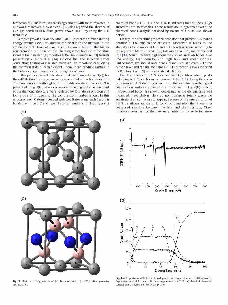
In this paper a zinc-blende structured like diamond (Fig. 3(a)) forthe c-BC2N thin films is expected as is reported in the literature [35].This configuration with eight-atom zinc-blende structured c-BC2N ispresented in Fig. 3(b), where carbon atoms belonging to the inner partof the diamond structure were replaced by four atoms of boron andfour atoms of nitrogen, so the coordination number is four. In thisstructure, each C atom is bonded with two B atoms and each B atom isbonded with two C and two N atoms, resulting in three types of
Fig. 3. Unit cell configurations of (a) Diamond and (b) c-BC2N after geometryoptimization.
chemical bonds: C–C, B–C and B–N. It indicates that all the c-BC2Nstructures are metastables. These results are in agreement with thechemical bonds analysis obtained by means of XPS as was shownbefore.
Clearly, the structure proposed here does not present C–N bondsbecause of the zinc-blende structure. Moreover, it tends to thestability as the number of C–C and B–N bonds increase according tothe reports of Mattesini et al [36], Tateyama et al [37], and Nozaki andItoh [38]. Structures with higher quantity of C–C and B–N bonds havelow energy, high density, and high bulk and shear modulii.Furthermore, we should note here a “sandwich” structure with thecarbon layer and the BN layer along b111N direction, as was reportedby X.F. Fan et al. [39] in theatricals calculations.
Fig. 4(a) shows the AES spectrum of BC2N films where peaksbelonging to B, C, and N can be observed. In Fig. 4(b) the depth profileis presented. AES depth profiles of all the samples revealed goodcomposition uniformity overall film thickness. In Fig. 4(b) carbon,nitrogen and boron are shown, decreasing as the etching time wasincreased. Nevertheless, they do not disappear totally when thesubstrate of silicon began to appear, because of the interdiffusion ofBC2N on silicon substrate. It could be concluded that there is acomposed interface between the film and the substrate. Otherimportant result is that the oxygen quantity can be neglected since
Fig. 4. AES spectrum of BC2N thin film deposited at a laser influence of 200 m J/cm2, adeposition time of 1 h and substrate temperature of 450 °C (a) chemical elementalcomposition analyses and (b) Depth profile.

Fig. 6. (a) TEM image in electron diffraction mode for BC2N thin films grown at 450 °C
4055H.A. Castillo et al. / Surface & Coatings Technology 204 (2010) 4051–4056
it remains close to zero. This is an evidence of the cleaning process andthe high vacuum reached before the films grown. On the other hand,from the depth profiles, an estimation of the sputtering rate of (1.61±0.14) nm/min was obtained, in agreement with the perfilometrymeasurements, where thicknesses were in the order of 480±4 nm. Itmeans that several monolayers per minute were sputtered. The filmsthickness (oscillating between 476 and 486 nm) does not havesignificant changes as a function of the temperature.
In order to probe the existence of the cubic phase, XRD patterns(Fig. 5) for samples grown at substrate temperatures of 350, 450, 550and 650 °C were taken. Difractograms showed the presence of (111),(200) and (220) planes belonging to c-BC2N. Although the diffractionpattern could also be interpreted as cBN, the stoichiometry analysiscarried out XPS and the AES results indicate the presence of c-BC2N.Moreover, a peaks shifting toward lower angles was observed. Resultsof Table 1 show an increase in the boron and carbon remainingnitrogen almost constant, as the substrate temperature was increased.It could produce an increase in the film density, in the latticeparameter and in the films stress, affecting the interplane distance[40,41]. Moreover, the amorphous BC2N was transformed into thecubic phase similar to diamond and c-BN at substrate temperaturegreater than 450 °C. Similar diffraction peaks of (111), (200) and(220) planes, were reported by S. Nakano et al [42] and Sasaki et al[43]. Furthermore, as the temperature was increased, c-BC2N peaks of(111), (200) and (220) planes became higher. A profile analysis of(200) and (220) lines did not reveal overlapping or asymmetric peaks.The calculated c-BN lattice parameter was 3.593 A, being in a goodagreement with the corresponding value (3.589 A ) found for c-BC2N.(111), (200) and (220) diffraction peaks [43] were corroborated byusing TEM in electron diffraction mode, as is shown in Fig. 6. In thisfigure the interplanar spacing was determined and compared withvalues reported by other authors. The values of lattice parameter andinterplanar distance are very close to those reported in theoreticalworks by J. Widany et al. [44]. They considered basically that thereduction in the BC2N lattice parameter compared with c-BN, or theincrease with respect to diamond, must be caused by the bondslongitude difference. For example, C–C bonds in the diamondstructure are shorter that B–N bonds in c-BN structure.
Fig. 6(b) presents a HRTEM image of c-BC2N crystallites. Thesecrystallites have also been identified on the basis of two-dimensionallattice fringes together with their corresponding angle, produced by
Fig. 5. XRD patterns of the samples obtained at different substrate temperatures.
and (b) HRTEM image of c-BC2N crystallites.
the (111) orientations. As is observed in this figure, the interplanarspacing d(111) is little greater than it reported for the diamond [45]and little lower than it for c-BN [46]. Finally, crystallites size wasestimated larger than 10 nm.
Regarding to hardness and in order to analyze the nanoindentationmeasurements for cubic BC2N, the Oliver and Pharr report [47] wasused. The resultant Young’s modulus was determined by:
1Er
=1−v2
E+
1−v2iEi
ð2Þ
where E and ν are the Young's modulus and the Poisson ratiorespectively. Ei and νi are the parameters for the diamond indenter(Ei=1141 GPa and νi=0.07 [47]. The c-BC2N young's modulus wascalculated from Eq. (2), using the value found experimentally(Er=309 Gpa) and under the assumption that the Poisson ratio ofc-BC2N is ν=0.096, calculated for the ideal mixing of diamond(diamond ν=0.07 [47] and cubic boron carbonitride ν=0.121 [48]).In our combined experimental and theoretical results, an increase inthe hardness of BC2N films as a function of the substrate temperaturewas observed as is shown in Fig. 7, especially for temperatures greaterthan 350 °C. According to TEM and XRD analysis, as substratetemperature increases, films tend to the crystallization. This

Fig. 7. Hardness behavior as a function of the substrate temperature.
4056 H.A. Castillo et al. / Surface & Coatings Technology 204 (2010) 4051–4056
crystallization also enhances the hardness [49], because of theincrease in the atomic density of the material as a consequence ofthe higher compactness of the zinc-blende structure. Also hardness isincreased as the cubic structure is achieved because of the strongerbonds (B–C, B–N y C–C), although it depends little on the atomicarrangements of the crystal structure [50].
Hardness is not as higher as was expected. Nevertheless, it isgreater than other coatings that normally are used in similarapplications as ZrN and WC [51,52]. Moreover, works carried out byM. J. Albella’s group (32 Gpa) [13] present hardness in the same orderand even lower (18 Gpa) [53] than those reported here. Thesedifferences in the hardness are due to this type of material would besignificantly affected by the nitrogen concentration.
By the hardness calculation, it was established that structures with(111) preferential orientations are harder than c-BN. Thus there havebeen active debates on whether bulk BCxN would have intermediatehardness between diamond and c-BN [39]. Moreover, among thetheoretical calculations carried out so far, it is found that manymechanical and electronic properties of BCxN are sensitive to theatomic arrangements and substitution patterns.
4. Conclusions
Cubic BC2N thin films were produced by using an Ablation Lasersystem varying the substrate temperature. These films were charac-terized by the XPS, AES, XRD, TEM and nanoindentation techniques. Insummary, B–N, B–C, and C–C chemical bonds can be identified fromthe XPS analysis without finding C–N bonds. By means of AES, depthprofiles were carried out, allowing exploring the films chemicalcomposition as a function of the thickness. With this analysis thepresence of C, B and N was found and also interdiffusion between thefilm and substrate was observed. XRD analyses showed that the thinfilms growth in this experiment possess an ordered structure,suggesting the existence of a zinc-blende structure with diffractionpeaks belonging to (111), (200) and (220) crystallographic planes,similar to c-BN and diamond. These planes were also observed bymeans of TEM. The hardness measured by using a Berkovich indenterpresented an increase as a function of the substrate temperature.
Acknowledgments
This work was partially support by projects CONACyT (México)50203-F and COLCIENCIAS (Colombia) RC566-2008. The authors are
grateful to F. Ruiz, D. Domínguez, E. Aparicio, I. Gradilla, E. Sámano andJ. Díaz for technical assistance.
References
[1] A. Bartl, R. Haubner, B. Lux, Int. J. Refract. Met. Hard Mater. 14 (1996) 145.[2] V.L. Solozhenko, S.N. Dub, N.V. Novikov, Diamond Relat. Mater. 10 (2001) 2228.[3] T. Kar, M. Cuma, S. Scheiner, J. Mol. Struct. 556 (2000) 275.[4] M. Watanabe, T. Sasaki, S. Itho, M. Mizushima, Thin Solid Films 281–282 (1996)
334.[5] D. Kurapov, D. Neuschutz, R. Cremer, T. Pedersen, M.Wutting, D. Dietrich, G. Marx,
J.M. Schneider, Vacuum 68 (2003) 335.[6] S. Ulrich, H. Ehrhard, T. Theel, J. Schwan, S. Westermeyr, M. Scheib, P. Becker, H.
Oechsner, G. Dollinger, A. Bergmaier, Diamond Relat. Mater. 7 (1998) 839.[7] A.R. Badzian, Mater. Res. Bull. 16 (1981) 1385.[8] Y. Kusano, J.E. Evetts, I.M. Hutchings, Thin Solid Films 343–344 (1999) 250.[9] H. Yasui, Y. Hirose, K. Awazu, M. Iwaki, Colloids Surf. B Biointerfaces 19 (2000)
291.[10] I. Caretti, I. Jiménez, R. Gago, D. Caceres, B. Abendroth, J.M. Albella, Diamond Relat.
Mater. 13 (2004) 1532.[11] Z. Ren, Y. Du, Z.F. Ying, F. Li, J. Lin, Y. Ren, X. Zong, Mater. Chem. Phys. 50 (1997) 98.[12] W.J. Pan, J. Sun, H. Ling, N. Xu, Z.F. Ying, J.D. Wu, Appl. Surf. Sci. 218 (2003) 297.[13] R. Gago, I. Jimenez, I. Garcia, J.M. Albella, Vacuum 64 (2002) 199.[14] Fei Zhou, Koshi Adachi, Koji Kato, Thin Solid Films 497 (2006) 210.[15] R. Gago, I. Jimenez, J.M. Albella, Thin Solid Film 373 (2000) 277.[16] J. Widany a, W.S. Verwoerd a, Th. Frauenheim, Diamond Relat. Mater. 7 (1998)
1633.[17] H.S. Kim, I.H. Choi, Y.J. Baik, Surf. Coat. Technol. 133–134 (2000) 473.[18] G. Soto, W. de la Cruz, M.H. Farıas, J. Electron. Spectrosc. Relat. Phenom. 135
(2004) 27.[19] D.B. Chrisey, G.K. Hubler (Eds.), Pulsed Laser Deposition of Thin Films, Wiley, New
York, 1994.[20] C. Vivien, M. Dinescu, P. Meheust, C. Boulmer-Leborgne, A.P. Caricato, J. Perriere,
Appl. Surf. Sci. 127–129 (1998) 668.[21] J. Wu, Z.F. Sun, Ying, et al., J. Vac. Sci. Technol. A19 (2001) 299.[22] J.H. Scofield, J. Electron. Spectrosc. 8 (1976) 129.[23] S. Jacques, A. Gguette, X. Bodrrat, F. Langlais, C. Guimon, C. Labrujere, Carbon 34
(1996) 1135.[24] F. Zhou, K. Adachi, K. Kato, Thin Solid Films 497 (2006) 210.[25] C. Kunz, E. E.koch, G.K. Wertheim, H. Hochst, L. Ley, M. Campagna, M. Cardona, P.
Steiner, R.A. Pollak, S. Hufner, W.D. Grobman, Y. Baer, in: L. Ley, M. Cardona (Eds.),Topics in Applied Physics, Vol 27, Springer-Verlag, Berlin Heidelberg New-York.N° Publi: (1979) 147.
[26] S. Inoue, K. Tominaga, R.P. Howson, K. Kusaka, J. Vac, Sci. Technol. A. 13 (1995)2808.
[27] S. Jacques, A. Gguette, X. Bodrrat, F. Langlais, C. Guimon, C. Labrujere, Carbon 34(1996) 1135.
[28] E. Pascual, E. Martínez, J. Esteve, A. Lousa, Diamond Relat. Mater. 8 (1999) 402.[29] J. Yue, W. Cheng, X. Zhang, D. He, G. Chen, Thin Solid Films 375 (2000) 247.[30] C. Morant, P. Prieto, J. Bareño, J.M. Sanz, E. Elizalde, Thin Solid Films 515 (2006)
207.[31] M.K. Lei, Quan Li, Z.F. Zhou, I. Belloa, C.S. Lee, S.T. Lee, Thin Solid Films 389 (2001)
194.[32] Y. Wada, Y.K. Yap, M. Yoshimura, Y. Mori, T. Sasaki, Diamond Relat. Mater. 9
(2000) 620.[33] Wenying Zhoua, Shuhua Qi, Haidong Li, Shiyu Shao, Thermochimica Acta 452
(2007) 36.[34] Y. Mori, M. Tanemura, S. Tanemura, Appl. Surf. Sci. 228 (2004) 292.[35] J. Widany, W.S. Verwoerd, Th. Frauenheim, Diamond Relat. Mater. 7 (1998) 1633.[36] M. Mattesini, S.F. Matar, Comput. Mater. Sci. 20 (2001) 107.[37] Y. Tateyama, T. Ogitsu, K. Kusakabe, S. Tsuneyuki, S. Itoh, Phys. Rev. B 55 (1997)
10161.[38] H. Nozaki, S. Itoh, Phys. B 219–220 (1996) 487.[39] X.F. Fan, H.Y. Wu, Z.X. Shen, Jer-Lai Kuo, Diamond Relat. Mater. 18 (2009) 1278.[40] S.H. Park, J.H. Chang, H.J. Ko, T. Minegishi, J.S. Park, I.H. Im, M. Ito, D.C. Oh, M.W.
Cho, T. Yao, Appl. Surf. Sci. 254 (2008) 7972.[41] D.F. Arias, Y.C. Arango, A. Devia, Appl. Surf. Sci. 253 (2006) 1683.[42] S. Nakano, M. Akaishi, T. Sasaki, S. Yamaoka, Mater. Sci. Eng. A209 (1996) 26.[43] T. Sasaki, M. Akaishi, S. Yamaoka, Y. Fujiki, T. Oikawai, Chem. Mater. 5 (1993) 695.[44] J. Widany, W.S. Verwoerd, Th. Frauenheim. Diamond Relat. Mater. 7 (1998) 1633.[45] Dieter M. Gruen, Annu. Rev. Mater. Sci. 29 (1999) 211.[46] Gang Lian, Xiao Zhang, Lingling Zhu, Deliang Cui, QilongWang, Xutang Tao, J. Solid
State Chem. 182 (2009) 1326.[47] W.C. Oliver, G.M. Pharr, J. Mater. Res. 7 (1992) 1564.[48] M. Kawaguchi, Adv. Mater. 9 (1997) 615.[49] G. Zhang, H. Liao, H. Yu, V. Ji, W. Huang, S.G. Mhaisalkar, C. Coddet, Surf. Coat.
Technol. 200 (2006) 6690.[50] X. Guo, Z. Liu, X. Luo, D. Yu, J. He, Y. Tian, J. Sun, H-T. Wang, Diamond Relat, Mater.
16 (2007) 526.[51] M.A. Auger, J.J. Araiza, C. Falcony, O. Sánchez, J.M. Albella, Vacuum 81 (2007) 1462.[52] C. Larsson, M. Odén, Mater. Sci. Eng. A 382 (2004) 141.[53] I. Caretti a, J.M. Albella a, I. Jiménez, Diamond Relat. Mater. 16 (2007) 63.

ARTICLE IN PRESS
0026-2692/$ - se
doi:10.1016/j.m
�CorrespondE-mail addr
Microelectronics Journal 39 (2008) 1382–1384
www.elsevier.com/locate/mejo
Electron inelastic mean free path for B4C and BC2N determinedby reflection electron energy loss spectroscopy
H.A. Castilloa,�, A. Deviab, G. Sotoc, J.A. Dıazc, W. De La Cruzc
aPosgrado en Ciencias y Tecnologıa de Materiales, Universidad Nacional de Colombia Sede Manizales, ColombiabLaboratorio de Fısica del Plasma, Universidad Nacional de Colombia Sede Manizales, Colombia
cCentro de Ciencias de la Materia Condensada, Universidad Nacional Autonoma de Mexico, A. P. 2681, C.P. 22860 Ensenada, B.C., Mexico
Available online 17 March 2008
Abstract
Amorphous B4C and BC2N films were prepared on (1 1 1) silicon substrates by reactive laser ablation using a B4C target. For the
depositions of BC2N a nitrogen pressure of 63mTorr in the growth chamber was used. The electron inelastic mean free path (IMFP) for
B4C and BC2N was calculated for energies between 200 and 2000 eV from their respective energy-loss functions, which was obtained
from quantitative analysis of REELS. The IMFPs are analyzed in terms of the Bethe equation for inelastic scattering of electron. REELS
results were used to obtain the dielectric function of the B4C and BC2N in the energy range from 4 to 100 eV.
r 2008 Elsevier Ltd. All rights reserved.
PACS: 79.20.Kz
Keywords: IMFP; B4C; BC2N; REELS; Electron spectroscopies
1. Introduction
An important parameter for quantitative analysis usingsurface electron spectroscopies is the electron inelasticmean free path (IMFP). Usually the IMFP values for somematerials are obtained from the energy-loss function(ELF), which is obtained from optical data. These IMFPvalues can be reproduced using the TPP-2M predictiveequation proposed by Tanuma et al. [1]. This procedurerelies on accessible and trustworthy optical data over wideranges of energy; this is seldom the case when studying newmaterials. Consequently it is indispensable to devise newmethods to obtain IMFP values, if possible by usingcurrently available analysis method. The aim of this workis to determine the IMFPs using ELFs derived fromreflection electron energy loss spectroscopy (REELS)measurement. The methodology is applied to study B4Cand BC2N compounds.
e front matter r 2008 Elsevier Ltd. All rights reserved.
ejo.2008.01.082
ing author.
ess: [email protected] (H.A. Castillo).
2. Experimental
Boron carbon nitride films were accomplished byablating a high purity B4C, 99.9wt%. Films were grownon (1 0 0)-silicon wafers at room temperature in an ultra-high vacuum system with a base pressure of 10�9 Torr.Target ablation was performed by means of a KrF excimerlaser (l ¼ 248 nm). Laser energy, deposition time and pulserepetition rate are fixed at 400mJ (nominal), 60min and5Hz, respectively. B4C films were grown at high vacuumconditions, while a mixture of N2 (60mTorr) þ CH4
(3mTorr) during the ablation was used to obtain BC2Nstoichiometric thin films. These films were analyzed in situby X-ray photoelectron spectroscopy and REELS. Thestoichiometries of the films were obtained from XPS.REELS spectra were taken at three primary electronenergies (Ep) of 0.5, 1.0 and 1.5 keV. The method forobtaining the dielectric function consists of comparingtheoretical and experimental electron inelastic cross-sec-tions determined at Ep; details from this procedure are inthe Ref. [2]. This formalism has been applied successfully toobtain information about the inelastic scattering properties

ARTICLE IN PRESSH.A. Castillo et al. / Microelectronics Journal 39 (2008) 1382–1384 1383
of thin films and solids, as well as to estimate the IMFPsfor several elements and compounds [3].
3. Results and discussions
Fig. 1 shows the experimental inelastic cross-sections inthe form Kexp (square) for B4C and BC2N. They have beenobtained from REELS spectra measured at 500, 1000 and2000 eV primary electron energies, after normalization tothe area of the elastic peak and removal of multipleinelastically scattered electrons. Fig. 1 also includes therespective theoretical inelastic scattering cross-sections K th
(lines), calculated according to the procedure described inRef. [2]. The agreement between K th and Kexp for the three
0.06
0.04
0.02
0.00
0.06
0.04
0.02
0.00
0.06
0.04
0.02
0.00
0 20 40 60 80 100
0 20 40 60 80 100
0 20 40 60 80 100
B4C
Fig. 1. Experimental inelastic scattering cross-sections (square) at three primary
lines) for B4C (left side) and BC2N (right side).
40
30
20
10
00 1000 2000
Energy (eV)
IMFP
(Å)
Fig. 2. lREELS (squares) and l1 (full lines) determined in this study as a fu
included. The data showed inside of the figure are the Bethe parameters (see E
different Ep is rather good, taking into account that thecomparison is performed on an absolute scale. In addition,ELFs proposed for obtaining the K th were used to calculateelectron IMFPs for each material in the 200–2000 eVenergy range.Fig. 2 shows the values for lREELS (squares, it is when the
IMFPs were calculated taking into account the effects ofsurface) and l1 (full lines, it is when the IMFPs werecalculated in the bulk) calculated for B4C and BC2N, aslabeled. The difference among those IMFPs is about0.1 nm for the materials studied. For comparison, theTPP-2M values obtained from Eq. (1) have been plotted asdashed lines in the respective figures. It is possible toobserve that IMFPs from TPP-2M have a difference of up
0.04
0.02
0.00
0.04
0.02
0.00
0.04
0.02
0.00
0 20 40 60 80 100
0 20 40 60 80 100
0 20 40 60 80 100
BC2N
energies (as labeled) and theoretical inelastic scattering cross-sections (full
40
30
20
10
00 1000 2000
Energy (eV)
nction of energy. For comparison, the TPP2M values (dashed lines) are
q. (1)).

ARTICLE IN PRESSH.A. Castillo et al. / Microelectronics Journal 39 (2008) 1382–13841384
to 50% with the values obtained for lREELS and l1. Thedata were fitted to Eq. (1), known as Bethe equation,obtaining the parameters shown in Fig. 2.
lðE0Þ ¼E0
E2PbðlnE0 þ ln gÞ
. (1)
4. Conclusions
Electron energy-loss functions of B4C and BC2N in theenergy range 3–90 eV have been determined from experi-mental REELS spectra. The differences between lREELS
and l1 are observed to be 0.1 nm for the materials studiedhere. IMFPs calculated by the TPP-2M formula showdifferences of up to 50% with respect to IMFPs calculatedfrom REELS spectra.
Acknowledgments
The authors are grateful to E. Aparicio, V. Garcıa, P.Casillas and J. Peralta for technical assistance. This workwas partially support by projects DGAPA IN120306 andCONACyT 50203-F.
References
[1] S. Tanuma, C.J. Powell, D.R. Penn, Surf. Interface Anal. 25
(1997) 25.
[2] F. Yubero, J.M. Sanz, B. Ramskov, S. Tougaard, Phys. Rev. B 53
(1996) 9719.
[3] F. Yubero, J.M. Sanz, J.F. Trigo, E. Elizalde, S. Tougaard, Surf.
Interface Anal. 22 (1994) 124.