synthesis and microstructural characterization of...
TRANSCRIPT
Chapter 2
SYNTHESIS AND MICROSTRUCTURAL CHARACTERIZATION OF NANOSTRUCTURED MATERIALS
2.1. Introduction
Artificially synthesized nanostructured materials have structures in zero to
three dimensions. Nanostructured materials thus include zero dimensionality atom
clusters and cluster assemblies, one dimensionally modulated multilayers, and their
three-dimensional analogues, nanophase materials.' There are three key steps in the
development of nanoscience and nanotechnology: materials preparation, property
characterization, and device fabrication. Preparation of nanomaterials is being
advanced by numerous physical and chemical techniques. The purification and size
selection techniques developed can produce nanocrystals with well-defined
structure and morphology.2s3 Due to size and structure selectivity of nanomaterials,
the physical property of nanomaterials could be quiet diverse. It is known that the
properties of nanostructures depend strongly on their size and
The synthesis of nanostructured materials (NSMs) from atomic or molecular
sources depends on the control of a variety of "nanoscale" attributes desired in the
final product. The first technique involves the production of isolated, ultrafine
crystallites having uncontaminated free surfaces followed by a consolidation
process either at rooni temperature or at elevated temperatures.6 Nanocomposites
can be produced by depositing chemically different molecules simultaneously or
consecutively.' By introducing defects in a formerly perfect crystal such as
dislocations or grain boundaries, new classes of NSMs can be synthesized.
Different physical methods are currently in use for the synthesis and
commercial production of NSMs. The first and most widely used technique
involves the synthesis of single-phase metals and ceramic oxides by the inert-gas
evaporation technique. The evaporated atoms or molecules undergo a homogeneous
condensation to form atom clusters via collisions with gas atoms or molecules in
the vicinity of a cold - powder collection surface. The clusters once formed must be
removed from the region of deposition to prevent further aggregation and
Chapter 2 28
coalescence of the cluster^.^" Sputtering is another technique to produce NSMs as
well as a variety of thin films. This method involves the ejection of atoms or
clusters of designated materials by subjecting them to an accelerated and highly
focused beam of inert gas such as argon or helium. The third physical method
involves the generation of NSMs via severe mechanical deformation. In this
method, NSMs are produced by structural degradation of coarser-grained structure5
induced by the application of high mechanical energy. The nanometer-sized grains
nucleate within the shear bands of the deformed materials converting a coarser-
grained structure to an ultrafine powder. The heavy deformation of the coarser
material is effected by means of a high-energy ball mill or by a high-energy shear
stress process. 6-8
Chemistry has played a major role in developing new materials with novel
and technologically important properties. The advantage of chemical synthesis is its
versatility in designing and synthesizing new materials that can be refined in to the
final product. The primary advantage that the chemical process offer over other
methods is good chemical homogeneity, as chemical method offers mixing at
molecular leveLg A basic understanding of the principles of crystal chemistry,
thermodynamics, phase equilibrium, and reaction kinetics is important to take
advantage of the many benefits that chemical processing has to offer.
Solution chemistry is used sometimes to prepare the precursor, which i s
subsequently converted to the nanophase particles by nonliquid phase chemical
reactions. Precipitation of a solid from a solution is a common technique for the
synthesis of fine particles. The growth of the nuclei after formation usually
proceeds by diffusion, in which case concentration gradient and reaction
temperatures are very important in determining the growth rate of the particles. For
instance, to prepare unagglomorated particles with a very narrow size distribution,
all the nuclei must form at flearly the same time and subsequent growth must occur
without further nucleation Zr agglomeration of the particles.1° The particle size and
stze distribution, the physical properties such as crystallinity and crystal structure,
the degree af dispersion etc. ciul be affected by reaction In addition, the
concentratiorr of reaLtants, the reaction temperature, the pH and the order of
Synthesis and Microstrucrur~zl Characterization of Nanusrrucrured Mareriols 29
addition of reactants to the solution are also important.9-" Thus, chemical
homogeneity and stoichiomem/ requires a very careful control of reaction
conditions.
In this chapter, the synthesis of the nanocrystalline forms of aluminium
phosphate (AIP04), copper pyrophosphate (CuzP207). magnesium pyrophosphate
(MgzP207) and the nanocomposite magnesium pyrophosphate-iron phosphate
(Mg2P~07 - Fe3(P04)2) ancl their characterization details are presented. Each sample
is prepared in three different grain sizes by varying the molar concentration of the
reactants. The sintered samples are subjected to X-ray diffraction analysis, through
which the crystal structures, grain sizes and the changes in lattice parameters are
analyzed. The phase changes with temperature of nano Alp04 sample are studied
through transmission electron micrographs and selected area diffraction patterns.
2.2. Synthesis of Nanocrystalline Metal Phosphates
For the present study, nanocrystalline powders of three different metal
phosphates; namely a1u:niniunl phosphate (AlP04). copper pyrophosphate
(Cu2P207) & magnesium pyrophosphate (MgzPz07) were prepared in three different
grain sizes, by changing the molar concentration of the reactants. The
nanocomposite Mg2P207 - Fe3(P04)2 for different iron phosphate concentrations
were also prepared. All the samples were synthesized from a polymer matrix based
precursor solution through a versatile, efficient and technologically simple method.
A detailed description of the synthesis route is given in the literature.'' Analytical
grade (AR) chemicals of high purity were used for the synthesis of all samples in
the present study.
To produce nanociystalline aluminium phosphate (n-AIP04), aluminium
nitrate [A1(N03)2.9Hz0] (I moVlL HzO) is mixed with ammonium dihydrogen
phosphate [NH4(HzP04)] ( I moV 500 ml H20) and then with dilute HNO,, such that
pH of the solution = 1. To this mixture 3 moles of sucrose and 10% wlv aqueous
solution of PVA (0.05 mol:~ are added, so that the total volume of the solution after
mixing is 3.0 L. The solution is well stirred and then evaporated to a viscous liquid
with the evolution of brown fumes of the decomposed nitrates. The PVA is acting
as the matrix and sucrose as the fuel. The fluffy, voluminous, carbonaceous,
Chapter 2 30
pyrolysed mass produced during the complete evaporation of the precursor solution
of metal nitrate-PVA-sucrose is then thermolysed from room temperature to 900 'C
to get the nanosized powder. The resulting powder is then calcinated at 900 "C for 4
hours to obtain the crystalline phase of the required sample.lz Samples with
different grain sizes are prepared by changing the molar concentration of the
reactants." Molar concentrations of 1.0 mol~ . ' , 0.5 m o l ~ . ' and 0.1 m o l ~ . ' are
selected for the present study. The overall reaction can be represented as:
Aluminium phosphate (AIP04) thus formed becomes more crystalline and
nanosized under further heat treatments in presence of sucrose and PVA. The
ammonium nitrate (NH4 N03) decomposes to NH3 and NO2
Nanocrystalline copper pyrophosphate (n-CuzP207) and magnesium
pyrophosphate (n-Mg2P207:l are also prepared in a similar manner. Copper nitrate
[Cu(N03)~.3HzO] and magnesium nitrate [Mg(N03)~.6H201 are respectively used
instead of aluminium nitrate. Copper phosphate samples were calcinated at 600 OC
for 4 hours and magnesium phosphate samples were calcinated at 900 OC for 4
hours to get the required crystalline phase. The corresponding reactions are:
Copper phosphate I[Cu3(P04)2] and magnesium phosphate [Mg3(P04)2]
formed here transform to copper pyrophosphate (CUZPZO~) and magnesium1
pyrophosphate (Mg2P207) above 160°C. Ammonium nitrate (NHdNO3) decomposes
to NH3 and NOz.
The nanocomposite MgzP207 -Fe3(P04)2 with different weight percent of
iron phosphate (= 5%, lo%, & 15%) are prepared, for the present study, by mixing
freshly prepared n-Mg2P207 and n-Fe3(P04)z in an agate mortar and grounded well.
The method of synthesis of n-Fe3(P04)z is exactly similar t~ that descnbed above
for the other samples. The prepared samples were tnen calcinated at 900°C for 4
hours to obtain the desired clystalline phase.
Synthesis and Microstructural Characterization of Nanosrructured Materials 3 1
2.3. Consolidation of Nanoparticle Samples
In the fabrication of nanostmctured materials, full densification of the
powder is to be achieved while simultaneously retaining the nanoscale
microstructure. To reduce grain growth during sintering, a high-density
homogeneous sample with minimum pore size is required.I4 Thus, prior to sintering
a sample composed of nanosize powders, it is essential to compact the powder at
high pressures. For the present case, the nanopowder samples were consolidated in
the form of cylindrical pellets of 13 mm diameter and thickness about 1-2 rnm. For
micro hardness ~tudies, '~.~' a uniaxial force ranging 3-6 tons is applied for 2
minutes using a hand operated hydraulic press. For dielectric studies the uniaxial
force applied was 4 ton:$ for all the samples. Conducting silver paste was coated on
both faces of the pellets to serve as electrodes. The pellets were air heated at 80°C
for 30 minutes in a hot air oven for electrode c ~ r i n ~ . ' ~ . ~ ~
2.4. X-ray Diffraction (XRD) Analysis of Nanocrystalline Materials
Scattering and imaging techniques are usually employed to determine the
nature of nanoparticle crystal s t ~ c t u r e . ~ ' The versatile and most widely used
technique is X - ray diffraction and scattering. X -ray diffraction method is used as
a tool for the determination of the crystal structure, particle size and changes in the 22-24 lattice parameters of all the samples in the present investigation. When
clystallites are of nanometer size appreciable broadening in the X-ray diffraction
lines will occur. The observecl line broadening can be used to estimate the average
size of the particles. The diffraction patterns were recorded using a Philips
Analytical PW1710 BASED diffractometer. The X -ray generator was operated at
35 KV and at 20 mA. Copper K, (1 = 1.5418 A) radiation was used as source. The
'd' values obtained from XRD were compared with standard 'd' values obtained
from the Internarional Center for Drffraction Data - Powder Dljfraction Files
(ICDD - P D e . The expansion or contraction of the lattice due to reduction in the
physical dimension of all the crystalline samples is systematically analysed. The
particle sizes were determined through the line broadening of the diffraction lines
using Scherrer formula.2s
Chapter 2 - 32
X-ray diffraction techniques are widely accepted for the characterization of
small particles. Broadness and shape of the measured diffraction lines are
characteristic of the crystallite size of the sample. Very small crystallites can be
considered to be domains, which are diffracting incoherently with respect to one
another, resulting in line broadening.
Reduction in the physical dimension of a crystalline solid leads to changes
in the lattice parameters. The expansion or contraction of the lattice in nanocrystals
with reducing particle size depends primarily on the nature of the interatomic bonds'
(ionic, covalent or metallic).26 It is reported2' that the unit cell should contract with
decreasing particle size in ionic crystals. In covalent and metallic crystals, on the
other hand, a decrease in the particle size is accompanied by an increase in the
lattice parameters, leading to an enhancement in the unit cell volume. For cubic
lattices, a size dependent intra-crystalline pressure is observed due to the
electrostatic interaction between the atoms of the lattice. This interaction energy is
positive in certain crystals that contain ions with opposite charges in the atomic
planes parallel to the crystal axes. The interaction energy is negative in certain other
crystals due to the presence of Ions of like charges in atomic planes.
In covalent cubic crystals, there is a small expansion in the lattice parameter
with decreasing size. This is explained using a point charge modelz8, which predicts
that the magnitude of the size effect should be directly proportional to the square of
the excess negative charge localized on bond lines between neighboring atoms. The
ions in the outermost layer are incompletely coordinated and posses unpaired
electronic orbitals. Each of these dangling bonds forms an electric dipole, resulting
in a parallel array of dipoles originating in the boundary layer of each nanoparticle.
The repulsive inter-dipolar forces thus formed would tend to increase the
equilibrium values of lattice constants. The lattice expansion is also due to some
other reasons such as capping layers formation at the surface29 due to chemical
impurities, such as C, N, and 0 that penetrate into the surface and expand the
spacing between the atomic layers
Synthesis and Microsrructural' Characterization of Nanosrructured Materials 33
In nano crystalline materials, the surface atoms amount to 40.50% of the
total atoms depending on the geometry. Every atom on the particle surface
contributes half of its surface area to the whole surface area of nanoparticle. As a
result, the surface energy of nanoparticles decreases which will tend to contract
their sizes by distorting their crystal lattice elastically. The best description of
nanoparticle structure includes bond length contraction and random disorder3'
characterized by correlated. atomic displacements. Bond length contraction makes
the nanoparticles much stiffer than expected. It is well known that the lattice
constant of small particles is different from the bulk, owing to the existence of
surface or interface stress.31 Obviously; the variation of lattice constants will result
in a change of the electron density in the particles. Since, changes and disorder in ---- the lattice p w s will separately modify electronic properties, inclusion of
3 -
these effects is essential for accurate nanoparticle calculations. - ---
2.5. Results and Discussion
2.5 (i) XRD Analysis of Nanostructured Alp04
Nano-sized AIP04 (n-AIP04) samples of different grain sizes were prepared
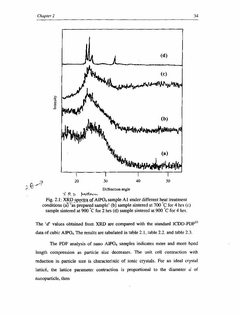
and the effects of thermal treatment on these powders were studied. Fig.2.1 presents
the XRD spectra of 'as prepared sample' and samples with different heat treatment
conditions. An examination of these spectra leads to the conclusion that the 'as
prepared sample' and samples at low heat treatment conditions are amorphous in
nature as shown in Fig.2.1 (a, b, c). The crystalline nature gradually increases as the
, annealing temperature and annealing time are increased. The broad bands 7 - corresponding to the annealing temperature at 9 0 0 ' ~ for 5 hours showiin Fig.2.l(d)
clearly indicate the crystalline nature of the sample at higher annealing conditions.
The mean crystallite sizes of the samples were determined using Schemer formula.
It is estimated that the average crystallite size of the sample is 16.34 nm. For the
present study nano-sized samples of Alp04 with average grain sizes of 16.34 nm, P.
13.59 nm and 12.04 nm, were prepared, by changing the concentration of the
reactants3' to 1.0 mol~- ' , 0.5 mol1;' and 0.1 mol~. ' (hereafter referred to as samples 1 Al , A2 & A3) respectively. Fig.2.2 shows the XRD pattern of all the three samples ---- I
1 of AIP04 prepared with different grain sizes. All the samples are of cubic structure.
r . Diffraction angle
* R D WWY AIP04 sample A1 under different heat treatment sample' (b) sample sintered at 700 'C for 4 hrs (c)
sample sintered at 900 OC' for 2 hrs (d) sample sintered at 900 'C for 4 hrs.
The '8 values obtained from XRD are compared with the standard ICDD-PDF)~
data of cubic Alp04 The results are tabulated in table 2.1, table 2.2. and table 2.3.
The PDF analysis of nano Alp04 samples indicates more and more bond
length compression as particle size decreases. The unit cell contraction with
reduction iri particle size is characteristic of ionic crystals. For an ideal crystal
lattick, the lattice parameter contraction is proportional to the diameter a of
nanoparticle, Lien

Synthesis and Microstructural Characterization of Nanosfrucfured Materials 35
Diffraction angle 2 ,? 5:
Fig.2.2 XRp spectraf nanocrystalline Alp04 samples (a) sample A 1 (b) sample A2 and (c) sample A3; sintered at 900 'C for 4 hrs.
Table 2.1 XRD pattern of nanocrystalline Alp04 sample Al
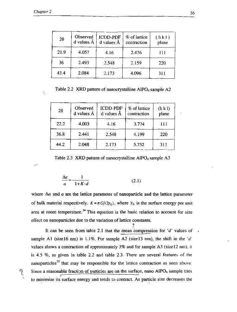
Table 2.2 XRD pattern of nanocrystalline Alp04 sample A2
of m a t t l ~ / d values A d values A contraction
Table 2.3 XRD pattern of nanocrystalline Alp04 sample A3
where Aa and a are the lattice parameter of nanoparticle and the lattice parameter
of bulk material respectively. K =xG/ (2y0) , where yo is the surface energy per unit
area at room temperature.34 This equation is the basic relation to account for size
effect on nanoparticles due to the variation of lattice constants. 1 f ,
It can be seen from tahle 2.1 that the mean compression for 'd' values of --- sample A1 (size16 nm) is 1.1%. For sample A2 (size13 nm), the shift in the 'd'
values shows a contraction of approximately 3% and for sample A3 (size12 nm), i t
is 4.5 %, as given in table 2.2 and table 2.3. There are several features of the
nan~~art ic les '~ that may be responsible for the lattice contraction as seen above
Since a reasonable fractim af wirticles are on the surface, nano ALP04 sample tnes 7 -- -
to minimize its surface energy and tends to contract. As particle size decreases the
Synthesis and Microstructural Characterization of Nanostructured Materials 37
percentage of surface atoms increases, which explains the increase in lattice
compression as particle size decreases. Opposite charges located in atomic planes
parallel to the crystal axes of nano Alp04 samples give a positive electrostatic
interaction between the elements of the lattice. The intra-crystalline pressure36 thus
produced is also responsible for the contraction of lattice parameters observed in
nanocrystalline Alp04 samples.
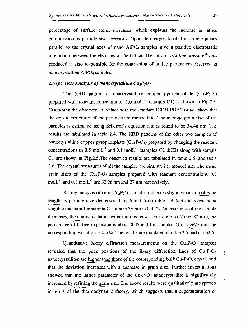
2.5 (ii) XRD Analysis of'Nanocrystalline CuzPz07
The XRD pattern of nanocrystalline copper pyrophosphate (Cu2P207)
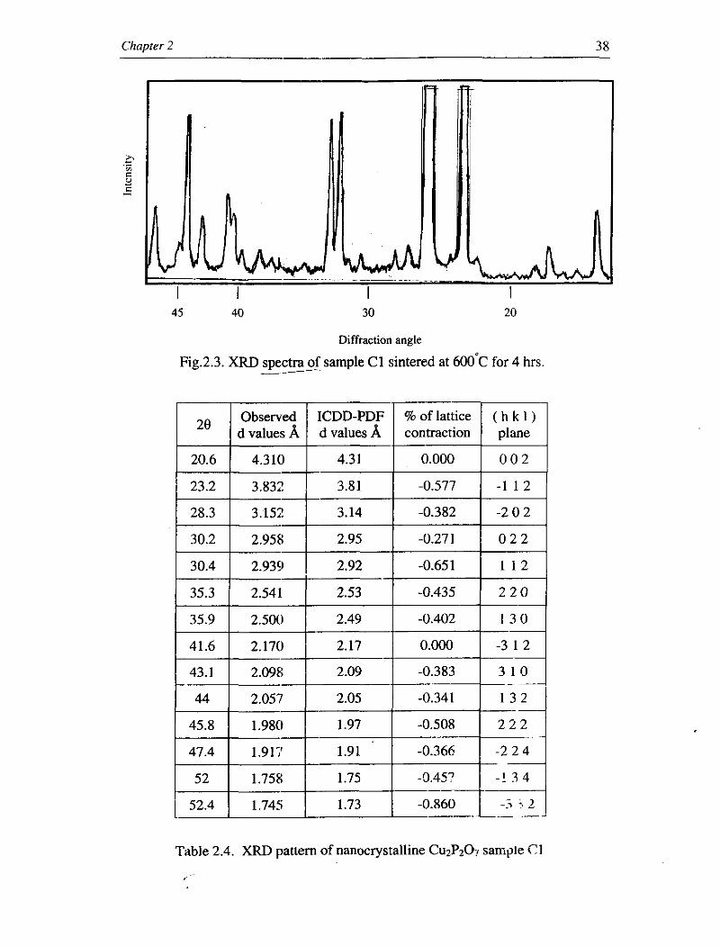
prepared with reactant concentration 1.0 molL-' (sample C1) is shown in Fig.2.3.
Examining the observed 'd' values with the standard ICDD-PDF~~ values show that
the crystal structures of the particles are monoclinic. The average grain size of the
particles is estimated using Schemer's equation and is found to be 34.46 nm. The
results are tabulated in table 2.4. The XRD patterns of the other two samples of
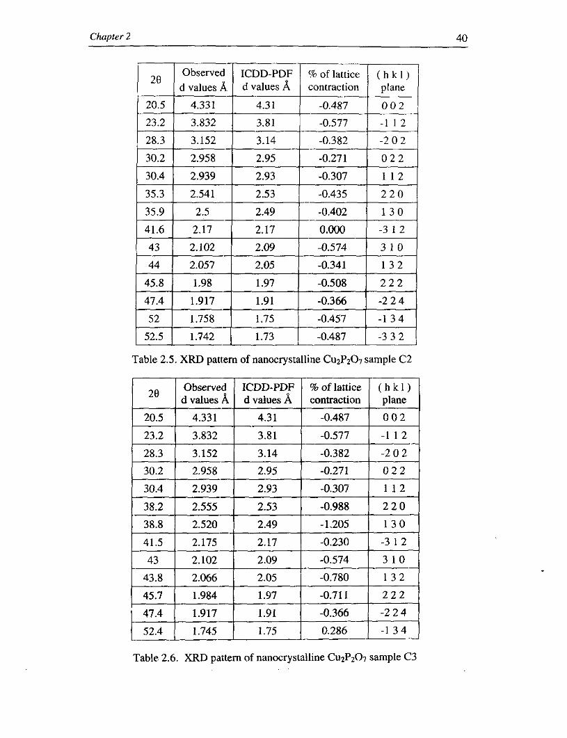
nanocrystalline copper pyrophosphate (Cu2P207) prepared by changing the reactant
concentrations to 0.5 molL-' and 0.1 m o l ~ . ' (samples C2 &C3) along with sample
C1 are shown in Fig.2.58.The observed results are tabulated in table 2.5. and table
2.6. The crystal structures of all the samples are similar; i.e. monoclinic. The mean
grain sizes of the Cu~Pz07 samples prepared with reactant concentrations 0.5
mo l~ . ' and 0.1 mol~ . ' are 32.26 nm and 27 nm respectively.
X - ray analysis of nano CuzPz07 samples indicates slight expansion of bond
length as particle size decreases. It is found from table 2.4 that the mean bond - length expansion for sample C1 of size 34 nm is 0.4 %. As grain size of the sample
decreases, the degree of lattice expansion increases. For sample C2 (size32 nm), the ?
--- percentage of lattice expansion is about 0.45 and for sample C3 of size27 nm, the -- -- corresponding variation is 0.5 %. The results are tabulated in table 2.5 and table2.6.
Quantitative X-ray diffraction measurements on the Cu~P207 samples
revealed that the peak. positions of the X-ray diffraction lines of Cu~P207 I nanocrystallites are higher than those of the corresponding bulk CuzP207 crystal and
7--
that the deviation increases with a decrease in grain size. Further investigations
showed that the lattice parameter of the Cu2P207 nanocrystallite is significantly
increased by refining the grain size. The above results were qualitatively interpreted 1
_C_-
in terms ot the thermodynanuc theory, which suggests that a supersaturation of
Diffraction angle
Fig.2.3. XRD spectra of sample C1 sintered at 6 0 0 ' ~ for 4 hrs -- Observed ICDD-PDF % of lattice ( h k I ) 1 2e 1 d values b / d values b / contraction I plane 1
Table 2.4. XRD pattern of nanocrystalline Cu2P207 sample ('1

Synthesis and Microstructural Characterization of Nanostructured Materials 39
X * .- 2 Y c -
I 60
I 50
I 40
I 30
I 20
Diffraction angle - d e ?'
Fig.2.4. XRD spectraof nanocrystalline C U ~ P Z O ~ samples (a) sample C1 sintered at 600 'C fo;2 hrs (b) sample C1 (c) sample C2 and (d) sample C3; sintered at 600 'C
for 4 hrs
Chapter 2 40
) , B p G G d J I C D D - P D r V l d values A, d values A contraction
Table 2.5. XRD pattern of nanocrystalline Cu2Pz07 sample C2
Obsewed I ICDD-PDF % of lattice ( h k 1 ) I 2B I d values A c~ vaiues A I contraction I plane I
Table 2.6. XRD pattern of nanocrystalline Cu2P207 sample C3
Synthesis and Microstructural Characterization qf Nanostructured Materials 41
vacancies in the lattice structure of a nm-grained system is obtained as the grain
size is decreased down to a few nanometres. 38
Lattice variations and bonding characteristics in Ti02 nanocrystals were
examined39 by x-ray diffraction spectroscopy. With a reduction in the physical
dimensions, Ti02 nanocrystals show a linear lattice expansion and an anomalous
covalency enhancement. A surface defect dipole model is proposed to explain these
physical phenomena in terms of the strong interactions among the surface dipoles
that produce an increased negative pressure. The covalency enhancement is
interpreted according to the critical properties of the increased Ti-0 bond lengths in
the expanded lattice.
The observation of lattice expansion of Cu2P207 nanocrystallite is in perfect
agreement with this theory. The broadening of the strong P-0 and the weak Cu-0
bands of nanocrystalline CuzPz07 samples are observed by FTIR analysis as
described in section 3.2 (ii). In covalent crystals, as explained in section 2.5, unit
cell volume increases as particle size decreases, which is accompanied by an
increase in the lattice parameters.28 Nanocrystalline Cu2P207 showing a similar
character may thus be considered as a covalent crystal. The ions in the outermost
layer of covalent crystals are incompletely coordinated and these dangling bonds
form an electric dipole of the same character in the boundary layer of each
nanoparticle. The repulsive inter-dipolar forces thus formed increases the
equilibrium values of lattice constants. Capping layers formation at the surface due
to chemical impuritiesz9 is also responsible for lattice expansion in nano CuzP207,
2.5 (iii) XRD analysis of nanocrystalline MgzPzO,
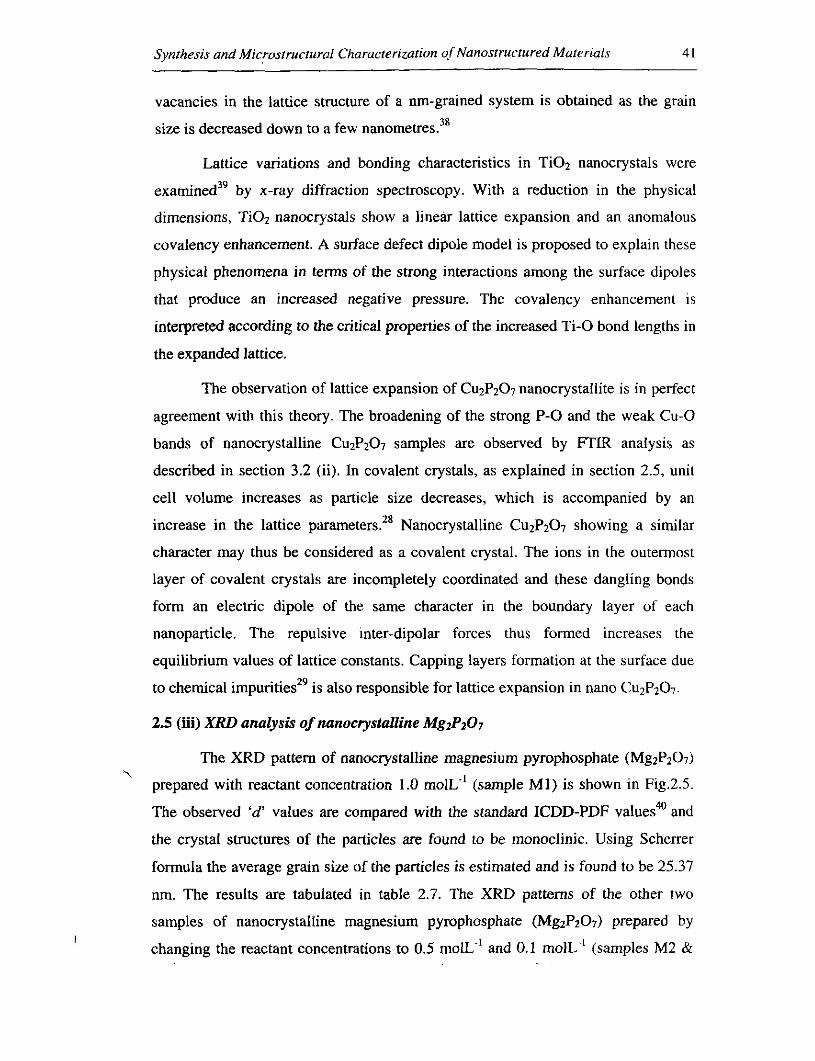
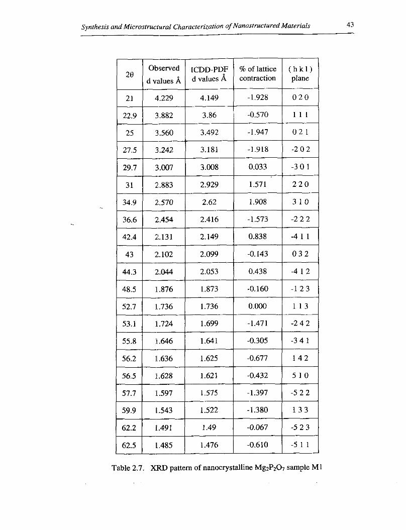
The XRD pattern of nanocrystalline magnesium pyrophosphate (MgzPz07)
prepared with reactant concentration 1.0 mol~. ' (sample MI) is shown in Fig.2.5.
The observed 'd' values are compared with the standard ICDD-PDF values4' and
the crystal structures of the particles are found to be monoclinic. Using Scherrer
formula the average grain size of the particles is estimated and is found to be 25.37
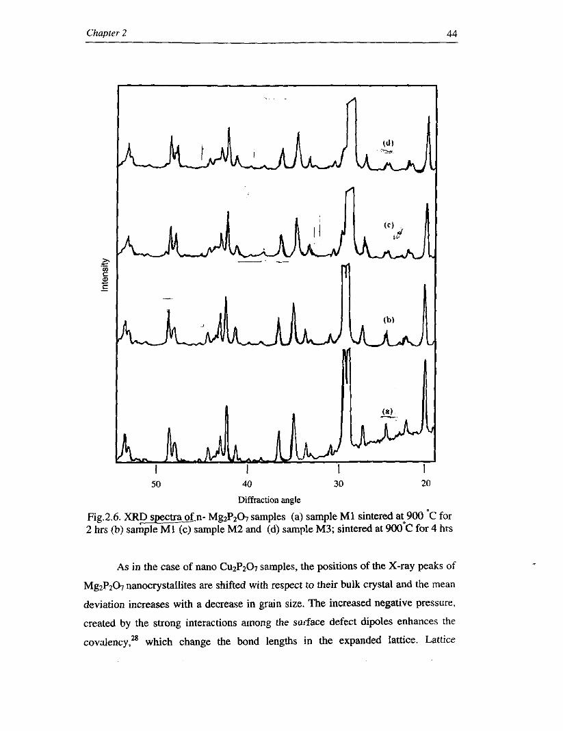
nm. The results are tabulated in table 2.7. The XRD patterns of the other two
samples of nanocrystalline magnesium pyrophosphate (MgzP207) prepared by
changing the reactant concentrations to 0.5 mol~ . ' and 0.1 mol~. ' (samples M2 &
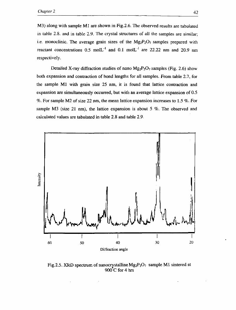
Chapter 2 42
M3) along with sample MI are shown in Fig.2.6. The observed results are tabulated
In table 2.8. and in table 2.9. The crystal structures of all the samples are similar;
i.e. monoclinic. The average grain sizes of the MgzPz07 samples prepared with
reactant concentrations 0.5 mol~. ' and 0.1 rnol~.' are 22.22 nm and 20.9 nm
respectively.
Detailed X-ray diffraction studies of nano MgzPz07 samples (Fig. 2.6) show
both expansion and contraction of bond lengths for all samples. From table 2.7, for
the sample M1 with grain size 25 nm, it is found that lattice contraction and
expansion are simultaneously occurred, but with an average lattice expansion of 0.5
%. For sample M2 of size 22 nm, the mean lattice expansion increases to 1.5 %. For
sample M3 (size 21 nm), the lattice expansion is about 5 %. The observed and
calculated values are tabulated in table 2.8 and table 2.9.
60 50 40 30
Diffraction angle
Fig.2.5. XKD spectrun: of nanoc~stallineMg2Pfi sample M1 sintered at 900 C for 4 hrs
Synthesis and Microstructural Characterization of Nanostructured Materials 43
Table 2.7. XRD pattern of nanocrystalline Mg2P207 sample M1
50 40 30
Diffraction angle
Fig.2.6. XRD spectra 0f.n- MgzPz07 samples (a) sample MI sintered at 900 'C for 2 hrs (b) sample M1 (c) sample M2 and (d) sample M3; sintered at 9 0 0 ~ ~ for 4 hrs
As in the case of nano Cu2P207 samples, the positions of the X-ray peaks of
Mg2P207 nanocrystallites are shifted with respect to their bulk crystal and the mean
deviation increases with a decrease in grain size. The increased negative pressure,
created by the strong interactions among the surface defect dipoles enhances the
covalency,28 which change the bond lengths in the expanded lattice. Lattice
Synthesis and Microstructural Characterization of Nanostructured Materials 45
!6:8i 1.541 1 :z 1 -1.248 1 1 3 3 1 1.522 -2.148 -5 2 3
62.3 1.489 1.476 -0.881 2 4 2
Table.2.8. XRI) pattern of nanocrystalline MgzPz07 sample M2
, I
20
2 1
22.6
23
25
27.5
29.6
31
33.6 - 35
36.6
Observed d values A
4.229
3.933
3.86:s
3.56
3.242
3.01'7
2.883
2.666
2.562
2.454
ICDD-PDF d values A
4.149
3.86
3.492
3.181
3.126
3.008
2.929
2.795
2.62
2.416
% of lattice contraction
-1.928
-1.891
-10.682
-11.914
-3.71 1
-0.299
1.571
4.615
2.214
-1.573
( h k 1 ) plane
0 2 0
1 1 1
0 2 1
-2 0 2
0 1 2
-30 1
2 2 0
-3 1 1
3 1 0
-2 2 2
Table.2.9. XRD pattern of nanocrystalline Mg2P207 sample M3
28
2 1
22.5
22.7
25
25.3
27.5
28.7
29.9
32.5
33.9
35.5
% of lattice contraction
- 1.928
-2.332
-12.142
-11.914
-12.572
-7.779
-6.145
-6.869 -- -5.115
-9.396
-8.223
( h k I ) plane
0 2 0
1 1 1
0 2 1
-2 0 2
0 1 2
-301
2 2 0
-3 1 1
3 1 0
-2 2 2
-3 2 1
Observed d values A
4.229
3.95
3.916
3.56
3.519
3.242
3.109
2.987
2.754
2.643
2.527
ICDD-PDF d values A
4.149
3.86
3.492
3.181
3.126
3.008
2.929
2.795
2.62
2.416
2.335

Synthesis and Microstructural Characterization of Nanostructured Materials 47
expansions have been measured in monodisperse Ce02 nanoparticles4' and in
BaTiO, single nanoparticles4' by electron diffraction. X-ray photoelectron
spectroscopy studies on Ce02 nanoparticles and on BaTi03 clusters show that the
origin of lattice expansion is the decrease of electrostatic force caused by valence
reduction of Ce ions and the increase in ionicity of Ti ions, respectively.
Thus the lattice parameter change of ionic nanoparticles with the increase in
ionicity would depend on the structure of the particles. In fact, a shift of the lattice
parameters with particle size variation may result from several different effects,30
such as changes of optical interband transitions, changes of electronic band
structure, changes of the effective mass of the conduction electrons etc.
Accordingly both contraction and expansion of the lattice parameters are possible in
the same crystal. It is evident that the relative importance of these effects for the
change of lattice parameters is different, depending on the experimental conditions
and materials.
The observation of the simultaneous expansion and contraction of the lattice
parameters in Mg2P207 nanocrystallites is in accordance with this argument. Due to
the small size of grains and the large surface-to-volume ratio of nanocrystals, the
atomic arrangements on the boundaries differ greatly from that of bulk crystals,
showing some extent of disorder. This disorder in crystal symmetry leads to the
broadening and shifting of many bands in the crystal The details of this observation
are given in the FTIR analysis of nano MgzP207 in section 3.2 (iii) of this thesis.
Since the resulting effect is bond length expansion, it may be assumed that
MgzP207 nanocrystallites contain ions with like charges4' in the atomic planes
parallel to the crystal axes. The negative intra-crystalline pressure thus produced
due to the electrostatic interaction between the elements of the lattice is responsible
for the expansion of lattice parameters. Bond length expansion may also be due to
the formation of capping layersz9 at the surface due to chemical impurities.
2.5 (iv) XRD Analysis of Nanocomposite Mg2P207- Fe3 (P04)2
The XRD pattern of nanocrystalline composite MgzP207 - Fe3 (PO& prepared
with Fe3(P04)2 content 5%. 10% and 15%, (samples S1, S2, & S3); all with

Chapter 2 48
Diffraction angle
Fig.2.7. X p spectra of nanocrystalline Mg~P207-Fe3 (PO& composite samples (a) sample S1 (b) sample S2 and (c) sample S3; sintered at 900 'C for 4 hrs
reactant concentrations 1.0 m o l ~ " are shown in Fig.2.7. The results are tabulated in
table 2.10, table 2.1 1 and table 2.12.
The observed 'd' values are compared with the standard ICDD-PDF values
of magnesium pyrophosphate Mg2P207 40 and also with iron phosphate Fe3(PO& 43
Using Scherrer formula the average grain sizes of the particles in the prepared
composites samples S1, S2 & S3 are estimated and are found to be 36.01 nm, 36.87

Synthesis and Microstrucrurul Characterization o f Nanostructured Materials 49
Table.2.10. XRD pattern of nanocrystalline MgzP2O-r-Fe3 (PO& sample S1
Table.2.11. XRD pattern of nanocrystalline Mg:P207-Fe3 (Pod2 sample S2
Synthesis and Microstructural Characterization of Nanostructured Materials 51
Observed d Values A d values A
Table.2.12. XRD pattern of nanocrystalline Mg~P207-Fe3 (PO& sample S3
Chapter 2 P
52
nm and 39.92 nm respectively. It is thus evident that as the weight percentage of
Fe3(P04)2 in the prepared nanocomposite MgzP~O~-Fe3(P04)2 increases, the grain ' / . . slze also increases.
A random displacement can be used to describe the substitution of
nano Fe3(P04)2 into the host nano Mg~P207. This allows the use of an empirical law
that relates the statistical substitution of a guest lattice into the host lattice with the
experimentally observed degree of lattice change with increasing defect lattice
concentration. Statistical substitution into a lattice site is predicted to lead to a
lattice contraction for smaller ions and a lattice expansion for larger ions." The
shift in the lattice parameter in table 2.10 shows a lattice contraction of
approximately 0.1% as the concentration of the doped material increases to 5 %
(sample Sl). The observation of a linear contraction with increasing Fe,(P04)2
concentration suggests a displacement occurs at the lattice sites through a purely
statistical process."The mean lattice contraction in the XRD data increases to 0.15
% for sample S2 with increasing Fe3(P04)z content to 10 % , as given in table 2.1 1.
The lattice contraction for sample S3, with gust lattice concentration 15%, is about
0.5 % as observed from table 2.12.
For isolated particles, the lattice contraction plays an important role in the
size evolution due to their weak free path effect and strong surface stress.44 The
statistical substitution of a guest lattice into the host lattice will enhance the degree
of lattice change with the increase of defect ion concentration. It is to be noted that
the mean lattice contraction of each sample in the present investigation is extremely
small comparing with the values of their bulk counterparts. This may be due to the
fact that the lattice contraction produced in smaller ions is opposed by the lattice
expansion of larger ions as suggested by the random clisp!acement model." The
PDF analysis of nanocrystalline Mg2P20, with reactant concentrations 1.0 mo l~ . '
gives a mean lattice expansion as observed in section 2.5 (iii). Nanocrystalline
Fe3(P04)2 has a mean lattice c~ntract ion.~~ The combined effect of these two
natures is appearing as a resultant contraction when botk the samples are mixed to
form the present nanocomposite. Though both type of icr:s. hhvlng like charges and
unlike charges, are present in atomic planes parallel 1.2 the crysta! axes, there is a
Synthesis and Microstructural Characterization of Nanostructured Materials 53
net positive interaction energy due to the resultant intra-crystalline pressure, which
gives the net contraction of the lattice parameters of the present nanocomposite.
2.6. TEM Analysis of Nanocrystalline Materials
Transmission electron microscopy (TEM) is a unique method to get direct
imaging of nanoparticles, although some stmctural features can be raveled by X-ray
and neutron diffraction. TEM can provide a real space image on the atom
distribution in the nanocrystal and on its surface. It can also be used to get atomic
resolution lattice images and chemical information at a spatial resolution of 1 nm or
better, allowing direct identification of the chemistry of a single nanocrystal. With a
finely focused electron probe, the structural characteristics of a single nanoparticle
can be fully characterized.
Transmission electron microscopy allows imaging of individual crystallites
and the development of a statistical description of the size and shape of the particles
in a nanocrystalline sample.30 High magnification imaging with lattice contrast
allows the determination of individual crystallite morphology. It is found that the
morphology of the particles do not change with the change in the molar
concentration of the reactants during synthesis. The overall degree of aggregation is
better revealed by TEM image3', while the XRD image provides a better resolution
on determining the grain sizes. ' E M observations show the presence of
nanoparticles dispersed homogeneously within the matrix. In agreement with the
XRD spectra, dark field observations indicate the amorphous character of the
majority of the nanoparticles. It is possible to find particles that give rise to 3 ---- - - - . -
diffraction rings through which they could be identified. The selected area - . ~ - - -
.-
diffraction (SAD) show a series of rings ascribed to the main reflections
of the corresponding nanocrystalline phase.
Three types of contrast46 usually dominate images in TEM. First diffraction
contrast, which is produced due to distortion in the o~ientation of the crystal so that
the diffracted intensity of the incident electron beam is perturbed, leading to
contrast observed in bright field image. For nanocrystals, most of the grains are
Uefect-free in volume, while high densities of defects are localized at surfaces and 7
grain boundaries.Diffraction contrast is useful for capturing strain distribution in
Chapter 2 54
nanocrystals. Secondly, phase contrast, which is produced by the phase modulation
of the incident electron wave when transmits through the crystal potential. This type
of contrast is sensitive to the atom distribution in the specimen and it is the basis of
high resolution TEM. Finally, mass-thickness or atomic number produced contrast.
Atoms with different atomic numbers exhibit different powers of scattering and the
image contrast is sensitive to the average atomic number along the beam direction.
Nanocrystals exhibiting distinctly different properties from the bulk are mainly
due to their large portions of surface atoms and the size effect. The high-resolution
capability of TEM and the complimentary applications of the techniques make it a
powerful tool in identifying and quantifying the chemical and electronic structure of
nanomaterials. High-spatial resolution analysis is vitally important for solving many
of the practical problems of nanomaterials. Spectroscopy analysis of the solid-state
effects46 is a new direction of quantitative microscopy. The exploration of the fine
structure in TEM is likely to reveal rich information about bonding in crystals and
at interfaces. Also TEM is important for characterizing and measuring the
properties of individual nanostructures, from which the structure-property
relationship of nanostructures can be clearly registered.
At high temperatures many nanophase ceramic materials undergo phase
transitions4' as they convert from metastable crystal structures to the stable
thermodynamic phase. These transitions are of importance as their occurrence can
lead to large volume changes, resulting in cracks or defects in dense sintered
ceramics. In smaller particles the greater surface area can have drastic effects on the
thermodynamic stability as well as the kinetics of phase transformations. 48-50 If
such effects are known, it is possible to fabricate nanocrystalline samples, which
adopt the stable structure before sintering. The temperature behaviour of
nanocrystalline Alp04 is studied in this section using transmission electron
microscopy.
2.60) TEM analysis of nanocrystalline Alp04 \
The TEM studies of nanocrystalline Alp04 sintered from mom temperature
up to W C is described in this part. The transmission electron micrographs (TEM)

Synthesis and Microstructural Characterization of Nanostructured Materials 5 5
Fig.2.8.(b): TEM micrograph of nano AlP04 sample at 450 "C
Scale: 15mm= 1 pn
Fig.2.8.(a): SAD pattern of ' nano A P 0 4 sample at 450 OC
Fig.2.9.(a): SAD pattern of nano AlP04 sample at 750 "C
Fig.2.9.(b):TEM micrograph of nano AlP04 sample at 750 "C
Scale: 15mm=500 nm

Chapter 2 56
and their corresponding selected area diffraction (:SAD) patterns of nanocrystalline
Alp04 sintered at two different typical temperatures (450°C and 750°C) are shown
in Fig.2.8. and Fig.2.9. The TEM images were taken using the JOEL 200CX
electron microscope operated at an acceleration voltage of 160 kV. For TEM
studies, the sample powder was dispersed in methanol using an ultrasonic bath and
a drop of suspension was placed on a copper grid coated with holey carbon fi ~ r n . ' ~
The TEM bright-field images in Fig.2.8 and Fig.2.9 provide good reviews of the
sample surfaces. When this sample is subjected to heat treatments in a furnace it
clearly transform from the low temperature phospho-berlinite to high temperature
phospho-tridymite. In this case the berlinite phase is clearly seen at temperatures as
low as 450°C while at 750"C, it transforms to the stable phospho-tridymite phase.
Such data is in good agreement with numerous thermal studies of Alp04 nanophase
ceramics. These phase transitions are studied in detail using TG and DTA methods
in section 3.3(i) of this thesis. In addition, the peak widths are observed to decrease
sharply when the transition to tridymite occurs. 'This indicates that significant grain
growth occurs during the phase transformation. Above 450°C a number of changes
are observed. The most striking of these is the increased fluctuation in the shape of
the particles, significantly during sintering. Strong selected area electron diffraction
is observed from these nanocrystals, which appear bright in dark field illumination
indicating that a large fraction of the material is crystalline. The micrographs show
an aggregation appeared in part of the particles. This observation is also consistent --- with the fact that average nanoparticle sizes of the present sample increase between A
temperatures 400°C and 900°C with final sizes as large as 50 nm. In addition, the
sample shows new rings and spots in selected area electron diffraction patterns at
750°C, matching with other observations of this crystalline product. The
diffractogram of high-resolution image of the heated nanocrystal shows spots that I
correspond to the d-spacings of the crystal. Extensive examinations show that the
common crystallite defects, stacking faults, twin planes etc. are minimum in the
present nanocrystalline sample.

Synthesis and Microstructural Characterization of Nanostructured Materials 57
2.7. Conclusion
Three different nanocrystalline metal phosphates; namely, aluminium
phosphate (AlP04). copper pyrophosphate (CuzPz07) and magnesium
pyrophosphate (Mg2PZ07), in three different reactant concentrations (1.0 molL ',0.5
m o l ~ . ' & 0.1 mol~. ' ) were synthesized, by following a versatile, efficient and
simple chemical route. The nanocrystalline composite Mg2P207 - Fe3 (P04)2 was
also prepared in a similar manner by changing the content of iron phosphate in three
different weight percent. The grain size and crystal structure of all the prepared
samples were analyzed, as a function of sintering temperature and time, using X-ray
diffraction and transmission electron microscopy techniques. The XRD and TEM
observations are shown in figures. The results are tabulated. It is observed that as
the reactant concentration decreases, the size of the grains also decreases. The mean
crystallite sizes of the Alp04 samples were estimated to be16 nm, 13.5 nm and 12
nm, for reactant concentrations 1.0 m o l ~ ~ ' , 0.5 m o l ~ . ' & 0.1 m o l ~ . ' respectively.
All the samples are of cubic structure. The average grain sizes of the Cu2P207
samples prepared with reactant concentrations 1.0 mol~. ' , 0.5 m o l ~ ~ ' and 0.1 molL-
' are 34.5 nm, 32 nm and 27 nm respectively. The crystal structure of all the
samples in this case was found to be monoclinic. For the Mg2P207 samples, the
average grain sizes were estimated to be 25nm, 22 nm and 21 nm respectively. In
the case of the nanocomposite, the grain size was found to increase as the iron
phosphate content in the composite increases. The average grain sizes of the
different composite samples Mg~P207 - Fe3(P04)2 with different Fe3 (PO& weight
percent (= 5%, 10% and 15%) prepared with reactant concentrationl.0 mol~ . ' were
found to be 36 nm , 37 nm and 40 nm respectively. The well-defined peaks in the
XRD spectrum of each sample clearly indicate the crystalline nature at higher
sintering conditions.
The quantitative determination of nanoparticle crystallinity and disorder,
using a PDF-based method is adopted in this work. It is found that the best % description of nanoparticle structure includes bond length contraction and
expansion, random disorder, and a type of disorder characterized by correlated
atomic displacements. The PDF analysis of nano AIP04 samples indicates more and
Chapter 2 58
more bond length compression as particle size decreases, which is characteristic of
ionic crystals. In covalent crystals, unit cell volume increases as particle size
decreases, which is accompanied by an increase in the lattice parameters.
Nanoclystalline Cu2P207 is showing an exactly similar character. The observation
of the simultaneous expansion and contraction of the lattice parameters in Mg2P207
nanocrystallites is due to several different effects, such as changes of optical
interband transitions, changes of electronic band structure, changes of the effective
mass of the conduction electrons etc. which are the features of ionic crystals. The
changes in the lattice parameters of MgZP207-Fe3(P04)2 nanocomposite is explained
using a random displacement model. From the PDF analysis, it is observed that the
sample has a mean lattice contraction.
The TEM and SAD patterns are used to study the phase changes with
temperature of n- AlP04 samples. The TEM bright-field images show that the
berlinite phase at 450°C, transforms to the stable phospho-tridymite phase at 750°C,
consistent with the TG-DTA analysis. The rings and spots in selected area electron
diffraction patterns indicate that a large fraction of the material is crystalline.
References
1. Francisco E Fujita, Physics of new materials, Springer series in materials
Science, 27.4, Springer-Verlag Berlin Heidelberg (1994).
2. Glenn A. Waychunas, Structure, Aggregation and Characterization of
Nanoparticles, 4, Cambridge University Press, Oxford, UK (1993).
3. M Wu, W Gu, W Li, X Zhu, F Wang & S Zhao, Chem. Phys. Lett. 224: 557
(1998).
4. M Abdul Khadar and Binny Thomas. Phys. Stat. Sol. (a) 150, 755 (1995)
5. S Sankaranarayanan Potty and M Abdul Khadar. Bull. Muter. Sci. 23 (9, 361
(2o'x))
6. Harisingh Nalwa, Nanostructured Materials and Nanotechnology, 1(1), 2
Academic Press, USA (2000).

Synthesis and Microstructura[ Characterization of Nanostructured Materials 59
7. R.W.Siegel, S. Ramasamy, H.Hahn, Li Zongquan, and Lu Ting, J. Mater. Res.
3,6, (1988)
8. Gan-Moog Chow, Proceedings of the NATO Advanced Study Institute on
Nanostructured Materials: Science &Technology, S t . Petersburg, Russia,
(1997)
9. D JAnderton and F R Sale, Powder Metall.1, 8, (1979)
10. M P Pechini, US Patent, 3, 330,697, (1967).
11. P Pramanik, Bull. Mater. Sci., 18,819, (1996).
12. Ruitao Wu, Yu Wei, and yanfeng Zhang, Mater. Res. Bull., 34, 14/15, 2131,
(2000)
13. P Pramanik, Bull Mater Sci, 22(3), 335, (1999).
14. R. Bininger, H. Gleiter, H.P.Klein, P. Marquardt, Phys.Lett.,l02A, 365, (1984)
15. G W Nieman, J R Weertman & R W Siegel, scripta Met et Mater, 23(12),
2013, (1989)
16. G E Fougere, J R Weertman, R W Siegel & S Kim, scripta Met et Mater,
26(12), 1879, (1992)
17. X Y Qin, X J Wu & L D Zhang, Nanostructered Materials, 5 (I), lOl(1995)
18. J Lee, J H Hwang, J J Mashek, T 0 Mason, A E Miller and R W Siegel, Mater.
Res. 10,2295, (1995)
19. W Puin and P Heitjans, Nanostruct. Mater. 6,885 (1995)
20. Joshy Jose and M Abdul Khadar, Nanostr. Mater. 2(8), 1091 (1999)
21. Gordon Burely, J Phys. Chem, 68, 11 11, (1964).
22. A J Manjumdar and Rustom Roy, J Phys. Chem., 63,1858, (1959)
23. M.C.Chen, S.D.Tsai, M.R.Chen, S.Y.C)u, W.H.Li and K.C.Lee, Phys. Rev. B,
51,7,4507, (1995).
24. D.H.Ping, D.X.Li, andH.Q.Ye, J. Mater. Sci. Lett., 14, 1536, (1995).
Chapter 2 60
25. Harold P Hug and Leroy E Alexander, X-ray Dtffraction Procedures, John
Wiley & Sons, (1974).
26. Pushan Ayyub, Physics Education 14,4 (1998)
27. J E Lennard-Jones, Z. Crystallography 75,215 (1930)
28. M Ya Garnamik, Physica Status Solidi(b) 161,457 (1990)
29. Chang Q. Sun, S. Li, and B. K. Tay, Appl. Phys. Lett. 82,20 (2003)
30. Caria Cannas, Mariano Casu, Adolfo Lai, Anna Musinu and Giorgio Piccaluga,
J. Muter. Chem., 9, 1765, (1999)
31. W. Cai, H. Hofmeister and M. Dubiel, Eur. Phys. J . D 13, 245 (2001)
32. M.C.Chen, S.D.Tsai, M.R.Chen, S.Y.Ou, W.H.Li and K.C.Lee.., Phys. Rev. B,
51, 7,4507, (1995).
33. International Center for Diffraction Data - Powder Diffraction Files, No.31-28
34. W.H.Qi, M.P.Wang, G.Y.Xu, Z .Li and J.Y.Chen, China-BJ forum on
nanosized Technology, Beijing, P.R. China, (2002).
35. A.Puzder, A.J.Williamson, F.A.Reboredo and G.Galli, Phys.Rev.Lett.91,
157405 (2003)
36. H.Zhang, B.Gilbert, F.Huang and J.F.Ban .eld, Nature 424,1025 (2003).
37. International Center for Diffraction Data -Powder Diffraction Files, No.44- 182.
38. S B Qadri, J P Yang, E F Skelton, and B R Ratna, Appl. Phys. Lett. 70(8), 1020
(1997)
39. Guangshe Li, Juliana Boerio-Goates, Brian F. Woodfield, and Liping Li, Appl.
Phys. Lett. 85 ( 1 1). 2059 (2004)
40. International Center for Diffraction Data -Powder Diffraction Files, No.32-626.
41. P Ayyub, V R Palkar, S Chattopadhyay and M S Multani, Phys. Rcv. HS1,
6135 (1995).
42. 5 Tsunekawa, X Y Qin, D H Ping, and Z Li, Phys. I&. Lrtr. 85, .M40 (20i)O)
43. International Center for Diffraction Data -Powder Diffrdction Fi!es, No.27-250. '
Synthesis and Microstructural Characterization qfNanostructured Materials 6 1
44. Orlando E. Raola and Geoffrey F. Strouse, Nano Leu., 2, 12 (2002)
45. A Q Jiang, G H Li, and L D Zhang, J. Appl. Phys. 83(9), 4878 (1998)
46. J M Cowley, "Dzffraction Physics" 31d revised ed., New York, Elsvier Science
B. V. (1995)
47. M Barsourn, Fundamentals of Ceramics., Mc-Graw Will, New York (1997).
48. L H Edelson and A M Glaeser, J . Am. Ceram. Soc. 71(4), 225 (1988).
7 49. K P Kumar, K Keizer and A J Burggraaf J. Mater. Sci. Lett.59 (1994). . 7 o-' ,
50. B L Bischoff and M A Anderson, Chem Mater. 7, 1772 (1995).