synthesis and surface engineering of complex ... · pdf filesynthesis and surface engineering...
TRANSCRIPT

DOI: 10.1002/adma.200700079
Synthesis and Surface Engineeringof Complex Nanostructures by Atomic LayerDeposition**
By Mato Knez,* Kornelius Nielsch, and Lauri Niinistö
1. Introduction to ALD and Its Applications inNanotechnology
Atomic layer deposition (ALD), originally called Atomiclayer epitaxy (ALE), was developed in the 1970s by Suntolaand Antson to meet the needs of producing high-quality,large-area flat panel displays based on thin film electrolumi-
nescence (TFEL).[1] ALD is based on successive, surface-con-trolled reactions from the gas phase to produce thin films andoverlayers in the nanometer range with perfect conformalityand process controllability. The principle of ALD is schemati-cally shown in Figure 1 where the thin film growth cycle for abinary compound (TiO2) from gaseous precursors (TiCl4 andH2O) is presented as an example.
The TFEL flat panel displays, produced on an industrialscale since 1983, consist of a stack of thin film layers on a glasssubstrate through which the display is viewed. In the simplestcase (a monochromatic yellow-emitting display) the TFELstructure contains a semiconducting light-emitting core (Mn-doped ZnS) surrounded by dielectric layers (Al-Ti-oxide,ATO). In addition, a transparent front electrode (In-Sn-oxide,ITO) and a back electrode (Al) are needed together with pas-sivation and ion barrier layers. As the layer thicknesses aretypically in the range of 150–500 nm each, the total thicknessof the structure exceeds 1500 nm. The multi- and full colordisplays have even more complex structures and often involveco-doping. Nevertheless all layers, except for the Al back elec-trode, can be deposited and doped by ALD.[2]
The processing of TFEL displays by ALD illustrates theadvantages of this technique compared to CVD and PLD, forinstance. ALD can provide a simple and accurate thicknesscontrol as it can be controlled with every cycle. Furthermore,ALD offers facile doping, large area uniformity and thus
REV
IEW
Adv. Mater. 2007, 19, 3425–3438 © 2007 WILEY-VCH Verlag GmbH & Co. KGaA, Weinheim 3425
–[*] Dr. M. Knez, Prof. K. Nielsch
Max Planck Institute of Microstructure PhysicsWeinberg 2, 06120 Halle (Germany)E-mail: [email protected]. K. NielschInstitute of Applied Physics, University of HamburgJungiusstr. 11, 20335 Hamburg (Germany)Prof. L. NiinistöLaboratory of Inorganic and Analytical ChemistryHelsinki University of TechnologyP.O. Box 6100, 02015 Helsinki (Finland)
[**] The authors of this article want to thank the authors of the reprintedimages for their kind assistance in providing the original imagesand Prof. U. Gösele for his valuable comments. L.N. gratefullyacknowledges the financial support by the Max-Planck-Institute ofMicrostructure Physics during his stay in Halle. M.K. and K.N.gratefully acknowledge the financial support by the German FederalMinistry of Education and Research (BMBF) via contract numberFKZ 03X5507 and FKZ 03N8701, respectively.
Atomic layer deposition (ALD) has recently become the method ofchoice for the semiconductor industry to conformally process extremelythin insulating layers (high-k oxides) onto large-area silicon substrates.ALD is also a key technology for the surface modification of complex nanostructured materi-als. After briefly introducing ALD, this Review will focus on the various aspects of nanomateri-als and their processing by ALD, including nanopores, nanowires and -tubes, nanopatterningand nanolaminates as well as low-temperature ALD for organic nanostructures and biomateri-als. Finally, selected examples will be given of device applications, illustrating recent innovativeapproaches of how ALD can be used in nanotechnology.
straightforward scale-up. The films exhibit excellent conform-ality and are dense and pinhole-free. The reactant flux doesnot need to be controlled as the process is surface-controlled.
In addition to the industrial processing of TFEL displays,ALD has been successfully applied to the depositing of oxidematerials including high-k insulators[3,4] and other ultrathinmetal-oxide films for device applications.[5] A broad overviewof successfully deposited materials and the deposition condi-tions have been given by Puurunen[6] and Kim.[7] Amongthem the currently mostly investigated materials are, e.g.,
HfO2 for electronic applications, but also other metal oxidesand nitrides like ZnO, TiO2, WNx, or Al2O3 because of theirelectrical or mechanical properties. Apart from those materi-als a considerable interest can be seen for deposition process-es of metals for applications as electrode materials. Here,several groups developed processes for the deposition of Pt,Ru, or Ta.[6]
Besides these applications, the unique potential of ALD forprocessing nanostructured materials, in general, has been ap-preciated.[8] The most important large-scale industrial applica-
REV
IEW
M. Knez et al./Complex Nanostructures by Atomic Layer Deposition
3426 www.advmat.de © 2007 WILEY-VCH Verlag GmbH & Co. KGaA, Weinheim Adv. Mater. 2007, 19, 3425–3438
Dr. Mato Knez was born in 1971 in Augsburg, Germany. He studied chemistry at the Universityof Ulm (1993–1998) and did his diploma thesis on the synthesis, characterization and theoreticalmodeling of carbocations. During his doctoral research at the Max-Planck-Institute of Solid StateResearch in Stuttgart (2000–2003) he investigated the application of plant viruses as templates forthe synthesis for novel nanostructures. Subsequently he received his doctoral degree from theUniversity of Ulm. From December 2003 he worked as a post-doctoral researcher at the Max-Planck-Institute of Microstructure Physics in Halle on the application of Atomic Layer Deposi-tion in Nanotechnology. Since November 2006 he is leader of a nanotechnology research groupfunded by the German Federal Ministry of Education and Research (BMBF) on FunctionalNanostructures by Atomic Layer Deposition at the Max-Planck-Institute in Halle.
Prof. Kornelius Nielsch was born in Hamburg, Germany in 1973. He studied physics at the Mer-cator University in Duisburg (1993–97) and conducted his diploma work on the aerosol synthesisof semiconductor nanoparticles at the University of Lund, Sweden. Subsequently, his doctoralstudies on template-based ferromagnetic nanowire arrays were carried out at the Max-Planck-In-stitute of Microstructure Physics in Halle, Germany. In 2002 he received his doctoral degree withdistinction from the Martin-Luther-University Halle–Wittenberg. From October 2002 he workedas a postdoctoral associate at the Massachusetts Institute of Technology, Cambridge, USA. SinceOctober 2003 he is leader of a nanotechnology research group funded by the German FederalMinistry of Education and Research (BMBF) on Multifunctional Nanowires and Nanotubes atthe Max-Planck-Institute in Halle. He has co-authored more than 65 refereed journal publica-tions and 3 patents. In 2006 the University of Hamburg has appointed him as a W2 Professor(Associate Professor) for Experimental Physics. Also in 2006, the State of Saxony-Anhaltawarded him the State Research Prize for Basic Research. Since May 2007 he is working as pro-fessor at the Institute of Applied Physics in Hamburg.
Prof. Lauri Niinistö was born in Helsinki, Finland, in 1941. He received his M.Sc. and D.Techn.degrees from Helsinki University of Technology in 1968 and 1973, respectively. His doctoralresearch on the synthesis and crystal structures of metal sulfates and sulfites was partly conductedat the University of Stockholm in 1971–1972. Since 1977 he has been Professor of InorganicChemistry at TKK but also worked in France, USA, Austria, and Hungary. His current researchis focused on the preparation and characterization of thin films for optoelectronic and electronicdevices. He is the author or co-author of more than 400 original publications and reviews. Hehas received several international honors, among them the Cannizzaro gold medal of the ItalianChemical Society (1996), the FECS award (2000), and honorary doctorates from Tallinn (1990)and Budapest (2002).

tion, however, has recently emerged in the semiconductorindustry where ALD has been considered as the technique todeposit very thin, highly insulating (high-k) oxides to serve asgate dielectrics in MOSFETs and as dielectrics in the trenchcapacitor structures. As the trench aspect ratio is expected toincrease up to 80:1 by the year 2007, ALD is probably theonly viable technique for such depositions.[9]
Recently, ALD has attracted the attention of researchers innanotechnology. The precise control of the deposited layerthickness allows for new strategies in the modification ofchemical and physical properties of nanoscaled materials andsynthesis routes to novel nanostructures. This review will givean overview of the recently evolved work on the applicationsof ALD in nanotechnology. The focus is on areas in which thespecial features of ALD can be exploited, namely the modifi-cation or functionalization of existing organic and inorganicnanostructures, the construction of optical devices, like pho-tonic crystals or solar cells, or nanostructures for future elec-tronic devices.
2. Tuning of Nanopores and Porous Materials
Porous materials, particularly with one-dimensional high as-pect ratio pores, are of major interest as templates for the syn-thesis of nanowires and nanotubes. The unique potential ofALD for depositions into nanopores and trenches has beenrealized since the demonstration of SnO2 coating of poroussilicon with an aspect ratio (AR) of 1:140.[10] Gordon et al.[11]
presented a simple kinetic model for step coverage by ALDand also experimentally tested it for the deposition of HfO2 innarrow holes with AR = 43. However, the pore size of macro-porous silicon is comparatively large. The potential of ALDto coat narrow pores becomes obvious if, e.g., mesoporous sili-con is used as template. In a recent work, various metal oxidesfrom W, V, Mo, and Ti were deposited on such materials.[12]
Highly uniform nanoporous anodic alumina (AA) can beused as a nanoscale template to test the ALD coating both inpractice and theory.[13] ZnO deposition into ultrahigh-aspect-ratio (AR = 5000) nanopores of AA was experimentally dem-onstrated and modeled with Monte Carlo simulations whichpredicted that the diffusion-limited coating process would be-come reaction-limited. Recently, the same group depositedZnO also on ultra-low density nanoporous silica aerogelmonoliths with an effective AR around 100 000 (defined asthe ratio of the monolith thickness to average pore size).[14]
Even the deposition of metals (W and Ru) on highly porousaerogels to obtain a very high metal surface area was success-fully performed.[15,16]
Dense, aligned and uniform arrays of TiO2 nanotubes werefabricated by ALD with the TiCl4/H2O process on nanopo-rous Al203 templates on a silicon substrate (Fig. 2).[17] The alu-mina template was then chemically removed to reveal nano-tubes with perfectly controllable tube diameter, spacing andwall thickness. In a similar manner ZnO-nanowires were pro-duced by ALD deposition onto a porous alumina template[18]
or the pore sizes were reduced by ALD in order to control thethickness of nanowires produced by successive electrochemi-cal deposition.[19] Very recently the group of M. Leskelä dem-onstrated the photocatalytic properties of such TiO2-mem-branes.[20]
REV
IEWM. Knez et al./Complex Nanostructures by Atomic Layer Deposition
Adv. Mater. 2007, 19, 3425–3438 © 2007 WILEY-VCH Verlag GmbH & Co. KGaA, Weinheim www.advmat.de 3427
a) Precursor 1
b) Purge
c) Precursor 2
d) PurgeCycle
Figure 1. Schematic of an ALD process. The gas flow is indicated withthe white arrow. One ALD cycle consists of four separate steps. In stepa) the substrate is exposed to precursor molecules (precursor 1) whichadsorb ideally as a monolayer on the surface. In step b) the excess of pre-cursor 1 in the gas phase is removed by inert gas purging. In step c) thesubstrate is exposed to precursor 2 which reacts with the adsorbed pre-cursor 1 to form a layer of the desired material. In step d) the excess ofprecursor 2 and the reaction by-products are removed by purging. Thiscycle is repeated (yellow arrow) until the desired thickness of the depositis obtained.
1 2
34
ALD
Mechanically
polish
Remove
template
Figure 2. Schematic of the process to create titania nanotube arrays onsubstrates. 1) Nanoporous-alumina template on a substrate created byanodization of Al film. 2) TiO2 deposited onto the surface of the templateby ALD. 3) Top layer of TiO2 on alumina removed by gentle mechanicalpolish. 4) Alumina template chemically etched away to reveal array of ti-tania nanotubes on the substrate. Reproduced with permission from[17].

Other oxide materials fabricated as nanotubes by ALD in-clude TiO2 and ZrO2.[21] In this work a commercially availablepolycarbonate (PC) filter was used as template (AR = 60:1) tobe chemically etched away after the ALD deposition at140 °C. The free-standing nanotubes with ca. 30–200 nmdiameters could be fabricated in a one-step process becausemicrocontact printed OTS-SAMs prevented deposition ontoboth sides of the PC template. These authors also exploitedthe gas sensing properties of these metal oxide nanotubes.Nb2O5 nanotubes have been synthesized in porous anodic alu-mina templates by an ALD process based on NbI5 and oxygenby a Swedish group.[22] Niobium oxide (Nb2O5) exhibits bothelectrochromism and catalytic activities.
Furthermore, the honeycomb-like alumina pore structureshave been also coated by metallic materials. Most processesfor transition metals, like, e.g., Cu, Ni, and Co, based on thereactions of H2 and organometallic precursors proceed ratherslowly (0.03–0.2 Å/cycle).[23] Johansson et al.[24] have em-ployed a three-step ALD process. First, the nanopores areexposed to the copper chloride (CuCl). After the removal ofthe excess precursor molecules, the chemisorbed moleculeson the pore walls are exposed to water and form Cu2O. In thefinal step of the ALD cycle the sub-monolayer of metal oxideis transformed into a pure metallic layer by a hydrogen pulse.The three-step process yields a granular and discontinuousmetallic film on the pore walls. This three-step ALD processwas originally introduced by Utriainen et al.[25] who processedNi films by first depositing NiO and then reducing it by H2. Amore direct approach is also possible when the metal beta-di-ketonate precursor M(acac)2 (M = Ni, Cu, Pt) is chemisorbedonto the substrate and then reduced by H2 in the same ALDcycle.[25] Daub et al.[26] applied a very similar three-step ALDprocess based on NiCp2 (Nickelocene) and CoCp2 (Cobalto-cene) for the synthesis of nickel and cobalt nanotubes inporous alumina membranes and obtained quite granular met-al films. Alternatively, they tried the deposition of nickel andcobalt oxide by using the same precursors and ozone pulses.After the ALD process, the transition metal oxide tubes werereduced in hydrogen at elevated temperatures. The resultingferromagnetic nanotubes exhibited significantly improvedmagnetic properties, a preferential magnetization directionalong the tube axis, a very fine granular crystal structure and alow degree of surface roughness. The reduction of atomiclayer deposited metal oxides or nitrides seems to be a verypromising approach for the formation of continuous transitionmetal films on complex surfaces. This process has also beensuccessfully applied on atomic layer deposited copper nitridefilms in high aspect ration silicon trenches by the Gordongroup.[27]
ALD can also be used to fine-tune the surface propertiesand diameters of nanopores to achieve functional nanoporedetectors.[28] Using 5 cycles of the well-established aluminaALD process from TMA and water, a 2 nm diameter ion-beam sculpted nanopore could be reproducibly adjusted downto 1 nm diameter, with an error of only ± 0.12 nm.
3. VLS Growth of Semiconductor Nanowires
The synthesis of semiconductor nanowires NWs is currentlyvery intensively studied[29] by means of pulsed laser deposi-tion (PLD), molecular beam epitaxy (MBE) and chemical va-por deposition (CVD). Most semiconducting materials, e.g.,Si, Ge, ZnO, and GaAs have been realized by this approachand published in several hundred papers each year. Thegrowth of multilayer nanowires with atomic resolution at theinterfaces is challenging and for certain material systems, e.g.,InP/InAs, high-resolution multilayer nanowires have beensuccessfully synthesized.[30] In combination with ALD a bettercontrol of VLS growth for binary semiconductor nanowiresfor a broader range of materials could be provided.
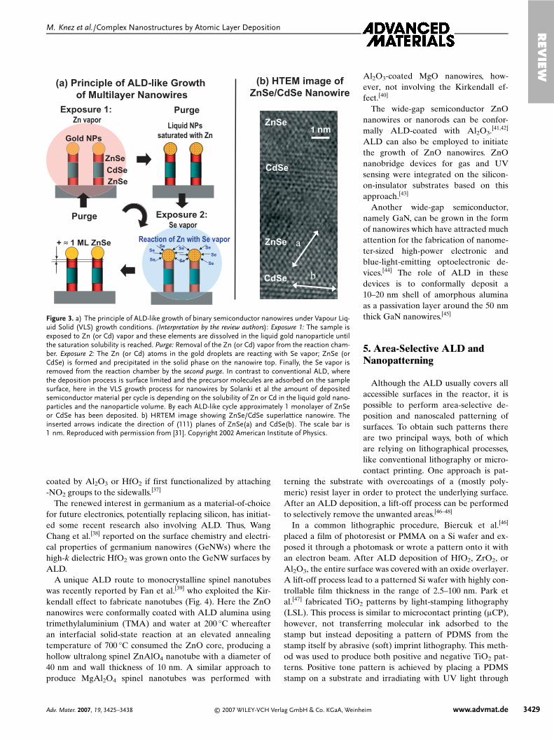
The processing of both II-VI and III-V semiconductornanowires by ALD has been successfully demonstrated. TheVapor–Liquid–Solid (VLS) growth has been used to initiateALD of single crystalline nanowires consisting of alternatinglayers of ZnSe and CdSe which form a superlattice (Fig. 3)[31]
while a pulsed MOCVD process has been used to depositGaN.[32] Because of the strict separation of the precursorpulses (trimethylgallium and ammonia) the latter process byits nature appears to represent essentially ALD.
Another recent example of employing ALD for the growthof nanowires is the formation of KCl NWs by a rather unusualtwo-step process where at first tantalum oxide is formedinside microchannel glass by a conventional ALD reactionfrom TaCl5 and H2O. In the next stage, the hydrogen chloridereleased in the ALD reaction etches K2O from the glass sub-strate whereupon forming KCl and water. The final phase inthis process chain involves the nucleation of KCl on themicrochannel walls to form KCl nanowires. The aspect ratioof the nanowires is about 10 to 100. They span the entirelength of the 5 lm channels and the NW diameter rangesfrom 50 to 700 nm.[33]
There should not be any fundamental reason that the ALDgrowth of semiconductor NWs should be limited to these fewexamples. It can most probably be extended to other binarysemiconductors. The research activity in this area is likely toincrease rapidly in the very near future.
4. Conformal Coating of CNTs and SemiconductorNanowires
The surface-controlled nature of ALD can be exploited toan extreme when nanotubes and nanowires are coated toachieve the desired materials properties for functional deviceapplications. Thus, carbon nanotubes (CNTs) possessing awell defined molecular and nanoscale hollow tubular struc-ture can be functionalized as such by ALD coatings[34,35] orused as templates for nanotubes of various inorganic oxidessuch as ruthenium oxide.[36] Suspended single-walled carbonnanotubes are known to be chemically inert to ALD precur-sor molecules but nevertheless they can be conformally ALD-
REV
IEW
M. Knez et al./Complex Nanostructures by Atomic Layer Deposition
3428 www.advmat.de © 2007 WILEY-VCH Verlag GmbH & Co. KGaA, Weinheim Adv. Mater. 2007, 19, 3425–3438
coated by Al2O3 or HfO2 if first functionalized by attaching-NO2 groups to the sidewalls.[37]
The renewed interest in germanium as a material-of-choicefor future electronics, potentially replacing silicon, has initiat-ed some recent research also involving ALD. Thus, WangChang et al.[38] reported on the surface chemistry and electri-cal properties of germanium nanowires (GeNWs) where thehigh-k dielectric HfO2 was grown onto the GeNW surfaces byALD.
A unique ALD route to monocrystalline spinel nanotubeswas recently reported by Fan et al.[39] who exploited the Kir-kendall effect to fabricate nanotubes (Fig. 4). Here the ZnOnanowires were conformally coated with ALD alumina usingtrimethylaluminium (TMA) and water at 200 °C whereafteran interfacial solid-state reaction at an elevated annealingtemperature of 700 °C consumed the ZnO core, producing ahollow ultralong spinel ZnAlO4 nanotube with a diameter of40 nm and wall thickness of 10 nm. A similar approach toproduce MgAl2O4 spinel nanotubes was performed with
Al2O3-coated MgO nanowires, how-ever, not involving the Kirkendall ef-fect.[40]
The wide-gap semiconductor ZnOnanowires or nanorods can be confor-mally ALD-coated with Al2O3.[41,42]
ALD can also be employed to initiatethe growth of ZnO nanowires. ZnOnanobridge devices for gas and UVsensing were integrated on the silicon-on-insulator substrates based on thisapproach.[43]
Another wide-gap semiconductor,namely GaN, can be grown in the formof nanowires which have attracted muchattention for the fabrication of nanome-ter-sized high-power electronic andblue-light-emitting optoelectronic de-vices.[44] The role of ALD in thesedevices is to conformally deposit a10–20 nm shell of amorphous aluminaas a passivation layer around the 50 nmthick GaN nanowires.[45]
5. Area-Selective ALD andNanopatterning
Although the ALD usually covers allaccessible surfaces in the reactor, it ispossible to perform area-selective de-position and nanoscaled patterning ofsurfaces. To obtain such patterns thereare two principal ways, both of whichare relying on lithographical processes,like conventional lithography or micro-contact printing. One approach is pat-
terning the substrate with overcoatings of a (mostly poly-meric) resist layer in order to protect the underlying surface.After an ALD deposition, a lift-off process can be performedto selectively remove the unwanted areas.[46–48]
In a common lithographic procedure, Biercuk et al.[46]
placed a film of photoresist or PMMA on a Si wafer and ex-posed it through a photomask or wrote a pattern onto it withan electron beam. After ALD deposition of HfO2, ZrO2, orAl2O3, the entire surface was covered with an oxide overlayer.A lift-off process lead to a patterned Si wafer with highly con-trollable film thickness in the range of 2.5–100 nm. Park etal.[47] fabricated TiO2 patterns by light-stamping lithography(LSL). This process is similar to microcontact printing (lCP),however, not transferring molecular ink adsorbed to thestamp but instead depositing a pattern of PDMS from thestamp itself by abrasive (soft) imprint lithography. This meth-od was used to produce both positive and negative TiO2 pat-terns. Positive tone pattern is achieved by placing a PDMSstamp on a substrate and irradiating with UV light through
REV
IEWM. Knez et al./Complex Nanostructures by Atomic Layer Deposition
Adv. Mater. 2007, 19, 3425–3438 © 2007 WILEY-VCH Verlag GmbH & Co. KGaA, Weinheim www.advmat.de 3429
a
b
ZnSe
CdSe
ZnSe
Gold NPs
Exposure 1: Zn vapor
Liquid NPs
saturated with Zn
Purge
Exposure 2: Se vapor
Purge
Reaction of Zn with Se vapor+ ≈ 1 ML ZnSe
CdSe
CdSe
ZnSe
ZnSe
1 nm
(b) HTEM image of
ZnSe/CdSe Nanowire(a) Principle of ALD-like Growth
of Multilayer Nanowires
Se
SeSe
SeSe
Se
Se Se
Figure 3. a) The principle of ALD-like growth of binary semiconductor nanowires under Vapour Liq-uid Solid (VLS) growth conditions. (Interpretation by the review authors): Exposure 1: The sample isexposed to Zn (or Cd) vapor and these elements are dissolved in the liquid gold nanoparticle untilthe saturation solubility is reached. Purge: Removal of the Zn (or Cd) vapor from the reaction cham-ber. Exposure 2: The Zn (or Cd) atoms in the gold droplets are reacting with Se vapor; ZnSe (orCdSe) is formed and precipitated in the solid phase on the nanowire top. Finally, the Se vapor isremoved from the reaction chamber by the second purge. In contrast to conventional ALD, wherethe deposition process is surface limited and the precursor molecules are adsorbed on the samplesurface, here in the VLS growth process for nanowires by Solanki et al the amount of depositedsemiconductor material per cycle is depending on the solubility of Zn or Cd in the liquid gold nano-particles and the nanoparticle volume. By each ALD-like cycle approximately 1 monolayer of ZnSeor CdSe has been deposited. b) HRTEM image showing ZnSe/CdSe superlattice nanowire. Theinserted arrows indicate the direction of (111) planes of ZnSe(a) and CdSe(b). The scale bar is1 nm. Reproduced with permission from [31]. Copyright 2002 American Institute of Physics.

the polymeric master. The PDMS in the contact area isbonded to the substrate and after mechanical removal of themaster, PDMS remains in the initial contact areas. For thenegative tone pattern, a layer of TiO2 is deposited by ALD onthe substrate. After removal of the PDMS master and chemi-cal etching, a TiO2 pattern remains on the substrate (Fig. 5).Alternatively, the substrate is covered with a TiO2-layer andafterwards treated by LSL, which then, after the lift-off pro-cess, leads to a positive pattern. Although this method wasdemonstrated for TiO2 only, it is expected that it will work ina similar manner for a number of other materials, too.
A different patterning approach via ALD is the passivationof surface areas by immobilizing molecules which hinder theALD precursor molecules to attach.[48–52] In those cases, a sep-arate lift-off process is not required. The driving force for theinhibition of ALD deposition in selected areas is the repulsiveforce between the deposited monolayers of molecules and theprecursor molecules approaching from the gas phase. In mostcases, the selectivity arises from polar and non-polar mole-cules building a pattern on the substrate. A commonly usedtechnique to produce such a molecular pattern is soft-imprint-lithography. For this purpose, a patterned polymer master wasinked with molecules prior to the contact with the substrate.
The molecules adsorb locally on the substrate and thus changethe chemical environment. If both the monolayer and theALD precursor molecules are polar, no ALD deposition inthose areas is expected. The work of Seo et al.[48] shows pat-terning of gold with non-polar thiol-monolayers and succes-sive immobilization of a polar self-assembled thiol monolayerin the remaining area. An ALD deposition of TiO2 took selec-tively place in the area of polar molecules. A similar approachwas performed by Park et al.,[49] but they applied non-polarsilane monolayers to inhibit the ALD deposition of Ru.
Apart from the patterning of surfaces by lCP there are alsoother lithography based methods for pattern selective ALD.In the work of Lee et al.,[50] a monolayer of non-polar silanemolecules was adsorbed on a silicon wafer and subsequentlylocally oxidized. For this purpose, a patterned TiO2-stamp wascontacted with the substrate and irradiated with UV light. Inthe contact area of the TiO2 and the silane molecules, themonolayer was decomposed leaving an oxidized silicon sur-face for the local ALD deposition of ZrO2. In this case theauthors were able to grow area-selective ZrO2 up to a thick-ness of 15 nm.
Chen et al.[51,52] produced first a silicon wafer with a patternof hydrogen- and hydroxo-terminated silicon and successivelybound monolayers of ALD-inhibiting molecules onto eitherof those two surface areas (Fig. 6). Successively they selec-tively deposited HfO2 and Pt in a controlled way by ALD. Anarea-selectivity of ALD deposition can also be introduced byprepatterning of substrates with metals. In the work ofWhitney et al.[53] glass and Si surfaces were patterned withtriangular Ag nanoparticles by nanosphere lithography. Thesuccessive deposition of Al2O3 by ALD was selective to theAg nanoparticles.
The group of Summers[54,55] used a substrate patterned witha self-assembled monolayer of hexagonally arranged polysty-rene and SiO2 nanospheres. The substrate was processed byALD to deposit TiO2, Al2O3, or ZnS onto it.[54,55] After re-moval of the top layer of TiO2 with an ion beam followed by aremoval of the polymer beads, a micrometer-scaled surfacewith TiO2-nanobowls was obtained (Fig. 7). In this particularprocess, the ALD method could show its major advantage,compared to other deposition methods like CVD or PLD, interms of conformal coatings. The hollow area between the na-nospheres can easily be accessed by the precursor and the“hidden” surface area thus conformally covered. Other gas-phase deposition methods, being basically line-of-sight tech-niques, do not offer this possibility making ALD the method-of-choice for the deposition onto complex, hollow substrates.
ALD also enables to deposit a very controlled layer thick-ness even on highly complex-shaped substrates, like mono-layers of polymer nanospheres. ALD deposition on patternsof organic monolayers as compared to the lift-off strategies iseasier to perform. Here the temperature does not play suchan essential role, since most of the molecules used can resisteven much higher temperatures (up to several hundred de-grees Celsius) than polymers. The advantage is obvious, as thismethod can be applied to most materials which can be depos-
REV
IEW
M. Knez et al./Complex Nanostructures by Atomic Layer Deposition
3430 www.advmat.de © 2007 WILEY-VCH Verlag GmbH & Co. KGaA, Weinheim Adv. Mater. 2007, 19, 3425–3438
Figure 4. Schematics of the formation process of ZnAl2O4 spinel nano-tubes. a) Single crystal ZnO nanowires are grown via the vapor-liquid-solid mechanism using Au nanoparticles as catalyst. b) The nanowiresare coated with a uniform layer of Al2O3 by atomic layer deposition,forming core–shell ZnO-Al2O3 nanowires. c) Annealing the core–shellnanowires leads to the formation of ZnAl2O4 nanotubes via a spinel-forming interfacial solid-state reaction involving the Kirkendall effect.Reproduced with permission from [39]. Copyright 2006 Nature Publish-ing Group.

REV
IEWM. Knez et al./Complex Nanostructures by Atomic Layer Deposition
Adv. Mater. 2007, 19, 3425–3438 © 2007 WILEY-VCH Verlag GmbH & Co. KGaA, Weinheim www.advmat.de 3431
(c) (d)
(a) (b)
Substrate
Substrate
TiO2 TiO2 TiO2
Substrate
TiO2 TiO2 TiO2
PDMS patterns
ALD of TiO2 Thin Films
Removal of PDMS patterns
Figure 5. Left: Schematic outline of the procedure to fabricate patterned TiO2 thin films by using selective ALD on PDMS-patterned Si substrates.Right: AFM images of the patterned TiO2 thin films created by selective ALD on PDMS-patterned Si substrates. Reproduced with permission from [47].Copyright 2006 American Chemical Society.
NegativePatterning
area-selective ALDof HfO2 on hydride
silicon oxidesilicon oxide
silicon
OH OH OH OH OH OHH H H H
silicon oxide
o o
o o Si
R
o o o
Si
R
o o o
Si
R
ooo
Si
R
o o
oo Si
R
o o o
Si
R
silicon oxide
silicon
H H H H
1-octadecene selective attachment on hydride
area-selective ALDof Pt on oxide
silicon oxide
o o
o o Si
R
o o o
Si
R
o o o
Si
R
silicon oxide
silicon
ooo
Si
R
o o
oo Si
R
o o o
Si
Rhafnium
dioxide
silicon oxide
silicon
OH OH OH OH OH OH
silicon oxide R R R R
ODTS selective attachment on oxide
silicon oAide
silicon
OH OH O OH OH OH
silicon oxide R R R R
platinum platinum
PositivePatterning
Figure 6. Left: Schematic illustration of two area-selective ALD schemes made possible through selective surface modifications. Right: a) SEM imageof a test structure; the brighter pattern in this image shows the thermal oxide region, the darker area is the Si-H region. b) AES elemental mapping ofthe test structure after negative patterning and HfO2 deposition by ALD on the Si-H region (according to the left-handed route in the schematic).c) AES elemental mapping of the test structure after positive patterning and Pt deposition by ALD on the oxide region (according to the right handedroute in the schematic). Reproduced with permission from [52].

ited by ALD. However, a significant disadvantage is the two-dimensionality of the deposition. In most cases, if surfaces arepatterned by organic molecules, the patterning relies on veryflat substrates. Probably in future experiments, a combinationof both strategies with an ALD process could lead to a newkind of patterned structures, maybe even in 3D.
6. Low-Temperature ALD for OrganicNanostructures and Biomaterials
Although ALD is mainly applied to substrates which caneasily resist elevated or even high temperatures (in the rangeof 100–500 °C, or above), there is a growing interest in ALDat lower temperatures (up to 100 °C) or even at room temper-ature (RT).
Polymers have nowadays become an increasingly importantgroup of materials. Starting from packaging materials for foodand other goods to computer cases or automobile parts oreven building blocks for nanostructuring, polymers show uni-versal usability. The biggest advantage of the polymers is theirformability to all kinds of shapes and structures. However, amajor disadvantage is the sensitivity to high temperatureswhich most polymers exhibit. With low-temperature ALD(LT-ALD) it has finally become possible to conformally coatpolymers with materials which could not be deposited onto
temperature-sensitive polymers before. However, the growthmechanism in LT-ALD differs somewhat from the one pre-vailing at higher temperatures. In particular with Al2O3-de-position enhanced growth rates can be frequently observed.Thus, the group of S. M. George[56,57] have recently consideredthe nucleation and growth of Al2O3 on polymers. Althoughthe mechanism is not yet completely understood, it seems thatparticularly for polymers a certain solubility of TMA duringthe first pulses can be taken into account, which leads to an in-creased growth rate of Al2O3 during the first cycles. However,this model cannot explain the differences in growth rate ifother substrates than polymers are used. Future experimentsshould lead to a deeper insight into this special topic andprobably to some universal model.
The first successful experiments to perform ALD at roomtemperature were published already in 1994 by Gasser etal.[58] depositing SiO2 from Si(NCO)4 and water. Later in 1997Klaus et al.[59] applied LT-ALD to deposit SiO2 from SiCl4and water; however, this reaction required a catalyst, sincethe reactivity of the precursors was otherwise too low. For thisreaction, the required temperature is higher than 300 °C, butby adding pyridine as catalyst to the reaction (Fig. 8) the reac-tion temperature was lowered to 300 K. At about the sametime, Luo et al.[60] showed that even without catalysts, anALD process can be performed at room temperature. In aUHV chamber they epitaxially deposited CdS on a ZnSe crys-tal, thus obtaining a II-VI semiconductor. Although in thosecases a LT-ALD deposition does not show any essential ad-vantages as compared to the high-temperature depositions,the follow-up experiments made it clear that LT-ALD is ofparticular interest for the coating of polymers.
REV
IEW
M. Knez et al./Complex Nanostructures by Atomic Layer Deposition
3432 www.advmat.de © 2007 WILEY-VCH Verlag GmbH & Co. KGaA, Weinheim Adv. Mater. 2007, 19, 3425–3438
Figure 7. Upper image: Schematic of the synthesis strategy for TiO2
nano-bowl arrays. Lower image: Polystyrene (PS) spheres lying on thetop of a TiO2 nano-bowls array after applying a drop of PS spheres andwashing with ethanol. The insert shows a 450 nm PS sphere confined in-side a TiO2 nano-bowl. Reproduced with permission from [54]. Copyright2004 American Chemical Society.
(A)
(B)
Figure 8. Proposed mechanism for Lewis base catalysis of SiO2 atomiclayer deposition during the SiCl4 half-reaction using: A) pyridine; andB) NH3. Reproduced with permission from [68]. Copyright 2000 Elsevier.

In an interesting recent experiment,Groner et al.[61] managed to depositAl2O3 on a PET bottle at 58 °C. Al-though the purpose of the experimentmight be questionable in the first place,there is a reasonable background for itas in the case of, e.g., food packaging,the coating by ALD might slow downthe diffusion of gas through the polymerand thus extend the shelf life of theproducts.
In the same year, Ferguson et al.[62]
encapsulated polyethylene particles inAl2O3. The reaction temperature washigher than RT (77 °C), but it was stillbelow the melting temperature of poly-thylene (105–115 °C). Some follow-upexperiments showed that a variety ofpolymer materials like PS and PVA canbe used as templates in an analogueway.[63,64] The advantage of ALD for theencapsulation of polymer nanoparticlesis obvious: The control of the film thick-ness and the quality of the depositedfilms are higher than those achieved byother deposition methods.
LT-ALD also enables the coating ofbiomolecules with thin films. This topicmay become interesting in future, since a number of biologicalstructures show interesting effects because of their naturallyappearing nano- and microstructures. Here, for instance thewell-known lotus leaf can be mentioned, which shows highlyhydrophobic behavior due to its nanostructures. Other exam-ples are, e.g., the colorful butterfly wings or the sticky feetfrom geckos, which enables those animals to easily climb upwalls. In some cases those effects in nature cannot easily beartificially reproduced. The ALD could enable an easy andaccurate replication of such structures for a possible commer-cial use. First experiments of such kind involved the deposi-tion of Al2O3 and TiO2 on tobacco mosaic virus (TMV)(Fig. 9) and on protein spheres (ferritin).[65] Those moleculesare even more temperature-sensitive than most polymers andrequire deposition temperatures of less than 60–80 °C. Re-cently, butterfly wings were covered by ALD, thus replicatingtheir highly complex morphology (Fig. 10).[66] Potentially,novel optically active structures can be synthesized by thisALD replication technique of nanostructured biomaterials.For instance the mentioned replication of the butterfly wingstructure showed expectedly interesting coloration. Furthermodification of such structures by ALD could improve theirtunability and possibly lead to new approaches for optical ele-ments, e.g., in holography.
Recently, TiO2 was deposited onto cellulose fibers from fil-ter paper.[67] This was, however, done at a comparatively high
REV
IEWM. Knez et al./Complex Nanostructures by Atomic Layer Deposition
Adv. Mater. 2007, 19, 3425–3438 © 2007 WILEY-VCH Verlag GmbH & Co. KGaA, Weinheim www.advmat.de 3433
Figure 9. Image a: TEM (200 kV) image of TMV treated with TiO2 by ALD. A disk from destroyedTMV (circular particle) embedded in an amorphous TiO2-film can be seen in the cross-sectionalview. TiO2 covering the interior channel appears to be hollow with a pore diameter of 1–1.5 nmand a wall thickness of 1 nm. The covered inner channel of the viruses appears brighter along theaxis, confirming the assumption of a hollow TiO2 nanotube. Image b: Further magnification of aTiO2-covered TMV-disc showing a hollow area inside the TiO2-covered interior channel of the virus.Image c: Recolored image b). The orange circle represents the viral protein sheath. The blue colorshows the TiO2-coating of viral surface (outer surface and channel surface). The surrounding grayarea is the embedding amorphous TiO2-film. Image d: Sketch of a cross-section of a TiO2-coveredTMV with same colors as in image (c). In the top part of the virus no pore is visible in the center.This part represents the assumed clogged area of the inner viral channel. Image e: Furthermagnification of a TiO2-covered TMV-disc showing a clogged interior channel of the virus. Image f:Recolored image e). Reproduced with permission from [65]. Copyright 2006 American ChemicalSociety.
Figure 10. Images of the alumina replicas of the butterfly wing scales.a) A low-magnification SEM image of the alumina replicas of the butter-fly wing scales on silicon substrate after the butterfly template was com-pletely removed. b) A higher magnification SEM image of an aluminareplicated scale, where the replica exhibits exactly the same fine struc-tures. c) Micrographs of the replicas with varying thickness of depositedAl2O3. Reproduced with permission from [66]. Copyright 2006 AmericanChemical Society.

temperature (150 °C). Nevertheless, the experiments showthat there is an increasing interest in the combination of natu-ral materials and a highly surface-controlled deposition tech-nique. More results of similar nature are expected to shortlybecome available, after these initial steps towards protectingand replicating of biological macromolecules by ALD.
Currently only a few materials have been deposited at lowtemperatures (i.e., temperatures lower than 100 °C). Apartfrom SiO2,[58,59,68] depositions of CdS,[60] Al2O3,[61–66]
TiO2,[65,69] B2O3,[70] V2O5,[71] HfO2,[46,72] ZrO2,[46] ZnO[73], andPd[74,75] have been demonstrated (Table 1). It has become ob-
vious that there is a growing demand for new precursorswhich would enable the deposition of additional materials atlow temperatures. In particular, the deposition of metalswould be highly desirable since this would be a good alterna-tive to electrochemistry to introduce new functionalities totemperature-sensitive materials, since with ALD one does notneed a conductive substrate. Even with electroless depositionof metals, the ALD might exhibit advantages, since the thick-ness of the deposited layer can be controlled much more pre-cisely. Together with the possibility to deposit binary materi-als, like metal oxides or nitrides, the ALD would be muchmore universal than electrochemical methods.
7. Photonic Crystals and Optics
In the past decade photonic crystals have been intensivelyinvestigated for their potential to confine light as well as to
guide light. As optical analogues of semiconductors,[76–78]
many optical phenomena of photonic crystals are related totheir characteristic photonic bandgap. One of the best estab-lished synthetic routes to three-dimensional photonic crystalsis replication, infiltration, or coating of synthetic opal struc-tures, formed by self-assembly of spherical polymer or silicamicro- and nanoparticles. By conformal nanometer-thin coat-ing of these complex nanostructures with semiconductors ormetal-oxides possessing a high refractive index or luminescentproperties, the photonic bandgap can be tuned over a widerange.[76,78] Especially for photonic crystals, templated bypolymer nanostructures, low-temperature ALD processes arecrucial (see Sec. 6).
Several research groups employed chemical vapor deposi-tion (CVD) for the coating or replication of synthetic opals orother 3D photonic crystals.[79–82] In contrast to CVD, atomiclayer deposition yields highly conformal film growth withnanometer-scale thickness control and has proven to be anideal technique for the infiltration of these 3D porous architec-tures. Furthermore, multilayer coating and doping of the 3Dthin film structures can be performed in a very controlled man-ner. The first report on ALD of opal structures was publishedin a collaborative paper of the Gordon (Harvard) and Tolbert(University of California, L.A.) groups in 2003.[83] Theyformed an inverse opal structure of tungsten nitride by ALDinfiltration of the so-called 3D colloid crystal and subsequentlyremoved the silica colloid spheres by HF etching. In the sameyear, King et al.[84,85] reported the synthesis of ZnS inverseopal structures doped with manganese by employing a similarapproach. They achieved more than 95 % filling fraction of thesemiconductor material in the opal structure and performedthe first detailed optical characterizations on photonic crystalsprocessed by ALD. Most recently, this group from Georgia In-stitute of Technology presented a TiO2-based 3D-photoniccrystal (Fig. 11).[86] This group also demonstrated that the opti-cal spectra of this photonic crystal can be tuned over a widerange by varying the number of ALD cycles (Fig. 11c). Theydeposited by ALD an additional sacrificial-layer layer of ZnSor Al2O3 on the opal structure. This was done before the ALDprocess to deposit the optically active material (e.g., TiO2),and in this way they could enhance the variation in the opticalproperties of the TiO2 photonic crystal.[55]
More recently, the ALD approach for self-assembled 3D-photonic crystals has been extended to a broad variety of ma-terials, e.g., Ta3N5,[87] ZnO,[73,88] GaAs,[89] Al2O3,[90] and TiO2/ZnS[91] to produce multilayer inverse opal structures with aperiodicity ranging from 250 to 500 nm. An overview of thisvery active field of ALD applications in nanotechnology isgiven in Table 2. Alternatively, ALD has also been employedto infiltrate holographically defined polymer photonic crystaltemplates.[69] In contrast to the self-assembled synthetic opalstructures, these holographic structures exhibit a perfectarrangement in 3D. However, only low temperature ALDprocesses can be employed to process these nanostructures.
In the field of 2D-photonic crystals only one paper has beenpublished so far.[92] In this work a 2D array of ZnO nanowires
REV
IEW
M. Knez et al./Complex Nanostructures by Atomic Layer Deposition
3434 www.advmat.de © 2007 WILEY-VCH Verlag GmbH & Co. KGaA, Weinheim Adv. Mater. 2007, 19, 3425–3438
Table 1. A summary of published low-temperature (≤ 100 °C) ALD pro-cesses.
Material Temperature Precursor 1 Precrusor 2 Reference
SiO2 30°C [a]
27°C [b]
RT
SiCl4SiCl4
Si(NCO)4
H2O
H2O
H2O
[68]
[59]
[58]
CdS RT Cd(Me)2 H2S [60]
Al2O3 33°C, 58°C
77°C
80°C
45°C
35°C
100°C
TMA H2O [61]
[62]
[63]
[64]
[65]
[66]
TiO2 35°C
100°C
Ti(OiPr)4
TiCl4
H2O
H2O
[65]
[69]
B2O3 20°C BBr3 H2O [70]
V2O5 90°C VO(OiPr)3 O2 [71]
HfO2 100°C
90°C
Hf[N(Me)2]4 H2O [46]
[72]
ZrO2 100°C Zr[N(Me)2]4 H2O [46]
ZnO 85°C ZnEt2 H2O [73]
Pd 80°C
80°C
Pd(Hfac)2
Pd(Hfac)2
H2
H2-Plasma
[74]
[75]
[a] Catalyzed with NH3. [b] Catalyzed with pyridine.

was coated with thick TiO2 layer and interconnections wereformed between the vertically aligned and close packed ZnOnanowires. In the emerging field of plasmonic nanostructuresthe tunability of a SERS (Surface Enhanced Raman Scatter-ing) active metallic nanodot arrays by a controlled ALD ofAl2O3 onto silver dots was demonstrated.[53] This ALD ap-proach is also very promising for the generation of biocompa-tible coatings on (mostly antibacterial) SERS active nano-structures. The optical activity is reduced exponentially by thetransparent oxide coatings, but on the other hand ultra-thinlayer can be conformally deposited on these highly texturedsurfaces in order to optimize the SERS activities and toachieve a bio-compatible surface at the same time.
More conventional optical devices were also synthesized byALD. The group of S. M. George grew tungsten/aluminananolaminates by ALD, which have a potential application inX-ray optics.[93,94] The optical properties of the gratings were
tuned by depositing nanolaminates, like TiO2/SiO2 or SiO2/Al2O3. J. J. Wang et al.[95] developed a high-performance in-frared polarizer and polarizing beam splitter by filling high-as-pect ratio trenches (trench depth/width up to 14) with nano-laminates. The refractive index of the filling material in thetrenches was varied by the nanolaminate composition.[95] Thesame group has also realized arrays of nano- and microlensesby a similar approach.[96]
In conclusion, the application of ALD for optical devices iscurrently one of the most active development fields for ALD.There are undoubtedly numerous new potential applicationsemerging from fundamental research, especially concerningphotonic and plasmonic nanostructures. These should lead tofirst commercialized ALD products in conventional opticswithin the next few years.
8. Devices for Advanced Applications by ALD
During the very recent years more and more examples haveemerged demonstrating how ALD can be exploited to fabri-cate nanoscale devices. The role of ALD in the fabrication ofnanodevices may, for instance, involve the deposition of a verythin (8 nm) and conformal high-k dielectric layer of ZrO2, nec-essary for the transistor function of a nanowire field effect tran-sistor (FET) based on single-walled CNTs.[97] Combining car-bon SWNTs with ALD-deposited high-k HfO2 has resulted inFETs where the electron transport is nearly ballistic.[98] Mostrecently, Keem et al.[99] fabricated omega-shaped-gate ZnOnanowire FETs where the wires are ALD-coated by aluminato act not only as gate material but also as a passivation layer.
Another example of combining the unique characteristicsof ALD with nanostructures is the processing of a new type ofextremely thin absorber (ETA) 3D solar cells where ALD isused to infiltrate p-type CuInS2 inside the pores of nanostruc-tured n-type TiO2 (Fig. 12). Tuning of the ALD parameters,in order to deposit the ternary semiconductor inside the nano-porous TiO2 matrix, and then incorporating an In2S3 bufferlayer by ALD, represents an experimental challenge but
REV
IEWM. Knez et al./Complex Nanostructures by Atomic Layer Deposition
Adv. Mater. 2007, 19, 3425–3438 © 2007 WILEY-VCH Verlag GmbH & Co. KGaA, Weinheim www.advmat.de 3435
a)
b)
c)
Figure 11. SEM images of a 433 nm TiO2 inverse opal. a) Ion-milled(111) surface, b) fracture surface. c) Reflectivity data from stepwiseTiO2-infiltrated 266 nm SiO2 opal. Reproduced with permission from[86].
Table 2. Template-based synthesis of 3D (and 2D) photonic crystals byatomic layer deposition.
Materials
deposited by ALD
Template Structure
for Photonic Crystal
Reference
WN Opal, SiO2 spheres [83]
ZnS:Mn (Doping) Opal, SiO2 spheres [84, 85]
TiO2 Opal, SiO2 spheres [86]
TiO2 Opal, SiO2 spheres +
ZnS or Al2O3 sacrificial layer
[55]
Ta3N5 Opal, SiO2 spheres [87]
ZnO Opal, polystyrene spheres [73, 88]
GaAs Opal, SiO2 spheres [89]
Al2O3 Opal, SiO2 spheres [90]
TiO2/ZnS multilayer Opal, SiO2 spheres [91]
TiO2 3D Holographic Polymer Structure [69]
TiO2 2D ZnO nanowire array [92]
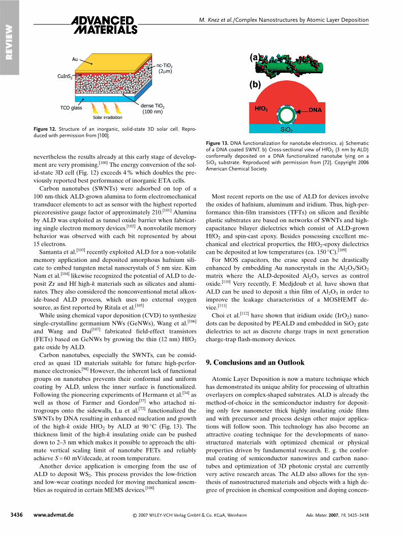
nevertheless the results already at this early stage of develop-ment are very promising.[100] The energy conversion of the sol-id-state 3D cell (Fig. 12) exceeds 4 % which doubles the pre-viously reported best performance of inorganic ETA cells.
Carbon nanotubes (SWNTs) were adsorbed on top of a100 nm-thick ALD-grown alumina to form electromechanicaltransducer elements to act as sensor with the highest reportedpiezoresistive gauge factor of approximately 210.[101] Aluminaby ALD was exploited as tunnel oxide barrier when fabricat-ing single electron memory devices.[102] A nonvolatile memorybehavior was observed with each bit represented by about15 electrons.
Samanta et al.[103] recently exploited ALD for a non-volatilememory application and deposited amorphous hafnium sili-cate to embed tungsten metal nanocrystals of 5 nm size. KimNam et al.[104] likewise recognized the potential of ALD to de-posit Zr and Hf high-k materials such as silicates and alumi-nates. They also considered the nonconventional metal alkox-ide-based ALD process, which uses no external oxygensource, as first reported by Ritala et al.[105]
While using chemical vapor deposition (CVD) to synthesizesingle-crystalline germanium NWs (GeNWs), Wang et al.[106]
and Wang and Dai[107] fabricated field-effect transistors(FETs) based on GeNWs by growing the thin (12 nm) HfO2
gate oxide by ALD.Carbon nanotubes, especially the SWNTs, can be consid-
ered as quasi 1D materials suitable for future high-perfor-mance electronics.[98] However, the inherent lack of functionalgroups on nanotubes prevents their conformal and uniformcoating by ALD, unless the inner surface is functionalized.Following the pioneering experiments of Hermann et al.[34] aswell as those of Farmer and Gordon[37] who attached ni-trogroups onto the sidewalls, Lu et al.[72] functionalized theSWNTs by DNA resulting in enhanced nucleation and growthof the high-k oxide HfO2 by ALD at 90 °C (Fig. 13). Thethickness limit of the high-k insulating oxide can be pusheddown to 2–3 nm which makes it possible to approach the ulti-mate vertical scaling limit of nanotube FETs and reliablyachieve S = 60 mV/decade, at room temperature.
Another device application is emerging from the use ofALD to deposit WS2. This process provides the low-frictionand low-wear coatings needed for moving mechanical assem-blies as required in certain MEMS devices.[108]
Most recent reports on the use of ALD for devices involvethe oxides of hafnium, aluminum and iridium. Thus, high-per-formance thin-film transistors (TFTs) on silicon and flexibleplastic substrates are based on networks of SWNTs and high-capacitance bilayer dielectrics which consist of ALD-grownHfO2 and spin-cast epoxy. Besides possessing excellent me-chanical and electrical properties, the HfO2-epoxy dielectricscan be deposited at low temperatures (ca. 150 °C).[109]
For MOS capacitors, the erase speed can be drasticallyenhanced by embedding Au nanocrystals in the Al2O3/SiO2
matrix where the ALD-deposited Al2O3 serves as controloxide.[110] Very recently, F. Medjdoub et al. have shown thatALD can be used to deposit a thin film of Al2O3 in order toimprove the leakage characteristics of a MOSHEMT de-vice.[111]
Choi et al.[112] have shown that iridium oxide (IrO2) nano-dots can be deposited by PEALD and embedded in SiO2 gatedielectrics to act as discrete charge traps in next generationcharge-trap flash-memory devices.
9. Conclusions and an Outlook
Atomic Layer Deposition is now a mature technique whichhas demonstrated its unique ability for processing of ultrathinoverlayers on complex-shaped substrates. ALD is already themethod-of-choice in the semiconductor industry for deposit-ing only few nanometer thick highly insulating oxide filmsand with precursor and process design other major applica-tions will follow soon. This technology has also become anattractive coating technique for the developments of nano-structured materials with optimized chemical or physicalproperties driven by fundamental research. E. g. the confor-mal coating of semiconductor nanowires and carbon nano-tubes and optimization of 3D photonic crystal are currentlyvery active research areas. The ALD also allows for the syn-thesis of nanostructured materials and objects with a high de-gree of precision in chemical composition and doping concen-
REV
IEW
M. Knez et al./Complex Nanostructures by Atomic Layer Deposition
3436 www.advmat.de © 2007 WILEY-VCH Verlag GmbH & Co. KGaA, Weinheim Adv. Mater. 2007, 19, 3425–3438
Figure 12. Structure of an inorganic, solid-state 3D solar cell. Repro-duced with permission from [100].
Figure 13. DNA functionalization for nanotube electronics. a) Schematicof a DNA coated SWNT. b) Cross-sectional view of HfO2 (3 nm by ALD)conformally deposited on a DNA functionalized nanotube lying on aSiO2 substrate. Reproduced with permission from [72]. Copyright 2006American Chemical Society.

tration. The developments of low-temperature deposition pro-cesses (< 100 °C) have significantly enlarged the applicationrange of ALD and the method was already applied on tem-perature-sensitive materials, like biomolecules and polymernanostructures. ALD of polymer films has recently been dem-onstrated for polyimides[113] and the process development willmost probably be extended to other organic coatings in nearfuture. Another specific feature of ALD, besides the capabili-ty of conformal deposition on non-planar surfaces, is a certaindegree of selectivity for depositions on patterned surfaces,which gives additional opportunities for nanostructured mate-rials synthesis. In addition to the booming activities on the de-positions of high-k dielectrics for the semiconductor industry,the application of ALD in combination with nanostructuredmaterials for conventional optics, solar cells, fuel cells, nano-particle coatings and jewellery is intensively under discussionand in some cases has already reached the commercial stage.
Received: January 10, 2007Revised: May 31, 2007
Published online: October 2, 2007
–[1] T. Suntola, J. Antson, US Patent 4 058 430, 1977.[2] L. Niinistö, Ann. Chim. 1997, 87, 221.[3] M. Leskelä, M. Ritala, Angew. Chem. Int. Ed. 2003, 42, 5548.[4] L. Niinistö, J. Päiväsaari, J. Niinistö, M. Putkonen, M. Nieminen,
Phys. Status Solidi A 2004, 201, 1443.[5] H. Kim, P. C. McIntyre, J. Korean Phys. Soc. 2006, 48, 5.[6] R. Puurunen, J. Appl. Phys. 2005, 97, 121 301.[7] H. Kim, J. Vac. Sci. Technol. B 2003, 21, 2231.[8] M. Leskelä, M. Kemell, K. Kukli, V. Pore, E. Santala, M. Ritala,
J. Lu, Mater. Sci. Eng. C 2007, 27, 1504.[9] International Technology Road Map for Semiconductors, http://pub-
lic.itrs.net/ (accessed September 2007).[10] C. Düsco, N. Q. Khanh, Z. Horvath, I. Barsony, M. Utriainen, S. Lehto,
M. Nieminen, L. Niinistö, J. Electrochem. Soc. 1996, 143, 683.[11] R. G. Gordon, D. Hausmann, E. Kim, J. Shepard, Chem. Vap. De-
position 2003, 9, 73.[12] J. E. Herrera, J. H. Kwak, J. Z. Hu, Y. Wang, C. H. F. Peden, Top.
Catal. 2006, 39, 245.[13] J. W. Elam, D. Routkevich, P. P. Mardilovich, S. M. George, Chem.
Mater. 2003, 15, 3507.[14] S. O. Kucheyev, J. Biener, Y. M. Wang, T. F. Baumann, K. J. Wu,
T. van Buuren, A. V. Hamza, J. H. Satcher, Jr., J. W. Elam, M. J. Pel-lin, Appl. Phys. Lett. 2005, 86, 083 108.
[15] T. F. Baumann, J. Biener, Y. M. Wang, S. O. Kucheyev, E. J. Nelson,J. H. Satcher, J. W. Elam, M. J. Pellin, A. V. Hamza, Chem. Mater.2006, 18, 6106.
[16] J. Biener, T. F. Baumann, Y. M. Wang, E. J. Nelson, S. O. Kucheyev,A. V. Hamza, M. Kemell, M. Ritala, M. Leskelä, Nanotechnology2007, 18, 055 303.
[17] M. S. Sander, M. J. Cote, W. Gu, B. M. Kile, C. P. Tripp, Adv. Mater.2004, 16, 2052.
[18] C. J. Yang, S.-M. Wang, S.-W. Liang, Y.-H. Chang, C. Chen, Appl.Phys. Lett. 2007, 90, 033 104.
[19] L. K. Tan, A. S. M. Chong, X. S. E. Tang, H. Gao, J. Phys. Chem. C2007, 111, 4964.
[20] M. Kemell, V. Pore, J. Tupala, M. Ritala, M. Leskelä, Chem. Mater.2007, 19, 1816.
[21] H. Shin, J. K. Jeong, J. Lee, M. M. Sung, J. Kim, Adv. Mater. 2004,16, 1197.
[22] M. Rooth, A. Johansson, M. Boman, A. Hårsta, Mater. Res. Soc.Symp. Proc. 2006, 901, Ra24–05.1.
[23] B. S. Lim, A. Rahtu, R. G. Gordon, Nat. Mater. 2003, 2, 749.[24] A. Johansson, T. Törndahl, L. M. Ottosson, M. Boman, J.-O. Carls-
son, Mater. Sci. Eng. C 2003, 23, 823.[25] M. Utriainen, M. Kröger-Laukkanen, L.-S. Johansson, L. Niinistö,
Appl. Surf. Sci. 2000, 137, 151.[26] M. Daub, M. Knez, U. Gösele, K. Nielsch, J. Appl. Phys. 2007, 101,
09J111.[27] Z. Li, R. G. Gordon, Chem. Vap. Deposition 2006, 12, 435.[28] P. Cheng, T. Mitsui, D. P. Farmer, J. Golovchenko, R. G. Gordon,
D. Branton, Nano Lett. 2004, 4, 1333.[29] H. J. Fan, P. Werner, M. Zacharias, Small 2006, 2, 700.[30] M. T. Björk, B. J. Ohlsson, T. Sass, A. I. Persson, C. Thelander,
M. H. Magnusson, K. Deppert, L. R. Wallenberg, L. Samuelson,Nano Lett. 2002, 2, 87.
[31] R. Solanki, J. Huo, J. L. Freeouf, B. Miner, Appl. Phys. Lett. 2002,81, 3864.
[32] G. Kipshidze, B. Yavich, A. Chandolu, J. Yon, V. Kuryatkov, I. Ah-mad, D. Aurongzeb, M. Holz, H. Temkin, Appl. Phys. Lett. 2005, 86,033 104.
[33] D. Zhang, S. Moore, J. Wei, A. Alkhateeb, D. Gangadean, H. Mah-mood, J. Lantrips, D. N. McIlroy, A. D. LaLonde, M. G. Norton, J. S.Young, C. Wang, Appl. Phys. Lett. 2005, 86, 263 110.
[34] C. F. Hermann, F. H. Fabreguette, D. S. Finch, R. Geiss, S. M.George, Appl. Phys. Lett. 2005, 87, 123 110.
[35] D. B. Farmer, R. G. Gordon, Nano Lett. 2006, 6, 699.[36] Y. S. Min, E. J. Bae, K. S. Jeong, Y. J. Cho, J. H. Lee. W. B. Choi,
G. S. Park, Adv. Mater. 2003, 15, 1019.[37] D. B. Farmer, R. G. Gordon, Electrochem. Solid-State Lett. 2005, 8,
G89.[38] D. Wang, Y. L. Chang, Q. Wang, J. Cao, D. B. Farmer, R. G. Gordon,
H. Dai, J. Am. Chem. Soc. 2004, 126, 11 602.[39] a) H. J. Fan, M. Knez, R. Scholz, K. Nielsch, E. Pippel, D. Hesse,
M. Zacharias, U. Gösele, Nat. Mater. 2006, 5, 627. b) H. J. Fan,M. Knez, R. Scholz, D. Hesse, K. Nielsch, M. Zacharias, U. Gösele,Nano Lett. 2007, 7, 993.
[40] H. J. Fan, M. Knez, R. Scholz, K. Nielsch, E. Pippel, D. Hesse,U. Gösele, M. Zacharias, Nanotechnology 2006, 17, 5157.
[41] B. Min, J. S. Lee, J. W. Hwang, K. H. Keem, M. I. Kang, K. Cho,M. Y. Sung, S. Kim, M.-S. Lee, S. O. Park, J. T. Moon, J. Cryst.Growth 2003, 252, 565.
[42] M. Law, L. E. Greene, A. Radenovic, T. Kuykendall, J. Liphardt,P. Yang, J. Phys. Chem. B 2006, 110, 22 652.
[43] J. F. Conley, L. Strecker, Y. Ono, Appl. Phys. Lett. 2005, 87, 223 114.[44] T. Nishida, N. Kobayashi, T. Ban, Appl. Phys. Lett. 2002, 82, 1.[45] M. Kang, J.-S. Lee, S.-K. Sim, B. Min, K. Cho, H. Kim, M.-Y. Sung,
S. Kim, S. A. Song, M.-S. Lee, Thin Solid Films 2004, 466, 265.[46] M. J. Biercuk, D. J. Monsma, C. M. Marcus, J. S. Becker, R. G. Gor-
don, Appl. Phys. Lett. 2003, 83, 2405.[47] K. S. Park, E. K. Seo, Y. R. Do, K. Kim, M. M. Sung, J. Am. Chem.
Soc. 2006, 128, 858.[48] E. K. Seo, J. W. Lee, S. M. Hyung, M. M. Sung, Chem. Mater. 2004,
16, 1878.[49] K. J. Park, J. M. Doub, T. Gougousi, G. N. Parsons, Appl. Phys. Lett.
2005, 86, 051 903.[50] J. P. Lee, M. M. Sung, J. Am. Chem. Soc. 2004, 126, 28.[51] R. Chen, H. Kim, P. C. McIntyre, D. W. Porter, S. F. Bent, Appl.
Phys. Lett. 2005, 86, 191 910.[52] R. Chen, S. F. Bent, Adv. Mater. 2006, 18, 1086.[53] A. V. Whitney, J. W. Elam, S. Zou, A. V. Zinovev, P. C. Stair, G. C.
Schatz, R. P. van Duyne, J. Phys. Chem. B 2005, 109, 20 522.[54] X. D. Wang, E. Graugnard, J. S. King, Z. L. Wang, C. J. Summers,
Nano Lett. 2004, 4, 2223.[55] E. Graugnard, J. S. King, D. P. Gaillot, C. J. Summers, Adv. Funct.
Mater. 2006, 16, 1187.[56] C. A. Wilson, R. K. Grubbs, S. M. George, Chem. Mater. 2005, 17,
5625.
REV
IEWM. Knez et al./Complex Nanostructures by Atomic Layer Deposition
Adv. Mater. 2007, 19, 3425–3438 © 2007 WILEY-VCH Verlag GmbH & Co. KGaA, Weinheim www.advmat.de 3437
[57] X. Liang, L. F. Hakim, G.-D. Zhan, J. A. McCormick, S. M. George,A. W. Winter, J. Am. Ceram. Soc. 2007, 90, 57.
[58] W. Gasser, Y. Uchida, M. Matsumura, Thin Solid Films 1994, 250,213.
[59] J. W. Klaus, O. Sneh, S. M. George, Science 1997, 278, 1934.[60] Y. Luo, D. Slater, M. Han, J. Moryl, R. M. Osgood, Appl. Phys. Lett.
1997, 71, 3799.[61] M. D. Groner, F. H. Fabreguette, J. W. Elam, S. M. George, Chem.
Mater. 2004, 16, 639.[62] J. D. Ferguson, A. W. Weimer, S. M. George, Chem. Mater. 2004, 16,
5602.[63] R. H. A. Ras, M. Kemell, J. De Wit, M. Ritala, G. Ten Brinke,
M. Leskelä, O. Ikkala, Adv. Mater. 2007, 19, 102.[64] Q. Peng, X.-Y. Sun, J. C. Spagnola, G. K. Hyde, R. J. Spontak, G. N.
Parsons, Nano Lett. 2007, 7, 719.[65] M. Knez, A. Kadri, C. Wege, U. Gösele, H. Jeske, K. Nielsch, Nano
Lett. 2006, 6, 1172.[66] J. Huang, X. Wang, Z. L. Wang, Nano Lett. 2006, 6, 2325.[67] M. Kemell, V. Pore, M. Ritala, M. Leskelä, M. Linden, J. Am. Chem.
Soc. 2005, 127, 14 178.[68] J. W. Klaus, S. M. George, Surf. Sci. 2000, 447, 81.[69] J. S. King, E. Graungnard, O. M. Roche, D. N. Sharp, J. Scrimgeour,
R. G. Denning, A. J. Turberfield, C. J. Summers, Adv. Mater. 2006,18, 1561.
[70] M. Putkonen, L. Niinistö, Thin Solid Films 2006, 514, 145.[71] J. Keränen, C. Guimon, E. Iiskola, A. Auroux, L. Niinistö, J. Phys.
Chem. B 2003, 107, 10 773.[72] Y. Lu, S. Bangsaruntip, X. Wang, L. Zhang, Y. Nishi, H. Dai, J. Am.
Chem. Soc. 2006, 128, 3518.[73] M. Scharrer, X. Wu, A. Yamilov, H. Cao, R. P. H. Chang, Appl.
Phys. Lett. 2005, 86, 151 113.[74] G. A. Ten Eyck, S. Pimanpang, H. Bakhru, T. M. Lu, G. C. Wang,
Chem. Vap. Deposition 2006, 12, 290.[75] G. A. Ten Eyck, J. J. Senkevich, F. Tang, D. Liu, S. Pimanpang,
T. Karaback, G. C. Wang, T. M. Lu, C. Jezewski, W. A. Lanford,Chem. Vap. Deposition 2005, 11, 60.
[76] A. Birner, R. B. Wehrspohn, U. Gösele, K. Busch, Adv. Mater. 2001,13, 377.
[77] S. Matthias, F. Müller, C. Jamois, R. B. Wehrspohn, U. Gösele, Adv.Mater. 2004, 16, 2166.
[78] P. V. Braun, S. A. Rinne, F. Garvia-Santamaria, Adv. Mater. 2006, 18,2665.
[79] H. M. Yates, M. E. Pemble, H. Miguez, A. Blanco, C. Lopez, F. Me-seguer, L. Vazquez, J. Cryst. Growth 1998, 193, 9.
[80] A. Blanco, E. Chomski, S. Grabtchak, M. Ibisate, S. John, S. W. Leo-nard, C. Lopez, F. Meseguer, H. Miguez, J. P. Mondia, G. A. Ozin,O. Toader, H. M. van Driel, Nature 2000, 405, 437.
[81] F. G. Fleming, S. Y. Lin, I. El-Kady, R. Biswas, K. M. Ho, Nature2002, 417, 52.
[82] N. Tétreault, G. von Freymann, M. Deubel, M. Hermatschweiler,F. Pérez-Willard, S. John, M. Wegener, G. A. Ozin, Adv. Mater. 2006,18, 457.
[83] A. Rugge, J. S. Becker, R. G. Gordon, S. H. Tolbert, Nano Lett.2003, 3, 1293.
[84] J. S. King, C. W. Neff, C. J. Summers, W. Park, S. Blomquist, E. For-sythe, D. Morton, Appl. Phys. Lett. 2003, 83, 2566.
[85] J. S. King, C. W. Neff, S. Blomquist, E. Forsythe, D. Morton, C. J.Summers, Phys. Status Solidi B 2004, 241, 763.
[86] J. S. King, E. Graungnard, C. J. Summers, Adv. Mater. 2005, 17, 1010.[87] A. Rugge, J. S. Park, R. G. Gordon, S. H. Tolbert, J. Phys. Chem. B
2005, 109, 3765.[88] M. Scharrer, A. Yamilov, X. Wu, H. Cao, R. P. H. Chang, Appl.
Phys. Lett. 2006, 88, 201 103.[89] I. M. Povey, D. Whitehead, K. Thomas, M. E. Pemble, M. Bardoso-
va, J. Renard, Appl. Phys. Lett. 2006, 89, 104 103.[90] Z. A. Sechrist, B. T. Schwartz, J. H. Lee, J. A. McCormick, R. Pies-
tum, W. Park, S. M. George, Chem. Mater. 2006, 18, 3562.[91] J. S. King, E. Graugnard, C. J. Summers, Appl. Phys. Lett. 2006, 88,
081 109.[92] X. Wang, C. Neff, E. Graungnard, Y. Ding, J. S. King, L. A. Pranger,
R. Tannenbaum, Z. L. Wang, C. J. Summers, Adv. Mater. 2005, 17,2103.
[93] R. M. Costescu, D. G. Cahill, F. H. Fabreguette, Z. A. Sechrist,S. M. George, Science 2004, 303, 989.
[94] Z. A. Sechrist, F. H. Fabreguette, O. Heintz, T. M. Phung, D. C.Johnson, S. M. George, Chem. Mater. 2005, 17, 3475.
[95] J. J. Wang, X. Deng, R. Varghese, A. Nikolov, P. Sciortino, F. Liu,L. Chen, X. Liu, J. Vac. Sci. Technol. B 2005, 23, 3209.
[96] J. J. Wang, A. Nikolov, Q. Wu, IEEE Photonics Technol. Lett. 2006,18, 2650.
[97] A. Javey, H. Kim, M. Brink, Q. Wang, A. Ural, J. Guo, P. McIntyre,P. McEuen, M. Lundstrom, H. Dai, Nat. Mater. 2002, 1, 241.
[98] A. Javey, J. Guo, D. B. Farmer, Q.Wang, E. Yenilmez, R. G. Gordon,M. Lundstrom, H. Dai, Nano Lett. 2004, 4, 1319.
[99] K. Keem, D.-Y. Jeong, S. Kim, M.-S. Lee, I.-S. Yeo, U.-I. Shung, J.-T.Moon, Nano Lett. 2006, 6, 1451.
[100] M. Nanu, J. Schoonman, A. Gossens, Adv. Mater. 2004, 16, 453.[101] G. Stampfer, T. Helbling, D. Obergfell, B. Schöberle, M. K. Tripp,
A. Jungen, S. Roth, V. M. Bright, C. Hierold, Nano Lett. 2006, 6,233.
[102] K. K. Yadawalli, N. R. Anderson, T. A. Orlova, A. O. Orlov, G. L.Snider, J. Elam, J. Vac. Sci. Technol. B 2004, 22, 3119.
[103] S. Samanta, Z. Y. L. Tan, W. J. Woo, G. Samudra, S. Lee, L. K. Bera,N. Balasubramanian, J. Vac. Sci. Technol. B 2005, 23, 2278.
[104] W. K. Kim, W. H. Nam, S. H. Kim, S. H. Rhee, J. Chem. Eng. Jpn.2005, 38, 578.
[105] M. Ritala, K. Kukli, A. Rahtu, P. I. Räisänen, M. Leskelä, T. Saja-vaara, J. Keinonen, Science 2000, 288, 319.
[106] D.Wang, Q. Wang, A. Javey, R. Tu, H. Dai, H. Kim, P. C. McIntyre,T. Krisnamohan, K. C. Saraswat, Appl. Phys. Lett. 2003, 83, 2432.
[107] D. Wang, H. Dai, Appl. Phys. A 2006, 85, 217.[108] T. W. Scharf, S. V. Prasad, M. T. Dugger, P. G. Kotula, R. S. Goeke,
R. K. Grubbs, Acta Mater. 2006, 54, 4731.[109] Q. Cao, M.-G. Xia, M. Shim, J. A. Rogers, Adv. Funct. Mater. 2006,
16, 2355.[110] C.-C. Wang, Y.-K. Chiou, C.-H. Chang, J.-Y. Tseng, C.-Y. Chen, T.-B.
Wu, J. Phys. D 2007, 40, 1673.[111] F. Medjdoub, N. Sarazin, M. Tordjman, M. Magis, M. A. di Forte-
Poisson, M. Knez, E. Delos, C. Gaquiere, S. L. Delage, E. Kohn,IEEE Electron. Device Lett. 2007, 43, 691.
[112] S. Soi, Y.-K. Cha, B.-S. Seo, S. Park, J.-H. Park, S. Shin, K. S. Seol,J.-B. Park, Y.-Park, Y. Park, I.-K. Yoo, S. H. Choi, J. Phys. D 2007,40, 1426.
[113] M. Putkonen, J. Harjuoja, T. Sajavaara, L. Niinistö, J. Mater. Chem.2007, 17, 664.
______________________
REV
IEW
M. Knez et al./Complex Nanostructures by Atomic Layer Deposition
3438 www.advmat.de © 2007 WILEY-VCH Verlag GmbH & Co. KGaA, Weinheim Adv. Mater. 2007, 19, 3425–3438