synthesis of metal oxide nanostructure and its ... · pdf filesynthesis of metal oxide...
TRANSCRIPT
Synthesis of metal oxide nanostructure and its characterization as gas pollutant monitoring
B. Yuliarto, M. Faizal, M. Iqbal, S. Julia & T. Nugraha Processing Materials Laboratory, Department of Engineering Physics, Institut Teknologi Bandung (ITB), Bandung, Indonesia
Abstract
The characteristics of metal oxide thin films have been studied for gas pollutant monitoring systems. The metal oxide sensitive layers of ZnO are deposited by sol gel method using a chemical bath deposition technique at moderate temperature. The resulting thin films have been characterized using XRD and SEM to confirm the surface structure of the film. The scanning electron microscopy reveals that ZnO thin films have a nanostructure morphology which is supposed to open a larger area to the gas targeted. The sensor device was prepared using alumina as a substrate and a gold finger electrode on the top of the sensors. Gas pollutant monitoring systems have been developed using the resulting sensor device after the calibrating process. The gas monitoring system can measure and save the data in the system so that the trend of measured pollutant can be analyzed for a certain period of time. The design and electronics structure of the gas pollutant monitoring system in terms of CO emission are described. This monitoring system can be used as a sensing node and can form a dense real-time environmental monitoring network. Keywords: thin film, ZnO, CO, gas pollutants, nanostructure, monitoring, sensors.
1 Introduction
In recent times there have been growing concerns about the consequences of air pollution on our atmosphere. This growing awareness is enhanced because atmospheric pollution is not only an environmental problem but also induces serious health hazards on humans. Air pollution emerged around the world in the last decade as a result of explosive industrial growth. After that, efforts were
Air Pollution XIX 231
www.witpress.com, ISSN 1743-3541 (on-line) WIT Transactions on Ecology and the Environment, Vol 147, © 2011 WIT Press
doi:10.2495/AIR110211

made to monitor and reduce the emission of pollutants resulting from factories and industrial areas, as well as vehicles. In many countries, there has been a regulation to establish a network of environmental quality monitoring stations, especially in their main cities, to give information and record the data about the environmental quality on a regular basis. However, there have been several limitations of the stations including the high price and lengthy air sampling data. The measurement technique used to detect the pollutants gas is passive samplers or a commercially spectroscopic gas analyzer yield longer and non on time monitoring systems. A gas sensor based on metal oxide should be developed so that the sensor can detect in situ and real time response. Moreover, the nanostructure of the ZnO thin films would give an advantage of having large accessibility for the targeted gases [1–4]. This research proposes the design and fabrications of gas pollutant monitoring systems based on ZnO nanostructure thin films. The using of ZnO is based on others’ research which shows that the thin films of ZnO find many promising applications due to their eccentric properties including a large exciton bonding energy of 60 MeV, non-toxicity, good electrical, optical and piezoelectrical behavior, and low cost [5–7]. ZnO is particularly attractive to researchers to be used as a sensor because ZnO has the desired and required typical properties such as resistivity control over the range 10-3–105 Mohm cm, excellent thermal and electrical stability. Here, we present the preparation of ZnO nanostructures thin films on an alumina substrate. The substrates were printed onto a silver finger electrode before the ZnO is deposited. The resulting sensor devices have been constructed as a real time monitoring system. The ZnO surface properties have been studied and the effects on the sensing performance have been measured. The sensitivity of pollutants in terms of CO gas has been measured in different operating temperatures.
2 Experiments
A thin layer was deposited by chemical bath deposition (CBD) on alumina substrates that have been cleaned. The solution was synthesized from zinc nitrate tetrahydrate and the dissolving of urea in the DI water. Zinc nitrate tetrahydrate, Iron (III) nitrate nonahydrate, and DI water + ethanol were dissolved at room temperature and stirred using a magnetic stirrer for 30 minutes. Urea is added to the solution and stirred for 30 minutes to produce a homogeneous solution. Alumina substrate has been cleaned up, immersed and placed in a standing position in a clear solution. Substrates were immersed in clear CBD solution, kept in the furnace at a temperature of 60oC for 24 hours. Substrates that have been deposited are removed from the place of immersion and washed using acetone to stop the growth of crystals. Then the films were rinsed in DI water several times and dried at room temperature for one hour in air atmosphere. A transformation into ZnO was conducted by calcination of the films at 300oC in air atmosphere for 30 minutes with 20oC/minute heat rate [10]. X-ray Diffraction (XRD), and Scanning Electron Microscopy (SEM) were employed to study the
232 Air Pollution XIX
www.witpress.com, ISSN 1743-3541 (on-line) WIT Transactions on Ecology and the Environment, Vol 147, © 2011 WIT Press
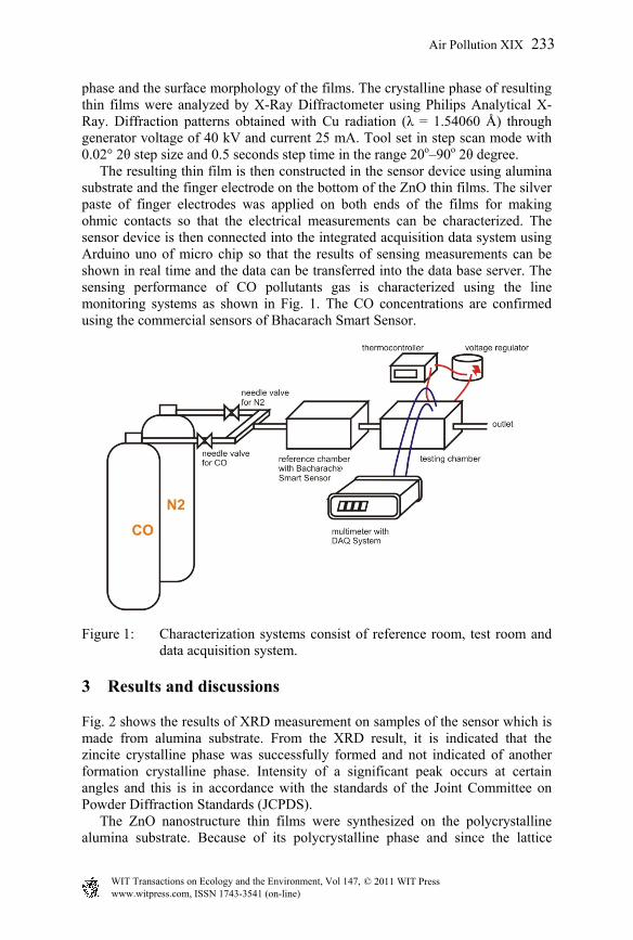
phase and the surface morphology of the films. The crystalline phase of resulting thin films were analyzed by X-Ray Diffractometer using Philips Analytical X-Ray. Diffraction patterns obtained with Cu radiation (λ = 1.54060 Å) through generator voltage of 40 kV and current 25 mA. Tool set in step scan mode with 0.02° 2θ step size and 0.5 seconds step time in the range 20o–90o 2θ degree. The resulting thin film is then constructed in the sensor device using alumina substrate and the finger electrode on the bottom of the ZnO thin films. The silver paste of finger electrodes was applied on both ends of the films for making ohmic contacts so that the electrical measurements can be characterized. The sensor device is then connected into the integrated acquisition data system using Arduino uno of micro chip so that the results of sensing measurements can be shown in real time and the data can be transferred into the data base server. The sensing performance of CO pollutants gas is characterized using the line monitoring systems as shown in Fig. 1. The CO concentrations are confirmed using the commercial sensors of Bhacarach Smart Sensor.
Figure 1: Characterization systems consist of reference room, test room and data acquisition system.
3 Results and discussions
Fig. 2 shows the results of XRD measurement on samples of the sensor which is made from alumina substrate. From the XRD result, it is indicated that the zincite crystalline phase was successfully formed and not indicated of another formation crystalline phase. Intensity of a significant peak occurs at certain angles and this is in accordance with the standards of the Joint Committee on Powder Diffraction Standards (JCPDS). The ZnO nanostructure thin films were synthesized on the polycrystalline alumina substrate. Because of its polycrystalline phase and since the lattice
Air Pollution XIX 233
www.witpress.com, ISSN 1743-3541 (on-line) WIT Transactions on Ecology and the Environment, Vol 147, © 2011 WIT Press
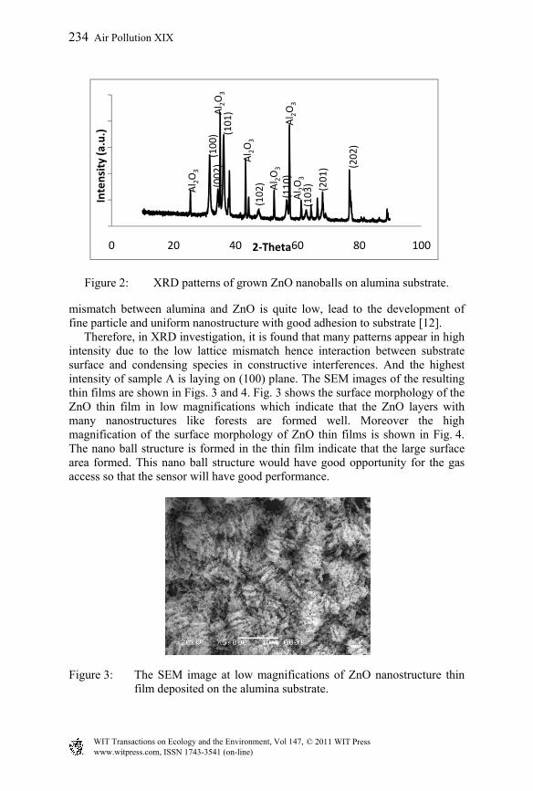
Figure 2: XRD patterns of grown ZnO nanoballs on alumina substrate.
mismatch between alumina and ZnO is quite low, lead to the development of fine particle and uniform nanostructure with good adhesion to substrate [12]. Therefore, in XRD investigation, it is found that many patterns appear in high intensity due to the low lattice mismatch hence interaction between substrate surface and condensing species in constructive interferences. And the highest intensity of sample A is laying on (100) plane. The SEM images of the resulting thin films are shown in Figs. 3 and 4. Fig. 3 shows the surface morphology of the ZnO thin film in low magnifications which indicate that the ZnO layers with many nanostructures like forests are formed well. Moreover the high magnification of the surface morphology of ZnO thin films is shown in Fig. 4. The nano ball structure is formed in the thin film indicate that the large surface area formed. This nano ball structure would have good opportunity for the gas access so that the sensor will have good performance.
Figure 3: The SEM image at low magnifications of ZnO nanostructure thin film deposited on the alumina substrate.
0 20 40 60 80 100
Intensity (a.u.)
2‐Theta
(100) (1
01)
(110)
Al 2O3
Al 2O3
(102)(002) (202)
Al 2O3
Al 2O3
Al 2O3
(201)
Al 2O3
(103)
234 Air Pollution XIX
www.witpress.com, ISSN 1743-3541 (on-line) WIT Transactions on Ecology and the Environment, Vol 147, © 2011 WIT Press

Figure 4: High magnifications SEM images of nanoballs in the range of 250nm.
The ZnO nanostructure sensor is constructed in the gas pollutant monitoring system which can report the result in real time and regularly update the display on the web site. The complete diagram structure of the gas pollutant monitoring systems can be seen in Fig. 5.
Figure 5: The real time monitoring systems based on ZnO nanostructure thin film.
The sensor of ZnO nanostructure thin film (block diagram #1) detects the presence of the target gas in air (CO) in the certain concentration. In order that the sensor can work optimally, it requires a basic measurement circuit as shown in block diagram of no. 2. This circuit heats the internal heater sensor up to a certain temperature (around 200oC) so that the sensor can measure the target gas at its best performance. The output from these sensors, which is in voltage, is still an analog signal. Before it is converted into a digital signal, the analog signal needs to be adjusted to fit the input range of the microcontroller (Arduino Uno) whose range is between 0–5 volts. These adjustments use the op-amplifier as a voltage amplifier mounted on the basic measurement circuit. The A/D converter utilizing Analog input pin of Arduino Uno (block diagram #3) is used to convert into a digital signal. We set pin A0 and A5 as input of CO yielded from the sensors. After that, through the Arduino software, we compiled into digital signals (ppm value) which then displayed in parallel on the LCD screen (block diagram No. 4) and displayed to the website via DFR Duino ethernet
Air Pollution XIX 235
www.witpress.com, ISSN 1743-3541 (on-line) WIT Transactions on Ecology and the Environment, Vol 147, © 2011 WIT Press

shield which is connected to the server by LAN’s cable network type RG45 (block diagram # 5). Fig. 6 shows the sensor characteristics of response dynamics at 600 ppm and 300 ppm of the gas CO. The measurements are performed at 200oC. The clear decreasing at significant levels both on 300 ppm and 600 ppm are happened suddenly after the explosions of the CO gas. The change of resistivity value indicates that the sensor has good sensitivity as well as fast response time both in 300 ppm and 600 ppm of CO gas. When a metal oxide semiconductor of ZnO nanostructure thin film is heated at a certain high temperature in air, oxygen is adsorbed on the semiconductor surface with a negative charge. Then donor electrons in the semiconductor surface are transferred to the adsorbed oxygen, resulting in leaving positive charges in a space charge layer. Thus, surface potential is formed to serve as a potential barrier against electron flow. Inside the sensor, electric current flows through the conjunction parts (grain boundary) of ZnO micro crystals. At grain boundaries, adsorbed oxygen forms a potential barrier which prevents carriers from moving freely. The electrical resistance of the sensor is attributed to this potential barrier. In the presence of a deoxidizing gas, the surface density of the negatively charged oxygen decreases, so the potential barrier in the grain boundary is reduced. The reduced potential barrier decreases sensor resistance.
Figure 6: The response dynamics of ZnO nanostructure thin film.
4 Conclusions
The synthesis process of chemical bath deposition technique has been performed successfully to grow the ZnO thin film on the alumina structure. The resulting ZnO thin film have the nano ball structure which yield good accessibility for the targeted CO gas adsorbed to the surface of the ZnO sensitive layer. The sensors
0
5
10
15
20
25
30
0 5 10 15 20 25 30 35 40 45
Response (%)
Time (Minutes)
300ppm
600 ppm
CO OFFCO ON
236 Air Pollution XIX
www.witpress.com, ISSN 1743-3541 (on-line) WIT Transactions on Ecology and the Environment, Vol 147, © 2011 WIT Press

have good sensitivity on the exposure of CO gas at 300 ppm and 600 ppm. The on line and real time measurement systems have been constructed so that the sensors can be performed as the pollutant monitoring system.
References
[1] Z.I. Wang, Nanostructure of zinc oxide. Matter. Today, 7(6), pp. 26-33, 2004.
[2] D. Calestani, M. Zha, R. Mosca, A. Zappettini, M.C. Carotta, V. Di Natale, L. Zanotti, Growth of ZnO tetrapods for nanostructure-based gas sensors. Sensors and Actuators B, 144, pp. 472-478, 2010.
[3] B. Yuliarto, Y. Kumai, S. Inagaki, HS. Zhou, Enhanced benzene selectivity of mesoporous silica SPV sensors by incorporating phenylene groups in the silica framework, Sensors and Actuators B: Chemical, 138 Issue 2, pp. 417-421, 2009.
[4] M.A. Lim, Y.W. Lee, S.W. Han, I. Park, Novel fabrication method of diverse one-dimensional Pt/ZnO hybrid nanostructures and its sensor application, Nanotechnology, 22, 035601 pp. 8, 2011.
[5] C. Klingshirn, ZnO: from basics towards applications, Phys. Status Solidi B, 244, pp. 3027-3073, 2007.
[6] D.C. Look, D.C. Reynolds, J.W. Hemsky, R.L. Jones, J.R. Sizelove, Production and annealing of electron irradiation damage in ZnO, Appl. Phys. Lett., 75, pp. 811-813, 1999.
[7] F. Tuomisto, K. Saarinen, D.C. Look, Irradiation-induced defects in ZnO studied by positron annihilation spectroscopy, Phys. Status Solidi A, 201, pp. 2219-2224, 2004.
Air Pollution XIX 237
www.witpress.com, ISSN 1743-3541 (on-line) WIT Transactions on Ecology and the Environment, Vol 147, © 2011 WIT Press