synthesis of nano-structured materials by laser-ablation and their application to sensors
TRANSCRIPT

www.elsevier.com/locate/apsusc
Applied Surface Science 253 (2007) 7840–7847
Synthesis of nano-structured materials by laser-ablation
and their application to sensors
T. Okada *, J. Suehiro
Department of Electrical and Electronic Systems Engineering, Kyushu University, Fukuoka 812-8581, Japan
Available online 2 March 2007
Abstract
We describe the synthesis of nano-structured materials of ZnO and Pd by laser ablation and their applications to sensors. The synthesis of ZnO
nano-wires was performed by nano-particle assisted deposition (NPAD) where nano-crystals were grown with nano-particles generated by laser-
ablating a ZnO sintered target in an Ar background gas. The synthesized ZnO nano-wires were characterized with a scanning electron microscopy
and the photoluminescent characteristics were examined under an excitation with the third harmonics of a Nd:YAG laser. The nano-wires with a
diameter in the range from 50 to 150 nm and a length of up to 5 mm were taken out of the substrate by laser blow-off technique and/or sonication. It
was confirmed that the nano-wires showed the stimulated emission under optical pumping, indicating a high quality of the crystalinity. Pd nano-
particles were generated by laser-ablating a Pd plate in pure water. The transmission electron microscope observation revealed that Pd nano-
particles with a diameter in the range from 3 nm to several tens of nanometers were produced. Using these nano-structured materials, we
successfully fabricated sensors by the dielectrophoresis techniques. In the case of the ultraviolet photosensor, a detection sensitivity of 10 nW/cm2
was achieved and in the case of hydrogen sensing, the response time of less than 10 s has been demonstrated with Pd nano-particles.
# 2007 Elsevier B.V. All rights reserved.
Keywords: Nano-structure; Laser-ablation; Nd:YAG laser
1. Introduction
Recently the synthesis and the applications of nano-
structured materials have attracted a great attention. One of
the interesting materials is zinc oxides (ZnO), which are a wide-
band-gap II–VI semiconductor that has the direct band gap of
about 3.37 eV at room temperature, and is well recognized as
the functional material suitable for opto-electronic applica-
tions. In the past few years, nano-structured ZnO crystals, such
as nano-rods, nano-wires and nano-balls have been of growing
interest due to their importance both in scientific and
technological researches [1]. Considerable efforts have been
paid on the synthesis and on the study of nano-structured ZnO
crystals [2–4]. Several methods have been reported on the
synthesis of the ZnO nano-structured crystals, including vapor-
phase transport with a vapor–liquid–solid (VLS) growth
mechanism [5], wet chemical route [3], chemical vapor
deposition [6], nano-particle assisted deposition (NPAD)
* Corresponding author. Tel.: +81 92 642 3913; fax: +81 92 642 3965.
E-mail address: [email protected] (T. Okada).
0169-4332/$ – see front matter # 2007 Elsevier B.V. All rights reserved.
doi:10.1016/j.apsusc.2007.02.152
[7,8] and so on. One of the promising application field of
these nano-structured ZnO crystals is the sensors, in which a
large surface-to-volume ratio is essential for achieving higher
sensitivity. So far, ZnO nano-wires have been applied to the
ultraviolet photosensors [9], the ethanol sensors [10], the
oxygen sensors [11], the hydrogen sensor [12], the pH sensors
[13] and so on. Recently we have also successfully fabricated
an ultraviolet photo sensor with a high sensitivity using ZnO
nano-wires synthesized by NPAD [14].
From the viewpoint of gas sensor application, palladium (Pd)
has an interesting characteristic for the hydrogen molecules,
including the large capacity of hydrogen occlusion and the
catalysis effect for the reaction between hydrogen and oxygen at
room temperature. These characteristics of Pd are very attractive
for the hydrogen sensor and their sensitivities are also enhanced
by down-sizing into the nanometer range [15]. Therefore,
preparation of nano-structured Pd or other noble metals is also an
active research field, where chemical routes [15,16] and the laser
ablation of noble metal in a solution [17–19] has attracted a great
attention. More recently, Wang et al. reported the hydrogen
sensors using ZnO nano-wires covered with Pd and other noble
metals by sputtering deposition [20].

Fig. 2. SEM image of ZnO nano-wires grown on sapphire (0 0 0 1) substrates.
T. Okada, J. Suehiro / Applied Surface Science 253 (2007) 7840–7847 7841
Another subject, that should be considered in the application
of nano-structured materials to electronic devices like sensors,
is the handling of nano-materials in the fabrication of devices.
For instance, it is difficult task even to connect the electrodes
onto a nano-wire that is randomly placed on a substrate. One
sophisticated connection process includes the position sensing
of a nano-wire, the resist coating on it, the electron beam
lithography for the patterning of electrodes, the metal film
deposition and the lift-off [1]. They are the very complicated,
time consuming and expensive processes. We have recently
applied the dielectrophoresis technique (DEP) to collect the
carbon nano-tubes [21] and ZnO nano-wires onto the pattered
electrodes [14], demonstrating that the dielectrophoresis
technique is suitable for the mass production process.
In this paper, we describe our recent progresses of synthesis
of nano-structured materials of ZnO and Pd by laser ablation for
their applications to sensors. In Section 2, the preparations of
ZnO nano-wires by NPAD and of the Pd nano-particles by the
laser-ablation in pure water are described. In Section 3, the
handling of ZnO nano-wires and the sensor device fabrication
by DEP are described. Finally in Section 4, the characteristics
of an ultraviolet photosensor made by the ZnO nano-wires and
the possible application of the Pd nano-particles to the
hydrogen sensors are described.
2. Preparation of nano-structured materials
2.1. Preparation of ZnO nano-wires and their fluorescence
property
The apparatus used for ZnO growth is shown in Fig. 1 and it
is similar to that used for the synthesis of carbon nano-tubes by
laser ablation. It is a laser-ablation system in a high-temperature
background gas that has also been used to synthesize various
types of semiconductor nano-wires. A rotating ZnO sintered
target was laser-ablated by a KrF excimer laser in a quartz
furnace. The temperature of the furnace was varied in the range
from 870 K to 1470 K, which were measured by a thermo-
couple at an outer wall of the quartz tube. The KrF laser was
operated with an irradiation fluence of about 4 J/cm2 at a
repetition rate of 20 Hz. During the deposition, Ar gas at a
pressure in the range from about 30 and 60 kPa were flew with a
flow rate of 15 sccm. ZnO crystals were grown on the substrates
placed in front of the ZnO target, as shown in Fig. 1. ZnO
crystals were grown on sapphire (0 0 0 1) and (1 1 0 0)
substrates. Only when the substrates were placed between 10
and 30 mm in front of the target, appreciable amount of white
Fig. 1. Experimental appratus for synthesis of ZnO nano-structured crystals.
deposits was observed on the substrates. A variety of nano-
structured crystals was obtained by changing a kind of substrate
and the deposition conditions such as the furnace temperature,
gas pressure and so on [22].
ZnO nano-wires with a diameter of about 50 nm were
synthesized on sapphire (0 0 0 1) substrates. A SEM image of
the crystals is shown in Fig. 2 which was synthesized at an Ar
gas pressure of 34 kPa at 1070 K. It cannot be seen in the SEM
image, but hexagonal-shaped crystals exist between the nano-
wires and the substrate. When the (1 1 0 0) sapphire substrate
was used instead of (0 0 0 1) substrates, the ZnO cone-shaped
crystals perpendicular to the substrate surface was obtained at
an Ar pressure of 30 kPa and a substrate temperature of 1070 K,
as shown in Fig. 3. The similar effect of differently oriented
substrates on the ZnO crystal growth has been reported [23].
The ZnO cone-shaped crystals are very much interesting for the
application to the field emission [24], because of their unique
geometry for the field enhancement.
In the above studies, no catalyst was used to grow the ZnO
nano-wires and the relatively large hexagonal crystals always
exist between the nano-wires and the substrate. Therefore, it is
thought that the growth mechanism of ZnO nano-wires in the
present experiments is different from the VLS mechanism
with a help of catalyst. In the VLS mechanism, on the other
hand, the nano-wires grow directly from the substrate with the
catalysts on the other edge of the nano-wires. We believe that
Fig. 3. SEM image of ZnO nano-cone grown on sapphire (1 1 0 0) substrate.

Fig. 4. Growth model of nano-particle assisted deposition (NPAD). (a) Nano-
particles are formed in gas phase. (b) Nano-particles are transported on
substrate, where nano-particles melt and relatively large crystals grow. (c)
At the tips of the crystals grown on substrate, nano-wires start to grow with self-
catalyst effect. (d) Nano-particles that reach the self-catalysis point are fused
into nano-wire due to low melting temperature and precipitate as the solid nano-
wires due to high melting temperature of the larger structure.
T. Okada, J. Suehiro / Applied Surface Science 253 (2007) 7840–78477842
the nano-particles play an important role in the growth of the
nano-structured crystals. A proposed growth mechanism is
summarized in Fig. 4. After the laser ablation, ZnO nano-
particles are formed in the gas phase. The nano-particles are
transported onto the heated substrates, where the nano-
particles melted and the crystals grow. When the large crystals
grow to some extent, the nano-wires suddenly start to grow. It
is not understood what triggers the growth of the nano-wires,
but it is likely that the tip of the initially grown crystals acts as
self-catalyst. Since the nano-particles have low melting
temperature, each nano-particle melts on the self-catalyst
just as it occurs on the catalysts in the VLS mechanism. After
the nano-particles are fused on a nano-wire, they precipitate as
a solid nano-wire due to its high melting temperature.
Even in NPAD, the site-selective growth of ZnO nano-wires
was also possible, as already reported by another groups for the
Fig. 5. Site selected growth of ZnO nano-wires with Au nano-particles as cat
VLS mechanism [1], when a catalyst on a Si wafer was used.
Fig. 5 shows the SEM images of ZnO nano-wires grown on a Si
wafer with Au nano-particles as the catalyst. Au nano-particles
were produced by laser-ablating micron-sized Au particles in
water with a surfactant. A part of the Si wafer was covered by
colloidal solution of Au nano-particles and dried. As shown in
Fig. 5(a), ZnO nano-wires grew only on the site with Au nano-
particles. Fig. 5(b) shows the magnified image of nano-wires
and it is found that nano-wires grew directly on the substrate
without the rod crystals which can be seen in Figs. 2 and 3.
Photoluminescence spectra were observed with a multi-
channel spectrometer by exciting the ZnO crystals with the
third harmonics of a Q-switched Nd:YAG laser. Firstly the
ZnO crystals as gown on the substrate in Fig. 2 were examined
by exciting an unfocused laser beam. In this case, many
crystals were excited simultaneously and the sum of the
photoluminescence light from many crystals was observed.
Fig. 6(a) shows the photoluminescence spectrum from the
crystals shown in Fig. 2(b) at a fluence of 0.6 mJ/cm2. In this
case, just broad spectrum was observed near the band gap of
ZnO and no stimulated emission was observed at a fluence of
0.6 mJ/cm2. When the crystals were taken out of the substrate
by the laser blow-off technique that is described below, a
narrow spectral peak shown in Fig. 6(b) was observed on a
broad fluorescence spectrum even at a fluence of 0.6 mJ/cm2,
indicating the on-set of the stimulated emission. In the case of
Fig. 6(b), the photoluminescence signal only from the lump of
the crystals shown in the inset was observed by an optical
microscope.
2.2. Synthesis of Pd nano-particles
The Pd nano-particles were synthesized by the laser-ablation
in pure water. A Pd disk plate in pure water was laser-ablated by
the second harmonics from a Q-switched Nd:YAG laser with an
energy fluence in the range from 5 to 70 J/cm2. No surfactant
which was often added to prevent the aggregation was used. As
the ablation proceeded for about 30 min, the color of the
solution turned to brown probably due to the plasmon
resonance in the ultraviolet region, depending on the fluence.
In a sample solution prepared at a low irradiation fluence, no
precipitation was observed even after several days.
alyst on Si wafer. SEM images with low (a) and high (b) magnifications.

Fig. 6. Photoluminescence spectra of ZnO crystals shown in Fig. 2(b) and of micro ZnO crystals in the inset.
Fig. 7. TEM images of Pd nano-particles (a) and high magnification image (b).
Fig. 8. Size distribution of Pd nano-particles prepared by laser ablation in
water.
T. Okada, J. Suehiro / Applied Surface Science 253 (2007) 7840–7847 7843
The TEM images of Pd nano-particles are shown in Fig. 7(a)
and a high magnification image (b). Pd nano-particles with a
diameter of in the range of 2–10 nm were observed, and their
size distribution is shown in Fig. 8. The lattice structure can be
seen in the high magnification image, indicating the Pd nano-
particles are crystallized. The measured lattice spacing of
0.24 nm corresponds to the spacing along the (1 1 0) plane. In
some samples, a unique structure was observed, as shown in
Fig. 9. The string-like structure with a diameter of in the range
3–5 nm was observed. The diameter of the string is as small as
that of nano-particles observed in Fig. 7. It is though that the
strings were made by nano-soldering of the primary nano-
particles during the successive ablation.
3. Device fabrication
In order to fabricate electronic devices such as sensors using
nano-wires, the electrodes have to be properly connected to the
nano-wires. One of the simple approaches is to deposit metal
electrodes just on the substrate where nano-wires are
synthesized [20]. In this scheme, however, the characteristics
of the devices depend on the in-plane structure or the
connection between nano-wires, and it results in unreliable
reproducibility in the device operation. More reliable devices
can be fabricated by directly connecting each nano-wires to the
electrodes. In this case, first of all, nano-wires have to be taken
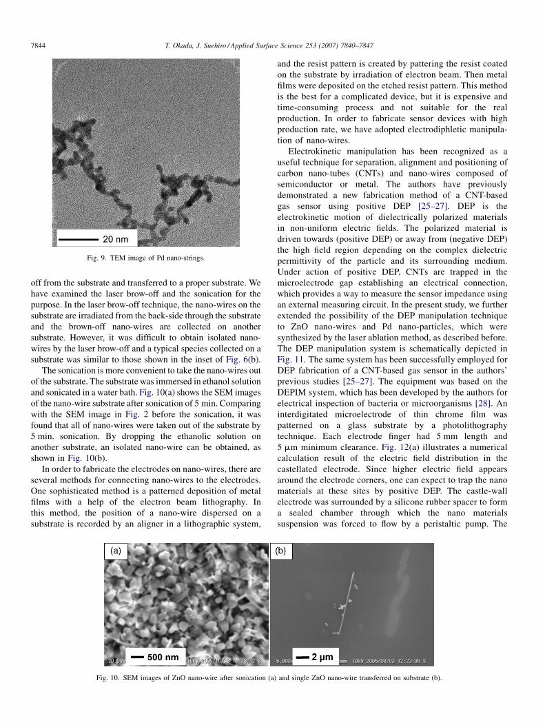
Fig. 9. TEM image of Pd nano-strings.
T. Okada, J. Suehiro / Applied Surface Science 253 (2007) 7840–78477844
off from the substrate and transferred to a proper substrate. We
have examined the laser brow-off and the sonication for the
purpose. In the laser brow-off technique, the nano-wires on the
substrate are irradiated from the back-side through the substrate
and the brown-off nano-wires are collected on another
substrate. However, it was difficult to obtain isolated nano-
wires by the laser brow-off and a typical species collected on a
substrate was similar to those shown in the inset of Fig. 6(b).
The sonication is more convenient to take the nano-wires out
of the substrate. The substrate was immersed in ethanol solution
and sonicated in a water bath. Fig. 10(a) shows the SEM images
of the nano-wire substrate after sonication of 5 min. Comparing
with the SEM image in Fig. 2 before the sonication, it was
found that all of nano-wires were taken out of the substrate by
5 min. sonication. By dropping the ethanolic solution on
another substrate, an isolated nano-wire can be obtained, as
shown in Fig. 10(b).
In order to fabricate the electrodes on nano-wires, there are
several methods for connecting nano-wires to the electrodes.
One sophisticated method is a patterned deposition of metal
films with a help of the electron beam lithography. In
this method, the position of a nano-wire dispersed on a
substrate is recorded by an aligner in a lithographic system,
Fig. 10. SEM images of ZnO nano-wire after sonication (a)
and the resist pattern is created by pattering the resist coated
on the substrate by irradiation of electron beam. Then metal
films were deposited on the etched resist pattern. This method
is the best for a complicated device, but it is expensive and
time-consuming process and not suitable for the real
production. In order to fabricate sensor devices with high
production rate, we have adopted electrodiphletic manipula-
tion of nano-wires.
Electrokinetic manipulation has been recognized as a
useful technique for separation, alignment and positioning of
carbon nano-tubes (CNTs) and nano-wires composed of
semiconductor or metal. The authors have previously
demonstrated a new fabrication method of a CNT-based
gas sensor using positive DEP [25–27]. DEP is the
electrokinetic motion of dielectrically polarized materials
in non-uniform electric fields. The polarized material is
driven towards (positive DEP) or away from (negative DEP)
the high field region depending on the complex dielectric
permittivity of the particle and its surrounding medium.
Under action of positive DEP, CNTs are trapped in the
microelectrode gap establishing an electrical connection,
which provides a way to measure the sensor impedance using
an external measuring circuit. In the present study, we further
extended the possibility of the DEP manipulation technique
to ZnO nano-wires and Pd nano-particles, which were
synthesized by the laser ablation method, as described before.
The DEP manipulation system is schematically depicted in
Fig. 11. The same system has been successfully employed for
DEP fabrication of a CNT-based gas sensor in the authors’
previous studies [25–27]. The equipment was based on the
DEPIM system, which has been developed by the authors for
electrical inspection of bacteria or microorganisms [28]. An
interdigitated microelectrode of thin chrome film was
patterned on a glass substrate by a photolithography
technique. Each electrode finger had 5 mm length and
5 mm minimum clearance. Fig. 12(a) illustrates a numerical
calculation result of the electric field distribution in the
castellated electrode. Since higher electric field appears
around the electrode corners, one can expect to trap the nano
materials at these sites by positive DEP. The castle-wall
electrode was surrounded by a silicone rubber spacer to form
a sealed chamber through which the nano materials
suspension was forced to flow by a peristaltic pump. The
and single ZnO nano-wire transferred on substrate (b).

Fig. 11. Schematic diagram of the experimental set-up for ZnO nano-wire
photosensor fabrication using positive DEP.
T. Okada, J. Suehiro / Applied Surface Science 253 (2007) 7840–7847 7845
ZnO nano-wires were suspended in ethanol, whereas Pd
nano-particles were suspended in deionized water. The DEP
trapping of the nano materials to the microelectrode was
performed with an ac voltage of 100 kHz frequency and 20 V
amplitude (peak to peak value). This ac voltage was also
used to simultaneously measure the electrode impedance by
using a lock-in amplifier controlled by a PC. After 60 min, the
DEP process was stopped and the ethanol was gently
evaporated at room temperature. The thus prepared micro-
electrode retaining the nano materials was observed using a
Fig. 12. (a) Calculation result of the electric field distribution in castellated
microelectrode gaps (FEMLAB). (b) SEM images of ZnO nano-wires trapped
in castellated microelectrode gaps by positive DEP.
scanning electron microscope and tested as a UV photosensor
or a hydrogen gas sensor.
The SEM images of the ZnO nano-wires trapped onto the
castellated microelectrode are shown in Fig. 12(b). The ZnO
nano-wires were trapped around the electrode corner, where the
electric field became higher as theoretically predicted (see
Fig. 12(a)). This implies that the ZnO nano-wires were trapped
under action of positive DEP. The trapped ZnO nano-wires
were aligned along the electric field line and bridged the
electrode gap. The DEP trapping process was little influenced
by the field frequency in the range 1 kHz–1 MHz. The SEM
images also revealed that DEP-trapped ZnO nano-wires could
be firmly immobilized on the microelectrode even after ethanol
evaporation. The impedance measurement revealed that both
the conductance and capacitance components increased with
elapsed time, namely, with more ZnO nano-wires trapped onto
the electrode. The impedance change implies that ZnO nano-
wires establish an electrical connection between the micro-
electrode, which has implications for nano-device self-
assembly using positive DEP. Similar results were obtained
for Pd nano-particles.
4. Device performance
4.1. Photoresponse of the DEP-trapped ZnO nano-wires
Considering the bandgap of ZnO (3.37 eV), it is expected
that the trapped ZnO nano-wires respond to UV light of
wavelength shorter than 380 nm. According to this prediction,
characterization of the DEP-fabricated ZnO nano-wire photo-
sensor was conducted mainly at 365 nm. When the ZnO nano-
wire photosensor was illuminated by 365 nm UV light, the
conductance exponentially increased with a time constant of a
few minutes and then gradually saturated as shown in Fig. 13.
When the UV light was turned off, the conductance
exponentially decreased back to the initial value. At higher
UV intensity, the conductance response became larger. The
Fig. 13. Transient conductance responses of the DEP-fabricated ZnO nano-
wire photosensor to 365 nm UV of various intensities.

T. Okada, J. Suehiro / Applied Surface Science 253 (2007) 7840–78477846
ZnO nano-wire photosensor could detect UV down to the
10 nW/cm2 range. Similar slow UV responses have been
reported for ZnO thin films fabricated by various methods [29].
It has been widely accepted that the slow response could be
attributed to adsorption and UV-triggered photodesorption of
ambient gas molecules such as O2 or H2O. Since the present
experiments were conducted in open air, the slow UV response
of ZnO nano-wires also seemed to be governed by the same
mechanism. According to this mechanism, the conduction
increase of the ZnO nano-wire photosensor is triggered by UV
light-induced photodesorption of the ambient gas. This can be
confirmed from Fig. 14, which shows the spectral response of
the ZnO nano-wire photosensor. The sharp cut-off near 390 nm
agrees with the critical wavelength predicted from the ZnO
bandgap.
Although the UV response mechanism of the DEP-
fabricated ZnO nano-wire photosensor was basically same as
that of ZnO thin film, the DEP-fabricated ZnO nano-wire
photosensor had a considerably higher UV sensitivity than ZnO
thin films as well as ZnO nano-wires assembled between metal
electrodes by other methods. For example, Sharma et al.
investigated the UV response of ZnO thin films prepared by
magnetron sputtering down to 0.6 mW/cm2 intensity at 365 nm
[29]. Photoresponse of ZnO nano-wires was measured using
UV light of 0.3 mW/cm2 intensity [30]. Since the minimum
detection limit of UV intensity was not clearly mentioned in
these literatures, precise comparison of UV detection limit was
difficult. However, the DEP-fabricated ZnO nano-wire photo-
sensor could detect UV light with an intensity as low as 10 nW/
cm2, which has not been detected by using conventional ZnO
photosensors. The possible reason for such a high sensitivity
may be explained as follows. First, the large surface area to
volume ratio of a ZnO nano-wire can enhance UV light
absorption. As shown in Fig. 12(b), DEP-trapped ZnO nano-
wires lie on the surface of the electrode substrate. This
geometry allows the ZnO nano-wire surface to be fully exposed
to the incident light when the photosensor is placed so that the
electrode plane is normal to the light beam. Another advantage
Fig. 14. Spectral response of the DEP-fabricated ZnO nano-wire photosensor
measured at an identical intensity.
is obtained by the DEP fabrication technique demonstrated in
the present study. The authors have previously shown that the
DEP manipulation could realize controlled fabrication of a
CNT-based gas sensor [26]. Although the normalized sensor
response was not dependent on the number of CNTs, the
absolute sensor response DG increased linearly with the sensor
initial conductance G0 or the number of trapped CNTs, which
formed parallel connections on the microelectrode. This
realized a higher signal-to-noise ratio in the gas sensing and
improved the effective sensitivity. Similarly to this, the
photoresponse of the DEP-fabricated ZnO nano-wire photo-
sensor can be regarded as a sum of each nano-wire response.
Considering the number of the electrode gap (DEP sites) on the
sensor electrode (about 2000), the absolute response of the
DEP-fabricated ZnO nano-wire photosensor can be increased
by four orders of magnitude if several nano-wires are trapped in
each gap as shown in Fig. 12(b). By optimizing the electrode
configuration, more nano-wires will be assembled onto one
electrode chip, further increasing the photoresponse.
4.2. Hydrogen gas sensing using DEP-trapped Pd nano-
particles
Pd has been widely used in hydrogen gas sensors because of
the catalytic properties and high hydrogen absorption capacity.
Pd nano-particles are expected to enhance these advantages
because of the large surface area to volume ratio. For example,
Walter et al. demonstrated arrays of mesoscopic Pd wires could
form the basis for hydrogen sensors and hydrogen-actuated
switches [15]. These devices were constructed by electro-
depositing Pd mesowires on a highly oriented pyrolytic
graphite surface and then transferring these mesowires to a
cyanoacrylate film. After an exposure to hydrogen, Pd lattice
expands so that nano-scopic gaps in each mesowire close
decreasing the sensor resistance. It was expected that Pd nano-
particles trapped onto a microelectrode by positive DEP might
Fig. 15. Transient conductance responses of the DEP-fabricated Pd nano-
particle gas sensor to hydrogen gas (1% in dry air). The measurement was
conducted at room temperature.

T. Okada, J. Suehiro / Applied Surface Science 253 (2007) 7840–7847 7847
also serve as a hydrogen sensor according to a similar
mechanism. Fig. 15 shows the conductance response of a DEP-
trapped Pd nano-particle array after an exposure to hydrogen
(1% in dry air) at room temperature. The conductance abruptly
increased at hydrogen exposure with a response time of a few
seconds. The result implies that the DEP-trapped Pd nano-
particle array is potentially applicable to a hydrogen sensor
with a fast response time. At the moment, however, the gas
sensor operation is not reversible, that is, the conductance does
not recover to the initial value when it is purged with pure air.
More detail investigation are under way to improve the sensor
response as well as to understand the hydrogen sensing
mechanism.
5. Conclusion
We successfully synthesized ZnO nano-wires and other
nano-structured ZnO crystals by the nano-particle assisted
deposition (NPAD) with a help of laser ablation in a high
pressure Ar gas. In NPAD, nano-particles were generated in situ
by laser ablation, and they are transported onto a substrate for
the crystal growth. It is thought that a lower melting
temperature of nano-particles which is lower than the melting
temperature of grown nano-structured crystal, plays an
important role in the crystal growth. Pd nano-particles have
been generated by laser-ablation of Pd metal disk in pure water.
Pd nano-particles with a diameter in the range from 3 to 10 nm
and Pd nano-strings have been obtained. These nano-structured
materials were used to fabricate sensor devices, where the
electrodiphletic manipulation was successfully used to collect
the nano-materials onto the electrodes. In the case of the
ultraviolet photosensor made by ZnO nano-wire, a detection
sensitivity of 10 nW/cm2 was achieved and in the case of
hydrogen sensing, the response time of less than 10 s has been
demonstrated with Pd nano-particles.
Acknowledgements
The authors would like to thank Prof. M. Shiratani and Dr. K.
Koga for TEM observation, and Dr. K. Imasaka, Messrs M.
Higashihata, J. Nishimura, K. Kawashima, N. Nakagawa, S.
Hidaka, S. Yamane for their help in performing the experiments.
A part of this work was supported by Grant-in-Aid for Scientific
Research from the Japan Society of Promotion of Sciences (no.
18360151 and no. 18360200).
References
[1] Y.W. Heo, D.P. Norton, L.C. Tien, Y. Kwon, B.S. Kang, F. Ren, S.J.
Pearton, J.R. LaRoche, Mater. Sci. Eng. R 47 (2004) 1.
[2] L.E. Greene, M. Law, D.H. Tan, M. Montano, J. Goldberger, G. Somorjai,
P. Yang, Nano Lett. 5 (2005) 1231.
[3] Y. Zhang, H. Jia, D. Yu, J. Phys. D 37 (2004) 413.
[4] Z.L. Wang, X.Y. Kong, Y. Ding, P. Gao, W.L. Hughes, R. Yang, Y. Zhang,
Adv. Funct. Mater. 14 (2004) 943.
[5] Y. Li, G.W. Meng, L.D. Zhang, F. Phillipp, Appl. Phys. Lett. 76 (2000)
2011.
[6] J.-J. W, S.-C. Liu, Adv. Mater. 14 (2002) 215.
[7] A.B. Hartanto, X. Ning, Y. Nakata, T. Okada, Appl. Phys. A 78 (2004) 299.
[8] T. Okada, B.H. Agung, Y. Nakata, Appl. Phys. A 79 (2004) 1417.
[9] L. Luo, Y. Zhang, S.S. Mao, L. Lin, Sens. Actuators A 126 (2006) 201.
[10] Q. Wan, Q.H. Li, Y.J. Chen, T.H. Wang, X.L. He, J.P. Li, C.L. Lin, Appl.
Phys. Lett. 84 (2004) 3654.
[11] Q.H. Li, Y.X. Liang, Q. Wan, T.H. Wang, Appl. Phys. Lett. 85 (2004)
6389.
[12] C.S. Rout, S.H. Krishna, S.R.C. Vivekchand, A. Govindaraj, C.N.R. Rao,
Chem. Phys. Lett. 418 (2005) 582.
[13] B.S. Kang, F. Ren, Y.W. Heo, L.C. Tien, D.P. Norton, S.J. Pearton, Appl.
Phys. Lett. 86 (2005) 112105.
[14] J. Suehiro1, N. Nakagawa, S. Hidaka, M. Ueda, K. Imasaka, M. Higa-
shihata, T. Okada, M. Hara, Nanotechnology 17 (2006) 2567.
[15] E.C. Walter, F. Favier, R.M. Penner, Anal. Chem. 74 (2002) 1546.
[16] J. Chen, B. Wiley, J. McLellan, Y. Xiong, Z.-Y. Li, Y. Xia, Nano Lett. 5
(2005) 2058.
[17] A. Henglein, J. Phys. Chem. 97 (1993) 5457.
[18] M. Prochazka, P. Mojzes, J. Stepanek, B. Vlckova, P.-Y. Turpin, Anal.
Chem. 69 (1997) 5103.
[19] T. Tsuji, K. Iryo, H. Ohta, Y. Nishimura, Jpn. J. Appl. Phys. 39 (2000) 981.
[20] H.T. Wang, B.S. Kang, F. Ren, L.C. Tien, P.W. Sadik, D.P. Norton, S.J.
Pearton, J. Lin, Appl. Phys. A 81 (2005) 1117.
[21] J. Sehiro, G. Zhou, M. Hara, J. Phys. D 36 (2003) L109.
[22] T. Okada, K. Kawashima, Y. Nakata, Thin Solid Films 506–507 (2006)
274.
[23] J.C. Johnson, H. Yan, R.D. Schaller, L.H. Haber, R.J. Saykally, P. Yang, J.
Phys. Chem. B 105 (2001) 11387.
[24] T. Okada, K. Kawashima, M. Ueda, Appl. Phys. A 81 (2005) 907.
[25] J. Suehiro, G. Zhou, M. Hara, J. Phys. D Appl. Phys. 36 (2003) L109.
[26] J. Suehiro, G. Zhou, H. Imakiire, W. Ding, M. Hara, Sens. Actuators B 108
(2005) 398.
[27] J. Suehiro, H. Imakiire, S. Hidaka, W. Ding, G. Zhou, K. Imasaka, M.
Hara, Sens. Actuators B 114 (2006) 943.
[28] J. Suehiro, R. Yatsunami, R. Hamada, M. Hara, J. Phys. D 32 (1999) 2814.
[29] P. Sharma, K. Sreenivas, K.V. Rao, J. Appl. Phys. 93 (2003) 3963.
[30] H. Kind, H. Yan, B. Messer, M. Law, P. Yang, Adv. Mater. 14 (2002) 158.