system level analysis of fast, per-core dvfs using on-chip ...dbrooks/kim2008_hpca.pdf · system...
TRANSCRIPT
System Level Analysis of Fast, Per-Core DVFSusing On-Chip Switching Regulators
Wonyoung Kim, Meeta S. Gupta, Gu-Yeon Wei and David Brooks
School of Engineering and Applied Sciences, Harvard University, 33 Oxford St., Cambridge, MA 02138
{wonyoung,meeta,guyeon,dbrooks}@eecs.harvard.edu
Abstract
Portable, embedded systems place ever-increasing demands on
high-performance, low-power microprocessor design. Dynamic
voltage and frequency scaling (DVFS) is a well-known technique
to reduce energy in digital systems, but the effectiveness of DVFS
is hampered by slow voltage transitions that occur on the order of
tens of microseconds. In addition, the recent trend towards chip-
multiprocessors (CMP) executing multi-threaded workloads with
heterogeneous behavior motivates the need for per-core DVFS
control mechanisms. Voltage regulators that are integrated onto
the same chip as the microprocessor core provide the benefit of
both nanosecond-scale voltage switching and per-core voltage
control. We show that these characteristics provide significant
energy-saving opportunities compared to traditional off-chip regu-
lators. However, the implementation of on-chip regulators presents
many challenges including regulator efficiency and output voltage
transient characteristics, which are significantly impacted by the
system-level application of the regulator. In this paper, we describe
and model these costs, and perform a comprehensive analysis of a
CMP system with on-chip integrated regulators. We conclude that
on-chip regulators can significantly improve DVFS effectiveness
and lead to overall system energy savings in a CMP, but architects
must carefully account for overheads and costs when designing
next-generation DVFS systems and algorithms.
1. Introduction
Dynamic voltage and frequency scaling (DVFS) was introduced in
the 90’s [19], offering great promise to dramatically reduce power
consumption in large digital systems by adapting both voltage and
frequency of the system with respect to changing workloads [16,28,
30,36]. Unfortunately, the full promise of DVFS has been hindered
by slow off-chip voltage regulators that lack the ability to adjust
to different voltages at small time scales. Modern implementations
are limited to temporally coarse-grained adjustments governed by
runtime software (i.e. the operating system) [1,31]. In recent years,
researchers have turned to chip multiprocessor architectures as a
way of maintaining performance scaling while staying within tight
power constraints. There are several examples of processors that
use a large number of simple tiles, demonstrating a trend towards
many-core designs [6, 22, 26]. This trend, coupled with diverse
workloads found in modern systems, motivates the need for fast,
per-core DVFS control.
Voltage regulators are found in nearly all computing systems
and are essential for delivering power from an energy source (e.g.,
battery) to multiple integrated circuits (e.g., microprocessor) at
their respective, desired fixed or time-varying voltage levels. In or-
der to achieve high energy-conversion efficiencies, inductor-based
switching voltage regulators are commonly used. Conventional
switching regulators operate at relatively low switching frequen-
cies (< 5MHz) and utilize bulky filter components (i.e. discrete
inductors and capacitors) [21, 23, 37, 39]. Hence, voltage regula-
tor modules (VRM) typically are separate, board-level components
that, unfortunately, have slow voltage adjustment capabilities—
limited to tens of microsecond timescales. The cost and bulk of
these modules also preclude using these efficient regulators to im-
plement multiple on-chip power domains.
In recent years, there has been a surge of interest to build on-
chip integrated switching voltage regulators [5, 14, 27, 34]. These
regulators offer the potential to provide multiple on-chip power do-
mains in future CMP systems. An on-chip regulator, operating with
high switching frequencies, can obviate bulky filter components
(the filter inductor and capacitor), allow the filter capacitor to be
integrated entirely on the chip, place smaller inductors on the pack-
age, and enable fast voltage transitions at nanosecond timescales.
Moreover, an on-chip regulator can easily be divided into multi-
ple parallel copies with little additional overhead, readily provid-
ing multiple on-chip power domains. Unfortunately, these poten-
tial benefits are tempered by lower energy-conversion efficiencies
resulting from high switching frequencies and increased suscepti-
bility to load current steps.
This paper explores the interplay of the promising character-
istics and costs of employing on-chip regulator designs in mod-
ern CMP system architectures. While this study considers CMP
designs comprising multiple low-power processor cores within
the context of a mobile embedded system, the analysis described
throughout this paper can be extended to higher-power processors
as well.
Figure 1 illustrates three power-supply configurations that this
paper studies. The first configuration (left) represents a conven-
tional design scenario that only uses an off-chip voltage regula-
tor. This voltage regulator directly steps the power supply voltage,
assumed to be 3.7V provided by a Li-Ion battery, down to a pro-
cessor voltage ranging from 0.6V to 1V. The second configuration
(middle) implements a two-step voltage conversion scenario. Given
an inherent degradation in conversion efficiencies for large step-
down ratios, an off-chip regulator performs the initial step-down
from 3.7V to 1.8V, which can be shared by other on-board com-
ponents. The 1.8V supply then drives an on-chip voltage regulator
that further steps the voltage down to a range of 0.6V to 1V as a
single power supply domain distributed across a 4-core CMP. The
third configuration (right) expands on the second configuration by
providing four separate on-chip power domains via individual on-
chip voltage regulators. These three configurations constitute the
framework through which we compare the costs and benefits of
fast, per-core DVFS enabled by on-chip regulators.

No On-Chip
Regulator
One On-Chip Regulator
with Global DVFS
Four On-Chip Regulators
with per-Core DVFS
Processor
On-Chip Regulators
Processor
On-Chip Regulator
1.8V
Processor
3.7V
Off-Chip
Regulator
Power
Supply
Core 0
0.6V-1V
0.6V-1V
V0
V1
V2
V3
3.7V
Off-Chip
Regulator
Power
Supply
1.8V
3.7V
Off-Chip
Regulator
Power
Supply
Core 1
Core 2
Core 3
Core 0
Core 1
Core 2
Core 3
Core 0
Core 1
Core 2
Core 3
Figure 1. Three power-supply configurations for a 4-core CMP.
The main contributions of this work are as follows:
1. We explore the energy savings offered by implementing both
temporally fine-grained and per-core DVFS in a 4-core CMP
system using an offline DVFS algorithm (Section 2).
2. We present a detailed on-chip regulator model and design space
analysis that considers key regulator characteristics—DVFS
transition times and overheads, load current transient response,
and regulator losses (Sections 3 and 4).
3. We combine the energy savings with the on-chip regulator cost
models and come to several conclusions. For a single power
domain, on-chip regulator losses offset the gains from fast
DVFS for many workloads. In contrast, fast, per-core DVFS
can achieve energy savings (>20%) when compared to conven-
tional, single power domain, off-chip regulators with compara-
tively slow DVFS (Section 5).
2. Potential of Fast and Per-Core DVFS schemes
Dynamic voltage and frequency scaling can be an effective tech-
nique to reduce power consumption in processors. DVFS con-
trol algorithms can be implemented at different levels, such as in
the processor microarchitecture [20], the operating system sched-
uler [17], or through compiler algorithms [15, 38]. Most previous
work in the domain of DVFS control algorithms focus on coarse
temporal granularity, e.g., voltage changes on the order of several
microseconds, which is appropriate given slow response times of
off-chip regulators. In contrast, on-chip regulators offer much faster
voltage transitions as presented in Figure 2. This figure, a simula-
tion of the on-chip regulator model described in a later section,
shows voltage transitions can occur on the order of tens of nanosec-
onds, several orders of magnitude faster than off-chip regulators.
DVFS algorithms implemented at the microarchitecture level pro-
vide the finest level of temporal control, hence, are good candidates
for the fine-grained approach that we consider. In this section, we
explore the benefits of fast DVFS with fine temporal resolution and
also highlight the benefits of per-core voltage domains compared to
chip-wide DVFS. To explore the benefits and tradeoffs associated
with temporally fine-grained and per-core DVFS, we rely on an of-
fline DVFS algorithm that can easily be applied across the wide
range of DVFS transition times we consider. Section 2.1 provides a
brief overview of the simulation framework used in our study, and
the methodology of the offline DVFS algorithm is described in Sec-
tion 2.2. We then discuss the effects of finer temporal granularity
(Section 2.3), and the savings for per-core versus chip-wide DVFS
schemes (Section 2.4).
Output Voltage (V)
1.1
1
0.9
0.8
0.7
0.6
0.5
1000 200 300 400 500 600 700 800 900
Time (ns)
1V, 1GHz
0.6V, 0.6GHz
0.866V, 0.866GHz
0.733V, 0.733GHz
1V, 1GHz
Figure 2. DVFS transition times with an on-chip regulator
Frequency
Core Area
Branch
Penalty
Int registers
IL1
ITLB entries
MSHR sizeL2 size
1GHz @ 65nm
16mm2
7 cycles
Hybrid Branch Predictor
32
32KB, 32-way, 32B block
Hi/Miss latency 2/1 cycles
Fetch/Issue/Retire
Vdd
FP registers
Branch Predictor
32KB, 32-way, 32B block
Hi/Miss latency 2/1 cycles
MESI-protocol
BTB (1K entries)
RAS (32 entries)
32
DL1
DTLB entries
Write Buffer size
128
16MSHR size
64
8
512 KB 16
1 V
2/2/2
Table 1. Processor configuration and system parameters for SESC.
2.1 Simulation Framework
We employ an architectural power-performance simulator that gen-
erates realistic current traces. We use SESC [25], a multi-core
simulator, integrated with power-models based on Wattch [7],
Cacti [29], and Orion [32]. A simple in-order processor model
represents configurations similar to embedded processors like Xs-
cale [10]. The per-core current load is 400mA when fully active
and 120mA when idle. We model a configuration with a shared-L2
configuration, private-L1 caches in each processor, and a MESI-
based coherence protocol. Table 1 lists the details of the 4-core
processor configuration and system parameters. The simulator was
modified to obtain cycle-by-cycle current profiles for each core in
the system.
In a CMP-based system, it is important to understand the in-
teractions between the multiple cores. These interactions can be
accurately characterized by analyzing a mix of multi-threaded and
multi-programmed benchmarks. We use a composite benchmark
suite composed of applications from SPEC2K, ALPBench [18],
and SPLASH2 [35]. For multi-programmed scenarios, we consider
several mixtures of a memory-bound benchmark (mcf) and a cpu-
bound benchmark (applu) from SPEC2K. Table 2 lists the different
benchmarks used in this study along with the ratio of memory cy-
cles to total runtime of the application for each. All benchmarks are
run for 400M instructions after fast forwarding through the initial-
ization phase.
2.2 Offline DVFS Algorithm
The goal of any DVFS algorithm is to minimize energy consump-
tion of the application within certain performance constraints. This
can be done by exploiting the slack due to asynchronous mem-
ory events. Scaling down the frequency of the processor slows
down cpu-bound operations, but does not affect the time taken
by memory-bound operations. We exploit the presence of such
memory-bound intervals to reduce the voltage and frequency of the
processor. The effectiveness of such a DVFS scheme is directly re-
lated to the ratio of memory-bound cycles to cpu-bound cycles.

applu4
3-high memory-bound (mcf) and 1-high cpu-bound (applu)
mcf1, applu3
mcf2, applu2
mcf3, applu1
mcf4
raytrace
cholesky
facerec
fft
ocean-con
1-high memory-bound (mcf) and 3-high cpu-bound (applu)
2-high memory-bound (mcf) and 2-high cpu-bound (applu)
4-high cpu-bound (applu)
4-high memory-bound (mcf)
Tachyon Ray Tracer
Cholesky Factorization
CSU Face Recognizer
Fast Fourier Transform
Large Scale Ocean Simulation
Benchmarks DescriptionMemory Cycles
Total Runtime
0.697 (mcf)
and
0.051 (applu)
0.697
0.051
0.058
0.197
0.22
0.4
0.47
Table 2. Benchmark Suite.
As this paper aims to study the potential system-wide benefits
of using on-chip voltage regulators, the offline algorithm is applied
to all configurations and it optimizes DVFS settings based on a
global view of workload characteristics. We formulate the DVFS
control problem as an integer linear programming (ILP) optimiza-
tion problem, which seeks to reduce the total power consumption
of the processor within specific performance constraints (δ). This
approach is similar to the one proposed in [38]. We divide the appli-
cation runtime into N intervals based on different temporal gran-
ularities of DVFS. A total of L = 4 voltage/frequency (V/F) levels
are considered. For each runtime interval i and frequency j, the
power consumption, Pij , is calculated. The delay for each inter-
val and V/F level, Dij , is also calculated. Heuristics for the de-
lay of individual intervals are obtained by calculating the relative
memory-boundness of each interval through cache miss behavior.
Equations 1- 3 specify the ILP formulation of our offline algorithm.
The overheads associated with switching between different volt-
age/frequencies settings are not considered in the optimization, but
are included later in Section 4.
min(
N∑
i=1
L∑
j=1
Pijxij) (1)
(
N∑
i=1
L∑
j=1
Dijxij) < δ (2)
N∑
i=1
L∑
j=1
xij = N (3)
We consider an in-order processor with the capability of switch-
ing between four voltage settings: 1V, 0.866V, 0.733V, and 0.6V,
with proportionally scaled frequencies from 1GHz down to 600MHz.
As in Xscale [10], we assume the processor can operate through
voltage transitions by quickly ramping down frequency before the
voltage ramps down. Conversely, we ramp up the voltage and only
switch the frequency after the voltage has settled to higher levels.
Clock synthesis that combines finely-spaced edges out of a delay-
locked loop can provide rapid frequency adjustment without PLL
re-lock penalties [11].
The offline algorithm finds voltage/frequency settings at each
interval to minimize power while maintaining a specified perfor-
mance constraint. In this study, we consider performance con-
straints of 1%, 5%, 10%, 15%, and 20%. In order to keep the
runtime overheads of the ILP algorithm tractable, we divide the
simulation trace into smaller windows of 2M cycles each; finding
optimal DVFS assignments within the windows, but not necessar-
ily across the entire trace. The overall power savings presented in
this paper represents the average power savings across all 2M-cycle
windows for each application.
1 1.05 1.1 1.15 1.20.2
0.4
0.6
0.8
1
Relative Delay
Re
lati
ve
Po
we
r
static
100us
10us
1us
200ns
100ns
(a) mcf
1 1.05 1.1 1.15 1.20.2
0.4
0.6
0.8
1
Relative Delay
Re
lati
ve
Po
we
r
static
100us
10us
1us
200ns
100ns
(b) fft
Figure 3. Benefits of fine-grained DVFS scheme for mcf and fft.
2.3 Effects of Finer Temporal Resolution
On-chip regulators allow voltage transitions to occur at a rate of
tens of nanoseconds as compared to microseconds for off-chip
regulators. The fast voltage-scaling capability of on-chip regula-
tors provides the potential for applying DVFS at very fine-grained
timescales. A fine-grained DVFS scheme can more closely track
different cpu- and memory-bound phases than a coarse-grained
scheme and, hence, reduce power consumption without perfor-
mance degradation. However, the power-saving benefits of a fine-
grained technique depend on the distribution of memory misses in
the benchmark.
Figure 3(a) shows the impact of scaling temporal DVFS resolu-
tions for mcf and fft. Resolutions in the range of 10-100µs represent
the coarse-grained DVFS schemes and 100-200ns represent fine-
grained, on-chip DVFS. We also consider a static voltage/frequency
scaling scheme (representative of coarse-grained OS-level control)
that fixes DVFS settings at one point for the entire benchmark for
each performance target. In some cases, the ILP algorithm fails
to match the performance constraint and data points may deviate
from initial performance targets. As discussed previously, mcf is
a memory-bound benchmark, with approximately 70% of its run-
time spent servicing memory misses. The fine-grained approach
can capture these memory-miss intervals and achieve as much as
60% power savings for only 5% performance degradation. In con-
trast, coarse-resolution windows fail to capture all of these inter-
vals, achieving less power savings for the same performance con-
straint (between 35-40% savings for the same 5% performance
loss). In general,we find that the benefits of fast DVFS depends
heavily on the application. For example, fine-grained DVFS is not
much better than the coarse-grained schemes for fft (Figure 3(b)),
but show an 8% power benefit compared to static voltage/frequency
scaling.
2.4 Per-Core vs. Chip-Wide DVFS
Chip multiprocessor systems running heterogeneous workloads
add the dimension of benefiting from per-core DVFS. Isci et al.
show multiple power domains offer power savings in CMP sys-
tems over a single power domain [16]. However, due to cost and
system board area constraints, it may not be practical to implement
multiple power domains using off-chip voltage regulators. On the
other hand, on-chip regulators can easily be modified to accommo-
date multiple power-domains with little additional cost (explained
in Section 4). We refer to chip-wide DVFS as a global setting for
voltage/frequency of the entire chip based on the activity of the
whole chip, as opposed to each core. In this section we compare
per-core and chip-wide DVFS schemes with 100ns transition times
for both multi-threaded and multi-programmed workloads.
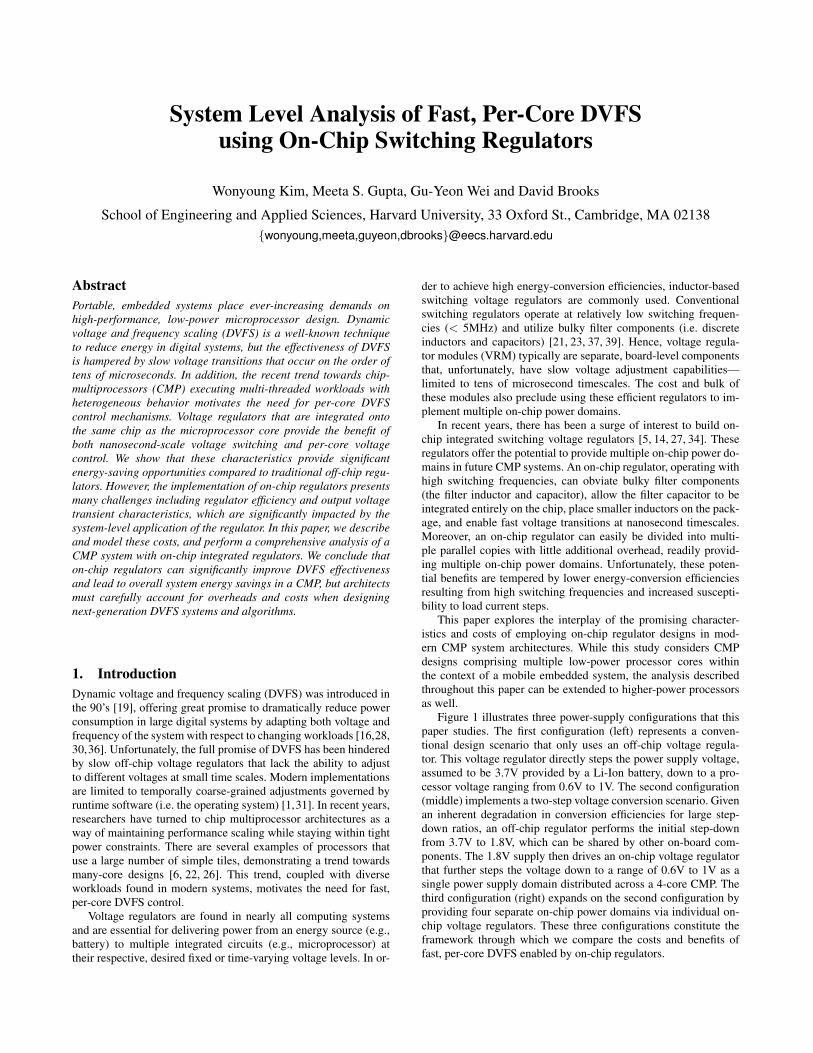
Figure 4 plots the relative power savings for per-core DVFS and
chip-wide DVFS schemes across a range of multi-threaded bench-
1 1.05 1.1 1.15 1.2
0.4
0.6
0.8
1
Relative Delay
Re
lati
ve
Po
we
r
raytracecholeskyfacerecfftocean
(a) Chip-Wide DVFS
1 1.05 1.1 1.15 1.2
0.4
0.6
0.8
1
Relative Delay
Re
lati
ve
Po
we
r
raytracecholeskyfacerecfftocean
(b) Per-Core DVFS
Figure 4. Per-Core DVFS for multi-threaded applications.
Core 0
Core 1
Core 2
Core 3
Total
Cycle0 500 1000 1500 2000
1
Activity
1
0
1
0
1
0
1
0
0
(a) Activity profile of ocean
Core 0
Core 1
Core 2
Core 3
10.80.6
10.80.6
10.80.6
10.80.6
10.80.6
Cycle
Frequency (GHz)
0 500 1000 1500 2000
(b) Frequency settings
Figure 5. Snapshot of ocean with per-core and chip-wide DVFS.
Core 0
Core 1
Core 2
Core 3
1
Cycle
Activity
0 200 400 600 800
1 Total
0
1
0
1
0
1
0
0
(a) Activity profile of fft
Core 0
Core 1
Core 2
Core 3
10.80.6
10.80.6
10.80.6
10.80.6
10.80.6
Cycle
Frequency (GHz)
0 200 400 600 800
(b) Frequency settings
Figure 6. Snapshot of fft with per-core and chip-wide DVFS.
marks and a significant difference can be observed for most of the
benchmarks (e.g., ocean, fft, facerec). However, benchmarks like
raytrace yield only slight differences between the two approaches.
This can be attributed to the highly cpu-bound behavior of raytrace,
which offers fewer frequency-scaling opportunities.
Multi-threaded applications can have similar phases (cpu- or
memory-bound) of operation across the cores. Figure 5(a) shows
a snapshot of activity on each core for a four-threaded version of
ocean. We see similar behavior across all four threads, but there
is a slight shift in the activity across the cores. While per-core
DVFS is able to capture DVFS scaling opportunities in the indi-
vidual threads, the time windows where the scaling is applied are
different. Because of this, a chip-wide DVFS scheme, based on
the combined activity of the four threads, finds fewer DVFS scal-
ing opportunities as shown by the global scaling in Figure 5(b). In
contrast, Figure 6(a) presents the activity snapshot for fft. We see
that the activity profiles of core 0 and core 2 are synchronized in
time, as are the activity profiles of core 1 and core 3. This leads
to a more effective chip-wide DVFS schedule, demonstrated by the
1 1.1 1.20.2
0.4
0.6
0.8
1
Relative Delay
Rela
tive P
ow
er
4 cpu
1 mem, 3 cpu
2 mem, 2 cpu
3 mem, 1 cpu
4 mem
(a) Chip-Wide DVFS
1 1.1 1.20.2
0.4
0.6
0.8
1
Relative Delay
Rela
tive P
ow
er
4 cpu
1 mem, 3 cpu
2 mem, 2 cpu
3 mem, 1 cpu
4 mem
(b) Per-Core DVFS
Figure 7. Per-core DVFS for multi-programming scenarios.
global scaling in Figure 6(b). As mentioned in Section 2.2, the of-
fline algorithm relies on a global view of each 2M cycle window
and, hence, the local voltage/frequency assignments for short inter-
vals shown do not necessarily line up with local activities.
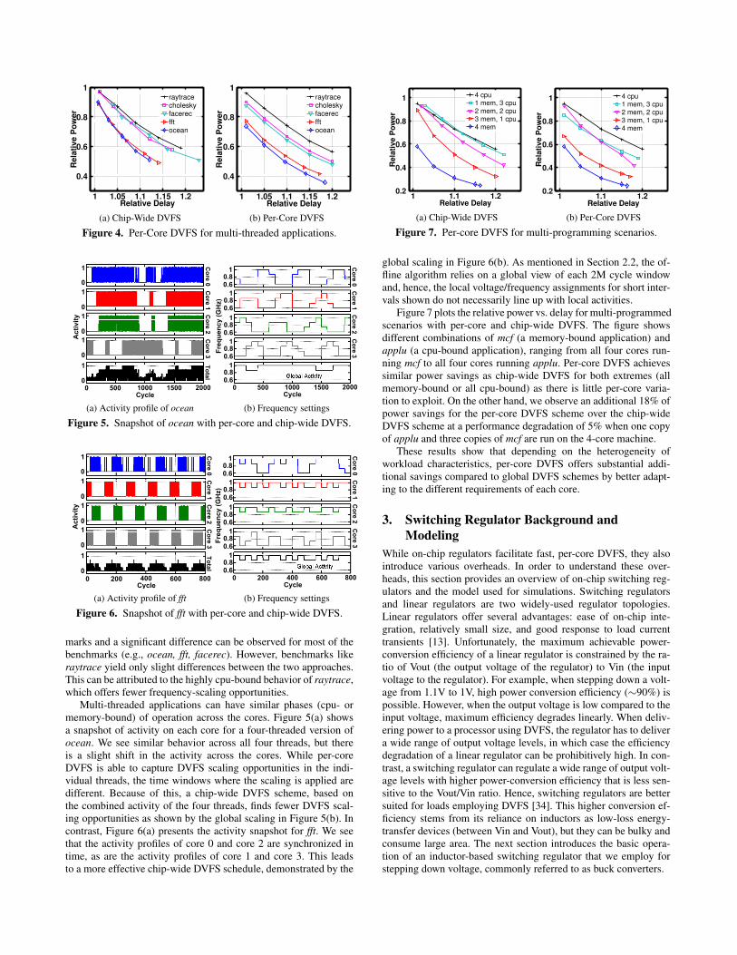
Figure 7 plots the relative power vs. delay for multi-programmed
scenarios with per-core and chip-wide DVFS. The figure shows
different combinations of mcf (a memory-bound application) and
applu (a cpu-bound application), ranging from all four cores run-
ning mcf to all four cores running applu. Per-core DVFS achieves
similar power savings as chip-wide DVFS for both extremes (all
memory-bound or all cpu-bound) as there is little per-core varia-
tion to exploit. On the other hand, we observe an additional 18% of
power savings for the per-core DVFS scheme over the chip-wide
DVFS scheme at a performance degradation of 5% when one copy
of applu and three copies of mcf are run on the 4-core machine.
These results show that depending on the heterogeneity of
workload characteristics, per-core DVFS offers substantial addi-
tional savings compared to global DVFS schemes by better adapt-
ing to the different requirements of each core.
3. Switching Regulator Background and
Modeling
While on-chip regulators facilitate fast, per-core DVFS, they also
introduce various overheads. In order to understand these over-
heads, this section provides an overview of on-chip switching reg-
ulators and the model used for simulations. Switching regulators
and linear regulators are two widely-used regulator topologies.
Linear regulators offer several advantages: ease of on-chip inte-
gration, relatively small size, and good response to load current
transients [13]. Unfortunately, the maximum achievable power-
conversion efficiency of a linear regulator is constrained by the ra-
tio of Vout (the output voltage of the regulator) to Vin (the input
voltage to the regulator). For example, when stepping down a volt-
age from 1.1V to 1V, high power conversion efficiency (∼90%) is
possible. However, when the output voltage is low compared to the
input voltage, maximum efficiency degrades linearly. When deliv-
ering power to a processor using DVFS, the regulator has to deliver
a wide range of output voltage levels, in which case the efficiency
degradation of a linear regulator can be prohibitively high. In con-
trast, a switching regulator can regulate a wide range of output volt-
age levels with higher power-conversion efficiency that is less sen-
sitive to the Vout/Vin ratio. Hence, switching regulators are better
suited for loads employing DVFS [34]. This higher conversion ef-
ficiency stems from its reliance on inductors as low-loss energy-
transfer devices (between Vin and Vout), but they can be bulky and
consume large area. The next section introduces the basic opera-
tion of an inductor-based switching regulator that we employ for
stepping down voltage, commonly referred to as buck converters.

Control
Vhigh, Vlow
Lout
Cout
DTswitch
DTswitch
Vhys
Vin
Vout
Rfilter Cfilter
Processor
(a) Buck converter with hysteretic control
Average Current to Load
Interleaved Current in each phase
time
CTRL1
CTRL2
CTRLn
Processor
(b) Multiphase buck converter
Figure 8. Buck converter schematics
3.1 Background on Buck Converters
A typical buck regulator, shown in Figure 8(a), is comprised of
three sets of components: switching power transistors, the output
filter inductor (Lout) and capacitor (Cout), and the feedback con-
trol consisting of a hysteretic comparator and associated filter ele-
ments (Cfilter and Rfilter) that enhance loop stability. The power
transistors can simply be viewed as an inverter that switches on
and off at a switching frequency and provides a square wave to
the low-pass output filter composed of Lout and Cout. The regula-
tor output, Vout, powers the microprocessor load and its voltage is
approximately set by the duty cycle of the square wave. This reg-
ulated voltage exhibits small ripples since the filter attenuates the
high-frequency square wave. The feedback loop is closed by feed-
ing Vhys, which is the output of the filter composed of Cfilter and
Rfilter , to the hysteretic comparator. The duty cycle of the square-
wave input to the power transistors is set by the hysteretic compara-
tor output. As shown in Figure 8(a), the hysteretic comparator has
a high threshold (Vhigh) and a low threshold voltage (Vlow). The
PMOS power switch turns on when Vhys drops below Vlow, and
the NMOS turns on when the Vhys increases above Vhigh. Since
Vout directly affects Vhys, when Vout fluctuates in response to load
current transients, hysteretic control can react very quickly. While
there are several other feedback control schemes one can employ
for a buck regulator, hysteretic control offers fast transient response
characteristics while keeping design complexity low [21].
The power transistors and inductor shown in Figure 8(b) can be
interleaved to form a multiphase buck converter. Multiphase con-
verters have been proposed for high load current applications [23,
37, 39], since they can reduce the peak current in each inductor.
Multiphase designs are also well-suited for on-chip regulators de-
signs, because they allow for small filter inductor and capacitor
sizes, and can achieve fast transient response. Parallel sets of power
transistors and inductors are interleaved and connected to the same
load such that current through each inductor is interleaved across
even time intervals. Hence these interleaved inductor currents can-
cel out at the output node and result in an average current that has
small ripple. Moreover, this interleaving accommodates the use of
small output filter capacitance while meeting small voltage ripple
constraints. However, more phases come with the overhead of con-
suming more on-die area. Since size of the power transistors scale
with the current provided per phase, the total area of the power
transistors depends on load current specifications and is largely in-
dependent of the number of phases. However, the area occupied by
Cfilter , Rfilter , and the hysteretic comparator increases linearly
with the number of phases.
3.2 Model and Simulation of Buck Regulator
This section describes how the off-chip and on-chip regulators
are modeled and simulated in this work. Figure 9 illustrates the
overall power delivery network of the example embedded system,
from the Li-Ion battery to the processor load, for two regulator
configurations—with and without an on-chip regulator. This is a
more detailed version of Figure 1, adding in the parasitic elements
associated with the power delivery network. This figure shows the
parasitic inductors and resistors along the PCB trace and package,
and decoupling capacitance added to mitigate voltage fluctuations.
This model is derived from the Intel Pentium 4 package model,
but scaled to be consistent with our assumptions of power draw in
embedded processors [12]. The off-chip regulator is modeled as an
ideal voltage source, but losses are accounted for by using power-
conversion efficiencies extracted from published datasheets [4].
The on-chip regulator is modeled in greater detail with para-
sitics. We assume an on-chip regulator using a commercial 65nm
CMOS process. Extensive SPICE simulations were run to extract
parasitic values that can significantly affect regulator efficiency and
performance. These parasitics include feedback control path de-
lays, power MOSFET gate capacitance and on-state resistance, and
on-chip decoupling capacitor losses. The inductors required by the
on-chip regulators are assumed to be air-core surface-mount induc-
tors [2] attached on-package [14, 27]. The inductors are connected
via C4 bumps, which introduce series resistance. The total number
of C4 bumps for power is assumed to be equal for both off-chip and
on-chip regulators for fair comparisons. For the on-chip regulator,
we use 60% of the C4 bumps to connect package-mounted induc-
tors to the die. The remaining bumps are used to connect Vin of
the on-chip regulator to the PCB. Since the off-chip scheme uses
more C4 bumps to connect the processor to the package, it has
lower package-to-chip impedance compared to the on-chip scheme.
Careful modeling of parasitic losses is required to accurately esti-
mate on-chip regulator efficiency, which is found to be consistent
with published results [14, 27].
Transient response characteristics also impact the efficacy of
using on-chip voltage regulators. Hence, we rely on a detailed
Matlab-Simulink model of the on-chip regulator to thoroughly in-
vestigate the regulator’s performance given load current transients
and voltage transition demands of realistic workloads seen in Sec-
tion 2. The model is built using the SimPowerSystems blockset [3]
of Simulink. This Simulink model includes all of the parasitic ele-
ments described above since they also impact transient behavior in
addition to efficiency.

Li-ion
Battery
(3.7V)
Off-Chip
Power
Regulator
3.7V 1V
PCB Package
Package-
to-Chip
Connection Processor
PCB
de-cap
Package
de-cap
Processor
de-cap
Off-Chip On-Chip
(a)
PCB Package
Package-
to-Chip
Connection Processor
PCB
de-cap
Package
de-cap
Processor
de-cap
On-Chip
Power
Regulator
(1.8V 1V)
Off-Chip On-Chip
(b)
Li-ion
Battery
(3.7V)
Off-Chip
Power
Regulator
(3.7V 1.8V)
Figure 9. Power delivery network using (a) only off-chip and (b)
both off-chip and on-chip regulators.
The next section studies the characteristics of on-chip regulators
in more depth with simulation results based on the aforementioned
model. The characteristics are presented in comparison to those for
an off-chip regulator. We also study the tradeoffs associated with
different regulator characteristics in order to minimize overheads.
4. Characteristics of On-Chip Regulators
Voltage regulators are typically off-chip devices [21,23,37,39] due
to the large power transistors and output filter components that
are required. However, this regulator module can occupy a sig-
nificant portion of the PCB area, making it costly to utilize mul-
tiple regulators for per-core DVFS. Recently, on-chip regulators
have been proposed, integrated on the same die as the processor
load [5,14,27,34]. By using much higher switching frequencies, the
bulky off-chip inductors and capacitors can be reduced in size and
moved onto the package and die, respectively. Hence, on-chip reg-
ulators offer an interesting solution that can supply multiple power
domains in CMPs with per-core DVFS.
In addition to reducing size, on-chip regulators are also capable
of fast voltage switching, which again results from higher switch-
ing frequencies. The switching frequency of an off-chip regulator
is typically on the order of hundreds of KHz to single-digit MHz,
whereas on-chip regulator designs push switching frequency above
100MHz. Unfortunately, the higher frequency switching comes at
the cost of degrading the conversion efficiency of on-chip regula-
tors, lower than that of their off-chip counterparts. Hence, there are
tradeoffs between regulator size, voltage switching speed, and con-
version efficiency.
In order to design an on-chip regulator with minimum over-
heads, we study three important regulator characteristics: regula-
tor efficiency, load transient response, and voltage switching time.
Figure 10 summarizes the tradeoffs between these three character-
istics. Each dot represents a regulator design with different parame-
ters: output filter inductor and capacitor sizes, Cfilter , Rfilter , and
switching frequency. Voltage variation is the percentage change of
the output voltage droops during load transients. Regulator loss in-
cludes both switching power and resistive losses associated with
the power transistors in addition to all components of resistive
loss throughout the power delivery network. Different colors (or
shades) of each dot correspond to how quickly the voltage can tran-
sition between 0.6V and 1V. The figure shows that different de-
sign parameters can shift regulator characteristics. Regulators with
higher switching frequencies are capable of fast voltage scaling (i.e.
short scaling times) and exhibit smaller voltage variations, but in-
cur higher regulator loss. Conversely, regulators with lower switch-
0 5 10 15 20 25 30 35 405
10
15
20
25
30
35
40
Voltage Variation (%)
Re
gu
lato
r L
os
s (
%)
Vo
ltag
e S
ca
ling
Tim
e (n
s)
10
15
20
25
30
35
40
45
50
Figure 10. Regulator loss, voltage variation, and voltage scaling
time of a regulator with different parameters.
0.6 0.7 0.8 0.9 1
70
75
80
85
90
Output Voltage (V)
Eff
icie
nc
y (
%)
Activity Factor = 1Activity Factor = 0.5Activity Factor = 0
(a) Efficiency
0.6 0.7 0.8 0.9 150
100
150
200
250
Re
gu
lato
r P
ow
er
(mW
)
Output Voltage (V)
Activity Factor = 1Activity Factor = 0.5Activity Factor = 0
(b) Power
Figure 11. Regulator efficiency and power vs. output voltage for
different activity factors.
ing frequencies have lower regulator loss, but exhibit larger volt-
age variations and slower voltage scaling capabilities. By under-
standing these characteristics, designers can exploit the tradeoffs to
minimize overheads depending on the specific needs and attributes
of the processor load. For example, if the load can leverage fast
DVFS for significant power savings (seen for memory-bound appli-
cations), a regulator that prioritizes minimization of voltage scaling
times may yield the best overall system-level solution. On the other
hand, if the load is steady with small current transients, design pa-
rameters ought to be chosen to minimize regulator loss. To better
understand how one can make appropriate design tradeoffs, the next
subsections delve into the regulator characteristics in greater detail.
4.1 Regulator Efficiency
An ideal regulator delivers power from a power source (e.g., bat-
tery) to the load without any losses. Unfortunately, the regulator it-
self consumes power while delivering power to a load. Conversion
efficiency is an important metric commonly used to evaluate regula-
tor performance. It is the ratio of power delivered to the load by the
regulator to the total power into the regulator. Regulator losses are
dominated by switching power and resistive losses, which depend
on the size of the switching power transistors, switching frequency,
and load conditions (e.g., load current levels). Larger power devices
reduce resistive losses at the expense of higher switching power.
Higher switching frequencies lead to higher switching power, but
can also reduce resistive loss. Hence, it is important to balance these
two loss components with respect to different load conditions. Fig-
ure 11(a) shows that efficiency varies as a function of the output

2.5 2.55 2.6 2.65
0.9
1
1.1
1.2
Ou
tpu
t V
olt
ag
e (
V)
2.5 2.55 2.6 2.65
0.5
1
1.5
Time (us)
Lo
ad
Cu
rren
t (A
)
On−Chip RegulatorOff−Chip Regulator
(a) Sine wave load current
1 1.05 1.1 1.150
1
2
Lo
ad
Cu
rren
t (A
)
Time (us)
1 1.05 1.1 1.150.9
0.95
1
1.05
Ou
tpu
t V
olt
ag
e (
V)
On−Chip RegulatorOff−Chip Regulator
(b) Step load current
Figure 12. Voltage fluctuation of off-chip and on-chip regulators during step and sine wave load current transient
voltage and processor activity, assuming a fixed input voltage. As
output voltage scales down, load power scales down with CV2f and
regulator power also decreases (Figure 11(b)), but not as rapidly.
Hence, the efficiency degrades at lower output voltages. Decreas-
ing processor activity also degrades converter efficiency in a sim-
ilar fashion. Since activity factors differ among benchmarks, reg-
ulator efficiency changes with benchmarks as well. However, the
conversion efficiency metric alone does not appropriately capture
the system-level costs and benefits of DVFS. When we later eval-
uate total system energy consumption and savings, it will be im-
portant to combine the on-chip and off-chip regulator losses along
with DVFS-derived energy savings and overheads. Hence, this pa-
per presents results in terms of energy (with detailed breakdowns
of energy losses) instead of reporting efficiency numbers.
Although the model treats the off-chip regulator as an ideal volt-
age source, it includes regulator power (or loss) based on published
efficiency plots found in commercial product datasheets [4]. Based
on the peak efficiency values for different output voltages, we cal-
culate the efficiency for our target input and output voltages. Effi-
ciency of the off-chip regulator tends to be higher than that of the
on-chip regulator since they have lower switching frequencies. Re-
calling Figure 9, (a) uses one off-chip regulator that converts 3.7V
to 1V, and (b) uses an off-chip regulator that converts 3.7V to 1.8V
and an on-chip regulator steps down the 1.8V input to 1V for the
processor. Since conversion efficiency varies with output voltage,
as shown in Figure 11, an off-chip regulator can step voltage down
from 3.7V to 1.8V with higher efficiency than stepping down to 1V.
Besides the losses associated with the regulator, we must also con-
sider other losses associated with power delivery. As was observed
in Figure 9, there are parasitic resistors between the battery and the
processor that contribute to loss. Since higher currents flow through
this resistive network when delivering power at 1V directly to the
processor load from the off-chip regulator, I2R losses are higher.
In contrast, using an on-chip regulator that requires a 1.8V input
permits lower current flow (∼1/1.8) through the resistive network
between the off-chip regulator and the chip. This difference in resis-
tive loss is also included when accounting for on-chip and off-chip
regulator losses.
4.2 Load Transient Response
In addition to conversion efficiency, load transient response is an-
other important characteristic that impacts regulator performance.
Simply put, a regulator’s load transient response determines how
much the voltage fluctuates in response to a change in current. Re-
calling Figure 9, it shows that there are parasitic inductors and re-
sistors along the path between the off-chip regulator and the proces-
sor. Decoupling capacitors are typically added on the PCB, pack-
age, and chip in order to suppress voltage fluctuations. However,
these capacitors and inductors can interact to create resonances in
the power-delivery network. For a configuration that only relies on
the off-chip regulator, a mid-frequency frequency resonance oc-
curring in the 100MHz-200MHz range is commonly seen on the
chip [12, 24]. Owing to this resonance, load current fluctuations
that occur with a frequency near the resonance can lead to large
on-chip voltage fluctuations. On the other hand, if the regulator is
integrated on-chip, most of the parasitic elements fall between the
power supply (i.e. battery) and the regulator input, as seen in Fig-
ure 9(b), suppressing this important mid-frequency resonance is-
sue. This can be verified by applying step or sine wave load current
patterns and observing how the processor voltage reacts. Figure 12
shows that a sinusoidal load current with a frequency at the mid-
frequency resonance can cause large on-chip voltage fluctuations
due to resonant buildup. In contrast, the on-chip regulator does not
suffer this resonance problem and exhibits much smaller voltage
fluctuations. Effects of this resonance can also be observed by ap-
plying a load current step. The voltage of the off-chip regulator
rings before settling down, indicative of an under-damped response
with resonance. In contrast, the output voltage of the on-chip reg-
ulator does not ring, but rather reveals a critically-damped system.
However, the output voltage of the on-chip regulator suffers a dif-
ferent problem. It droops much more in response to the load current
step than its off-chip regulator counterpart. This is because the on-
chip regulator relies on the on-chip capacitor for both decoupling
and to act as the output filter capacitor. Since this on-chip capaci-
tor is much smaller than the total decoupling and filter capacitance
used for off-chip regulators, large load current steps can rapidly
drain out the limited charge stored on the capacitor before the reg-
ulator loop can respond, resulting in a large voltage droop. These
plots suggest that the worst-case current trace for the off-chip reg-
ulator is a sine wave at the resonance frequency, whereas a step
change is the worst-case load transient for the on-chip regulator.
In order to make a fair comparison between the on-chip and off-
chip regulators, two important factors that affect load transient re-
sponse are kept constant. The total on-chip decoupling capacitance
is 40nF (10nF per core) and voltage margin is set to ±10%. The
40nF decoupling capacitance is set such that with the conventional
off-chip regulator scenario, voltage fluctuations stay within the
±10% voltage margin under worst-case load conditions. This de-
coupling capacitance value also matches well with the Intel 80200
Processor based on the Xscale Architecture [9]. The 10% voltage

0 50 100 150 200
0.9
1
1.1
Ou
tpu
t V
olt
ag
e (
V)
Reduced Clk GatingNormal Clk Gating
0 50 100 150 2000
0.2
0.4
Time (ns)
Lo
ad
Cu
rre
nt
(A)
Figure 13. Example of reducing voltage fluctuations by selectively
disabling clock gating.
margin is also a widely-used value in microprocessors [8, 33]. Un-
fortunately, the 40nF of on-chip decoupling cannot always guaran-
tee voltage fluctuations stay within the ±10% margin for on-chip
voltage regulators across all load transient conditions.
In order to prevent voltage emergencies, where the on-chip reg-
ulator’s output voltage swings beyond ±10% due to sudden load
current steps, we employ a simple architecture-driven mechanism
that selectively disables clock gating. Since large load transients
can largely be attributed to aggressive clock gating events, disabling
some of the gating can reduce the magnitude of load current steps.
Figure 13 shows voltage traces corresponding to load current tran-
sients for two clock gating scenarios. A sudden current increase
that occurs after a long stall period causes a voltage emergency and
large current steps following the first step also cause subsequent
voltage emergencies. By appropriately disabling some of the clock
gating (solid line), current transient magnitudes are reduced and the
voltage droops can be suppressed to stay within the 10% margin.
Since clock gating is used to reduce power consumption, disabling
it leads to power overhead that must be accounted for. Hence, this
technique is sparingly applied only when there are large current
transients due to large fluctuations in processor activity.
4.3 Voltage Scaling Time
Voltage scaling time is another important characteristic that affects
systems with DVFS. When the regulator voltage scales to a new
voltage level, it cannot scale immediately, but scales gradually. Fig-
ure 14 shows voltage, frequency, and current traces for an on-chip
regulator that drives a single processor core running fft. The fre-
quency changes abruptly whereas the voltage scales across tens
of nanoseconds. To ensure sufficient timing margins for the pro-
cessor core, low-to-high frequency transitions are allowed after the
voltage settles to the higher level. Similarly, high-to-low frequency
transitions precede voltage changes. This difference between fre-
quency and voltage transition times leads to energy overhead. We
account for this wasted energy as DVFS overhead. Higher switch-
ing frequencies and/or smaller output filter component sizes can en-
able faster voltage scaling to reduce this DVFS overhead, but they
introduce penalties of higher regulator loss and/or more sensitivity
to load current transients.
4.4 On-Chip Regulators for Single and Multiple Power
Domains
Given their small size compared to off-chip regulators, several
on-chip regulators can be integrated on-chip to deliver power to
multiple voltage domains. However, there is a tradeoff between
0 200 400 600 800 1000
0.6
0.8
1
1.2
Ou
tpu
t V
olt
ag
e (
V)
Fre
qu
en
cy
(G
Hz)
0 200 400 600 800 10000
0.2
0.4
Time (ns)
Lo
ad
Cu
rre
nt
(A)
Output VoltageFrequency
Figure 14. Snapshot of output voltage, frequency, and load current
traces with DVFS.
using one voltage domain versus multiple voltages domains. For
fair comparison, we assume that the total number of phases for
the multiphase on-chip regulator we use is constant for single
and multiple voltage domain configurations, matching the area
overhead. In other words, an 8-phase regulator is used to power a
single voltage domain, while four 2-phase regulators deliver power
to four different voltage domains. Again, we assume that each core
has 10nF of on-chip capacitance for each of the 2-phase regulators
in the multiple voltage domain scenario and a total capacitance of
40nF for a single 8-phase on-chip regulator for the single voltage
domain case.
There are several differences related to implementing single
versus multiple power domains using on-chip regulators in a 4-core
CMP. With four voltage domains, each regulator is only sensitive to
current transients in its respective core. For a single power domain,
the regulator sees current transients from all four cores, but also
benefits from the larger on-chip capacitance. For a multi-threaded
version of facerec running on a 4-core CMP, maximum current
steps (between idle and full activity) occur over 125K times within
1M cycles for each core. In contrast, with a single voltage domain,
the maximum current step (between all four cores idles and all four
cores fully active) occurs much less frequently, only 350 times out
of 1M cycles. These differences affect the appropriate tradeoffs a
designer must make to minimize overheads and maximize energy
savings. Given the higher potential for voltage emergencies with
multiple power domains, the previously-described technique that
disables clock gating may trigger frequently and incur high power
penalties. Higher switching frequencies may improve load transient
response to reduce overheads in spite of higher switching losses.
Given the tradeoffs between regulator loss, load transient re-
sponse, and voltage scaling time, we can choose different regulator
design parameters for both single and multiple voltage domains that
minimize energy overhead. Figure 15 presents the regulator loss,
DVFS overhead, and power overhead of disabling clock gating (la-
beled Clock Gating Loss) across different regulator design parame-
ters for a 4-core CMP running facerec with one and four regulators.
These plots are similar to Figure 10, but Figure 15 combines all
of the losses into a total energy overhead represented by different
colors for each dot. For both single and four voltage domains, con-
figurations corresponding to dots in the bottom left corner offer the
design point with the smallest total energy overheads and losses.
Dots extending to the lower right have small regulator loss, but the
low switching frequency leads to higher power overhead related to
frequently disabling clock gating to limit current swings. Dots in
the upper left corner suffer excessive regulator loss. Figure 15 also

0 10 20 30 40Clock Gating Loss (%)
Reg
ula
tor
Lo
ss (
%)
To
tal L
oss (%
)
20
25
30
35
40
45
50
5
10
15
20
25
30
35
40
(a) 1 regulator
0 10 20 30 40Clock Gating Loss (%)
Reg
ula
tor
Lo
ss (
%)
To
tal L
oss (%
)
20
25
30
35
40
45
5040
35
30
25
20
15
10
5
(b) 4 regulators
Figure 15. Total energy overhead with different regulator settings for facerec
Total Energy Overhead (%)
# of phases for on-chip regulator
Single
Power Domain
Four
Power Domains
8 2 per domain
On-chip regulator switching frequency (MHz) 100 125
Inductance per phase (nH) 13 9.6
Voltage scaling speed (mV/ns) 30 50
15.49 17.32
Decoupling capacitance (nF) 40 10 per domain
Voltage margin (%) ± 10
Table 3. Characteristics of the on-chip regulator (all percentage
(%) numbers are relative to the processor energy with DVFS).
shows that the total loss for the single power domain tends to be
smaller than that for four power domains. This can be attributed
to the fact that the four power domains have to handle many more
worst-case current steps as compared to the single-domain case, in
which much of the current hash cancels out. Based on this analysis,
the regulator design (or dot) that minimizes overhead is chosen for
the single and four power domain scenarios. Details of these con-
figuration are list Table 3, showing a single power domain scenario
has around 2% smaller overhead than implementing four power do-
mains. Similar trends are observed for other benchmarks and so we
use the regulator design configurations based on the analysis above
in subsequent sections of the paper.
5. Energy Savings for Per-Core and Chip-Wide
DVFS using On-Chip Regulators
In previous sections, the major benefits (additional DVFS energy-
saving opportunities) and overheads (DVFS overheads and regu-
lator losses) of on-chip regulators were discussed in isolation. In
this section, we return to Figure 1 and evaluate the overall benefits
of on-chip regulators compared to traditional, off-chip regulators
when considering all of these combined effects. We also extend our
analysis to larger numbers of power domains (and on-chip regula-
tors) to understand scalability constraints.
5.1 Comparison of Energy Savings
Figure 16 provides detailed breakdowns of the DVFS energy sav-
ings and the various overheads incurred within a 5% DVFS perfor-
mance loss constraint. This analysis has been performed for four
configurations: an off-chip regulator with no DVFS, an off-chip
regulator with DVFS, an on-chip regulator with a single-power
domain (global or per-chip DVFS), and an on-chip regulator with
four power domains (local or per-core DVFS). In this figure, pro-
cessor energy consumption with no DVFS is set to 100 and the
other values are presented relative to this value. The reduced pro-
cessor energy results achieved with DVFS represent the best se-
lection of DVFS parameters for each configuration that maximize
DVFS-energy savings while minimizing DVFS overheads: the on-
chip regulator has a 100ns DVFS interval and the off-chip regula-
tor has a 100 µs interval. To evaluate the energy savings offered by
using on-chip regulators, Figure 17 presents a bar graph showing
energy savings compared to the off-chip DVFS case for different
benchmarks. For each benchmark, the bar on the right corresponds
to how much energy savings is possible with fast DVFS, ignoring
overheads. The bar on the left presents the relative savings with all
of the overheads included. The gap between the left and right bars
corresponds to the sum of overheads introduced by using on-chip
regulators. Higher bars indicate larger relative energy savings.
These two figures represent several interesting trends in the
design space which we discuss in detail below.
Off-chip DVFS vs. On-Chip, Single Power Domain: We first
compare on-chip regulators with global DVFS to the off-chip reg-
ulator. At a high-level, we see that only mcf4 achieves significant
positive energy savings when compared to the off-chip regulator
with DVFS. The reduction in processor energy, provided by fast
DVFS, has the added benefit of reducing regulator losses. Seven
of the ten benchmarks are approximately break-even (within ±2%)
between the two configurations, which means that the faster DVFS
scaling can just offset the additional losses introduced by using an
on-chip regulator. Raytrace and cholesky with few opportunities for
DVFS, yet still suffering the impact of on-chip regulator loss, suffer
significant energy overheads. One reason that off-chip DVFS per-
forms well is that the the coarser DVFS intervals lead to less DVFS
overhead compared to the on-chip regulator which may switch volt-
age/frequency settings more frequently.
Off-chip DVFS vs. On-Chip, Four Power Domains: The next
comparison that we perform investigates the benefits of per-core
DVFS scaling (on top of the fast voltage transition times) compared
to the off-chip configuration which only provides a single voltage
domain. This comparison provides very encouraging results for the
on-chip regulator design: all of the benchmarks except raytrace
achieve energy savings, and several by significant amounts with
ocean achieving 21% savings. The multiple power domain config-

No On-Chip Regulator One On-Chip Regulator Four On-Chip Regulators
cholesky
raytrace fft
ocean
applu4
mcf1,applu3
mcf2,applu2
mcf3,applu1
mcf4
facerec
cholesky
raytrace fft
ocean
applu4
mcf1,applu3
mcf2,applu2
mcf3,applu1
mcf4
facerec
cholesky
raytrace fft
ocean
applu4
mcf1,applu3
mcf2,applu2
mcf3,applu1
mcf4
facerec
No DVFS
Energy Consumption
(% of Processor Energy with no DVFS)
120
100
80
60
40
20
0
Off-Chip Regulator Loss
On-Chip Regulator Loss
DVFS Overhead
Clock Gating Disable Overhead
Processor Energy
Figure 16. Detailed breakdown of energy consumption for the processor and regulator for single power domain (global) and multiple
domains (per-core) DVFS.
One On-Chip Regulator Four On-Chip Regulators
5
-5
0
Real Energy Savings (including overheads) Ideal DVFS Energy Savings
10
15
20
25
-10Energ
y S
avin
gs C
om
pare
d to O
ff-C
hip
DV
FS
(%
)
mcf2,applu2
cholesky
raytrace fft
facerec
ocean
applu4
mcf1,applu3
mcf3,applu1
mcf4
mcf2,spplu2
cholesky
raytrace fft
facerec
ocean
applu4
mcf1,applu3
mcf3,spplu1
mcf4
Figure 17. Relative energy consumption of on-chip regulator configurations compared to a off-chip regulator with DVFS.
uration allows even more savings through DVFS than the single
domain, but needs more regulator power to deal with the additional
load current hash that each core introduces. When we compare the
two cases that both use on-chip regulators, Figure 16 shows that on-
chip regulator loss is consistently higher by a small amount in the
four domain case, but this is clearly overshadowed by the additional
DVFS energy savings. There is another interesting effect that can
be observed. Since regulator losses scale with load power, the gap
between adjacent bars that correspond to total overheads reduces
for several benchmarks, in Figure 17, since more energy savings
is possible with fast, per-core DVFS. Thus, applications that sig-
nificantly benefit from DVFS to reduce processor energy can also
benefit from the synergistic reduction of regulator overheads.
From this analysis, we can form several conclusions regarding
the impact of on-chip regulators on system design.
• Systems architects who plan to utilize on-chip voltage regula-
tion must carefully account for energy-efficiency costs when
calculating projected benefits. This requires a detailed under-
standing of many of the costs and overheads that on-chip regu-
lators incur.
• DVFS scaling algorithms must adapt to take advantage of the
fast, fine-grained nature of on-chip regulators. Future DVFS
scaling algorithms will likely require significant microarchitec-
tural control, rather than traditional OS-based control, and must
carefully take into the DVFS scaling overheads.

0
5
10
15
20
25
30
0
0.5
1.5
3
2.5
(1, 8)
Lo
ss (
% o
f p
roc
ess
or
en
erg
y)
Reg
ula
tor A
rea (m
m2)
To
tal In
du
cta
nc
e (u
H)
(4, 2) (8, 2) (16, 2) (8, 1) (16, 1)
(# of regulators, # of phases per regulator)
Total Loss (w/o off-chip regulator)
Regulator AreaTotal Inductance
2
1
Figure 18. Loss, inductor size, and area of on-chip regulators for
different numbers of power domains.
• On-chip regulators provide significant benefits to designers of
CMP systems and we expect that future systems will be devel-
oped to capture this potential. The power scalability of on-chip
regulators is a key future research question to extend this analy-
sis to high-performance CMP systems with four to eight cores.
5.2 Power Domain Scalability
The previous analysis shows that multiple power domains using
DVFS with finer granularity allow large energy savings. However,
there is a limit to the number of on-chip power domains that can be
implemented due to various overheads. This subsection compares
different overheads related to implementing 1, 4, 8, and 16 power
domains, equal to the total number of regulators since one regulator
is used per power domain. Figure 18 shows simulation results for
facerec with the energy loss, area overhead, and total inductance
of on-chip regulators assuming these power domain scenarios in
a 4-core CMP. With a total maximum power of 1.6W, 1, 4, 8,
and 16 power domains consume 1.6W, 0.4W, 0.2W, and 0.1W
per domain, respectively. The total loss corresponds to the sum
of on-chip regulator loss, DVFS overhead, and power overhead
from the architectural mechanism that disables clock gating to limit
current swings, as a percentage of the processor energy. The chart
also shows the total sum of inductance, indicating the number
of inductors mounted onto the package scales up rapidly. The
two main components that occupy significant on-die area are the
power transistors and feedback circuits. Power transistor sizes are
obtained using Simulink/Matlab simulations, and the values from
a recently built on-chip regulator [14] are used for the feedback
circuits including the hysteretic comparator, Cfilter , and Rfilter .
This does not include the area consumed by on-chip decoupling
capacitors. The total decoupling capacitance is again fixed to 40nF,
which means more power domains get smaller, equally divided
units of decoupling capacitance per domain. For each scenario, the
regulator design is optimized to minimize energy overheads using
design parameter sweeps similar to those shown in Figure 15.
The results in Figure 18 again suggest basic tradeoffs between
the number of power domains and associated overheads. The first
four sets of bars show that loss only increases slightly with the num-
ber of power domains. There is roughly a 3% difference between
the loss for 1 domain and 16 domains. However, more power do-
mains occupy significantly larger area, both on the package and
on the die. The main reason for this is the increasing number of
regulator phases. Since power transistor size scales with load cur-
rent, power transistor area remains relatively constant. However,
the area occupied by the feedback circuit grows proportionally with
the number of phases used in the regulators. The area correspond-
ing to 1 and 4 domains are the same, because the total number of
phases used in the regulators are fixed to 8 for fair comparison as
shown previously in Table 3. For 8 and 16 domains with 2-phase
regulator designs, the area-increases are two- and four-fold over the
4 domain case, respectively. In addition to increases in on-die area,
the total inductance increases rapidly because the number of induc-
tors increase with more phases. Moreover, the inductance per phase
increases in order to minimize energy loss associated with lower
load currents. This increase in total inductance leads to higher costs
and packaging complexity to mount all of the inductors. One can
offset these increasing costs for 8 and 16 domains by implementing
single-phase regulators at the expense of incurring more loss.
Systems that seek to use a large number of power domains with
a multitude of on-chip regulators to implement DVFS with finer
spatial granularity must carefully consider all of the related losses,
overheads, and costs. The ideal benefits of very fine-grained DVFS
may be lost or difficult to justify.
6. Related Work
There has been prior work that has focused on exploring the bene-
fits of multiple frequency/power domains in microprocessors com-
pared to a global frequency/voltage. In the area of CMP systems,
per-core DVFS has been shown to offer larger energy savings than
chip-wide DVFS using four different voltage and frequency lev-
els [16], but this work considered relatively coarse DVFS time
intervals and did not consider any of the issues related to power
supply regulation. Other works explore multiple clock domain
(MCD) architectures, which use globally asynchronous, locally
synchronous(GALS) techniques to provide within-core energy con-
trol. These techniques have demonstrated 17% improvement in
energy-delay product compared to using a single domain [28]. An
adaptive reaction time scheme for multiple clock domain proces-
sors have been proposed [36]. These works focus on the energy
savings of the processor using per-core DVFS, and the algorithms
associated with it, but do not consider the practical overheads of
integrating multiple on-chip regulators. As this paper shows, the
practical overheads of on-chip regulators must be considered to ar-
gue that per-core DVFS actually has large energy savings. At the
circuit-level, there have been many works demonstrating on-chip
regulators [5, 14, 27, 34], but these works solely analyze the energy
conversion efficiency of regulators. These works do not consider
any of the system-level overheads (DVFS scaling and voltage tran-
sient analysis) or the system-level benefits of on-chip regulators.
The contribution of this paper is the aggregation of ideal energy
savings using per-core DVFS with the practical overheads of inte-
grating on-chip regulators within each processor core.
7. Conclusion and Future Work
This paper explores the potential system-wide energy savings of-
fered by implementing both fine-grained and per-core DVFS in a 4-
core CMP system, and combines that with the practical overheads
and advantages of using on-chip regulators. This is supported by
a detailed model of an on-chip regulator design, which includes
losses in the power delivery network. In the DVFS analysis, we
show that per-core and chip-wide DVFS both offer energy sav-
ings with an offline DVFS algorithm. When we then include the
regulator model and practical overheads, on-chip regulator losses
and related overhead offset many of the ideal gains for a single
power domain scenario. However, fast, per-core DVFS is shown to
achieve up to 21% energy savings compared to conventional slow,

chip-wide DVFS using off-chip regulators. Benchmarks that show
large benefits from DVFS also gain from reductions of regulator
loss, since regulator loss is directly correlated to processor power.
This leads to even more gains for these benchmarks. In addition, we
also show that on-chip regulators have the advantage of removing
the mid-frequency resonance that is a significant problem for off-
chip regulators. As the number of cores within a CMP increases,
on-chip regulators offer an interesting solution to implement multi-
ple power domains with aggressive DVFS to maximize the energy
efficiency of future processors.
Acknowledgments
This work is supported by National Science Foundation grants
CCF-0429782 and CSR-0720566 and Army Research Office grant
W911NF-07-0331 (DARPA YFA). The findings expressed in this
material are those of the authors and do not necessarily reflect the
views of the funding agencies.
References
[1] Mobile Pentium R© III processors R© Intel SpeedStep R© Technology.[2] [Online] http://www.coilcraft.com.[3] SimPowerSystems, The MathWorks, Inc.[4] Low Voltage, 4A DC/DC uModule with Tracking, 2007.[5] S. Abedinpour, B. Bakkaloglu, and S. Kiaei. A Multi-Stage
Interleaved Synchronous Buck Converter with Integrated OutputFilter in a 0.18um SiGe Process. In IEEE International Solid-State
Circuits Conference, February 2006.[6] S. Bell, B. Edwards, J. Amann, R. Conlin, K. Joyce, V. Leung,
J. MacKay, and M. Reif. TILE64 Processor: A 64-Core SoC withMesh Interconnect. In IEEE International Solid-State Circuits
Conference, February 2008.[7] D. Brooks, V. Tiwari, and M. Martonosi. Wattch: a Framework for
Architectural-level Power Analysis and Optimizations. In 27th Annual
International Symposium on Computer Architecture, 2000.[8] C.-T. Chuang, P. Luo, and C. Anderson. SOI for digital CMOS VLSI:
Design Considerations and Advances. In Proceedings of the IEEE,1998.
[9] L. Clark, M. Morrow, and W. Brown. Reverse-Body Bias and SupplyCollapse for Low Effective Standby Power. In IEEE Transactions on
VLSI Systems, September 2004.[10] L. T. Clark and et al. An Embedded 32-b Microprocessor Core for
Low-Power and High-Performance Applications. IEEE J. Solid-State
Circuits, 36(11):1599–1608, November 2001.[11] T. Fischer, J. Desai, B. Doyle, S. Naffziger, and B. Patell. A 90-
nm variable frequency clock system for a power-managed Itaniumarchitecture processor. IEEE Journal of Solid State Circuits, 41:218–228, January 2006.
[12] M. S. Gupta, J. L. Oatley, R. Joseph, G.-Y. Wei, and D. Brooks.Understanding Voltage Variations in Chip Multiprocessors using aDistributed Power-Delivery Network. In Proceedings of DATE’07,2007.
[13] P. Hazucha, T. Karnik, B. Bloechel, C. Parsons, D. Finan, andS. Borkar. Area-Efficient Linear Regulator With Ultra-Fast LoadRegulation. IEEE Journal of Solid State Circuits, 40(4), April 2005.
[14] P. Hazucha, G. Schrom, H. Jaehong, B. Bloechel, P. Hack, G. Dermer,S. Narendra, D. Gardner, T. Karnik, V. De, and S. Borkar. A 233-MHz80%-87% Efficiency Four-Phase DC-DC Converter Utilizing Air-Core Inductors on Package. In IEEE Journal of Solid-State Circuits,2005.
[15] C. Hsu and U. Kremer. The Design, Implementation, and Evaluationof a Compiler Algorithm for CPU Energy Reduction. In ACM
SIGPLAN Conference on Programming Language Design and
Implementation (PLDI’03), June 2003.[16] C. Isci, A. Buyuktosunoglu, C.-Y. Cher, P. Bose, and M. Martonosi.
An Analysis of Efficient Multi-Core Global Power ManagementPolicies: Maximizing Performance for a Given Power Budget. InProceedings of the 39th Annual IEEE/ACM International Symposium
on Microarchitecture, 2006.[17] T. Ishihara and H. Yasuura. Voltage Scheduling Problem for Dynam-
ically Variable Voltage Processors. In International Symposium on
Low Power Electronics and Design, 1998.
[18] M.-L. Li, R. Sasanka, S. V. Adve, Y.-K. Chen, and E. Debes. TheALPBench Benchmark Suite for Complex Multimedia Applications.In Proceedings of the IEEE International Symposium on Workload
Characterization (IISWC-2005), 2005.[19] P. Macken, M. Degrauwe, M. V. Paemel, and H. Oguey. A voltage
reduction technique for digital systems. In IEEE International Solid-
State Circuits Conference, pages 238–239, February 1990.[20] D. Marcalescu. On the Use of Microarchitecture-Driven Dynamic
Voltage Scaling. In Workshop on Complexity-Effective Design, 2000.[21] R. Miftakhutdinov. An Analytical Comparison of Alternative Control
Techniques for Powering Next-Generation Microprocessors.[22] U. Nawathe, M. Hassan, K. Yen, L. Warriner, B. Upputuri, D. Green-
hill, A. Kumar, and H. Park. An 8-Core 64-Thread 64b Power-EfficientSPARC SoC. In IEEE International Solid-State Circuits Conference,February 2007.
[23] Y. Panov and M. Jovanovic. Design Considerations for 12-V/1.5-V, 50-A Voltage Regulator Modules. IEEE Transactions on Power
Electronics, 16(6), November 2001.[24] M. Powell and T. N. Vijaykumar. Exploiting Resonant Behavior to
Reduce Inductive Noise. In Int’l Symp. on Computer Architecture,Jun 2004.
[25] J. Renau, B. Fraguela, J. Tuck, W. Liu, M. Prvulovic, L. Ceze,S. Sarangi, P. Sack, K. Strauss, and P. Montesinos. SESC simulator,January 2005. http://sesc.sourceforge.net.
[26] K. Sankaralingam, R. Nagarajan, P. Gratz, R. Desikan, D. Gulati,H. Hanson, C. Kim, H. Liu, N. Ranganathan, S. Sethumadhavan,S. Sharif, P. Shivakumar, W. Yoder, R. McDonald, S. Keckler, andD. Burger. The Distributed Microarchitecture of the TRIPS PrototypeProcessr. In Proceedings of the 39th Annual IEEE/ACM International
Symposium on Microarchitecture, December 2006.[27] G. Schrom, P. Hazucha, J. Hahn, D. Gardner, B. Bloechel, G. Dermer,
S. Narendra, T. Karnik, and V. De. A 480-MHz, Multi-PhaseInterleaved Buck DC-DC Converter with Hysteretic Control. InIEEE Power Electronics Specialist Conference, 2004.
[28] G. Semeraro, G. Magklis, R. Balasubramonian, D. H. Albonesi,S. Dwarkadas, and M. L. Scott. Energy-efficient processor designusing multiple clock domains with dynamic voltage and frequencyscaling. In International Symposium on High-Performance Computer
Architecture, 2002.[29] P. Shivakumar and N. P. Jouppi. Cacti 3.0: An integrated cache
timing, power, and area model. Technical report, Western ResearchLabs, Compaq, 2001.
[30] T. Simunic, L. Benini, A. Acquaviva, P. Glynn, and G. D. Micheli.Dynamic Voltage Scaling and Power Management for PortableSystems. In Design Automation Conference, 2001.
[31] Transmeta. Crusoe processor documentation, 2002.[32] H. Wang, X. Zhu, L.-S. Peh, and S. Malik. Orion: A power-
performance simulator for interconnection networks. In Proceedings
of MICRO 35, 2002.[33] J. Warnock, J. Keaty, J. Petrovick, J. Clabes, C. Kircher, B. Krauter,
P. Restle, B. Zoric, and C. Anderson. The circuit and physical designof the POWER4 microprocessor. IBM Journal of Research and
Development, 46(1), 2002.[34] J. Wibben and R. Harjani. A High Efficiency DC-DC Converter Using
2nH On-Chip Inductors. In IEEE Symposium on VLSI Circuits, 2007.[35] S. C. Woo, M. Ohara, E. Torrie, J. P. Singh, and A. Gupta. The splash-
2 programs: Characterization and methodological considerations.In Proceedings of the 22nd International Symposium on Computer
Architecture, 1995.[36] Q. Wu, P. Juang, M. Martonosi, and D. W. Clark. Voltage and
Frequency Control With Adaptive Reaction Time in Multiple-Clock-Domain Processors. In 11th International Symposium on High-
Performance Computer Architecture, 2005.[37] W. Wu, N. Lee, and G. Schuellein. Multi-Phase buck Converter
Design with Two-Phase Coupled Inductors. In IEEE Applied Power
Electronics Conference and Exposition, 2006.[38] F. Xie, M. Martonosi, and S. Malik. Compile-time Dynamic Voltage
Scaling Settings: Opportunities and Limits. In PLDI ’03: Proceedings
of the ACM SIGPLAN 2003 Conference on Programming Language
Design and Implementation, 2003.[39] X. Zhou, P. Wong, P. Xu, F. Lee, and A. Huang. Investigation of
Candidate VRM Topology for Future Microprocessors. In IEEE
Applied Power Electronics Conference and Exposition, 1998.