system modeling in matlab simulink® for pll-based … · texas instruments 1 aaj 4q 2016 analog...
TRANSCRIPT
Texas Instruments 1 AAJ 4Q 2016
AutomotiveAnalog Applications Journal
System modeling in MATLAB Simulink® for PLL-based resolver-to-digital converters
IntroductionA previous article in the Analog Applications Journal described the fundamental architecture of a resolver-to-digital converter (RDC).[1] This article addresses how to simulate the performance of a RDC in the powertrain system and how to analyze real events such as hard braking and sudden acceleration in the automobile. Different automotive subsystems have diverse require-ments. For example, the belt-driven alternator/starter system can have an acceleration of 50,000 revolutions per minute per second (RPM/s); whereas for crank-driven systems, acceleration can be in the order of 20,000 RPM/s. Similarly, industrial applications may have a highly dynamic servo motor that can accelerate from 0 to 5,000 RPM within as little as two to three milliseconds.
Some applications involve hard braking and instant acceler ation where the motor stops because of an obstacle. For this application, acceleration or deceleration can be as
high as 200,000 rad/s2. In this case, higher position errors are temporarily tolerated, however, returning to true posi-tion values is required within a few milliseconds. The delay from reading the input position to outputting the angle has to be known accurately for proper motor control.
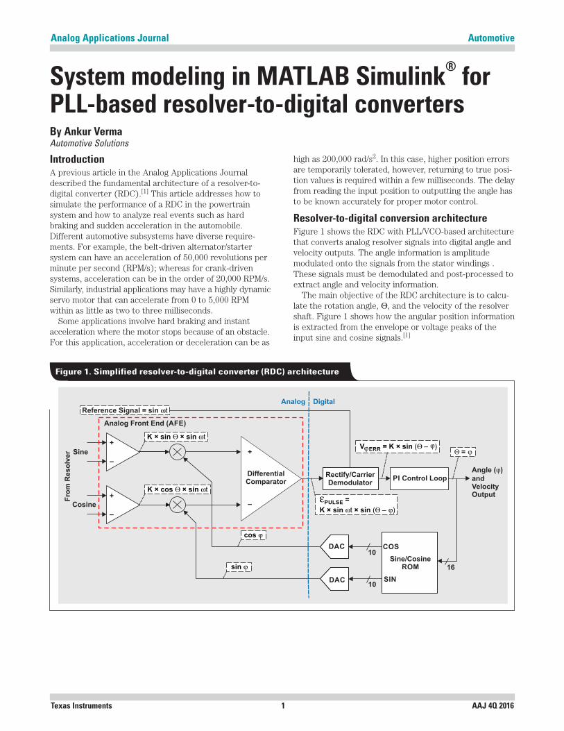
Resolver-to-digital conversion architectureFigure 1 shows the RDC with PLL/VCO-based architecture that converts analog resolver signals into digital angle and velocity outputs. The angle information is amplitude modulated onto the signals from the stator windings . These signals must be demodulated and post-processed to extract angle and velocity information.
The main objective of the RDC architecture is to calcu-late the rotation angle, Θ, and the velocity of the resolver shaft. Figure 1 shows how the angular position information is extracted from the envelope or voltage peaks of the input sine and cosine signals.[1]
By Ankur VermaAutomotive Solutions
Figure 1. Simplified resolver-to-digital converter (RDC) architecture
Angle ( )ϕandVelocityOutput
DAC
DAC
COS
Analog Digital
SIN
10
16
10
DifferentialComparator
K × sin × sin tΘ ω
Reference Signal = sin tω
V = K × sinϕERR ( – )Θ ϕΘ ϕ=
sin ϕ
Rectify/CarrierDemodulator
PI Control Loop
Sine/CosineROM
K × cos × sin tΘ ω
cos ϕ
Sine
Analog Front End (AFE)
Cosine
Fro
m R
eso
lver
+
+
+
–
–
–
εPULSE =
t ( – )K × sin × sinω Θ ϕ
Texas Instruments 2 AAJ 4Q 2016
AutomotiveAnalog Applications Journal
System modelingVarious use cases at the system level can be simulated with the help of the MATLAB Simulink-based architecture model, such as has been done for the PGA411-Q1 in Figure 2. There are two major blocks in the system model for use-case analysis of different configurations.
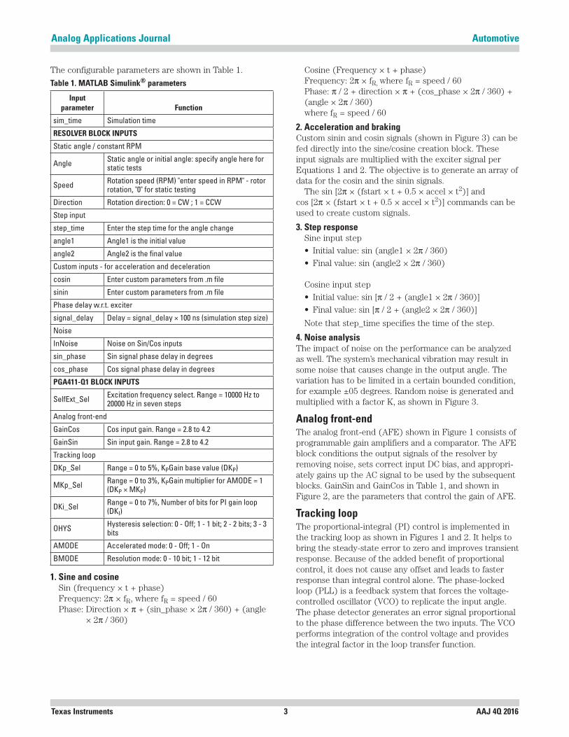
Resolver blockThe input resolver block shown in Figure 3 supports various real-system scenarios, such as:
1. Static angle testing
2. Step response in input angle
3. Custom acceleration/deceleration
4. Sudden acceleration/hard braking
5. Effects of coupled noise in the system
The outputs from the resolver blocks are simulated signals of the resolver sensor:
Sine signal from resolver sensor = sin Θ × sin wt (1)
Cosine signal from resolver sensor = cos Θ × sin wt (2)
where Θ = resolver angle and w = the exciter or excitation frequency applied at the R1-R2 rotor winding.
The amplitude-modulated signals at the sine and cosine winding of the resolver are created inside the resolver block. There are multiple ways to give inputs to this block.
Figure 2. MATLAB Simulink model for real system analysis
Figure 3. Input resolver block diagram
DifferentialComparator
PGA411-Q1
ε_pulse
threshold
Loop error
Looperrorcomp
z1
Unit Delay4
[A]
[D]
[C]
Goto 2
[B]
[E]
Goto 4
[A]
From 8
[B]
From 7
0.3
faultthreshold
Z-d
Z-d
Delay 1
-C-
GainCos
-C-
GainSin
[H]
Goto 6
-K-
Gain_Noise
phi_hys
ToWorkspace
[M]
Goto 8
IEx pins
sin input
cos input
exciter out
Exciter Phase Configuration
csin ϕ
cos ϕ
Sine/Cosine ROM DAC
ε_pulse
exciter
VϕERR
CarrierDemodulator
Vϕ_ERR
exciter
velocity
ϕ
+
–
output Θ
PI ControlLoop
K Θ sin ωtsin
K Θ sin ωtcos
K Θ sin ωtcos
K Θ sin ωtsin cos_gain
sine_gain
sin ϕ
cos ϕ
Out 1
Out 2
Mixercosin
sinin
Noise
AFE
Manual Switch 2 Manual Switch
angle
Step
Step 1
Accelerationand Braking
Delay
Goto 3
Goto 1
Goto
sin input
exciter
cos input
input anglenoise
Sine/CosineCreation
ManualSwitch 3 Manual
Switch 1
SineWave
RandomNumber
CosWave
Exciter
InputStep
FromWorkspace 1
FromWorkspace
IdealSignals
Resolver
-K-
Gain_Noise
K Θ sin ωtcos
K Θ sin ωtsin
cosin
sinin
Noise
Manual Switch 2 Manual Switch
Step
Step 1
Accelerationand Braking
sin input
exciter
cos input
input anglenoise
Sine/CosineCreation
ManualSwitch 3 Manual
Switch 1
SineWave
RandomNumber
CosWave
Exciter
InputStep
FromWorkspace 1
FromWorkspace
IdealSignals
Resolver
Texas Instruments 3 AAJ 4Q 2016
AutomotiveAnalog Applications Journal
The configurable parameters are shown in Table 1.
Table 1. MATLAB Simulink® parameters
Input parameter Function
sim_time Simulation time
RESOLVER BLOCK INPUTS
Static angle / constant RPM
Angle Static angle or initial angle: specify angle here for static tests
Speed Rotation speed (RPM) "enter speed in RPM" - rotor rotation, "0" for static testing
Direction Rotation direction: 0 = CW ; 1 = CCW
Step input
step_time Enter the step time for the angle change
angle1 Angle1 is the initial value
angle2 Angle2 is the final value
Custom inputs - for acceleration and deceleration
cosin Enter custom parameters from .m file
sinin Enter custom parameters from .m file
Phase delay w.r.t. exciter
signal_delay Delay = signal_delay × 100 ns (simulation step size)
Noise
InNoise Noise on Sin/Cos inputs
sin_phase Sin signal phase delay in degrees
cos_phase Cos signal phase delay in degrees
PGA411-Q1 BLOCK INPUTS
SelfExt_Sel Excitation frequency select. Range = 10000 Hz to 20000 Hz in seven steps
Analog front-end
GainCos Cos input gain. Range = 2.8 to 4.2
GainSin Sin input gain. Range = 2.8 to 4.2
Tracking loop
DKp_Sel Range = 0 to 5%, KPGain base value (DKP)
MKp_Sel Range = 0 to 3%, KPGain multiplier for AMODE = 1 (DKP × MKP)
DKi_Sel Range = 0 to 7%, Number of bits for PI gain loop (DKI)
OHYS Hysteresis selection: 0 - Off; 1 - 1 bit; 2 - 2 bits; 3 - 3 bits
AMODE Accelerated mode: 0 - Off; 1 - On
BMODE Resolution mode: 0 - 10 bit; 1 - 12 bit
1. Sine and cosineSin (frequency × t + phase)Frequency: 2p × fR, where fR = speed / 60Phase: Direction × p + (sin_phase × 2p / 360) + (angle
× 2p / 360)
Cosine (Frequency × t + phase)Frequency: 2p × fR, where fR = speed / 60 Phase: p / 2 + direction × p + (cos_phase × 2p / 360) + (angle × 2p / 360)where fR = speed / 60
2. Acceleration and brakingCustom sinin and cosin signals (shown in Figure 3) can be fed directly into the sine/cosine creation block. These input signals are multiplied with the exciter signal per Equations 1 and 2. The objective is to generate an array of data for the cosin and the sinin signals.
The sin [2p × (fstart × t + 0.5 × accel × t2)] and cos [2p × (fstart × t + 0.5 × accel × t2)] commands can be used to create custom signals.
3. Step response Sine input step
• Initial value: sin (angle1 × 2p / 360)
• Final value: sin (angle2 × 2p / 360)
Cosine input step
• Initial value: sin [p / 2 + (angle1 × 2p / 360)]
• Final value: sin [p / 2 + (angle2 × 2p / 360)]
Note that step_time specifies the time of the step.
4. Noise analysisThe impact of noise on the performance can be analyzed as well. The system’s mechanical vibration may result in some noise that causes change in the output angle. The variation has to be limited in a certain bounded condition, for example ±05 degrees. Random noise is generated and multiplied with a factor K, as shown in Figure 3.
Analog front-endThe analog front-end (AFE) shown in Figure 1 consists of programmable gain amplifiers and a comparator. The AFE block conditions the output signals of the resolver by removing noise, sets correct input DC bias, and appropri-ately gains up the AC signal to be used by the subsequent blocks. GainSin and GainCos in Table 1, and shown in Figure 2, are the parameters that control the gain of AFE.
Tracking loopThe proportional-integral (PI) control is implemented in the tracking loop as shown in Figures 1 and 2. It helps to bring the steady-state error to zero and improves transient response. Because of the added benefit of proportional control, it does not cause any offset and leads to faster response than integral control alone. The phase-locked loop (PLL) is a feedback system that forces the voltage-controlled oscillator (VCO) to replicate the input angle. The phase detector generates an error signal proportional to the phase difference between the two inputs. The VCO performs integration of the control voltage and provides the integral factor in the loop transfer function.
Texas Instruments 4 AAJ 4Q 2016
AutomotiveAnalog Applications Journal
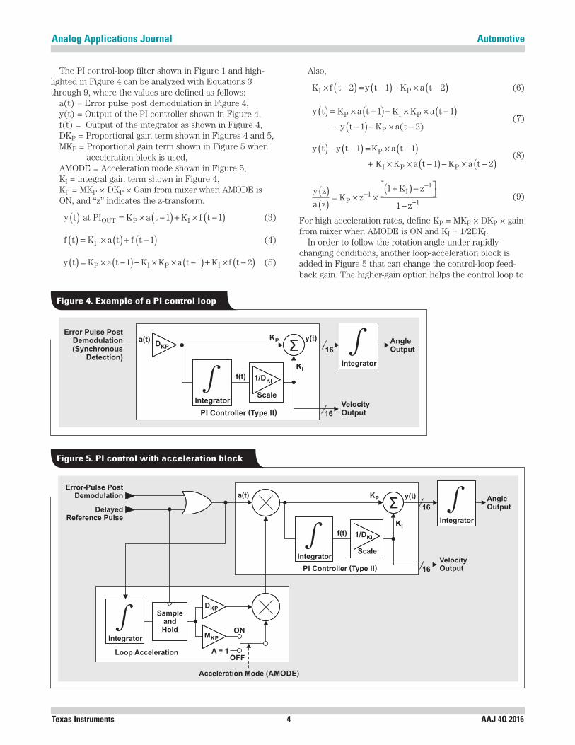
The PI control-loop filter shown in Figure 1 and high-lighted in Figure 4 can be analyzed with Equations 3 through 9, where the values are defined as follows:
a(t) = Error pulse post demodulation in Figure 4,y(t) = Output of the PI controller shown in Figure 4,f(t) = Output of the integrator as shown in Figure 4, DKP = Proportional gain term shown in Figures 4 and 5, MKP = Proportional gain term shown in Figure 5 when
acceleration block is used,AMODE = Acceleration mode shown in Figure 5,KI = integral gain term shown in Figure 4, KP = MKP × DKP × Gain from mixer when AMODE is ON, and “z” indicates the z-transform.
y t PI K a t K f tOUT P I( ) = × −( ) + × −( ) at 1 1
(3)
f t K a t f tP( ) = × ( ) + −( )1
(4)
y t K a t K K a t K f tP I P I( ) = × −( ) + × × −( ) + × −( )1 1 2
(5)
Also,
K f t y t K a tI P× −( ) = −( ) − × −( )2 1 2
(6)
y t K a t K K a t
t K a t
P I P
P
( ) = × −( ) + × × −( )+ −( ) − × −( )
1 1
1 2 y
(7)
y t y t K a t
K K a t K a t
P
I P P
( ) − −( ) = × −( )+ × × −( ) − × −( )
1 1
1 2
(8)
y z
a zK z
K z
zP
I( )( ) = × ×
+( ) −
−−
−
−1
1
1
1
1
(9)
For high acceleration rates, define KP = MKP × DKP × gain from mixer when AMODE is ON and KI = 1/2DKI.
In order to follow the rotation angle under rapidly changing conditions, another loop-acceleration block is added in Figure 5 that can change the control-loop feed-back gain. The higher-gain option helps the control loop to
Figure 5. PI control with acceleration block
Loop Acceleration
PI Controller (Type II)
MKP
DKP
Acceleration Mode (AMODE)
A = 1
ON
OFF
Σ AngleOutput
VelocityOutput
KIKI
KP
Scale
∫
∫∫
SampleandHold
Error-Pulse PostDemodulation
DelayedReference Pulse
16
16
Integrator
Integrator
Integrator
1/DKI
y(t)a(t)
f(t)
Figure 4. Example of a PI control loop
PI Controller (Type II)
Σ AngleOutput
VelocityOutput
KIKI
KP y(t)a(t)
f(t)
Scale
∫∫
Error Pulse PostDemodulation(Synchronous
Detection)16
16
Integrator
Integrator
1/DKI
DKP
Texas Instruments 5 AAJ 4Q 2016
AutomotiveAnalog Applications Journal
track a fast rotation angle much easier. In the acceleration mode, the proportional gain is increased by several times (DKP × MKP) compared to the normal mode (DKP).
VCOIntegrator =− −1
1 1z (10)
The transfer function of the PI control loop is the multi-plication of Equations 9 and 10.
Transfer Functionz
z =
−× × ×
+( ) −
−
−
−−
−
−
1
11
1
11
1
1K z
K z
zP
I
(11)
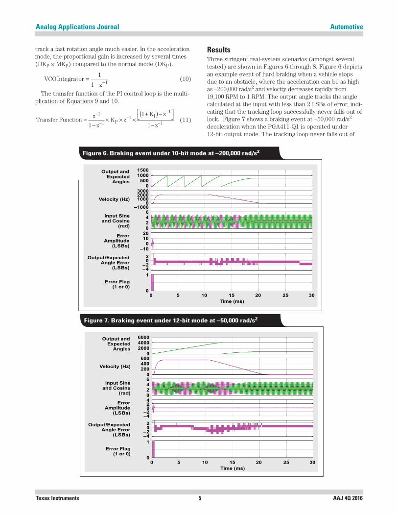
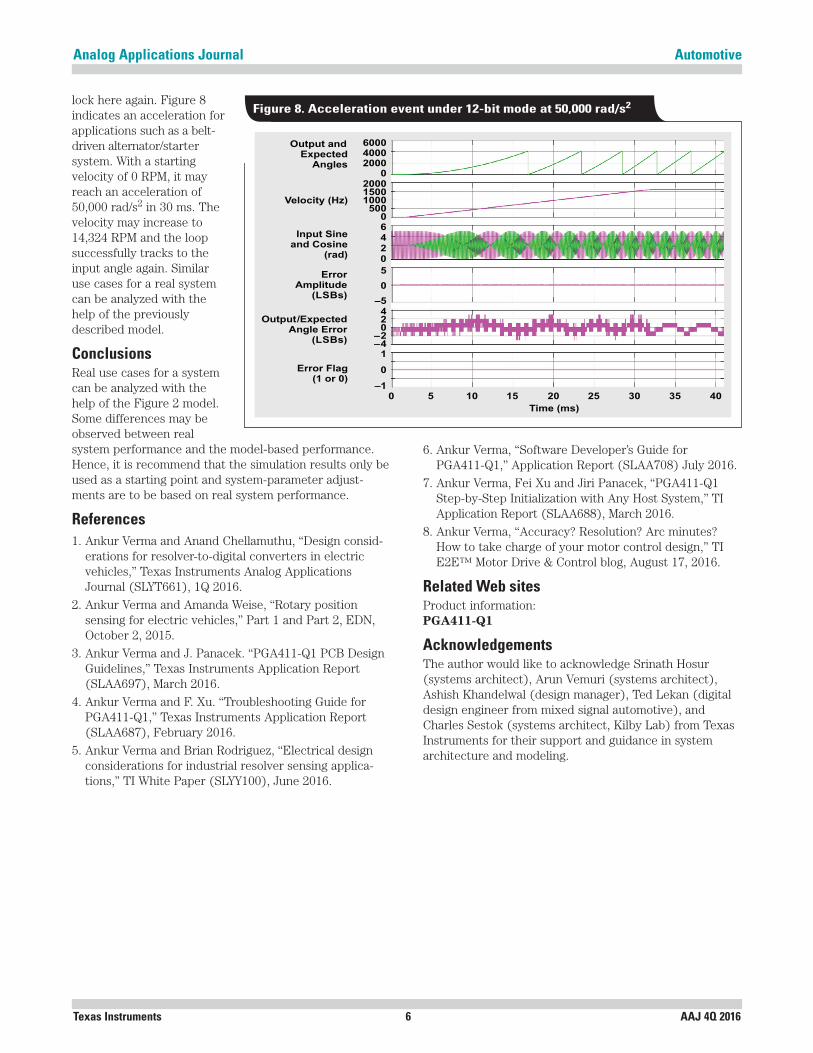
ResultsThree stringent real-system scenarios (amongst several tested) are shown in Figures 6 through 8. Figure 6 depicts an example event of hard braking when a vehicle stops due to an obstacle, where the acceleration can be as high as –200,000 rad/s2 and velocity decreases rapidly from 19,100 RPM to 1 RPM. The output angle tracks the angle calculated at the input with less than 2 LSBs of error, indi-cating that the tracking loop successfully never falls out of lock. Figure 7 shows a braking event at –50,000 rad/s2 deceleration when the PGA411-Q1 is operated under 12-bit output mode. The tracking loop never falls out of
Figure 6. Braking event under 10-bit mode at –200,000 rad/s2
15001000500
0
20100
–10
20
–2–4
1
0
6
4
2
0
300020001000
0–1000
Time (ms)
0 5 10 15 20 25 30
Output andExpected
Angles
Velocity (Hz)
Error Flag(1 or 0)
Input Sineand Cosine
(rad)
ErrorAmplitude
(LSBs)
Output/ExpectedAngle Error
(LSBs)
Figure 7. Braking event under 12-bit mode at –50,000 rad/s2
6000
4000
2000
0
420
–2–4
20
–2–4
1
0
6
4
2
0
600
400
200
0
Output andExpected
Angles
Velocity (Hz)
Error Flag(1 or 0)
Input Sineand Cosine
(rad)
ErrorAmplitude
(LSBs)
Output/ExpectedAngle Error
(LSBs)
Time (ms)
0 5 10 15 20 25 30
Texas Instruments 6 AAJ 4Q 2016
AutomotiveAnalog Applications Journal
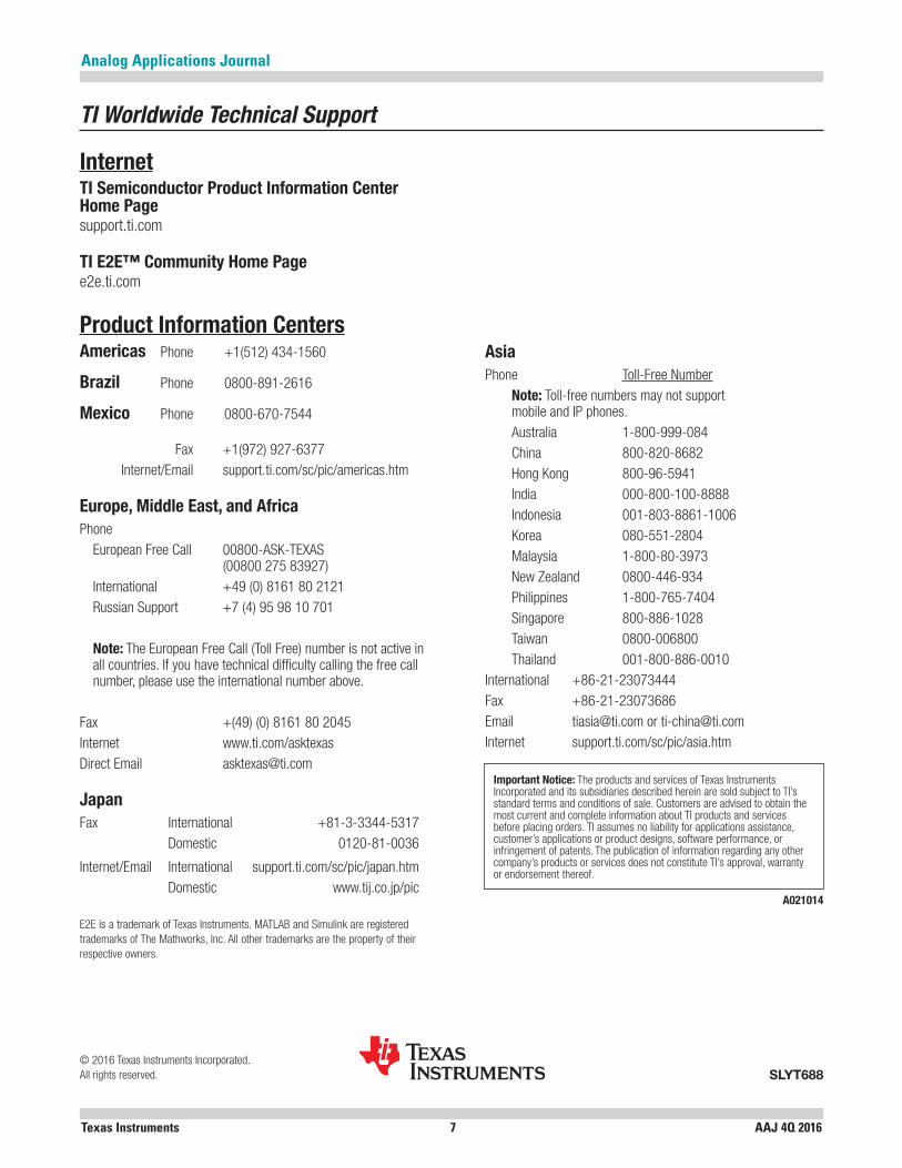
lock here again. Figure 8 indicates an acceleration for applications such as a belt-driven alternator/starter system. With a starting velocity of 0 RPM, it may reach an acceleration of 50,000 rad/s2 in 30 ms. The velocity may increase to 14,324 RPM and the loop successfully tracks to the input angle again. Similar use cases for a real system can be analyzed with the help of the previously described model.
ConclusionsReal use cases for a system can be analyzed with the help of the Figure 2 model. Some differences may be observed between real system performance and the model-based performance. Hence, it is recommend that the simulation results only be used as a starting point and system-parameter adjust-ments are to be based on real system performance.
References1. Ankur Verma and Anand Chellamuthu, “Design consid-
erations for resolver-to-digital converters in electric vehicles,” Texas Instruments Analog Applications Journal (SLYT661), 1Q 2016.
2. Ankur Verma and Amanda Weise, “Rotary position sensing for electric vehicles,” Part 1 and Part 2, EDN, October 2, 2015.
3. Ankur Verma and J. Panacek. “PGA411-Q1 PCB Design Guidelines,” Texas Instruments Application Report (SLAA697), March 2016.
4. Ankur Verma and F. Xu. “Troubleshooting Guide for PGA411-Q1,” Texas Instruments Application Report (SLAA687), February 2016.
5. Ankur Verma and Brian Rodriguez, “Electrical design considerations for industrial resolver sensing applica-tions,” TI White Paper (SLYY100), June 2016.
Figure 8. Acceleration event under 12-bit mode at 50,000 rad/s2
600040002000
0
5
0
–5420
–2–4
1
0
–1
6420
200015001000500
0
Time (ms)
0 5 10 15 20 353025 40
Output andExpected
Angles
Velocity (Hz)
Error Flag(1 or 0)
Input Sineand Cosine
(rad)
ErrorAmplitude
(LSBs)
Output/ExpectedAngle Error
(LSBs)
6. Ankur Verma, “Software Developer’s Guide for PGA411-Q1,” Application Report (SLAA708) July 2016.
7. Ankur Verma, Fei Xu and Jiri Panacek, “PGA411-Q1 Step-by-Step Initialization with Any Host System,” TI Application Report (SLAA688), March 2016.
8. Ankur Verma, “Accuracy? Resolution? Arc minutes? How to take charge of your motor control design,” TI E2E™ Motor Drive & Control blog, August 17, 2016.
Related Web sitesProduct information:PGA411-Q1
AcknowledgementsThe author would like to acknowledge Srinath Hosur (systems architect), Arun Vemuri (systems architect), Ashish Khandelwal (design manager), Ted Lekan (digital design engineer from mixed signal automotive), and Charles Sestok (systems architect, Kilby Lab) from Texas Instruments for their support and guidance in system architecture and modeling.
Texas Instruments 7 AAJ 4Q 2016
Analog Applications Journal
E2E is a trademark of Texas Instruments. MATLAB and Simulink are registered trademarks of The Mathworks, Inc. All other trademarks are the property of their respective owners.
TI Worldwide Technical Support
InternetTI Semiconductor Product Information Center Home Pagesupport.ti.com
TI E2E™ Community Home Pagee2e.ti.com
Product Information CentersAmericas Phone +1(512) 434-1560
Brazil Phone 0800-891-2616
Mexico Phone 0800-670-7544
Fax +1(972) 927-6377 Internet/Email support.ti.com/sc/pic/americas.htm
Europe, Middle East, and AfricaPhone European Free Call 00800-ASK-TEXAS (00800 275 83927) International +49 (0) 8161 80 2121 Russian Support +7 (4) 95 98 10 701
Note: The European Free Call (Toll Free) number is not active in all countries. If you have technical difficulty calling the free call number, please use the international number above.
Fax +(49) (0) 8161 80 2045Internet www.ti.com/asktexasDirect Email [email protected]
JapanFax International +81-3-3344-5317 Domestic 0120-81-0036
Internet/Email International support.ti.com/sc/pic/japan.htm Domestic www.tij.co.jp/pic
AsiaPhone Toll-Free Number Note: Toll-free numbers may not support
mobile and IP phones. Australia 1-800-999-084 China 800-820-8682 Hong Kong 800-96-5941 India 000-800-100-8888 Indonesia 001-803-8861-1006 Korea 080-551-2804 Malaysia 1-800-80-3973 New Zealand 0800-446-934 Philippines 1-800-765-7404 Singapore 800-886-1028 Taiwan 0800-006800 Thailand 001-800-886-0010International +86-21-23073444Fax +86-21-23073686Email [email protected] or [email protected] support.ti.com/sc/pic/asia.htm
A021014
Important Notice: The products and services of Texas Instruments Incorporated and its subsidiaries described herein are sold subject to TI’s standard terms and conditions of sale. Customers are advised to obtain the most current and complete information about TI products and services before placing orders. TI assumes no liability for applications assistance, customer’s applications or product designs, software performance, or infringement of patents. The publication of information regarding any other company’s products or services does not constitute TI’s approval, warranty or endorsement thereof.
© 2016 Texas Instruments Incorporated. All rights reserved. SLYT688
IMPORTANT NOTICE
Texas Instruments Incorporated and its subsidiaries (TI) reserve the right to make corrections, enhancements, improvements and otherchanges to its semiconductor products and services per JESD46, latest issue, and to discontinue any product or service per JESD48, latestissue. Buyers should obtain the latest relevant information before placing orders and should verify that such information is current andcomplete. All semiconductor products (also referred to herein as “components”) are sold subject to TI’s terms and conditions of salesupplied at the time of order acknowledgment.TI warrants performance of its components to the specifications applicable at the time of sale, in accordance with the warranty in TI’s termsand conditions of sale of semiconductor products. Testing and other quality control techniques are used to the extent TI deems necessaryto support this warranty. Except where mandated by applicable law, testing of all parameters of each component is not necessarilyperformed.TI assumes no liability for applications assistance or the design of Buyers’ products. Buyers are responsible for their products andapplications using TI components. To minimize the risks associated with Buyers’ products and applications, Buyers should provideadequate design and operating safeguards.TI does not warrant or represent that any license, either express or implied, is granted under any patent right, copyright, mask work right, orother intellectual property right relating to any combination, machine, or process in which TI components or services are used. Informationpublished by TI regarding third-party products or services does not constitute a license to use such products or services or a warranty orendorsement thereof. Use of such information may require a license from a third party under the patents or other intellectual property of thethird party, or a license from TI under the patents or other intellectual property of TI.Reproduction of significant portions of TI information in TI data books or data sheets is permissible only if reproduction is without alterationand is accompanied by all associated warranties, conditions, limitations, and notices. TI is not responsible or liable for such altereddocumentation. Information of third parties may be subject to additional restrictions.Resale of TI components or services with statements different from or beyond the parameters stated by TI for that component or servicevoids all express and any implied warranties for the associated TI component or service and is an unfair and deceptive business practice.TI is not responsible or liable for any such statements.Buyer acknowledges and agrees that it is solely responsible for compliance with all legal, regulatory and safety-related requirementsconcerning its products, and any use of TI components in its applications, notwithstanding any applications-related information or supportthat may be provided by TI. Buyer represents and agrees that it has all the necessary expertise to create and implement safeguards whichanticipate dangerous consequences of failures, monitor failures and their consequences, lessen the likelihood of failures that might causeharm and take appropriate remedial actions. Buyer will fully indemnify TI and its representatives against any damages arising out of the useof any TI components in safety-critical applications.In some cases, TI components may be promoted specifically to facilitate safety-related applications. With such components, TI’s goal is tohelp enable customers to design and create their own end-product solutions that meet applicable functional safety standards andrequirements. Nonetheless, such components are subject to these terms.No TI components are authorized for use in FDA Class III (or similar life-critical medical equipment) unless authorized officers of the partieshave executed a special agreement specifically governing such use.Only those TI components which TI has specifically designated as military grade or “enhanced plastic” are designed and intended for use inmilitary/aerospace applications or environments. Buyer acknowledges and agrees that any military or aerospace use of TI componentswhich have not been so designated is solely at the Buyer's risk, and that Buyer is solely responsible for compliance with all legal andregulatory requirements in connection with such use.TI has specifically designated certain components as meeting ISO/TS16949 requirements, mainly for automotive use. In any case of use ofnon-designated products, TI will not be responsible for any failure to meet ISO/TS16949.
Products ApplicationsAudio www.ti.com/audio Automotive and Transportation www.ti.com/automotiveAmplifiers amplifier.ti.com Communications and Telecom www.ti.com/communicationsData Converters dataconverter.ti.com Computers and Peripherals www.ti.com/computersDLP® Products www.dlp.com Consumer Electronics www.ti.com/consumer-appsDSP dsp.ti.com Energy and Lighting www.ti.com/energyClocks and Timers www.ti.com/clocks Industrial www.ti.com/industrialInterface interface.ti.com Medical www.ti.com/medicalLogic logic.ti.com Security www.ti.com/securityPower Mgmt power.ti.com Space, Avionics and Defense www.ti.com/space-avionics-defenseMicrocontrollers microcontroller.ti.com Video and Imaging www.ti.com/videoRFID www.ti-rfid.comOMAP Applications Processors www.ti.com/omap TI E2E Community e2e.ti.comWireless Connectivity www.ti.com/wirelessconnectivity
Mailing Address: Texas Instruments, Post Office Box 655303, Dallas, Texas 75265Copyright © 2016, Texas Instruments Incorporated