systematically controlling kapitza conductance via ... · systematically controlling kapitza...
TRANSCRIPT
Systematically controlling Kapitza conductance via chemical etchingJohn C. Duda and Patrick E. Hopkins Citation: Appl. Phys. Lett. 100, 111602 (2012); doi: 10.1063/1.3695058 View online: http://dx.doi.org/10.1063/1.3695058 View Table of Contents: http://apl.aip.org/resource/1/APPLAB/v100/i11 Published by the American Institute of Physics. Related ArticlesRole of ethylene on surface oxidation of TiO2(110) Appl. Phys. Lett. 101, 211601 (2012) Bidirectionally tuning Kapitza conductance through the inclusion of substitutional impurities J. Appl. Phys. 112, 073519 (2012) Communication: An obligatory glass surface J. Chem. Phys. 137, 141102 (2012) Pressure dependency of thermal boundary conductance of carbon nanotube/silicon interface: A moleculardynamics study J. Appl. Phys. 112, 053501 (2012) Effect of nanopatterns on Kapitza resistance at a water-gold interface during boiling: A molecular dynamics study J. Appl. Phys. 112, 053508 (2012) Additional information on Appl. Phys. Lett.Journal Homepage: http://apl.aip.org/ Journal Information: http://apl.aip.org/about/about_the_journal Top downloads: http://apl.aip.org/features/most_downloaded Information for Authors: http://apl.aip.org/authors
Downloaded 28 Dec 2012 to 137.54.10.198. Redistribution subject to AIP license or copyright; see http://apl.aip.org/about/rights_and_permissions
Systematically controlling Kapitza conductance via chemical etching
John C. Duda1,2,a) and Patrick E. Hopkins1,b)
1Department of Mechanical and Aerospace Engineering, University of Virginia, Charlottesville,Virginia 22904, USA2Microscale Science and Technology Department, Sandia National Laboratories, Albuquerque,New Mexico 87185, USA
(Received 23 January 2012; accepted 29 February 2012; published online 15 March 2012)
We measure the thermal interface conductance between thin aluminum films and silicon substrates
via time-domain thermoreflectance from 100 to 300 K. The substrates are chemically etched prior
to aluminum deposition, thereby offering a means of controlling interface roughness. We find that
conductance can be systematically varied by manipulating roughness. In addition, transmission
electron microscopy confirms the presence of a conformal oxide for all roughnesses, which is then
taken into account via a thermal resistor network. This etching process provides a robust technique for
tuning the efficiency of thermal transport while alleviating the need for laborious materials growth
and/or processing. VC 2012 American Institute of Physics. [http://dx.doi.org/10.1063/1.3695058]
Advances in micro- and nano-technology have led to the
development of a wide array of devices, all of which share
one common feature: characteristic length scales on the order
of a few to hundreds of nanometers. At the same time, this
ongoing trend of miniaturization has had a significant auxil-
iary impact on the thermal transport properties of modern
devices as well, insofar as they are now dictated more so by
the interfaces between constituent materials than by the
materials themselves.1 As a result, a significant effort has
been put forth to both investigate and explain the behavior of
thermal transport across solid-solid interfaces, the efficiency
of which can be described by the thermal interface conduct-
ance, or Kapitza conductance, hK.2 Prior works have demon-
strated how the mismatch of phonon spectra,3–7 interfacial
chemistry and bonding,8–15 crystallographic orientation,16–21
and interfacial roughness5,22–28 can each influence Kapitza
conductance.
Generally speaking, the expression “interfacial rough-
ness” can include one or a combination of several unique
structural features, including compositional mixing, dis-
locations, interstitials, deviations from crystallinity, or
nanometer-scale geometric facets. When compared to that at
a nominally “smooth” interface, certain combinations of
these features have been found to enhance Kapitza conduct-
ance,5,28 while others have been shown to reduce it.5,22,24–26
Furthermore, it has been shown that thermal transport effi-
ciency can be effectively tuned if precise control over inter-
facial roughness is possible. For example, Pernot et al.29 and
Hopkins et al.25 demonstrated that controlling interface
roughness through quantum-dot patterning can reduce the
effective thermal conductivity of silicon-based superlattices
and the Kapitza conductance at aluminum-silicon interfaces,
respectively. However, other methods of interface roughen-
ing, including chemical treatments26 and back-sputtering,22
have not yet been shown to provide precise enough control
over roughness to systematically and repeatably alter inter-
face conductance.
In this letter, we demonstrate that chemically etching
substrates prior to thin-film deposition can, in fact, provide
the precise control over interfacial roughness required to sys-
tematically tune Kapitza conductance without the need for
laborious materials growth and/or processing, e.g., quantum-
dot patterning. Cross-section transmission electron micros-
copy (TEM) confirms that the roughness induced by chemi-
cal etching does not lead to compositional mixing between
aluminum and silicon due to the presence of a thin and con-
formal native oxide (<2 nm), nor a deviation from crystallin-
ity in either the film or the substrate. The Kapitza
conductances at four aluminum-silicon interfaces of varying
roughness are measured by time-domain thermoreflectance
(TDTR) and are correlated to the root-mean-square (RMS)
surface roughness of the interface. It is found that Kapitza
conductance exhibits an exponential dependence on interface
roughness consistent with prior experimental data and as
described by previous models.24,25 In addition, it is found
that as roughness increases, the temperature dependence of
Kapitza conductance is substantially suppressed.
We prepared four different aluminum-silicon interfaces
by evaporating 80 nm of aluminum (vacuum pressure < 10
� 10�7 Torr) on silicon substrates. The silicon wafers are
each 500 lm thick, phosphorus doped (n-type), and single
crystalline (100). Prior to deposition, all substrates were first
cleaned with methanol and acetone and then rinsed in de-
ionized water. Sample I received no further processing,
whereas samples II through IV were treated in buffered oxide
etch (BOE) to remove the native oxide and then submersed in
tetramethyl ammonium hydroxide (TMAH) at 80 �C in order
to roughen the substrates in a fashion similar to Ref. 26. After
surface pretreatment, all samples were left exposed to ambient
for 24 h to allow a native oxide to reform on the surface. The
RMS surface roughnesses, d, of the samples were determined
prior to aluminum thin film deposition via atomic force mi-
croscopy (AFM). Substrate surface roughness increased with
the time submersed in the TMAH solution. The measured
RMS surface roughnesses and room-temperature Kapitza con-
ductances of the four samples, along with the repeatability of
the measurements, are listed in Table I.
a)Electronic mail: [email protected])Electronic mail: [email protected].
0003-6951/2012/100(11)/111602/4/$30.00 VC 2012 American Institute of Physics100, 111602-1
APPLIED PHYSICS LETTERS 100, 111602 (2012)
Downloaded 28 Dec 2012 to 137.54.10.198. Redistribution subject to AIP license or copyright; see http://apl.aip.org/about/rights_and_permissions
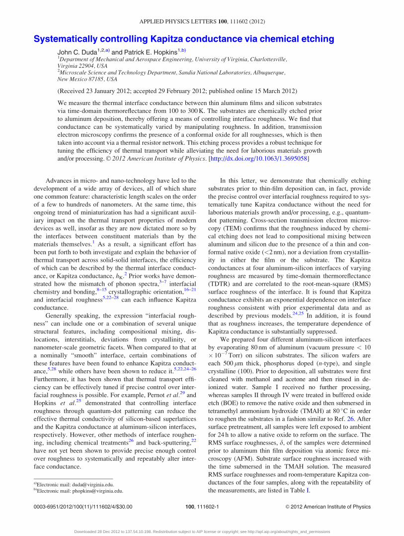
Cross-sectional TEM was implemented to further char-
acterize the roughnesses and quality of the interfaces post
aluminum thin film deposition. Micrographs of samples I
and IV at two different magnifications are shown in Fig. 1.
The micrographs indicate that regardless of roughness, an
approximately 1.75 nm thick conformal oxide layer covers
the silicon substrates after 24-h exposure to ambient. This
oxide layer prohibits any apparent interdiffusion or composi-
tional mixing of aluminum and silicon at the interface, as
opposed to earlier studies of chromium-silicon interfaces
where Auger electron spectroscopy confirmed a significant
mixing of species within roughly 10 nm of the interface.22 In
addition, the micrographs indicate that the aluminum thin
films exhibit a columnar crystal structure regardless of sub-
strate roughness, and that the crystallinity of the substrate is
undisturbed by the etch. Again, this is contrary to the afore-
mentioned chromium-silicon study, where TEM indicated
the chromium films were amorphous.22
We measured the Kapitza conductance across the four
aluminum-silicon interfaces with TDTR.30,31 TDTR is a
non-contact, pump-probe technique in which a modulated
short pulse laser (full-width half max� 100 fs) is used to cre-
ate a heating event (pump) on the surface of a sample. This
heating event is monitored with a time-delayed probe pulse.
The change in the reflectivity of the probe at the modulation
frequency of the pump is detected through a lock-in ampli-
fier; the change in reflectivity is related to the change in tem-
perature at the sample surface. This temporal thermal
response is then related to the thermophysical properties of
the sample of interest. We monitor the thermoreflectance sig-
nal over 4.5 ns of probe delay time. The deposited energy
takes approximately 100 ps to propagate through the alumi-
num film, after which the response is related to the heat flow
across the aluminum-silicon interface and the thermal effu-
sivity of the silicon substrate. Our specific experimental
setup is described in detail elsewhere.32
We monitor is the ratio of the in-phase to the out-of-
phase voltage recorded by the lock-in amplifier (�Vin/Vout),
which is related to the temperature change on the surface of
the sample. The thermal model and analysis used to predict
the temperature change and subsequent lock-in ratio are
described in detail in references 30, 32, and 33. In short, the
model accounts for heat transfer in composite slabs34 from a
periodic, Gaussian source (pump) convoluted with a Gaus-
sian sampling spot (probe).30,34 The pump is modulated at
11 MHz and the pump and probe 1/e2 radii are 7.5 lm. The
temperature change at the surface is related to the thermal
conductivity and heat capacity of the composite slabs, as
well as the Kapitza conductance between each slab.
Although dominated by the aluminum-silicon Kapitza con-
ductance,32 the TDTR signal is also related to the heat
capacity and thickness of the Al film and the thermal proper-
ties of the silicon substrate (which, due to time delay and
modulation frequency can be taken as semi-infinite in this
work). We first assume bulk values for the properties of the
film and substrate35 and we verify the aluminum film thick-
ness via picosecond acoustics.36,37 We then adjust the ther-
mal conductivity of the substrate during our analysis to
achieve a better fit between the model and the data.3
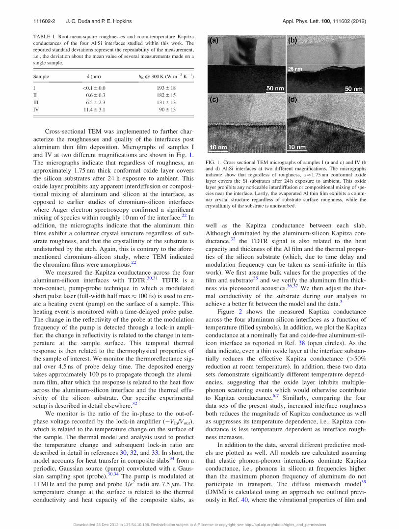
Figure 2 shows the measured Kaptiza conductance
across the four aluminum-silicon interfaces as a function of
temperature (filled symbols). In addition, we plot the Kapitza
conductance at a nominally flat and oxide-free aluminum-sil-
icon interface as reported in Ref. 38 (open circles). As the
data indicate, even a thin oxide layer at the interface substan-
tially reduces the effective Kapitza conductance (>50%
reduction at room temperature). In addition, these two data
sets demonstrate significantly different temperature depend-
encies, suggesting that the oxide layer inhibits multiple-
phonon scattering events which would otherwise contribute
to Kapitza conductance.6,7 Similarly, comparing the four
data sets of the present study, increased interface roughness
both reduces the magnitude of Kapitza conductance as well
as suppresses its temperature dependence, i.e., Kapitza con-
ductance is less temperature dependent as interface rough-
ness increases.
In addition to the data, several different predictive mod-
els are plotted as well. All models are calculated assuming
that elastic phonon-phonon interactions dominate Kapitza
conductance, i.e., phonons in silicon at frequencies higher
than the maximum phonon frequency of aluminum do not
participate in transport. The diffuse mismatch model39
(DMM) is calculated using an approach we outlined previ-
ously in Ref. 40, where the vibrational properties of film and
TABLE I. Root-mean-square roughnesses and room-temperature Kapitza
conductances of the four Al:Si interfaces studied within this work. The
reported standard deviations represent the repeatability of the measurement,
i.e., the deviation about the mean value of several measurements made on a
single sample.
Sample d (nm) hK @ 300 K (W m�2 K�1)
I <0.1 6 0.0 193 6 18
II 0.6 6 0.3 182 6 15
III 6.5 6 2.3 131 6 13
IV 11.4 6 3.1 90 6 13
FIG. 1. Cross sectional TEM micrographs of samples I (a and c) and IV (b
and d) Al:Si interfaces at two different magnifications. The micrographs
indicate show that regardless of roughness, a� 1.75 nm conformal oxide
layer covers the Si substrates after 24 h exposure to ambient. This oxide
layer prohibits any noticeable interdiffusion or compositional mixing of spe-
cies near the interface. Lastly, the evaporated Al thin film exhibits a colum-
nar crystal structure regardless of substrate surface roughness, while the
crystallinity of the substrate is undisturbed.
111602-2 J. C. Duda and P. E. Hopkins Appl. Phys. Lett. 100, 111602 (2012)
Downloaded 28 Dec 2012 to 137.54.10.198. Redistribution subject to AIP license or copyright; see http://apl.aip.org/about/rights_and_permissions
substrate are approximated by fitting polynomials to the pho-
non dispersion curves of aluminum41 and silicon42 along the
[100] crystallographic direction; assumed spherical Brillouin
zones are then constructed via an isotropic revolution of
these polynomial fits in wavevector space. As seen in Fig. 2,
the prediction of the DMM falls between the data of Ref. 38
and that at the smoothest interface presently considered. This
suggests that without an oxide layer, inelastic phonon-
phonon scattering could play a role in thermal transport
across aluminum-silicon interfaces.6,7 On the other hand, we
attribute the difference between the predicted and measured
values at the smoothest interface considered (black squares)
to the native oxide layer. The conductance of this oxide layer
is described by its thermal conductivity divided by its
thickness,
hoxide ¼ joxide=toxide: (1)
When evaluating Eq. (1), we use the temperature-dependent
bulk thermal conductivity of a:SiO2, as it has been shown
that the thermal conductivity of thin-film a:SiO2 does not
substantially differ from that of bulk.16,43 A series-resistor
approach then yields
hK ¼ ðh�1K;DMM þ h�1
oxide�1: (2)
This prediction is represented by the solid black line in
Fig. 2 and agrees well with our experimental data.
In order to take interfacial roughness into account, we
introduce a spectral attenuation coefficient previously pro-
posed by the authors,24,25 and insert this coefficient into the
integral expression of the DMM. This coefficient, c, is unity
when the phonon wavelength, k, is greater than the RMS
roughness, d. On the other hand, c¼ exp[�(4pb/k)d] when
k< d. That is, phonons with wavelengths greater than d are
unaffected by the roughness of the interface, whereas those
with wavelengths less than d are affected in a fashion similar
to that of photons in an absorptive media, e.g., the Beer-
Lambert law. Qualitatively speaking, this approach suggests
that as the "absorptivity" of the interface increases, so too
does the temperature drop across it. With the spectral attenu-
ation coefficient implemented, the DMM is once again plot-
ted in Fig. 2 for roughnesses of 6.5 nm and 11.4 nm. We find
that a value of b¼ 0.04 works well across all data sets. As is
evident in the plot, this approach not only captures the reduc-
tion in Kapitza conductance due to interface roughening, but
captures the reduction in temperature-dependence as well.
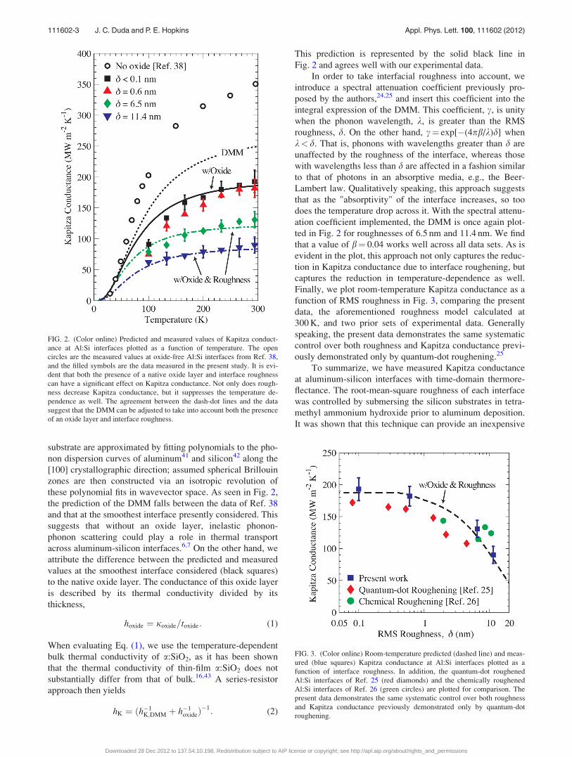
Finally, we plot room-temperature Kapitza conductance as a
function of RMS roughness in Fig. 3, comparing the present
data, the aforementioned roughness model calculated at
300 K, and two prior sets of experimental data. Generally
speaking, the present data demonstrates the same systematic
control over both roughness and Kapitza conductance previ-
ously demonstrated only by quantum-dot roughening.25
To summarize, we have measured Kapitza conductance
at aluminum-silicon interfaces with time-domain thermore-
flectance. The root-mean-square roughness of each interface
was controlled by submersing the silicon substrates in tetra-
methyl ammonium hydroxide prior to aluminum deposition.
It was shown that this technique can provide an inexpensive
FIG. 2. (Color online) Predicted and measured values of Kapitza conduct-
ance at Al:Si interfaces plotted as a function of temperature. The open
circles are the measured values at oxide-free Al:Si interfaces from Ref. 38,
and the filled symbols are the data measured in the present study. It is evi-
dent that both the presence of a native oxide layer and interface roughness
can have a significant effect on Kapitza conductance. Not only does rough-
ness decrease Kapitza conductance, but it suppresses the temperature de-
pendence as well. The agreement between the dash-dot lines and the data
suggest that the DMM can be adjusted to take into account both the presence
of an oxide layer and interface roughness.
FIG. 3. (Color online) Room-temperature predicted (dashed line) and meas-
ured (blue squares) Kapitza conductance at Al:Si interfaces plotted as a
function of interface roughness. In addition, the quantum-dot roughened
Al:Si interfaces of Ref. 25 (red diamonds) and the chemically roughened
Al:Si interfaces of Ref. 26 (green circles) are plotted for comparison. The
present data demonstrates the same systematic control over both roughness
and Kapitza conductance previously demonstrated only by quantum-dot
roughening.
111602-3 J. C. Duda and P. E. Hopkins Appl. Phys. Lett. 100, 111602 (2012)
Downloaded 28 Dec 2012 to 137.54.10.198. Redistribution subject to AIP license or copyright; see http://apl.aip.org/about/rights_and_permissions
and scalable process for tuning Kapitza conductance at solid-
solid interfaces by more than a factor of two at room
temperature.
J.C.D. is appreciative for funding from the National Sci-
ence Foundation through the Graduate Research Fellowship
Program. The authors acknowledge funding from the
National Science Foundation (CBET-1134311) and Evans
Analytical Group for the TEM data. This work was funded
in part by the LDRD program office at Sandia National Lab-
oratories. Sandia National Laboratories is a multiprogram
laboratory managed and operated by Sandia Corporation, a
wholly owned subsidiary of Lockheed Martin Corporation,
for the United States Department of Energy’s National Nu-
clear Security Administration under Contract DE-AC04-
94AL85000.
1E. Pop, S. Sinha, and K. E. Goodson, Proc. IEEE 94, 1587 (2006).2P. L. Kapitza, Phys. Rev. 60, 354 (1941).3R. J. Stoner and H. J. Maris, Phys. Rev. B 48, 16373 (1993).4R. J. Stevens, A. N. Smith, and P. M. Norris, J. Heat Transfer 127, 315
(2005).5R. J. Stevens, L. V. Zhigilei, and P. M. Norris, Int. J. Heat Mass Transfer
50, 3977 (2007).6P. E. Hopkins, P. M. Norris, and R. J. Stevens, J. Heat Transfer 130,
022401 (2008).7P. M. Norris and P. E. Hopkins, J. Heat Transfer 131, 043207 (2009).8M. Hu, P. Keblinski, and P. K. Schelling, Phys. Rev. B 79, 104305 (2009).9K. C. Collins, S. Chen, and G. Chen, Appl. Phys. Lett. 97, 083102 (2010).
10Z.-Y. Ong and E. Pop, Phys. Rev. B 81, 155408 (2010).11Y. Wang and P. Keblinski, Appl. Phys. Lett. 99, 073112 (2011).12J. C. Duda, T. S. English, E. S. Piekos, W. A. Soffa, L. V. Zhigilei, and P.
E. Hopkins, Phys. Rev. B 84, 193301 (2011).13W.-P. Hsieh, A. S. Lyons, E. Pop, P. Keblinski, and D. G. Cahill, Phys.
Rev. B 84, 184107 (2011).14M. Shen, W. J. Evans, D. Cahill, and P. Keblinski, Phys. Rev. B 84,
195432 (2011).15P. E. Hopkins, M. Baraket, E. V. Barnat, T. E. Beechem, S. P. Kearney, J.
C. Duda, J. T. Robinson, and S. G. Walton, Nano Lett. 12, 590 (2012).16R. M. Costescu, M. A. Wall, and D. G. Cahill, Phys. Rev. B 67, 054302
(2003).17R. Prasher, Phys. Rev. B 77, 075424 (2008).
18J. C. Duda, J. L. Smoyer, P. M. Norris, and P. E. Hopkins, Appl. Phys.
Lett. 95, 031912 (2009).19P. E. Hopkins, T. Beechem, J. C. Duda, K. Hattar, J. F. Ihlefeld, M. A.
Rodriguez, and E. S. Piekos, Phys. Rev. B 84, 125408 (2011).20J. Hirotani, T. Ikuta, T. Nishiyama, and K. Takahashi, Nanotechnology 22,
315702 (2011).21J. C. Duda, W. A. Soffa, R. E. Jones, C. J. Kimmer, and P. E. Hopkins,
“Influence of Crystallographic Orientation and Anisotropy on Kapitza
Conductance” (unpublished).22P. E. Hopkins, P. M. Norris, R. J. Stevens, T. E. Beechem, and S. Graham,
J. Heat Transfer 130, 062402 (2008).23Y. Xu, R. Kato, and M. Goto, J. Appl. Phys. 108, 104317 (2010).24P. E. Hopkins, J. C. Duda, S. P. Clark, C. P. Hains, T. J. Rotter, L. M.
Phinney, and G. Balakrishnan, Appl. Phys. Lett. 98, 161913 (2011).25P. E. Hopkins, J. C. Duda, C. W. Petz, and J. A. Floro, Phys. Rev. B 84,
035438 (2011).26P. E. Hopkins, L. M. Phinney, J. R. Serrano, and T. E. Beechem, Phys.
Rev. B 82, 085307 (2010).27H. Zhao and J. B. Freund, J. Appl. Phys. 105, 013515 (2009).28T. S. English, J. C. Duda, J. L. Smoyer, D. A. Jordan, P. M. Norris, and L.
V. Zhigilei, Phys. Rev. B 85, 035438 (2012).29G. Pernot, M. Stoffel, I. Savic, F. Pezzoli, P. Chen, G. Savelli, A. Jacquot,
J. Schumann, U. Denker, I. Monch et al., Nature Mater. 9, 491 (2010).30D. G. Cahill, Rev. Sci. Instrum. 75, 5119 (2004).31D. G. Cahill, K. Goodson, and A. Majumdar, J. Heat Transfer 124, 223
(2002).32P. E. Hopkins, J. R. Serrano, L. M. Phinney, S. P. Kearney, T. W. Grasser,
and C. T. Harris, J. Heat Transfer 132, 081302 (2010).33A. J. Schmidt, X. Chen, and G. Chen, Rev. Sci. Instrum. 79, 114902 (2008).34H. S. Carslaw and J. C. Jaeger, Conduction of Heat in Solids, 2nd ed.
(Clarendon, Oxford, 1959).35C. Y. Ho, R. W. Powell, and P. E. Liley, J. Phys. Chem. Ref. Data 1, 279
(1972).36C. Thomsen, J. Strait, Z. Vardeny, H. J. Maris, J. Tauc, and J. J. Hauser,
Phys. Rev. Lett. 53, 989 (1984).37C. Thomsen, H. T. Grahn, H. J. Maris, and J. Tauc, Phys. Rev. B 34, 4129
(1986).38A. J. Minnich, J. A. Johnson, A. J. Schmidt, K. Esfarjani, M. S. Dressel-
haus, K. A. Nelson, and G. Chen, Phys. Rev. Lett. 107, 095901 (2011).39E. T. Swartz and R. O. Pohl, Rev. Mod. Phys. 61, 605 (1989).40J. C. Duda, T. E. Beechem, J. L. Smoyer, P. M. Norris, and P. E. Hopkins,
J. Appl. Phys. 108, 073515 (2010).41G. Gilat and R. M. Nicklow, Phys. Rev. 143, 487 (1966).42W. Weber, Phys. Rev. B 15, 4789 (1977).43D. G. Cahill, A. Bullen, and S.-M. Lee, High Temp.-High Press. 32, 135
(2000).
111602-4 J. C. Duda and P. E. Hopkins Appl. Phys. Lett. 100, 111602 (2012)
Downloaded 28 Dec 2012 to 137.54.10.198. Redistribution subject to AIP license or copyright; see http://apl.aip.org/about/rights_and_permissions