t8xc5121 starter kit user guide - digi-key sheets/atmel pdfs/t8xc5121... · • smart card...
TRANSCRIPT
T8xC5121 Starter Kit.............................................................................................
User Guide


T8xC5121 Starter Kit User Guide
Section 1Introduction ........................................................................................... 1-1
1.1 Features....................................................................................................1-1
Section 2Getting Started...................................................................................... 1-3
2.1 Package Contents.....................................................................................1-32.2 PC System Requirements.........................................................................1-32.3 Quick Start ................................................................................................1-32.4 Connecting the Microcontroller .................................................................1-32.5 Hardware Connection ...............................................................................1-52.6 Power Supply ............................................................................................1-5
Section 3Hardware Description ........................................................................... 1-7
3.1 Description of Jumpers .............................................................................1-83.2 Description of Switches.............................................................................1-83.3 Reset.........................................................................................................1-93.4 Clock .........................................................................................................1-93.5 EA Switch..................................................................................................1-93.6 INT1 Switch...............................................................................................1-93.7 Serial Port .................................................................................................1-93.8 LEDs .........................................................................................................1-93.9 Smart Card Interface.................................................................................1-93.10 SIM Card Interface..................................................................................1-10
Section 4Microcontroller Programming.............................................................. 1-11
4.1 FLIP Software .........................................................................................1-114.2 Programming the T89C5121...................................................................1-114.3 Programming the T85C5121...................................................................1-13
Section 5Software Description........................................................................... 1-15
5.1 Programming Using FLIP........................................................................1-155.2 Running the Demonstration Program......................................................1-17
Section 6Appendix A ......................................................................................... 1-19
6.1 Schematics .............................................................................................1-216.2 References..............................................................................................1-266.3 Acronyms ................................................................................................1-26
1
4186D–SCR–06/03


Section 1
Introduction
The T8xC5121 Starter Kit allows you to fully evaluate the T8xC5121 microcontrollers.You can run either the included demonstration program or your own application.
The board can also be used as a programmer for the T89C5121 product.
The T8xC5121 Demonstration Board supports communication through RS-232 serialcommunication mode.
This user’s guide describes the hardware of the Demonstration Board as well as docu-mentation about the demonstration software.
1.1 Features • The Demonstration Board Contains Either:– Stand-alone Mode With the On-chip EEPROM Program Memory (T89C5121 Product
Version) or,– On-board EEPROM Program Memory
• In-System Programmable (ISP) via the ROM Bootloader that Downloads HEX Files Into Internal RAM Memory
• Smart Card Connector• SIM Connector• 2 LEDS• On-board Voltage Regulator with Voltage Setting• Sockets: SSOP24, DIL24 for Package Adapter• RS-232 Serial Port• Interrupt (INT1) Input• Manual Reset Switch• Data, Address and Control Lines Conveniently Brought Out on Connectors• Prototyping Area
T8xC5121 Starter Kit User Guide 1-1
Rev. 4186D–SCR–06/03

Introduction
Figure 1. T8xC5121 Starter Kit
1-2 T8xC5121 Starter Kit User Guide
4186D–SCR–06/03
Section 2
Getting Started
2.1 Package Contents
� T8xC5121 Demonstration Board
� T85C5121 and T89C5121 Microcontrollers
� MPCOS EMV smart card
� SSOP24 Adapter
� CD-ROM with Software and Documentation
– FLIP software for In-System Programming
– Quickterm Software for Demonstration
Note: A direct serial cable (DB9) and a power supply are not provided.
2.2 PC System Requirements
� 486 processor
� 16 MB RAM
� 12 MB Free disk Space
� Windows 98®, Windows NT®, XP or Windows 2000®
2.3 Quick Start The T8xC5121 D Starter Kit is shipped with a T85C5121 and T89C5121 microcontroller.
The demonstration board and accompanying software allow you to read data from asmartcard and display it on a host PC.
You can also load your own application (in .hex file format) to retrieve data from a smart-card or a credit card.
2.4 Connecting the Microcontroller
The T8xC5121 Demonstration Board is designed to support two different microcontrol-lers, T85C5121 and T89C5121.
The microcontrollers are connected either on the bottom or top of the board, respec-tively.The T89C5121 requires the use of the SSOP24 Adapter which must be plugged into theDIL support. Alternatively, the T89C5121 can be soldered on the board.
T8xC5121 Starter Kit User Guide 2-3
Rev. 4186D–SCR–06/03
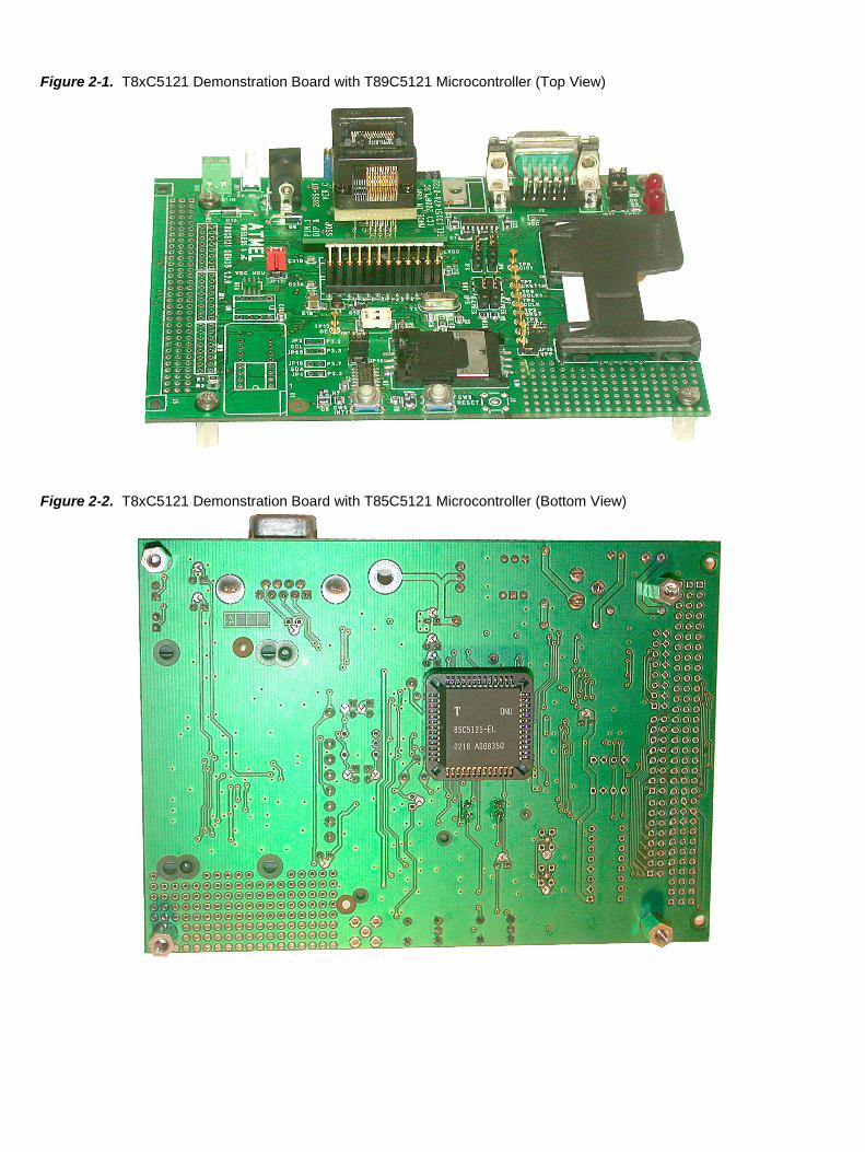
Figure 2-1. T8xC5121 Demonstration Board with T89C5121 Microcontroller (Top View)
Figure 2-2. T8xC5121 Demonstration Board with T85C5121 Microcontroller (Bottom View)

Getting Started
2.5 Hardware Connection
1. A 9 - 12V power supply must be connected to the J3 connector.
2. A serial cable must first be attached between COM PC port and J2 DB9 connec-tor of the demonstration board.
3. Ensure the T89C5121 or the T85C5121 microcontroller is connected to the board.
4. The ON/OFF Switch (SW3) must be ON. See Figure 3-1.
The Board is delivered with one 14.7456 MHz quartz (Y2).
2.6 Power Supply
2.6.1 Board Supply The Board can be powered from:
� “9V DC IN” J3 Power connector
� “9V DC IN” JR1 connector for battery connection
� “3 - 5V DC IN” JH2 connector connected to VCC/VSS Signals
� RS-232 Connector using Pin 9 and JP3 Connector
In the first two configurations the potentiometer R23 is used to adjust the VCC level.
In the last two configurations VCC is directly connected to the board.
Table 2-1 outlines the isolated Power Supply control for the demonstration board andmicrocontroller.
Table 2-1. Power Supply Control Settings
2.6.2 Internal Voltages Three test points are provided to monitor the internal voltages.
Table 2-2. Test Points Table
Reference Designation Switch On/Off Test Point Jumpers Function
Vcc Product Power Supply SW3 TP11 JP1 Global Vcc
Vcc Microcontroller Power Supply JP17 MCU Vcc
Reference Designation Test Point
DVCC Core regulated voltage (3V) TP14
EVCC UART power supply TP10
CVCC Smart Card Supply TP2
T8xC5121 Starter Kit User Guide 2-5
4186D–SCR–06/03

Getting Started
2-6 T8xC5121 Starter Kit User Guide
4186D–SCR–06/03

Section 3
Hardware DescriptionFigure 3-1. T8xC5121 Demonstration Board Components
Note: 1. On solder side.
JP17
SW3
JP1
JP6
JP5JP13 JP14
JP8 JP15
JP9
JP7
JP11 JP16
SW2 Reset JP19
SmartCard
Slot
U1
LED
LED
PLCCSocket(1)
Y2SSOP24 DIL24
JP3
JP2
JP23
JP4
JP18
T8xC5121 Starter Kit User Guide 3-7
Rev. 4186D–SCR–06/03

Hardware Description
3.1 Description of Jumpers
The following table sums up the configuration jumpers available on the board. Theirlocation is detailed in Figure 3-1.
Table 3-1. Configuration Jumpers
3.2 Description of Switches
The following table sums up the switches available on the board. Their location isdetailed in Figure 3-1.
Table 3-2. Switches
Reference Type Designation Configuration Function
JP1 Jumper Board Vcc ON Demonstration board VCC Jumper
JP2 Solder P3.2 ONExternal I2C SDA = P3.2 (1.2.0 Bootloader): Default Configuration
JP3 Solder VCC PC — Demonstration board VCC power from RS232 Connection
JP4 Solder P3.2 — External I2C SCL = P3.2 (1.0.1 Bootloader)
JP5 Jumper Rx ON Isolate MAX232 to test EVCC control
JP6 Jumper Tx ON Isolate MAX232 to test EVCC control
JP7 Jumper R+ CPRES — Connect external CPRES pull-up resistor (internal by default)
JP8 Jumper + CPRES — VCC CPRES connection (CPRES high level detect)
JP9 Jumper - CPRES ON VSS CPRES connection
JP11 Jumper RST ON Isolate External Reset Switch
JP13 Jumper LED0 ON Isolate LED0
JP14 Jumper LED1 ON Isolate LED1
JP15 Jumper R- CPRES — Connect external pull-down resistor (CPRES high level detect)
JP16 Jumper Vpp — Card Vpp option connected to VCC
JP17 Jumper MCU Vcc ON Microcontroller VCC Jumper
JP18 Solder P3.7 ON External I2C SCL=P3.7 (1.2.0 Bootloader): Default Configuration
JP19 Solder CLK EXT — External Clock connected to XTAL1
JP23 Solder P3.3 — External I2C SDA=P3.3 (1.0.1 Bootloader)
Reference Designation Function
SW2 RESET External Reset pushbutton
SW3 ON/OFF Board ON/OFF Switch
SW4 Smart Card Reader Connector
SW5 INT1 INT1 pushbutton
SW6 EA/INT1- EA switch = 0 or 1
- INT1 switch to enable/disable INT1 pushbutton
SW7 CPRES Optional CPRES manual switch
3-8 T8xC5121 Starter Kit User Guide
4186D–SCR–06/03

Hardware Description
3.3 Reset The on-chip Power-on Reset function generates an internal Reset at power-up.
The external reset push button is provided to easily generate a warm reset during theISP process. See Figure 3-1.
3.4 Clock Crystal can be installed on the Y2 socket.
To use an external Clock, the input must connected to the optional J1 connector and ajumper must be placed at JP19. See Figure 3-1.
3.5 EA Switch EA switch inside the SW6 Dip switch is by default connected to Vcc.
Figure 3-2. Default Configuration: switches opened
3.6 INT1 Switch The INT1 configuration switch (SW6 dip switch) selects whether or not the INT1 pushbutton is connected to port pin P3.3 on the microcontroller. See Figure 3-1.
3.7 Serial Port The Board supports a MAX232 at U5 (See Figure 3-1) to convert RS-232 voltage levels.
The serial I/O P3.0/RXD, P3.1/TXD can be disconnected using the JP5, JP6 jumpers.
3.8 LEDs The JP13 and JP14 jumpers placed in series with the LED0 and LED1 can be used tomonitor the LED current or to disconnect the LEDs.
3.9 Smart Card Interface
3.9.1 Card Detection Card detection, by default, uses the on-chip internal pull-up register and the jumper JP9connected to Vss. This configuration detects the low level input.
Another configuration can be used to detect a high level input when the card is inserted.This is done using the jumpers JP8 and JP15. In this case, it is necessary to first discon-nect the internal pull-up resistor, using accompanying software. See Section “SoftwareDescription”.
EA
INT1
SW6
EA=1
INT1 switch opened
10
T8xC5121 Starter Kit User Guide 3-9
4186D–SCR–06/03
Hardware Description
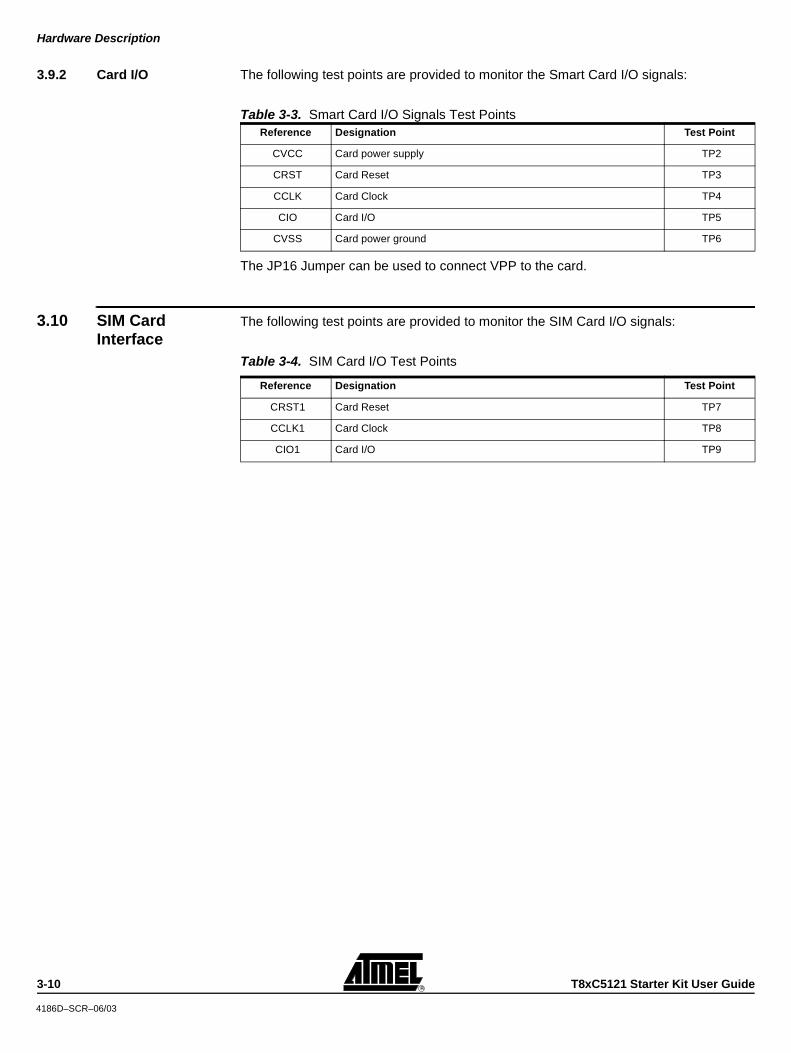
3.9.2 Card I/O The following test points are provided to monitor the Smart Card I/O signals:
Table 3-3. Smart Card I/O Signals Test Points
The JP16 Jumper can be used to connect VPP to the card.
3.10 SIM Card Interface
The following test points are provided to monitor the SIM Card I/O signals:
Table 3-4. SIM Card I/O Test Points
Reference Designation Test Point
CVCC Card power supply TP2
CRST Card Reset TP3
CCLK Card Clock TP4
CIO Card I/O TP5
CVSS Card power ground TP6
Reference Designation Test Point
CRST1 Card Reset TP7
CCLK1 Card Clock TP8
CIO1 Card I/O TP9
3-10 T8xC5121 Starter Kit User Guide
4186D–SCR–06/03
Section 4
Microcontroller Programming
The CD-ROM includes:
� The demonstration software designed to read cards
� The software tool for ISP: FLIP (Flexible In-system Programmer)
� The terminal software: Quickterm - to interface the card access on host
� The SCI library including software drivers in C language
4.1 FLIP Software FLIP is software that runs on Windows 98®, Windows NT®, XP or Windows 2000®. FLIPsupports in-system programming of Flash C51 devices through RS232. The latest ver-sion of FLIP software can be found on the Atmel web site, www.atmel.com.
4.2 Programming the T89C5121
The on-chip internal EEPROM of the T89C5121 version can be programmed usingeither:
� External EEPROM Atmel AT24C128
� Serial RS-232
4.2.1 Programming from External EEPROM Source
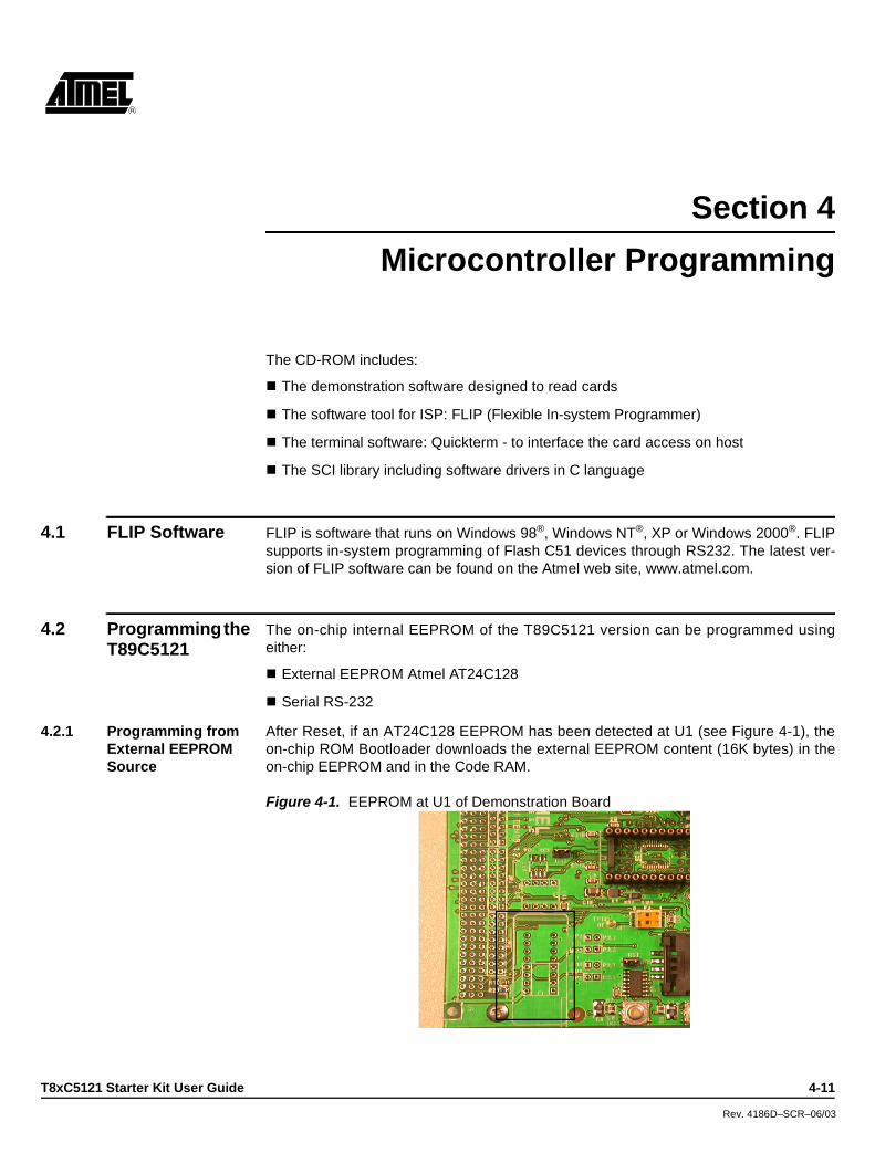
After Reset, if an AT24C128 EEPROM has been detected at U1 (see Figure 4-1), theon-chip ROM Bootloader downloads the external EEPROM content (16K bytes) in theon-chip EEPROM and in the Code RAM.
Figure 4-1. EEPROM at U1 of Demonstration Board
T8xC5121 Starter Kit User Guide 4-11
Rev. 4186D–SCR–06/03
Microcontroller Programming
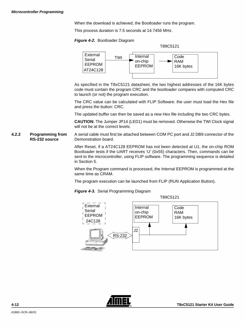
When the download is achieved, the Bootloader runs the program.
This process duration is 7.5 seconds at 14.7456 MHz.
Figure 4-2. Bootloader Diagram
As specified in the T8xC5121 datasheet, the two highest addresses of the 16K bytescode must contain the program CRC and the bootloader compares with computed CRCto launch (or not) the program execution.
The CRC value can be calculated with FLIP Software: the user must load the Hex fileand press the button: CRC.
The updated buffer can then be saved as a new Hex file including the two CRC bytes.
CAUTION: The Jumper JP14 (LED1) must be removed. Otherwise the TWI Clock signalwill not be at the correct levels.
4.2.2 Programming from RS-232 source
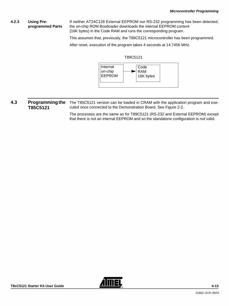
A serial cable must first be attached between COM PC port and J2 DB9 connector of theDemonstration board.
After Reset, if a AT24C128 EEPROM has not been detected at U1, the on-chip ROMBootloader tests if the UART receives ‘U’ (0x55) characters. Then, commands can besent to the microcontroller, using FLIP software. The programming sequence is detailedin Section 5.
When the Program command is processed, the Internal EEPROM is programmed at thesame time as CRAM.
The program execution can be launched from FLIP (RUN Application Button).
Figure 4-3. Serial Programming Diagram
External SerialEEPROMAT24C128
Internalon-chipEEPROM
CodeRAM16K bytes
TWI
T89C5121
External SerialEEPROM24C128
Internalon-chipEEPROM
CodeRAM16K bytes
T89C5121
RS-232J2
4-12 T8xC5121 Starter Kit User Guide
4186D–SCR–06/03
Microcontroller Programming
4.2.3 Using Pre-programmed Parts
If neither AT24C128 External EEPROM nor RS-232 programming has been detected,the on-chip ROM Bootloader downloads the internal EEPROM content (16K bytes) in the Code RAM and runs the corresponding program.
This assumes that, previously, the T89C5121 microcontroller has been programmed.
After reset, execution of the program takes 4 seconds at 14.7456 MHz.
4.3 Programming the T85C5121
The T85C5121 version can be loaded in CRAM with the application program and exe-cuted once connected to the Demonstration Board. See Figure 2-2.
The processes are the same as for T89C5121 (RS-232 and External EEPROM) exceptthat there is not an internal EEPROM and so the standalone configuration is not valid.
Internalon-chipEEPROM
CodeRAM16K bytes
T89C5121
T8xC5121 Starter Kit User Guide 4-13
4186D–SCR–06/03

Microcontroller Programming
4-14 T8xC5121 Starter Kit User Guide
4186D–SCR–06/03

Section 5
Software Description
The included demonstration software allows you to:
1. Program the microcontroller connected to the demonstration board.
2. Read data from a SmartCard or a Credit Card.
3. Display the data on the host PC (Quickterm).
The demonstration including device programming is described with ISP via RS-232communication to host.
5.1 Programming Using FLIP
This section allows you to program the microcontroller through the RS-232 cable usingFLIP software.
1. Run FLIP.
2. From the Device Menu, choose Select and select the device (T8xC5121) that is connected on your demonstration board.
T8xC5121 Starter Kit User Guide 5-15
Rev. 4186D–SCR–06/03
Software Description
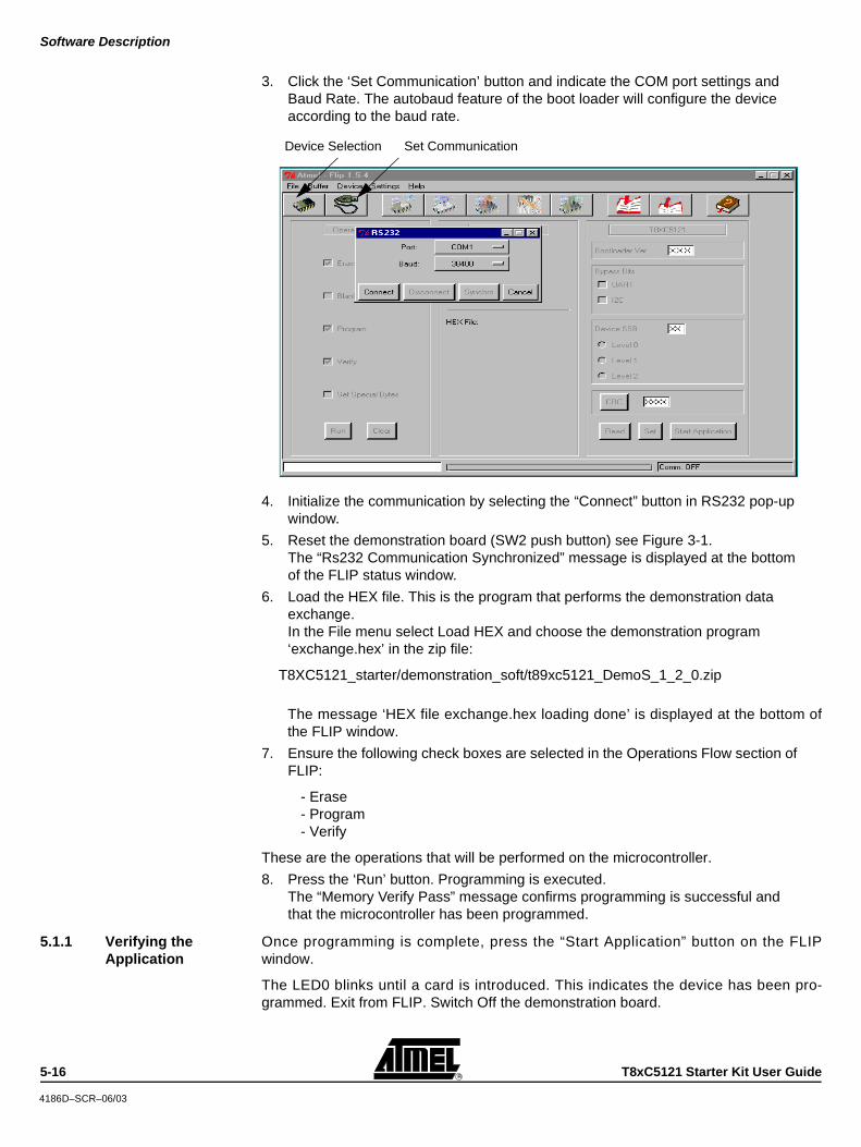
3. Click the ‘Set Communication’ button and indicate the COM port settings and Baud Rate. The autobaud feature of the boot loader will configure the device according to the baud rate.
4. Initialize the communication by selecting the “Connect” button in RS232 pop-up window.
5. Reset the demonstration board (SW2 push button) see Figure 3-1.The “Rs232 Communication Synchronized” message is displayed at the bottom of the FLIP status window.
6. Load the HEX file. This is the program that performs the demonstration data exchange. In the File menu select Load HEX and choose the demonstration program ‘exchange.hex’ in the zip file:
T8XC5121_starter/demonstration_soft/t89xc5121_DemoS_1_2_0.zip
The message ‘HEX file exchange.hex loading done’ is displayed at the bottom ofthe FLIP window.
7. Ensure the following check boxes are selected in the Operations Flow section of FLIP:
- Erase- Program- Verify
These are the operations that will be performed on the microcontroller.
8. Press the ‘Run’ button. Programming is executed. The “Memory Verify Pass” message confirms programming is successful and that the microcontroller has been programmed.
5.1.1 Verifying the Application
Once programming is complete, press the “Start Application” button on the FLIPwindow.
The LED0 blinks until a card is introduced. This indicates the device has been pro-grammed. Exit from FLIP. Switch Off the demonstration board.
Set CommunicationDevice Selection
5-16 T8xC5121 Starter Kit User Guide
4186D–SCR–06/03
Software Description
5.2 Running the Demonstration Program
5.2.1 Running Quickterm PC Software
Run Quickterm. Software is located in the zip file:
T8XC5121_starter/demonstration_soft/t89xc5121_DemoS_1_2_0.zip
1. Execute the ‘quickterm-1_0_7.exe’ file.
2. In the Quickterm File Menu, select the "Read TRM...” command and locate “whiteshark.trm” file.
3. Turn On the demonstration board.
Note: Help is available in the menu and F11 can be used to clear the display.
For the T89C5121 version, after Reset, LED0 is off during the download of programfrom EEPROM to Code RAM (4 seconds at 14.7456 MHz).
When this sequence is achieved, the program is automatically executed and the LED0blinks again while waiting for a card.
The message “Insert a card” is displayed in the Quickterm window.
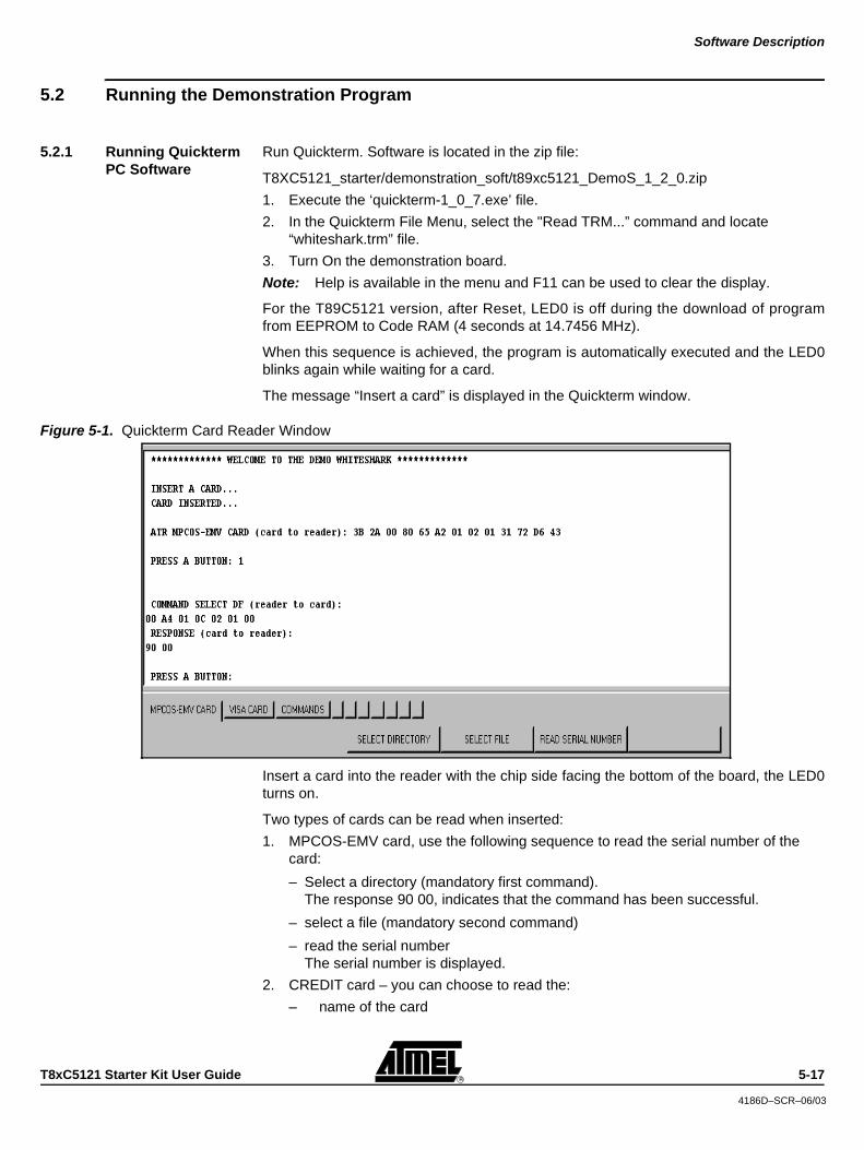
Figure 5-1. Quickterm Card Reader Window
Insert a card into the reader with the chip side facing the bottom of the board, the LED0turns on.
Two types of cards can be read when inserted:
1. MPCOS-EMV card, use the following sequence to read the serial number of the card:
– Select a directory (mandatory first command).The response 90 00, indicates that the command has been successful.
– select a file (mandatory second command)
– read the serial numberThe serial number is displayed.
2. CREDIT card – you can choose to read the:
– name of the card
T8xC5121 Starter Kit User Guide 5-17
4186D–SCR–06/03

Software Description
– end of validity of the card
– the card number
A reset of the reader occurs if the card is removed. To program the chip using a new application load a different HEX file and return to Sec-tion 5.1.
1 S
tarter Kit User Guide 5-18 T8xC5124186D–SCR–06/03
Section 6
Appendix A
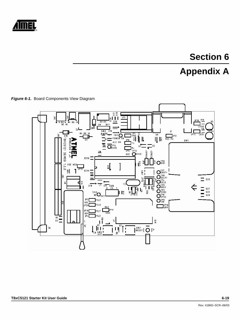
Figure 6-1. Board Components View Diagram
T8xC5121 Starter Kit User Guide
6-19Rev. 4186D–SCR–06/03
Appendix A
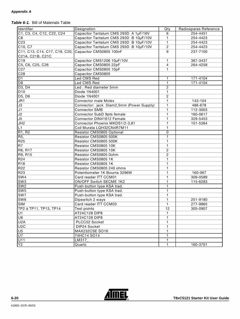
Table 6-1. Bill of Materials Table
Identifier Designation Qty Radiospares ReferenceC1, C3, C4, C12, C22, C24 Capacitor Tantalum CMS 293D A 1µF/16V 6 254-4451C8 Capacitor Tantalum CMS 293D B 10µF/10V 1 254-4423C23 Capacitor Tantalum CMS 293D B 10µF/10V 1 254-4423C10, C7 Capacitor Tantalum CMS 293D B 10µF/10V 2 254-4423C11, C13, C14, C17, C18, C20, C21A, C21B, C21C
Capacitor CMS0805 100nF 9 237-7100
C19 Capacitor CMS1206 10µF/10V 1 367-3437C5, C6, C25, C26 Capacitor CMS0805 22pF 4 264-4258C27 Capacitor CMS0805 10pF 1C28 Capacitor CMS0805D1 Led CMS Red 1 171-4104D8 Led CMS Red 1 171-4104D3, D4 Led : Red diameter 5mm 2D10 Diode 1N4001 1D5, D6 Diode 1N4001 2JR1 Connector male Molex 1 143-104J3 Connector: jack Diam2,5mm (Power Supply) 1 486-678J1 Connector SMB 1 112-3003J2 Connector SubD 9pts female 1 160-0617J5 Connector DIN41612 Female 1 329-5453JH2 Connector Phoenix MKDS1/2-3,81 1 101-5384L1 Coil Murata LQH32CN4R7M11 1R1, R2 Resistor CMS0805 Optional 0R5, Resistor CMS0805 500K 1R25 Resistor CMS0805 500K 1R7 Resistor CMS0805 10K 1R6, R17 Resistor CMS0805 10K 2R9, R15 Resistor CMS0805 0ohm 2R24 Resistor CMS0805 1K 1R18 Resistor CMS0805 1K 1R22 Resistor CMS0805 240 ohms 1R23 Potentiometer 1K Bourns 3296W 1 160-067SW4 Card reader ITT CCM01 1 309-0589SW3 ON/OFF Switch SECME 1K2 1 115-6283SW2 Push-button type KSA trad. 1SW5 Push-button type KSA trad. 1SW7 Push-button type KSA trad. 1SW6 Dipswitch 2 ways 1 251-9180SIM Card reader ITT CCM03 1 277-9865TP2 à TP11, TP13, TP14 Test points 12 305-0907U1 AT24C128 DIP8 1U6 AT24C128 DIP8 1U2A PLCC52 Socket 1U2C DIP24 Socket 1U5 MAX232CSE SO16 1U7 74HC14 SO14 1U11 LM317_ 1Y2 Quartz 1 160-3701
1 S
tarter Kit User Guide 6-20 T8xC5124186D–SCR–06/03
Appendix A
6.1 Schematics
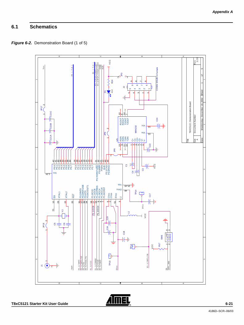
Figure 6-2. Demonstration Board (1 of 5)
5 5
4 4
3 3
2 2
1 1
DD
CC
BB
AA
P1
.3/C
C4
P1
.1/C
C8
VC
C
VC
C
VC
C
VC
C
Titl
e
Siz
eD
oc
um
ent
Num
ber
Re
v
Da
te:
She
eto
f
1.2.
0
T8
XC
51
21
De
mo
nstr
atio
nB
oard
A
15
We
dne
sda
y,D
ece
mbe
r1
8,20
02
ALE
PSEN
P2
(7:0
)P3.7/R\D\/CRST1/LED1
P3.6/W\R\/CCLK1/LED0
P0
(7:0
)/RST
P1.0/CIO
P1.5/CRST
P1.4/CCLK
P1.2/CPRES
EVcc
P3.3/INT1/OE
DVcc
Vcc
EA
P3.5/CIO1/T1
EA
ALE
P3.2/INT0
P3.4/T0
INT1_SW6
P3.3/INT1/OE
+C
19
R17
C5
+C
3
C6
JP17
12
JP3
12
J2
CO
NN
DS
UB
9-F
em
ale
11
66
22
77
33
88
44
99
55
EA
10
XT
AL1
23
XT
AL2
22
RS
T20
P3.
2/IN
T0
35
P3.
3/IN
T1/
OE
37
P3.
4/T
036
P3.
5/C
IO1/
T1
34
P1.
0/C
IO18
P1.
1/C
C8
17
P1.
2/C
PR
ES
16
P1.
3/C
C4
9
P1.
4/C
CLK
8
P1.
5/C
RS
T7
P0.
042
P0.
141
P0.
240
P0.
339
P0.
433
P0.
521
P0.
638
P0.
730
P2.
029
P2.
128
P2.
227
P2.
326
P2.
419
P2.
515
P2.
614
P2.
713
P3.
7/C
RS
T1/
RD
31
P3.
6/W
R32
PS
EN
11
ALE
/12
P3.
1/T
XD
43
P3.
0/R
XD
44
Vcc1.24
CV
cc6
CV
ss2
Vss 25,45
EV
cc51
DVcc 46
LI3
D1
C2
1A
TP14
1
C17
R24
C21
BC
21
C
+
C22
+
C1
TP13 1
Y2
U5
MA
X23
2
R1I
N13
R2I
N8
T1I
N11
T2I
N10
C+
1
C1-
3
C2+
4
C2-
5
V+
2
V-
6
R1O
UT
12
R2O
UT
9
T1O
UT
14
T2O
UT
7
Vcc 16
Vss 15
C18
L1
J1
1
2
C20
JP5
12
JP6
12
JP19
12
TP10
1
+C
24
SW
6
1 24 3
+
C4
6-21
4186D–SCR–06/03
T8xC5121 Starter Kit User Guide

Appendix A
Figure 6-3. Demonstration Board (2 of 5)
5 5
4 4
3 3
2 2
1 1
DD
CC
BB
AA
VC
C
VC
C
VC
C
VC
C
VC
C
VC
C
VC
C
Titl
e
Siz
eD
oc
um
ent
Num
ber
Re
v
Da
te:
She
eto
f
1.2.
0
T8
XC
51
21
De
mo
nstr
atio
nB
oard
A
25
We
dne
sda
y,D
ece
mbe
r1
8,20
02
External
P2.1
P2.0
Optional
Card
Reader
0
CVcc
CRST
CCLK
CIO
CVss
CIO1
CRST1
CCLK1
DVcc
Vss
SIM
Connector
CPRES
Vss
Vcc
CC4
CC8
Vpp
P3.2
P3.7
optional
optional
P3.2
P3.3/INT1/OE
JP4
12
R5
JP7
12
JP18
12
R25
+
C28
SW
4
1 2
R1
R2
AT
24C
128
A0
1
A1
2
SD
A5
SC
L6
WP
7
Vcc
8
Vss
4
C25
JP2
12
JP16
12
C26
JP23
12
C27
JP15
12
TP71
TP81
TP91
JP8
12
TP2 1
JP9
12
TP3 1
TP4 1
TP5 1
SW
7
TP61
U6
AT
24C
128
A0
1
A1
2
SD
A5
SC
L6
WP
7
Vcc
8
Vss
4
1 S
tarter Kit User Guide 6-22 T8xC5124186D–SCR–06/03

Appendix A
Figure 6-4. Demonstration Board (3 of 5)
5 5
4 4
3 3
2 2
1 1
DD
CC
BB
AA
VC
C
VC
C
DV
CC
Titl
e
Siz
eD
oc
um
ent
Num
ber
Re
v
Da
te:
She
eto
f
CA
35
We
dne
sda
y,D
ece
mbe
r1
8,20
02
Reset
INT1
LED0
LED1
LED
0
LED
1
T8XC5121
Demonstration
Board
dummy
resistor
0ohm
dummy
resistor
0ohm
RST
RST
INT1_SW6
SW
2
R15
+C
7
JP11
12
U7
B
74
HC
14
34
JP13
12
JP14
12
SW
5
U7
A
74
HC
14
12
D3 D
4
+C
8
R9
R7
R6
6-23
4186D–SCR–06/03
T8xC5121 Starter Kit User Guide
Appendix A
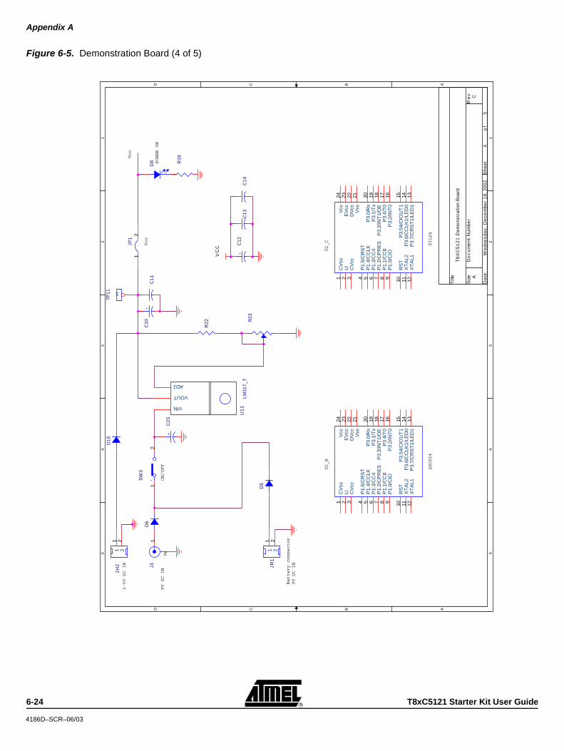
Figure 6-5. Demonstration Board (4 of 5)
5 5
4 4
3 3
2 2
1 1
DD
CC
BB
AA
VC
C
Titl
e
Siz
eD
oc
um
ent
Num
ber
Re
v
Da
te:
She
eto
f
C
T8
XC
51
21
De
mo
nstr
atio
nB
oard
A
45
We
dne
sda
y,D
ece
mbe
r1
8,20
02
9V
DC
IN
Battery
connector
Vcc
ON/OFF
SSOP24
U2_B
Vcc
POWER
ON
U2_C
DIL24
3-5V
DC
IN
9V
DC
IN
R22
+C
23
+C
10
D10
JP1
12
+C
12
JR
11
1
22
XT
AL1
12
Vcc
24
EV
cc23
DV
cc22
Vss
21
P3.
0/R
x20
P3.
1/T
x19
P3.
3/IN
T1/
OE
18
P3.
4/T
017
CV
ss1
LI2
CV
cc3
P1.
5/C
RS
T4
P1.
4/C
CLK
5
P1.
3/C
C4
6
P1.
2/C
PR
ES
7
P1.
1/C
C8
8
P1.
0/C
IO9
P3.
2/IN
T0
16
RS
T10
XT
AL2
11P
3.54
/CIO
1/T
115
P3.
6/C
CLK
1/LE
D0
14
P3.
7/C
RS
T1/
LED
113
C11
D8 R
18
D5
TP11 1
R23
J31
2
XT
AL1
12
Vcc
24
EV
cc23
DV
cc22
Vss
21
P3.
0/R
x20
P3.
1/T
x19
P3.
3/IN
T1/
OE
18
P3.
4/T
017
CV
ss1
LI2
CV
cc3
P1.
5/C
RS
T4
P1.
4/C
CLK
5
P1.
3/C
C4
6
P1.
2/C
PR
ES
7
P1.
1/C
C8
8
P1.
0/C
IO9
P3.
2/IN
T0
16
RS
T10
XT
AL2
11P
3.54
/CIO
1/T
115
P3.
6/C
CLK
1/LE
D0
14
P3.
7/C
RS
T1/
LED
113
JH
21
1
22
D6
U1
1LM
317_
T
VOUT
ADJ
VIN
SW
3
12
C13
C14
1 S
tarter Kit User Guide 6-24 T8xC5124186D–SCR–06/03

Appendix A
Figure 6-6. Demonstration Board (5 of 5)
5 5
4 4
3 3
2 2
1 1
DD
CC
BB
AA
Vcc
Titl
e
Siz
eD
oc
um
ent
Num
ber
Re
v
Da
te:
She
eto
f
C
T8
XC
51
21
De
mo
nstr
atio
nB
oard
A
55
We
dne
sda
y,D
ece
mbe
r1
8,20
02
P0
(7:0
)
P3.0
P3.1
P3.2
INT1
P3.4
T1
WR
RD
EA
ALE
RST
PSEN
Vcc
Vss
Vss
P0.7
P2.7
P2
(7:0
)
P3.2
P3.4
P3.7
P3.0
P3
(7:0
)P1.1/CC8
P1.3/CC4
P0
P2
P3
P0
(7:0
)
P3
(7:0
)
J5_A
J5_B
J5_C
P2
(7:0
)
JR2
JR3
JR41
12
23
34
45
56
67
78
8
99
1010
1111
1212
1313
1414
1515
1616
11
22
33
44
55
66
77
88
99
1010
1111
1212
1313
1414
1515
1616
11
22
33
44
55
66
77
88
99
1010
1111
1212
1313
1414
1515
1616
DIN
41
61
2fe
ma
leco
nne
ctor
1 2 3 4 5 6 7 8 9 10 11 12 13 14 15 16 17 18 19 20 21 22 23 24 25 26 27 28 29 30 31 32
DIN
41
61
2fe
ma
leco
nne
ctor
1 2 3 4 5 6 7 8 9 10 11 12 13 14 15 16 17 18 19 20 21 22 23 24 25 26 27 28 29 30 31 32
DIN
41
61
2fe
ma
leco
nne
ctor
1 2 3 4 5 6 7 8 9 10 11 12 13 14 15 16 17 18 19 20 21 22 23 24 25 26 27 28 29 30 31 32
T8xC5121 Starter Kit User Guide
6-254186D–SCR–06/03
Appendix A
6.2 References � T8XC5121 Product Datasheet.
6.3 Acronyms � ISP: In-System programming
� FLIP: FLexible In-system Programming
1 S
tarter Kit User Guide 6-26 T8xC5124186D–SCR–06/03
© Atmel Corporation 2003. All rights reserved. ATMEL® is a registered trademark of Atmel. Windows 98®,Windows NT®, and Windows 2000® are registered trademarks of Microsoft Corporation.
Disclaimer: Atmel Corporation makes no warranty for the use of its products, other than those expressly contained in the Company’s standardwarranty which is detailed in Atmel’s Terms and Conditions located on the Company’s web site. The Company assumes no responsibility for anyerrors which may appear in this document, reserves the right to change devices or specifications detailed herein at any time without notice, anddoes not make any commitment to update the information contained herein. No licenses to patents or other intellectual property of Atmel aregranted by the Company in connection with the sale of Atmel products, expressly or by implication. Atmel’s products are not authorized for useas critical components in life support devices or systems.
Atmel Headquarters Atmel Operations
Corporate Headquarters2325 Orchard ParkwaySan Jose, CA 95131TEL 1(408) 441-0311FAX 1(408) 487-2600
EuropeAtmel SarlRoute des Arsenaux 41Case Postale 80CH-1705 FribourgSwitzerlandTEL (41) 26-426-5555FAX (41) 26-426-5500
AsiaRoom 1219Chinachem Golden Plaza77 Mody Road TsimhatsuiEast KowloonHong KongTEL (852) 2721-9778FAX (852) 2722-1369
Japan9F, Tonetsu Shinkawa Bldg.1-24-8 ShinkawaChuo-ku, Tokyo 104-0033JapanTEL (81) 3-3523-3551FAX (81) 3-3523-7581
Memory2325 Orchard ParkwaySan Jose, CA 95131TEL 1(408) 441-0311FAX 1(408) 436-4314
Microcontrollers2325 Orchard ParkwaySan Jose, CA 95131TEL 1(408) 441-0311FAX 1(408) 436-4314
La ChantrerieBP 7060244306 Nantes Cedex 3, FranceTEL (33) 2-40-18-18-18FAX (33) 2-40-18-19-60
ASIC/ASSP/Smart CardsZone Industrielle13106 Rousset Cedex, FranceTEL (33) 4-42-53-60-00FAX (33) 4-42-53-60-01
1150 East Cheyenne Mtn. Blvd.Colorado Springs, CO 80906TEL 1(719) 576-3300FAX 1(719) 540-1759
Scottish Enterprise Technology ParkMaxwell BuildingEast Kilbride G75 0QR, Scotland TEL (44) 1355-803-000FAX (44) 1355-242-743
RF/AutomotiveTheresienstrasse 2Postfach 353574025 Heilbronn, GermanyTEL (49) 71-31-67-0FAX (49) 71-31-67-2340
1150 East Cheyenne Mtn. Blvd.Colorado Springs, CO 80906TEL 1(719) 576-3300FAX 1(719) 540-1759
Biometrics/Imaging/Hi-Rel MPU/High Speed Converters/RF Data-com
Avenue de RochepleineBP 12338521 Saint-Egreve Cedex, FranceTEL (33) 4-76-58-30-00FAX (33) 4-76-58-34-80
Web Sitehttp://www.atmel.com
Printed on recycled paper.
41
86D–SCR–06/03 /xMOther terms and product names may be the trademarks of others.