table of contents 2014 ieee photovoltaic s ...eds.ieee.org/images/files/newsletters/newsletter...
TRANSCRIPT
We invite you to join us for the 40th IEEE Photovoltaic Specialists
Conference (PVSC), being held June 8–13, 2014, in Denver, Colorado.
Since our first meeting in 1961, the PVSC has established itself as the
world’s leading technical event for scientists, engineers and decision-
makers across the full spectrum of PV technologies.
As PV technologies continue to leap forward at an unprecedent-
ed pace, we are expecting yet another tremendous conference.
Here are just some of the highlights to come.
40th IEEE PVSC Highlights
TutorialsAs always, the week will begin with a series of educational ses-
sions on PV technologies and markets. These half-day tutorials will
offer valuable insights for everyone from industry newcomers who
may appreciate the “Photovoltaics 101” sessions, to veterans look-
ing to expand their understanding in new areas, such as Si experts
JANUARY 2014 VOL. 21, NO. 1 ISSN: 1074 1879 EDITOR-IN-CHIEF: M.K. RADHAKRISHNAN
TABLE OF CONTENTS
BoG Meeting Recap and New EDS President Elect! . . . . . . . . . . . . . 1
Upcoming Technical Meetings . . . . . . . . . . . . . 3
Society News . . . . . . . . . . . . . . . . . . . . . . . . . . . 9
Regional and Chapter News . . . . . . . . . . . . . . 21
EDS Meetings Calendar . . . . . . . . . . . . . . . . . 34
2014 IEEE PHOTOVOLTAIC SPECIALISTS CONFERENCE (PVSC)
The EDS Board of Governors (BoG) meeting
series was held in conjunction with the 2013 In-
ternational Electron Devices Meeting (IEDM) in
Washington, DC. The BoG series was particularly
spirited this year, with over a dozen committee
and ancillary meetings taking place during the
weekend of December 6–8.
EDS is blessed with a diverse and engaged
volunteer corps charged with stewarding the
society’s vital interests in all areas of our opera-
tions: conferences, publications, membership en-
gagement, technical activities and education. The
BoG meeting was especially lively this year, with
over 20 volunteers presenting.
Among the major actions taken was the BoG
approval of revisions to the EDS Constitution and
Bylaws. Led by an Ad-hoc committee comprised
of BoG members Simon Deleonibus (Chair), Cor
Claeys, Jacobus Swart, and Zeynep Celik-Butler,
and with assistance from Irv Engelson, the chang-
es to EDS’s governing documents will provide
better consistency, transparency, and flexibility
into EDS’s structure and operations. The revised
BOG MEETING RECAP AND NEW EDS
PRESIDENT ELECT!
(continued on page 8)
(continued on back cover)
RIC
H G
RA
NT
AN
D V
ISIT
DE
NV
ER
YOUR COMMENTS SOLICITEDYour comments are most welcome. Please write directly to the
Editor-in-Chief of the Newsletter at [email protected]
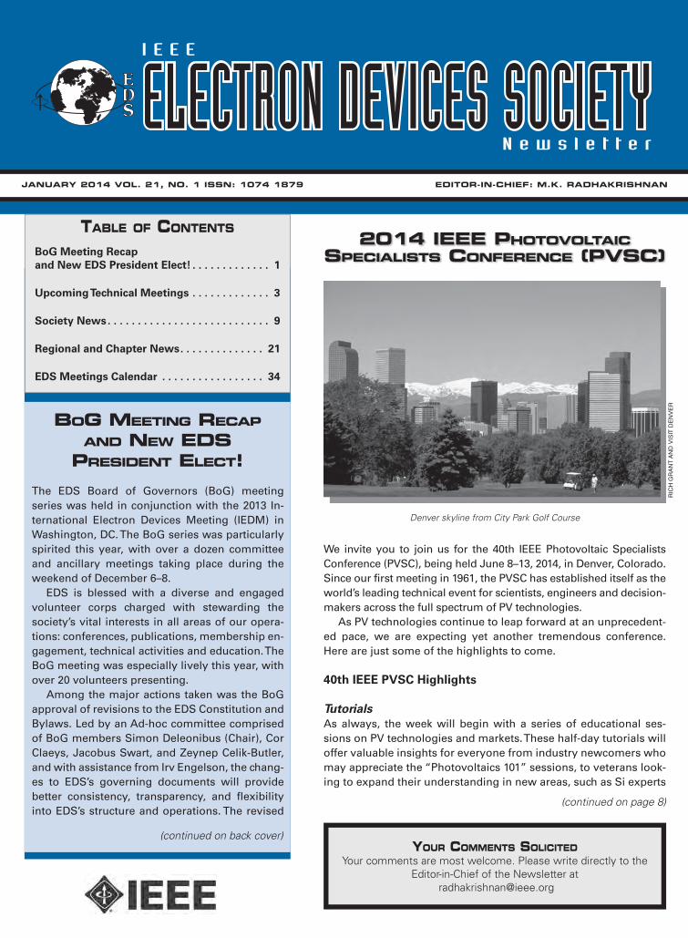
Denver skyline from City Park Golf Course

2 IEEE Electron Devices Society Newsletter ❍ January 2014
ELECTRON DEVICES
SOCIETY
NEWSLETTER
EDITORIAL STAFF
PresidentAlbert Z.H. WangUniversity of California, RiversideE-mail: [email protected]
President-Elect Samar SahaUltrasolar TechnologyE-mail: [email protected]
TreasurerRavi M. TodiQualcomm Technologies, Inc.E-mail: [email protected]
SecretaryFernando GuarinIBM MicroelectronicsE-mail: [email protected]
Jr. Past PresidentPaul K.L. YuUniversity of California at San DiegoE-mail: [email protected]
Sr. Past PresidentRenuka P. JindalUniversity of Louisiana atLafayetteE-mail: [email protected]
Vice President of Membership and ServicesMikael OstlingKTH, Royal Institute of TechnologyE-mail: [email protected]
Vice President of Publications and ProductsBin Zhao Fairchild SemiconductorE-mail: [email protected]
Vice-President of Regions/ChaptersXing ZhouNanyang Technological University E-mail: [email protected]
Vice President of Technical Committees & MeetingsLeda LunardiNorth Carolina State UniversityE-mail: [email protected]
IEEE NewslettersTheresa SmithIEEE Operations CenterE-mail: [email protected]
Executive DirectorChristopher JannuzziIEEE Operations CenterE-mail: [email protected]
Membership AdministratorJoyce LombardiniIEEE Operations CenterE-mail: [email protected]
IEEE Electron Devices Society Newsletter (ISSN 1074 1879) is published quarterly by the Electron Devices Society of the Institute of Electrical and Electronics Engineers, Inc. Headquarters: 3 Park Avenue, 17th Floor, New York, NY 10016-5997. Printed in the U.S.A. One dollar ($1.00) per member per year is included in the Society fee for each member of the Electron Devices Society. Periodicals postage paid at New York, NY and at additional mailing offices. Postmaster: Send address changes to IEEE Electron Devices Society Newsletter, IEEE, 445 Hoes Lane, Piscataway, NJ 08854.
Copyright © 2014 by IEEE: Information contained in this Newsletter may be copied without permission provided that copies are not used or distributed for direct commercial advantage, and the title of the publication and its date appear on each photocopy.
Editor-In-ChiefM.K. RadhakrishnanNanoRelE-mail: [email protected]
REGIONS 1-6, 7 & 9Eastern, Northeastern & South-eastern USA (Regions 1,2 & 3)Fernando GuarinIBM MicroelectronicsE-mail: [email protected]
Central USA & Canada(Regions 4 & 7)Peyman ServatiUniversity of British ColumbiaE-mail: [email protected]
Southwestern & Western USA(Regions 5 & 6)Adam M. ConwayLawrence Livermore Nat. Lab.E-mail: [email protected]
Latin America (Region 9)Francisco J. Garcia SanchezUniversity Simon BolivarE-mail: [email protected]
REGION 8Eastern Europe & the former Soviet UnionTomislav SuligojUniversity of ZagrebE-mail: [email protected]
Scandinavia & Central EuropeZygmunt CiotaTechnical University of LodzE-mail: [email protected]
UK, Middle East & AfricaJonathan TerryThe University of EdinburghE-mail: [email protected]
Western EuropeJan VobeckyAbb Switzerland Ltd.E-mail: [email protected]
REGION 10Australia, New Zealand & South AsiaM.K. RadhakrishnanNanoRelE-mail: [email protected]
Northeast AsiaKuniyuki KakushimaTokyo Institute of TechnologyE-mail: [email protected]
East AsiaMansun J. ChanHong Kong Univ. of Sc. & Tech.E-mail: [email protected]
CONTRIBUTIONS WELCOME
Readers are encouraged to submit news items concerning the Society and its members. Please send your ideas/articles directly to either the Editor-in-Chief or appropriate Editor. The e-mail addresses of these individuals are listed on this page. Whenever possible, e-mail is the preferred form of submission. NEWSLETTER DEADLINES
ISSUE DUE DATE
January October 1st April January 1st July April 1st October July 1st
The EDS Newsletter archive can be found on the Society web site at http://eds.ieee.org/eds-newsletters.html. The archive contains issues from July 1994 to the present.
EDS Board of Governors (BoG)Elected Members-at-Large
Elected for a three-year term (maximum two terms) with ‘full’ voting privileges
2014 TERM 2015 TERM 2016 TERM
Z. Celik-Butler (1) Daniel Camacho (1) A. Escobosa (2)M. Chan (1) Subramanian S. Iyer (2) Ru Huang (1)S. Chung (1) Meyya Meyyappan (2) Leda Lunardi (1)S. Deleonibus (2) Arokia Nathan (2) M. Ostling (2)F. Guarin (2) Michael Shur (2) M.K. Radhakrishnan (2)T.L. Ren (1) Doug Verret (1) Jacobus Swart (1)S. Saha (2) Bin Zhao (2) X. Zhou (2)E. Sangiorgi (1)
IEEE prohibits discrimination, harassment, and bullying. For more information, visit http://www.ieee.org/web/aboutus/whatis/policies/p9-26.html.
Forestry logo

January 2014 ❍ IEEE Electron Devices Society Newsletter 3
2014 IEEE INTERNATIONAL VACUUM ELECTRONICS CONFERENCE (IVEC)
U P C O M I N G T E C H N I C A L M E E T I N G S
We are pleased to announce that
the Fifteenth International Vacuum
Electronics Conference (IVEC 2014)
will be held April 22–24, 2014, at the
Portola Hotel & Spa in Monterey,
California. Visitors from around the
world come to Monterey to experi-
ence its natural coastal beauty, visit
the renowned Monterey Bay Aquar-
ium, and experience its rich historic
past memorialized in the novels of
John Steinbeck.
With technical co-sponsorship
from the IEEE Electron Devices So-
ciety, the conference will provide a
forum for scientists and engineers
from around the globe to present
the latest developments in vacuum
electronics technology at frequen-
cies ranging from the UHF to THz
bands.
IVEC was originally created in
2000 by merging the U.S. Power
Tubes Conferences and the Euro-
pean Space Agency TWTA Work-
shops. Now a fully international
conference, IVEC is held every oth-
er year in the U.S., and in Europe
and Asia alternately every fourth
year. After the successful and en-
joyable meeting in Paris, France
in May, IVEC 2014 will return to its
beautiful U.S. location in the city of
Monterey.
Plenary talks will provide insights
into the history, the broad spectrum
of fundamental physics, the scien-
tific issues, and the technological
applications driving the current di-
rections in vacuum electronics re-
search. Technical presentations will
range from the fundamental phys-
ics of electron emission and modu-
lated electron beams to the design
and operation of devices at UHF to
THz frequencies, theory and com-
putational tool development, active
and passive components, systems,
and supporting technologies. Sys-
tem developers will find that IVEC
provides a unique snapshot of the
current state-of-the-art in vacuum
electron devices. These devices
continue to provide unmatched
power and performance for ad-
vanced electromagnetic systems,
particularly in the challenging fre-
quency regimes of millimeter-wave
and THz electronics.
The John R. Pierce Award for
Excellence in Vacuum Electronics
and a Student Paper Award will be
presented at the conference. As in
past conferences, the meeting and
social events will provide unique
opportunities to renew or establish
new friendships with colleagues, in-
teract with customers and end-users,
and meet students and academic
researchers.
The conference website is the
best source of information about
IVEC 2014, including Technical Ar-
eas, Paper Submission, Registration,
Accommodation, and other impor-
tant dates and events. Please visit
http://ivec2014.org/. To enquire about
exhibitor space and conference
support, contact Alicia Waldron, Pali-
sades Convention Management
(212-460-8090 ext. 216, awaldron@
pcm411.cm).
You also can learn more about IVEC
by visiting http://vacuumelectronics.
org/, the EDS Vacuum Electronics
Technical Committee website.
We look forward to seeing you in
Monterey!
Da vid K. Abe
2014 IVEC General Chair
U.S. Naval Research Laboratory
Washington, DC, USA
4 IEEE Electron Devices Society Newsletter ❍ January 2014
2014 IEEE INTERNATIONAL RELIABILITY PHYSICS SYMPOSIUM (IRPS)
The IEEE I nternational Reliabil-
ity Physics Symposium (IRPS) is the
world’s premier forum for leading-
edge research addressing devel-
opments in the Reliability Physics
of devices, materials, circuits, and
products. IRPS is the conference
where emerging Reliability Physics
challenges and possible solutions to
achieve realistic End-of-Life projec-
tions are first discussed. This year,
the IRPS will be held at Hilton Waiko-
loa Village, Waikoloa, HI, U.S.A.
Scheduled for June 1–5, 2014, the
IRPS will commence with two full
days of tutorials and year-in-review
on Sunday, June 1st and Monday,
June 2nd.
The IRPS draws presentations
and attendees from industry, aca-
demia and governmental agencies
worldwide. No other meeting pres-
ents as much leading work in so
many different areas of reliability of
electronic devices, encompassing
silicon device, non-silicon device,
process technology, nanotechnol-
ogy, optoelectronics, photovoltaic
and MEMS technology.
For the IRPS 2014, we are empha-
sizing Electronic Systems reliability
with sub-topics in consumer elec-
tronics reliability and design-for-reli-
ability. We are also emphasizing chip-
package interactions and advanced
packaging reliability concerns.
IRPS 2014 will also feature in-
creased participation in the fields of
Advanced CMOS scaling, GaN, new
materials introduction, new processes
or integration strategies, and/or funda-
mentally new device architectures. The
conference will offer a full slate of tuto-
rials, evening panel debates and work-
shops, invited plenary talks in addition
to an outstanding technical program.
The hotel is located in Waiko-
loa Village on the Island of Hawaii
(known as The Big Island). It has
a wide variety of resort activities
to choose from and is the perfect
starting point to explore Hawaii Is-
land, the Island of Adventure. At the
Waikoloa resort, there are endless
opportunities including interactive
dolphin encounters, snorkeling, kay-
aking, and standup paddle boarding.
Also, there are two championship
golf courses within the Waikoloa
Beach Resort. Several guided tours
to Volcano National Park, Mauna Kea
summit and Waipio Valley are avail-
able. You can view the video of the
resort on IRPS website www.irps.org
IRPS consists of three days ( Tues–
Thurs, June 3–5) of plenary and par-
allel technical sessions presenting
original, state-of-the-art work.
Other opportunities at the sympo-
sium include:
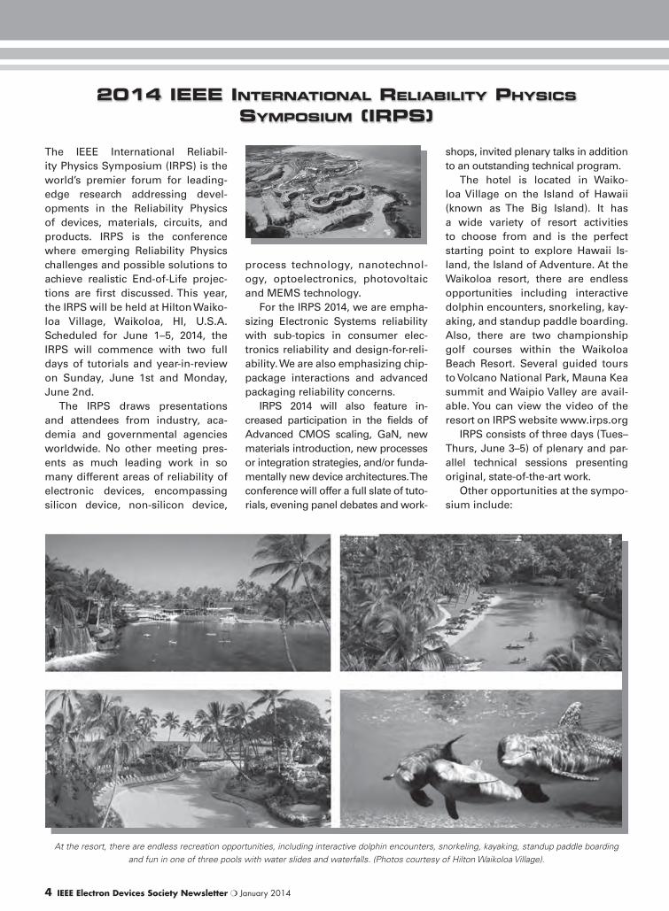
At the resort, there are endless recreation opportunities, including interactive dolphin encounters, snorkeling, kayaking, standup paddle boarding and fun in one of three pools with water slides and waterfalls. (Photos courtesy of Hilton Waikoloa Village).
January 2014 ❍ IEEE Electron Devices Society Newsletter 5
• Two-Day Tutorial Program (Sun-
day–Monday, June 1–2). The IRPS
tutorial program is a comprehen-
sive two-day event designed to
help both the new engineer and
experienced researcher. The tu-
torial program contains both be-
ginner and expert tracks, and is
broken down into topic areas
that allow the attendee to partic-
ipate in tutorials relevant to their
work with a minimum of conflicts
between subject areas.
• Year in Review Session (Monday,
June 2). These seminars provide
a summary of the most signifi-
cant developments in the reliabil-
ity community over the past year.
This serves as a convenient, sin-
gle source of information for
attendees to keep current with the
recent reliability literature.
Industry experts serve as the
“tour guide” and save you time
by collecting and summarizing
this information to bring you up
to date in a particular area as
efficiently as possible.
• Poster Session will provide an
additional opportunity for au-
thors to present their original
research. The setting is informal
and allows for easy discussion
between authors and other
attendees.
• Panel Discussion and Workshop Sessions enhance the sympo-
sium by providing the attend-
ees an opportunity to hear the
thoughts and opinions of indus-
try experts and meet in informal
groups to discuss key reliabili-
ty physics topics with the guid-
ance of experienced moderators.
Some of the workshop topics are
directly coupled to the technical
program to provide a venue for
more discussion on the topic.
• Vendor Exhibits. Held in paral-
lel with the technical sessions,
the equipment demonstrations
provide a forum for manufac-
turers of state-of-the-art labora-
tory equipment to present their
products. Attendees are encour-
aged to visit the manufacturers’
booths for information and
demonstrations.
• IRPS Paper Awards. IRPS be-
stows awards for Best Paper,
Outstanding Paper, Best Poster
and Best Student Talk. The Best
Paper author is typically invited
to present the paper at ESREF in
October.
For registration and other infor-
mation, visit the IRPS 2014 home
page at http://www.irps.org/ .
The IRPS committee members
look forward to seeing you in June.
Charles Slayman
2014 IRPS Publicity Chair
Cisco Systems
Prasad Chaparala
2014 IRPS General Chair
Alta Devices
2014 IEEE INTERNATIONAL INTERCONNECT TECHNOLOGY CONFERENCE (IITC)/ADVANCED
METALLIZATION CONFERENCE (AMC)The 17th annual IITC conference will
be held May 21–23, 2014, in conjunc-
tion with the 31st Advanced Metalli-
zation Conference at the DoubleTree
Hotel in San Jose, California. It will
be preceded by a day-long workshop
on “Manufacturing of Intercon-
nect Technologies: Where are we
now and where do we go from
here?” on Tuesday, May 20th. The
conference attracts professionals
from industry, academia, and na-
tional laboratories in semiconduc-
tor processing, interconnect design,
and equipment development.
Recognizing the industry’s need
to look at disruptive interconnect
solutions in the long term, the con-
ference will feature sessions dedi-
cated to advanced materials, such
as carbon-based interconnects,
atomic layer deposited dielectrics
and atomic layer deposited metals.
Other important topics for IITC/AMC
2014 include dielectric reliability, 3D
integration as well as design and ar-
chitectural solutions to interconnect
challenges.
IITC/AMC 2014 continues to ad-
dress fundamental interconnect per-
formance issues, with presentations
in the areas of process integration
(for logic and/or memory); reliability;
advanced interconnects and systems
interconnections; through-silicon vias
and 3D integration; packaging; nov-
el materials and concepts; process
modeling, and all back-end materials
and unit processes associated with
interconnect technology, including in-
depth explorations of related manu-
facturing issues.
The IITC rotates its location be-
tween Asia, the US, and Europe. In
2013, IITC was held in Kyoto, Japan.
In 2012, IITC was held in San Jose.
The 2015 IITC will be held in Europe.
Oral and poster presentations at
IITC/AMC 2014 will include the fol-
lowing topics:
Materials and Unit Processes • Dielectric materials and associat-
ed deposition
• Metal deposition, planarization and
patterning processes/equipment
• Novel or improved tools for inter-
connect metrology
Novel Materials and Concepts• Carbon based interconnects,
including vias and interconnects
composed of carbon nanotubes
or grapheme
• Optical interconnects and RF
interconnects

6 IEEE Electron Devices Society Newsletter ❍ January 2014
3D Integration• Through silicon via (TSV) materi-
als, process integration, reliabili-
ty, interactions with packaging
• 3D packaging schemes
• Circuits and architecture for 3D
integration
Process Integration and Chip Package Interactions• Multilevel interconnect process-
es, novel interconnect structures,
contact/via integration, metal bar-
rier and materials interface issues
• Integration processes and issues
specific to logic or memory
• Novel non-volatile, interconnect
embedded memories
Process Modeling• CMP, metal/dielectric deposition
and etching processes
Reliability • Metal electromigration and stress
voiding, dielectric integrity, ther-
mal effects, passivation issues,
interconnect reliability prediction/
modeling.
Memory Materials in the Interconnect• Memory Materials like Phase
Change Memory (PCM), Resistive
RAM (RRAM), Conductive Bridge
RAM (CB-RAM) and Magnetore-
sistive RAM (MRAM)
Interconnect Systems • Interconnect performance mod-
eling and high frequency charac-
terization
• Interconnect system integration,
novel architectures and advanced
interconnect concepts
• Circuit techniques to improve
interconnects
Novel Systems and Packaging• Wafer-level packaging schemes
• Packaging of optical intercon-
nects, RF, and SoC
Contacts and Front-end Metallization• Salicides, replacement gate
processes, local interconnects
Supplier Exhibits and SeminarsSupplier exhibits and seminars
are included as an integral part of
the IITC/AMC technical program.
Held on the first and second days
of the conference, the supplier
seminars offer additional learn-
ing and networking opportunities,
and provide alternative forums to
address specific technological chal-
lenges.
The IITC conference website is
http://www.ieee.org/conference/iitc.
For additional information and in-
quiries regarding supplier exhibits
and seminars, please contact Noel
Russell, Sponsorship Chair at Noel.
General Co-Chairs of
IITC/AMC 2014
Deepak C. Sekar, Rambus Labs
Eric Eisenbraun, SUNY CNSE
Zsolt Tokei, IMEC
Hyun-Chul Sohn, Yonsei University
Noel Russell, TEL
2014 IEEE SYMPOSIA ON VLSI TECHNOLOGY AND CIRCUITS
LATEST DEVELOPMENTS IN MICROELECTRONIC TECHNOLOGY TO BE FEATURED AT THE 2014 SYMPOSIA ON VLSI TECHNOLOGY AND CIRCUITS
JOINT VLSI TECHNOLOGY AND CIRCUITS FOCUS SESSIONS INCLUDE ADVANCED MEMORY TECHNOLOGIES, 3D TSV INTEGRATION, AND THE IMPACT OF SCALING ON ADVANCED DEVICE DESIG...
The 2014 Symposia on VLSI Technol-
ogy and Circuits will be held at the
Hilton Hawaiian Village June 9–12,
2014 (Technology) and June 10–13,
2014 (Circuits). Linked for the past 26
years, the annual Symposia on VLSI
Technology and Circuits provide the
opportunity for the world’s top de-
vice technologists, circuit and system
designers to engage in an open ex-
change of leading edge ideas at the
world’s premier mid-year conference
for microelectronic technology. Since
1987, the Symposia on VLSI Technol-
ogy and Circuits have been held to-
gether, alternating each year between
sites in the US and Japan, making it
possible for attendees to learn about
new directions in the development of
VLSI technology and circuit design
through some of the industry’s lead-
ing research and development work.
The comprehensive technical pro -
grams at the two Symposia are
DO
UB
LET
RE
E B
Y H
ILTO
N
January 2014 ❍ IEEE Electron Devices Society Newsletter 7
augmented with short courses, invited
speakers and several evening rump
sessions. As a new highlight, the Sym-
posia have introduced joint technol-
ogy and circuit focus sessions in 2012,
consisting of invited and contributed
papers on topics of mutual interest to
attendees.
The Symposium on VLSI Tech-
nology program will focus on break-
throughs in devices and processes
including:
• Memory, logic, RF, analog,
mixed-signal, I/O, high-voltage,
imaging, and MEMS
• Advanced gate stacks, channels, junc -
tions, contacts and interconnects
• Heterogeneous integration of
non-Si materials/substrates on
Si substrates
• Advanced lithography and high-
density VLSI patterning technologies
• Beyond-CMOS functional devices
with a path for VLSI implemen-
tation
• Packaging technologies, through-
silicon-vias (TSVs) and 3D-sys-
tem integration
• Advanced materials, device anal-
ysis, and modeling
• Theoretical understanding, oper-
ation fundamentals and reliabil-
ity issues related to the above
devices
• VLSI manufacturing concepts
and technologies
The Symposium on VLSI
Circuits program will showcase
innovations and advances in the
following areas:
• Digital circuits and processor
techniques, including circuits and
techniques for standalone and
embedded processors
• Memory circuits, architectures,
and interfaces for volatile and
non-volatile memories, including
emerging memories
• Clock generation and distribution
for high-frequency digital and
mixed-signal applications
• Analog and mixed-signal cir-
cuits, including data converters,
sensor interface circuits, and
amplifiers
• Wireline receivers and transmit-
ters, including circuits for inter-
chip and long-reach applications
• Wireless receivers and transmit-
ters, including circuits for WAN,
LAN, PAN, BAN, and inter-chip
applications
• Power management circuits, in-
cluding battery management
circuits, voltage regulators, en-
ergy harvesting circuits, and
circuits for renewable energy
applications
• Application-oriented circuits and
VLSI systems, including biomed-
ical applications, and including
SoC and SiP architectures and
implementations
Joint technology and circuits
focus sessions will feature invited
and contributed papers highlighting
major innovations and advances in
materials, processes, devices, inte-
gration, reliability and modeling in
the following areas of joint interest:
• Design in scaled technologies:
Impact of advanced devices,
structures, materials and inter-
connects on digital circuit perfor-
mance, power, density; device
design & process/technology
optimization for analog/mixed-
signal circuits
• Design enablement: Technology
and design co-optimization for
improved performance, yield, re-
liability, ultra-low voltage/power
operation, density, and cost
• Memory technologies: Discrete
and embedded SRAM, DRAM
and NVRAM technology/design
co-optimization
• 3D-integration (TSV): 3D-tech-
nologies and system co-opti-
mization; power delivery and
management; thermal manage-
ment; inter-chip communications
Best Student Paper AwardBased on the quality of the papers
and presentations, an award for
best student paper at the Sympo-
sia will be chosen, and the recipient
will receive a financial prize, travel
cost support and a certificate at the
opening session of the 2015 Sympo-
sium. For a paper to be reviewed
for this award, the author must be
enrolled as a full-time student at
the time of submission, must be the
lead author and presenter of the pa-
per, and must indicate on the web
submission form that the paper is a
student paper.
Paper Submission DeadlineThe deadline for paper submissions
to both conferences is January 27,
2014. Late-news deadline for the
Symposium on VLSI Technology is
March 27, 2014; there is no late-news
submission for the Symposium on
VLSI Circuits. Complete details for
paper submission can be found on-
line at: http://www.vlsisymposium.
org/authors/.
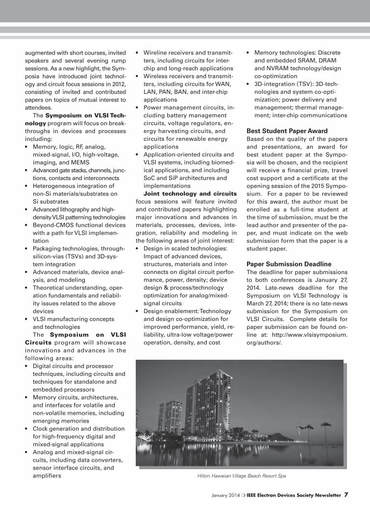
Hilton Hawaiian Village Beach Resort Spa
8 IEEE Electron Devices Society Newsletter ❍ January 2014
(continued from page 1)
2014 IEEE PHOTOVOLTAIC SPECIALISTS CONFERENCE (PVSC)
looking to learn how a multi-junction
solar cell works. These courses will
provide a focused, rapid education
in a range of topics of interest to the
PV community.
Technical ProgramAbove all, the PVSC is renowned for
its one-of-a-kind technical program,
where the world’s leading voices in
PV present their latest findings and
offer forward-looking insights on
the future of the industry. For the
40th meeting, we are expecting over
1,000 submissions, which will bring
you an unparalleled educational ex-
perience across 12 topical areas:
Area 1. Fundamentals and New
Concepts for Future Technologies
Area 2. Thin Film Polycrystalline
Photovoltaics
Area 3. III-V and Concentrator
Technologies
Area 4. Crystalline Silicon Photo-
voltaics
Area 5. Thin Film Silicon Based PV
Technologies
Area 6. Organic Photovoltaics
Area 7. Space Technologies
Area 8. Characterization Methods
Area 9. PV Modules and Manufac-
turing
Area 10. PV Systems and Applica-
tions
Area 11. PV Deployment
Area 12. PV Reliability
As you can see, our technology
focus spans from the basic technolo-
gies through system development
and characterization, to deploy-
ment. Area 7 is one to highlight, as
the PVSC is the only PV technology
conference that maintains a focus
of space technologies, which is the
birthplace of PV for electric energy
generation and continues as the in-
cubator for high efficiency technolo-
gies. Areas 9 through 12 form our
PV system development and deploy-
ment thrust in which we track the
transition of PV technologies from
development to use in the field and
analyze the on-station performance.
With this line up of topical areas, the
technology that you are developing
or interested in learning about (or
both!) will be sure to find a home at
the PVSC.
The PVSC Exhibit hall will be pro-
viding an action-packed floorshow
with an extensive list of companies
eager to interface with the PV spe-
cialists at the conference. The theme
for our exhibits is tools for the PV
specialist. Being the premier techni-
cal PV conference, the exhibiters will
be those serving the needs of the
PV specialist, displaying the latest
in solar simulator capability, electri-
cal material characterization, semi-
conductor growth tools, and many
more. Our exhibit hall will resemble
a toy store for the child in all of our
PV specialists.
Our student program is worth
noting, as the PVSC endeavors to
foster as much student participation
as possible. We facilitate access to
the conference with a reduced stu-
dent registration rate, and the grad-
uate student assistant program, and
we strive to enhance the student’s
conference experience with events
like our student mixer and the best
student paper award. We also main-
tain our PV Jobs portal, which is of
keen interest to our students and to
our community as a whole.
So, as you can see, the IEEE PVSC
40 is shaping up to be our most ex-
citing conference yet, so be on the
look-out for our First Call for Papers
and mark your calendar for the ab-
stract submission deadline of Febru-
ary 10, 2014 and the conference date
of June 8–13, 2014.
Rebekah Feist
2014 PVSC Publicity Chair
Dow Chemical
Saginaw, MI, USA
Sponsoring OrganizationsThe Symposium on VLSI Technol-
ogy is sponsored by the IEEE Elec-
tron Devices Society and the Japan
Society of Applied Physics, in coop-
eration with the IEEE Solid-State Cir-
cuits Society.
The Symposium on VLSI Circuits
is sponsored by the IEEE Solid-State
Circuits Society and the Japan Soci-
ety of Applied Physics, in cooperation
with the Institute of Electronics, In-
formation and Communication Engi-
neers and the IEEE Electron Devices
Society.
Further Information, Registration
and Official Call for Papers: http://
www.vlsisymposium.org.
Chorng-Ping Chang
2014 Publicity Chair
Symposium on VLSI Technology
Applied Materials, Inc.
Gunther Lehmann
2014 Publicity Chair
Symposium on VLSI Circuits
Infineon Technologies AG

January 2014 ❍ IEEE Electron Devices Society Newsletter 9
S O C I E T Y N E W S
EDS INCOMING PRESIDENT’S MESSAGE
Dear Fellow EDS
Friends,
I am honored
to write to you as
the new EDS Pres-
ident. For about
twenty years, EDS
has been helping
me in my career
training, develop-
ment and tran-
sition. Now, it is the time for me to
take the leading role as the dedicat-
ed, enthusiastic and chief volunteer,
my definition for the EDS President,
to promote the EDS vision, execute
the EDS mission, and serve the EDS
community.
With about 10,000 members and
about 174 chapters around the globe,
EDS has been contributing critically
to advancing the human society
since 1952 by continuously develop-
ing and delivering various “electron
devices,” which are the foundation
elements of modern information
technologies. Looking forward, EDS
will continue to play the key role to
benefit the human society.
I believe that EDS must be more
flexible and adaptive to the rapid-
changing field with quick and early
involvement in emerging technolo-
gies. I believe that EDS must con-
tinue its globalization efforts by
penetrating the emerging regions
aggressively while holding our exist-
ing grounds. I believe that EDS must
continuously attract volunteers by
member involvement and recogni-
tion. I believe that EDS must develop
and deliver meaningful products to
address its member needs in career
enhancement and transition. As the
EDS President, I promise to work
diligently to promote the EDS values
and serve the EDS community.
I would like to express my sincer-
est appreciation to my predecessor,
Paul Yu, and the retiring ExCom team
for their hard work during the past
two years.
Looking ahead, there are opportu-
nities and challenges for EDS. As the
chief volunteer, I will work closely
with all of you to make sure that EDS
will become better and contribute
more to the well-being of humanity.
Albert Wang
EDS President
University of California,
Riverside, CA, USA
Albert WangEDS President
2014–2015
EDS OUTGOING PRESIDENT’S MESSAGE
Dear All,
It’s been said
that the days are
long and the years
are short.
Looking back
at my tenure as
EDS president, I
remember many
such days (and
nights) travelling
around the world, working late into
the night with our dedicated volun-
teers and staff, to advance the vision
and mission of EDS. Yet somehow
it’s hard to fathom that my time as
President of this wonderful society
has, in seems like the blink of eye,
come to pass.
In my previous message I spoke
of our major accomplishments and
new initiatives now underway, in-
cluding our General Election pilot
and the establishment of the EDS
Mission Fund. But in this message,
I want to focus on something more
important than the work of EDS…
and that’s the volunteers and mem-
bers of EDS.
When I think of the amazing
people I have worked with in these
past two years, I am humbled and
honored to have served as your
President. I want to take a moment
to thank you all for this opportunity
and for allowing me to share in the
stewardship of the Electron Devices
Society. The list of people to thank is
far too long to mention everyone as
there are literally hundreds of volun-
teers without whom the successes
of my presidency would not be pos-
sible. That being said, I do owe a spe-
cial debt of gratitude to the following
EDS volunteers:
The EDS Executive Committee—
President Elect, Albert Z.H. Wang; Sr.
Past President, Cor L. Claeys; Jr. Past
President, Renuka P. Jindal; Secretary,
Fernando Guarin; Treasurer, Ravi M.
Todi; Vice President of Awards, Mar-
vin H. White; Vice President of Educa-
tional Activities, Meyya Meyyappan;
Vice President of Meetings, Bin Zhao;
Vice President of Membership, Jamal
Deen; Vice President of Publications,
Samar K. Saha; Vice President of Re-
gions & Chapters, Xing Zhou; and
Vice President of Technical Activities,
Joachim N. Burghartz.
Elected Members-at Large—Arturo
Escobosa, Juin J. Liou, Mikael
Ostling, M.K. Radhakrishnan, Zeynep
Paul YuEDS President
2012–2013
10 IEEE Electron Devices Society Newsletter ❍ January 2014
Celik- Butler, Mansun J. Chan, Steve
S. Chung, Simon Deleonibus,
Tian-Ling Ren, Enrico Sangiorgi,
Daniel Mauricio Camacho Montejo,
Subramanian Iyer, Arokia Nathan,
Michael Shur, Douglas P. Verret.
These people are the true lead-
ers of EDS, and it is their guidance,
insight, intelligence, and unwaver-
ing dedication that has made, and
will continue to make, EDS the
world’s premier society devoted
to the advancement of device en-
gineering.
I was also blessed to have had
the full support of the EDS staff led
by Executive Director Chris Jannuzzi,
whose dedication and resourceful-
ness have touched upon the mem-
bers and the volunteers. In particular,
I like to thank Laura Riello, Jean Bae,
Kellie Gilbert, Marlene James, Joyce
Lombardini, Jo Ann Marsh, Mariola
Piatkiewicz, and Rosemary Schreiber
for their continuous support of the
EDS activities and the committees.
Serving as President is a great
honor I will forever cherish and I
want to thank each and every one of
you for making this amazing experi-
ence possible. I offer you my sincer-
est thanks and gratitude.
Paul Yu
EDS President, 2012–2013
University of California at San Diego
San Diego, CA, USA
Dear Members,
In my first mes-
sage to you all, I
mentioned that one
of the initial priori-
ties of our Newslet-
ter Editorial team is
to bring the news
from the Society
as fast as possible
to the members.
To that end, the lat-
est information from the BoG meeting
held on 08 December 2013 is includ-
ed which comprises the list of newly
elected BoG members and officers as
well as the message from Albert Wang
as he takes charge as our Society Pres-
ident.
Our aim is to make the News-
letter a more useful avenue to the
members for networking, profes-
sional development, and knowing
each other. As such, we are planning
to include appropriate columns to
cover latest technological develop-
ment in the field, as well as social
activities of the members and chap-
ters, in future issues. The signifi-
cance of all these has to be viewed
by EDS members in our global fam-
ily of professionals spanning six
continents and through more than
170 chapters worldwide.
As members of a global family,
we need to further improve our com-
munication, provide visibility to our
activities and to know our sufferings
and happiness as professionals. In
order to make all these happen, on
behalf of the Editorial team and staff,
I request your feedback and opin-
ion on how to make EDS newsletter
a better medium. Please send your
feedback mails to: edsnewsletter@
ieee.org
M.K. Radhakrishnan
Editor-in Chief, EDS Newsletter
NanoRel, Bangalore, India
e-mail: [email protected]
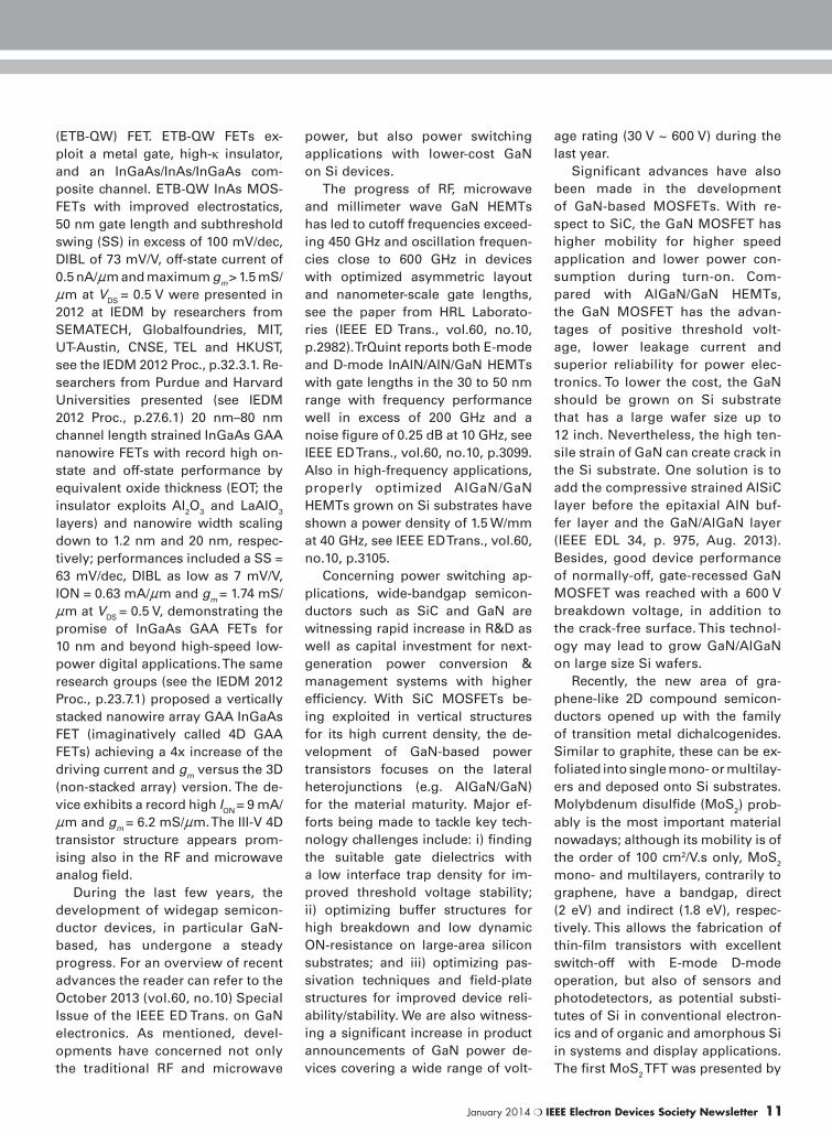
Research on compound semicon-
ductor (CS) electronics is showing
continuous advances in traditional
areas and new fields. Microwave and
mm-wave applications are
benefiting from further
developments in well-
established technolo-
gies (e.g. III-V HEMTs
and HBTs), while re-
search in III-V MOS-
FETs and FINFETs as
a possible alternative
to Si-based digital devices
has reached interesting milestones.
Progress in widegap (SiC and GaN)
electronics continues and a steady
improvement is seen in the related
reliability issues. Further
major advancements are
found for the applica-
tion of III-N concepts to
power electronics for
fast switching in ener-
gy conversion. At the
same time, the quest
for graphene-like 2D
semiconductors has also
found an interesting CS line in the 2D
transition metal chalcogenides.
The main driver of the develop-
ment of III-V MOSFETs lies in the
superior electron transport proper-
ties of III-V materials with respect
to Si, enabling an attractive route
to downscaling at sub 10 nm nodes.
Different architectures have been
considered for aggressively scaled
III-V devices; examples are the FIN-
FET, the Nanowire FET (also called
Gate All Around, GAA FET), the Ex-
tremely Thin Body Quantum Well
MESSAGE FROM THE EDS NEWSLETTER EDITOR-IN-CHIEF
EDS COMPOUND SEMICONDUCTOR DEVICES AND CIRCUITS TECHNICAL COMMITTEE REPORT
M.K. RadhakrishnanEditor-in Chief,
EDS Newsletter
January 2014 ❍ IEEE Electron Devices Society Newsletter 11
(ETB-QW) FET. ETB-QW FETs ex-
ploit a metal gate, high-κ insulator,
and an InGaAs/InAs/InGaAs com-
posite channel. ETB-QW InAs MOS-
FETs with improved electrostatics,
50 nm gate length and subthreshold
swing (SS) in excess of 100 mV/dec,
DIBL of 73 mV/V, off-state current of
0.5 nA/nm and maximum gm
> 1.5 mS/
nm at VDS
= 0.5 V were presented in
2012 at IEDM by researchers from
SEMATECH, Globalfoundries, MIT,
UT-Austin, CNSE, TEL and HKUST,
see the IEDM 2012 Proc., p.32.3.1. Re-
searchers from Purdue and Harvard
Universities presented (see IEDM
2012 Proc., p.27.6.1) 20 nm–80 nm
channel length strained InGaAs GAA
nanowire FETs with record high on-
state and off-state performance by
equivalent oxide thickness (EOT; the
insulator exploits Al2O
3 and LaAlO
3
layers) and nanowire width scaling
down to 1.2 nm and 20 nm, respec-
tively; performances included a SS =
63 mV/dec, DIBL as low as 7 mV/V,
ION = 0.63 mA/nm and gm
= 1.74 mS/
nm at VDS
= 0.5 V, demonstrating the
promise of InGaAs GAA FETs for
10 nm and beyond high-speed low-
power digital applications. The same
research groups (see the IEDM 2012
Proc., p.23.7.1) proposed a vertically
stacked nanowire array GAA InGaAs
FET (imaginatively called 4D GAA
FETs) achieving a 4x increase of the
driving current and gm versus the 3D
(non-stacked array) version. The de-
vice exhibits a record high ION
= 9 mA/
nm and gm
= 6.2 mS/nm. The III-V 4D
transistor structure appears prom-
ising also in the RF and microwave
analog field.
During the last few years, the
development of widegap semicon-
ductor devices, in particular GaN-
based, has undergone a steady
progress. For an overview of recent
advances the reader can refer to the
October 2013 (vol.60, no.10) Special
Issue of the IEEE ED Trans. on GaN
electronics. As mentioned, devel-
opments have concerned not only
the traditional RF and microwave
power, but also power switching
applications with lower-cost GaN
on Si devices.
The progress of RF, microwave
and millimeter wave GaN HEMTs
has led to cutoff frequencies exceed-
ing 450 GHz and oscillation frequen-
cies close to 600 GHz in devices
with optimized asymmetric layout
and nanometer-scale gate lengths,
see the paper from HRL Laborato-
ries (IEEE ED Trans., vol.60, no.10,
p.2982). TrQuint reports both E-mode
and D-mode InAlN/AlN/GaN HEMTs
with gate lengths in the 30 to 50 nm
range with frequency performance
well in excess of 200 GHz and a
noise figure of 0.25 dB at 10 GHz, see
IEEE ED Trans., vol.60, no.10, p.3099.
Also in high-frequency applications,
properly optimized AlGaN/GaN
HEMTs grown on Si substrates have
shown a power density of 1.5 W/mm
at 40 GHz, see IEEE ED Trans., vol.60,
no.10, p.3105.
Concerning power switching ap-
plications, wide-bandgap semicon-
ductors such as SiC and GaN are
witnessing rapid increase in R&D as
well as capital investment for next-
generation power conversion &
management systems with higher
efficiency. With SiC MOSFETs be-
ing exploited in vertical structures
for its high current density, the de-
velopment of GaN-based power
transistors focuses on the lateral
heterojunctions (e.g. AlGaN/GaN)
for the material maturity. Major ef-
forts being made to tackle key tech-
nology challenges include: i) finding
the suitable gate dielectrics with
a low interface trap density for im-
proved threshold voltage stability;
ii) optimizing buffer structures for
high breakdown and low dynamic
ON-resistance on large-area silicon
substrates; and iii) optimizing pas-
sivation techniques and field-plate
structures for improved device reli-
ability/stability. We are also witness-
ing a significant increase in product
announcements of GaN power de-
vices covering a wide range of volt-
age rating (30 V ~ 600 V) during the
last year.
Significant advances have also
been made in the development
of GaN-based MOSFETs. With re-
spect to SiC, the GaN MOSFET has
higher mobility for higher speed
application and lower power con-
sumption during turn-on. Com-
pared with AlGaN/GaN HEMTs,
the GaN MOSFET has the advan-
tages of positive threshold volt-
age, lower leakage current and
superior reliability for power elec-
tronics. To lower the cost, the GaN
should be grown on Si substrate
that has a large wafer size up to
12 inch. Nevertheless, the high ten-
sile strain of GaN can create crack in
the Si substrate. One solution is to
add the compressive strained AlSiC
layer before the epitaxial AlN buf-
fer layer and the GaN/AlGaN layer
(IEEE EDL 34, p. 975, Aug. 2013).
Besides, good device performance
of normally-off, gate-recessed GaN
MOSFET was reached with a 600 V
breakdown voltage, in addition to
the crack-free surface. This technol-
ogy may lead to grow GaN/AlGaN
on large size Si wafers.
Recently, the new area of gra-
phene-like 2D compound semicon-
ductors opened up with the family
of transition metal dichalcogenides.
Similar to graphite, these can be ex-
foliated into single mono- or multilay-
ers and deposed onto Si substrates.
Molybdenum disulfide (MoS2) prob-
ably is the most important material
nowadays; although its mobility is of
the order of 100 cm2/V.s only, MoS2
mono- and multilayers, contrarily to
graphene, have a bandgap, direct
(2 eV) and indirect (1.8 eV), respec-
tively. This allows the fabrication of
thin-film transistors with excellent
switch-off with E-mode D-mode
operation, but also of sensors and
photodetectors, as potential substi-
tutes of Si in conventional electron-
ics and of organic and amorphous Si
in systems and display applications.
The first MoS2 TFT was presented by
12 IEEE Electron Devices Society Newsletter ❍ January 2014
CALL FOR NOMINATIONS—IEEE FELLOW CLASS OF 2015
Kis et al. of EPFL in 2011 (see Nature
Nanotech., vol. 6, no. 3, pp. 147–150,
2011) but many research groups are
engaged in the development of this
technology, see e.g. the multilayer
MoS2 transistor presented at IEDM in
2012 (pp. 5.5.1–5.5.4) and the bilayer
MoS2 integrated circuits (implement-
ing logical functions and ring oscil-
lators) in Nano Letters, 2012, 12 (9),
pp. 4674–4680.
The 2013 EDS CSDC Committee
member list can be found at: http://
eds.ieee.org/technical-committees/
eds-compound-semiconductor-
devices-and-circuits-technical-
committee.html. Some of the CSDC
committee members have been
guest editors of the October 2013 ED
Trans. SI on GaN electron devices
and in the chapter RF and micro-
wave semiconductor technologies
of the EDS anniversary book Guide
to state-of-the-art electron devices,
J. Burghartz, ed., Wiley-IEEE, 2013.
Among future activities the EDS
CSDC Committee would continue
proposing special issues in the EDS
periodicals focused on recent devel-
opments in the area.
Giovanni Ghione
EDS CSDC
Technical Committee Chair
Politecnico di Torino, Italy
Kevin Chen
Hong Kong University of Science &
Technology
Albert Chin
National Chiao Tung University, Taiwan
Ruediger Quay
Fraunhofer Institute, Freiburg,
Germany
IEEE Fellow is a distinction reserved
for select IEEE members. The honor
is conferred by the Board of Direc-
tors upon a person with an extraor-
dinary record of accomplishments in
any of the IEEE fields of interest.
If you know of an IEEE colleague
who is a Senior Member or Life Se-
nior Member in good standing, has
completed five years of service in
any grade of IEEE Membership and
who has made an outstanding con-
tribution to the electronic or electrical
engineering profession in any of the
IEEE fields of interest, you can nomi-
nate this person in one of four cate-
gories: Application Engineer/Practi-
tioner, Educator, Research Engineer/
Scientist or Technical Leader. Nomi-
nations for the Fellow Class of 2015
are now being accepted.
To learn more about the Fel-
low program and the application
process, visit the Fellow Web Site
at http://www.ieee.org/fellows. The
deadline for nominations is March
1, 2014.
If you have been in professional practice for 10 years,
you may be eligible for Senior Membership, the highest
grade of membership for which an individual can apply.
New senior members receive a wood and bronze plaque
and a credit certificate for up to US $25 for a new IEEE
society membership. Upon request a letter will be sent
to employers, recognizing this new status.
Please remember to designate the Electron De-
vices Society as your nominating entity!
For more information on senior member status, visit:
http://www.ieee.org/membership_services/membership/
senior/index.html
To apply for senior member status, fill out the on-line
application: https://www.ieee.org/ membership_services/
membership/senior/application/index.html
You will need to Sign-in with your IEEE account.
CONGRATULATIONS TO THE 21 EDS MEMBERS RECENTLY ELECTED TO IEEE SENIOR MEMBER GRADE!
Khaled Addoweesh
Kerem Akarvardar
Mohammad Bukhari
Edward Cartier
John Cetnar
YoungHo Cho
* Individual designated EDS as nominating entity.
Robert Gateru
Bahram Ghodsian
Sanjay Ghosh
Zachary Griffith
Emanuel Istrate
Karol Kalna
Martin Kerber
Chien-Chung Lin
James Masi
Tapas Pal
Pierpaolo Palestri
Thomas Szkopek
Miguel Urteaga
Michael Wright
Gregary Zweigle

January 2014 ❍ IEEE Electron Devices Society Newsletter 13
ANNOUNCEMENT OF THE 2013 EDS PH.D. STUDENT FELLOWSHIP WINNERS
The Electron De-
vices Society Ph.D.
Student Fellow-
ship Program was
designed to pro-
mote, recognize,
and support Ph.D.
level study and re-
search within the
Electron Devices
Society’s field of in-
terest: The field of interest for EDS is all
aspects of engineering, physics, theory,
experiment and simulation of electron
and ion devices involving insulators,
metals, organic materials, plasmas,
semiconductors, quantum-effect mate-
rials, vacuum, and emerging materials.
Specific applications of these devices in-
clude bioelectronics, biomedical, com-
putation, communications, displays,
electro and micro mechanics, imaging,
micro actuators, optical, photovoltaics,
power, sensors and signal processing.
The Society is concerned with
research, development, design and
manufacture related to materials,
processing, technology, and appli-
cations of such devices, and scien-
tific, technical, educational and other
activities that contribute to the ad-
vancement of this field.
EDS proudly announces three
EDS Ph.D. Student Fellowship win-
ners for 2013. Brief biographies of
the recipients appear below. De-
tailed articles about each Ph.D. Stu-
dent Fellowship winner and their
work will appear in forthcoming is-
sues of the EDS Newsletter.
Tarek Zaki (S’07)
received the B.Sc.
degree (with high -
est honors) in
in formation en-
gineering and
technology from
the German Uni-
versity in Cairo (GUC), Egypt, in 2009,
and the M.Sc. degree (with distinc-
tion) in micro- and optoelectronics
from the University of Stuttgart, Ger-
many, in 2010. He joined the Institute
for Microelectronics Stuttgart (IMS
CHIPS) and the Institute for Nano-
and Microelectronic Systems (INES),
Germany, as a researcher in 2010 and
2011, respectively, where he is cur-
rently working towards the Ph.D. de-
gree under the supervision of Prof.
Dr.-Ing. Joachim N. Burghartz. His re-
search focuses on the development of
world’s fastest low-voltage thin-film
transistors and mixed-signal circuits
based on organic semiconductors.
He authored/co-authored more than
15 peer-reviewed, papers at top publi-
cation venues. He is a member of the
IEEE EDS and SSCS.
Hong-Yu (Henry)
Chen received
his B.S. degree
from National Ts-
ing Hua University
(NTHU), Hsinchu,
Taiwan, in 2007
and his M.S. de-
gree from Stan-
ford University, CA, in 2011, both in
electrical engineering. He is currently
pursuing his Ph.D. degree at Stanford
University under the supervision of
Prof. H.-S. Philip Wong.
Henry’s research interests at
Stanford include (1) processing
technology and the characterization
of emerging resistive switching
memory; (2) carbon nanotubes ma-
terial synthesis, device character-
ization, and circuit integration. To
date, he has authored/coauthored
40+ technical papers, including 1
ISSCC, 4 VLSI, and 7 IEDM papers.
His papers have been cited more
than 150 times since 2010 with
H-index 7.
Henry held summer internship
positions at Applied Materials Inc.,
IMEC, and SanDisk Inc. in 2011,
2012, and 2013 respectively. He
is the recipient of several awards,
including the Intel Fellowship 2013–
2014, Taiwanese Government schol-
arships to study abroad (GSSA)
2012–2014, the IEEE Electron De-
vices Society Ph.D. Student Fel-
lowship 2013, and the Best Student
Paper Award of the 2011 VLSI Tech-
nology Symposium.
He Tian received
the B.S. degrees
from HeFei Uni-
versity of Tech-
nology, China in
2010. Since 2010,
he has worked
at the Institute
of Microelectron-
ics, Tsinghua University, China, as
a Ph.D. student. He is currently a
young team leader investigating
novel flexible graphene-based de-
vices. He has already published 12
first-authored papers, which ap-
peared in top venues such as Nano
Letters, ACS Nano, Scientific Re-
ports, Nanoscale, Applied Physics
Letters, etc. He has also reported
his research outcomes at top con-
ferences such as the IEEE IEDM and
MEMS. Mr. Tian has been an active
student volunteer for EDS activities
and serves as Vice Chair of the IEEE
EDS Tsinghua University Student
Chapter.
Agis Iliadis
EDS Student Fellowship Chair
University of Maryland
College Park, MD, USA
Agis IliadisEDS Student
Fellowship Chair
14 IEEE Electron Devices Society Newsletter ❍ January 2014

January 2014 ❍ IEEE Electron Devices Society Newsletter 15
ANNOUNCEMENT OF THE 2013 EDS MASTERS STUDENT FELLOWSHIP WINNERS
The Electron Devic-
es Society Masters
Student Fellow-
ship Program was
designed to pro-
mote, recognize,
and support Mas-
ters level study and
research within the
Electron Devices
Society’s field of
interest. The field of interest for EDS
is all aspects of engineering, physics,
theory, experiment and simulation
of electron and ion devices involving
insulators, metals, organic materials,
plasmas, semiconductors, quantum-
effect materials, vacuum, and emerg-
ing materials. Specific applications of
these devices include bioelectronics,
biomedical, computation, communi-
cations, displays, electro and micro
mechanics, imaging, micro actuators,
optical, photovoltaics, power, sensors
and signal processing.
The Society is concerned with
research, development, design and
manufacture related to materials,
processing, technology, and appli-
cations of such devices, and scien-
tific, technical, educational and other
activities that contribute to the ad-
vancement of this field.
EDS proudly announces three
winners of the 2013 EDS Masters
Student Fellowship. Brief biogra-
phies of the recipients appear below.
Detailed articles about each Masters
Student Fellowship winner and their
work will appear in forthcoming is-
sues of the EDS Newsletter.
Enes Battal re-
ceived the B.S.
degree in Electri-
cal and Electron-
ics Engineering
from Bilkent Uni-
versity, Ankara,
Turkey. He is cur-
rently pursuing his Master’s Degree
under supervision of Asst. Prof. Ali
Kemal Okyay in the same depart-
ment. His undergraduate research
activities focused on utilizing sur-
face plasmons to achieve functional
structures and enhanced optical ab-
sorption. He is currently working on
development and characterization
of actively tunable optical materi-
als and their use in the realization of
novel reconfigurable optical nanode-
vices. He is also interested in devel-
opment of material a lternatives to
metals to be used in plasmonics. He
has authored or co-authored 5 jour-
nal papers and more than 10 confer-
ence papers.
Zhongyu Li is a
graduate student
at the University
of Electronic Sci-
ence and Technol-
ogy of China. His
research interests
mainly concern
novel radar imaging. Till now, he has
published five papers on several in-
ternational journals and conferences,
and also published six papers as the
second author in IEEE Transactions
on Geoscience and Remote Sensing,
IEEE Transactions on Aerospace and
Electronic Systems, etc. He has suc-
cessfully applied six Chinese patents
for invention.
During his undergraduate study,
Zhongyu was awarded with the Na-
tional Scholarship in 2009 and 2010.
In June 2012, he was awarded Excel-
lent Undergraduate Student of Sich-
uan province.
Yang Lu received
the B.S degree in
Microelectronics
from Peking Uni-
versity, Beijing,
China, in 2012. He
is currently work-
ing toward the
M.S. degree at the University of Penn-
sylvania, Philadelphia, Pennsylvania.
Since 2011, Yang Lu has been working
on Resistive Random Access Memory
(RRAM) in various material systems,
including metal oxide based, filamen-
tary RRAM and silicon based, nano-
metallic RRAM. He and his colleagues
investigated switching mechanisms
and degradation behaviors in RRAM
and developed a simplified model
for RESET process. He has published
his work in IEEE Electron Device Let-
ters, IEDM 2011, IRPS 2012, NVMTS
2013, etc.
Agis Iliadis
EDS Student
Fellowship Chair
University of Maryland
College Park, MD, USA
Agis IliadisEDS Student
Fellowship Chair

16 IEEE Electron Devices Society Newsletter ❍ January 2014
PROJECT ELECTRON JOINS LOCAL SCIENCE FAIR
In 2012, Project Electron joined the
Science Circuit of Planaltina, becom-
ing a partner in initiatives promoted
by the Secretary of Education of the
Federal District of Brazil.
The project was presented to
an audience composed mainly of
students from primary and second-
ary public schools. Tests were per-
formed using donated Elenco Snap
Circuits® kits that included FM radio
and human transistor experiments.
Several teachers expressed inter-
est in the project and requested infor-
mation for possible implementation
in their schools. It was very enriching
to attend this event because it was
an opportunity to demonstrate this
program to more communities and
educators.
Rafael Amral Shayani
IEEE Centro-Norte Brasil
Section Chair

January 2014 ❍ IEEE Electron Devices Society Newsletter 17

18 IEEE Electron Devices Society Newsletter ❍ January 2014
The EDS Distinguished Lecturer (DL)
Program exists for the purpose of
providing EDS Chapters with a list of
quality lecturers who can potentially
give talks at local chapter meetings.
To arrange for a lecture, EDS chap-
ters should visit the EDS website to
view the listing of EDS DLs and contact
the EDS DL directly. A general guide-
line for the visit, but not the absolute
rule, is that the lecturer should be
able to include the meeting site with
an already planned travel schedule at
a small incremental cost to the travel
plan. Although the concept of the pro-
gram is to have the lecturers minimize
travel costs by combining their visits
with planned business trips, EDS will
help subsidize lecturer travel in cases
where few/no lecturers will be visiting
an area and/or a chapter cannot pay
for all the expenses for a lecturer trip.
EDS is also encouraging Distin-
guished Lecturer clusters/mini-collo-
quia (MQ) to remote areas. This con-
cept generally involves the sending
of about 2 or more DLs to travel to a
region/chapter and present the latest
developments in a particular field. The
chapters/regions would be responsi-
ble for handling all the arrangements
of the event and only minimal finan-
cial support would be required of EDS
and could be covered by the MQ Pro-
gram budget upon request.
For more information on the DL
or MQ Programs, please visit the
EDS website or contact Laura Riello
of the EDS Executive Office.
Interested in know-
ing why it’s not pos-
sible to measure
the built-in voltage
of a PN junction us-
ing a voltmeter? Do
you need to under-
stand the best way
to derive an expres-
sion for the average
thermal velocity of
an electron? Or are you curious about
what quantum dots and wires are? The
answers to these questions and more are
available through the QuestEDS Ques-
tion and Answer page.
To ask a question not already
addressed on the Q&A page, visit
www.ieee.org/go/questeds. Techni-
cal experts answering the questions
posed represent academic, govern-
ment, and industry sectors.
Questions are grouped into nine
technical categories and two general
ones. Technical categories cover sub-
ject areas like semiconductor and de-
vice physics, process technology, de-
vice characterization, technology CAD,
compact modeling, VLSI interconnects,
photovoltaics, and quantum electron-
ics. Subject areas addressed are an-
ticipated to expand in the future. Two
other categories address questions
pertaining to educational activities and
general inquiries about society mem-
bership. Within a two week time frame
from when the question is asked, an
answer is posted online. Incoming
questions are handled by an editor-in-
chief who ensures that they fall within
the technical scope of EDS and that
they are adequately answered.
For the answer to this recent
submission, visit http://eds.ieee.org/
member-sign-in-form.html?notauth=1.
Your IEEE login is required to view the
answer page. After authentication you
will be redirected to the answer page,
where you can select the appropriate
topic link.
Samar Saha
EDS Vice-President of Publications
Ultrasolar Technology
Santa Clara, CA, USA
EDS DISTINGUISHED LECTURER AND MINI-COLLOQUIA PROGRAMS
QUESTEDS
Samar SahaEDS Vice-President
of Publications
Organic Semiconductor Devices
Question 060–13
Considering that an organic semiconductor, such as “Tips-pentacene”, was
spin-coated on top of an aluminum sheet, sintered and subjected to a final
3rd layer of gold (applied using a square shadow mask), what would be an
appropriate set of formulas that would predict the current dynamics as a
function of the voltage and geometry of the layers in this Schottky device?
If the same experiment were performed, but this time applying the tips-
pentacene by drop-cast, how should expectedly vary the results? Does the
rugosity of the layers affect the performance of the device? Why should
one consider the rugosity relevant?
Photovoltaics
Question 061–13
In a solar cell, we want to collect the photo-generated electrons and
holes in separate terminals and so we want them not to recombine
before collection. In a multi-junction solar cell, current flows from
one pn junction to another through tunnel junction, where electron makes
a tunneling jump from conduction band to valence band and with so many
holes in the valance band, the jumping electron should recombine with
hole. So, how can the photo-generated electrons and holes make it to the
opposite electrode without recombination in a multi-junction solar cell?

January 2014 ❍ IEEE Electron Devices Society Newsletter 19
2011–2012 EDS REGION 9 OUTSTANDING STUDENT PAPER AWARD
The Electron Devices Society confers
its prestigious Region 9 Outstand-
ing Student Paper Award to the best
Region 9 student paper published in
an internationally recognized IEEE
sponsored journal or conference in
the field of electron devices related
topics. The winning paper is entitled,
“Surface-Potential-Based Drain Cur-
rent Analytical Model for Triple-Gate
Junctionless Nanowire Transistors.”
This paper was published in the IEEE
Transactions on Electron Devices, and
was authored by Renan Trevisoli Doria,
Rodrigo Trevisoli Doria, Michelly de
Souza, Samaresh Das, Isabelle Fer-
ain, and Marcelo Antonio Pavanello.
The award was presented at SBMi-
cro 2013, which was held Septem-
ber 3–6, 2013, in Curitiba, Brazil. The
Award consists of a certificate and
reimbursement of up to US $1,500 to
cover one author’s travel and accom-
modations to attend the conference.
On behalf of the Electron Devices Soci-
ety, I would like to congratulate Renan
Trevisoli Doria and the remaining au-
thors for this achievement. Brief biog-
raphies of all the authors of the paper
are given below.
Renan Trevisoli
Doria received
the electrical En-
gineering degree
from Centro Uni-
versitário da FEI,
Brazil, in 2007, re-
ceiving the awards
“Prêmio CREA-SP de Formação
Profissional” and “Instituto de En-
genharia” given for the best student
among the 7 modalities of engineer-
ing courses offered at FEI. In 2010 he
received the M. Sc. degree in Micro-
electronics from Centro Universitário
da FEI and in April 2013 he received
the Ph.D. degree in Microelectronics
from University of São Paulo, Brazil.
In February 2012, he was with Tyndall
National Institute, Cork, Ireland, for
electrical characterization of Junction-
less Nanowire Transistors. His current
interests are electrical characteriza-
tion, modeling and simulation of SOI
multiple gate devices.
Rodrigo Trevisoli
Doria received
the Electrical En-
gineering degree
and the M. Sc. de-
gree in integrated
electronic devices
from Centro Uni-
versitário da FEI in 2003 and 2007,
respectively, and the Ph.D. degree
in microelectronics from University
of São Paulo, São Paulo, Brazil, in
2010. From November 2009 to March
2010 he was with Tyndall National
Institute, University College Cork,
Ireland, working with the simula-
tion and electrical characterization of
Junctionless Nanowire Transistors
(JNTs). He is currently a Postdoc Re-
searcher with Centro Universitário
da FEI. He is Member of the Brazilian
Microelectronics Society and his cur-
rent research interests are focused
on the simulation, electrical char-
acterization, and modeling of SOI
CMOS transistors.
Michelly de Souza
(S’05–M’08) receiv -
ed the Electrical
Engineering de-
gree from Centro
Universitário da
FEI in 2002, and
the M. Sc. and
Ph.D. degrees in 2005 and 2008,
respectively, in Microelectronics
from University of São Paulo, Bra-
zil. From September 2007 to Febru-
ary 2008 she was with Laboratoire
de Microélectronique from Univer-
sité Catholique de Louvain, Bel-
gium, working in the fabrication and
electrical characterization of analog
circuits with Silicon-On-Insulator
transistors. She is currently Associ-
ate Professor at Centro Universitário
da FEI, Brazil. She is Member of both
the IEEE Electron Devices Society
and the IEEE Solid State Circuits and
Systems Society, and the Brazilian
Microelectronics Society. Her current
interests are the electrical character-
ization, simulation and modeling of
SOI devices.
Samaresh Das
received the M.
Sc. and Ph.D. de-
gree in physics
from Indian Insti-
tute of Technol-
ogy Kharagpur,
India, in 2005
and 2011, respectively. At Indian In-
stitute of Technology, his research
involved on Ge quantum dot based
floating gates, light emitters and
photo-detectors on silicon substrate.
He then worked as a researcher in
the Ultimate Silicon Device Group
led by Jean-Pierre Colinge at Tyn-
dall National Institute, Ireland. There
he worked on the fabrication and
characterization of Junctionless
Nanowire Field Effect Transistors. In
November 2012, he joined the Hi-
tachi Cambridge Laboratory, Caven-
dish Laboratory. He currently works
on silicon based quantum informa-
tion technology.
Isabelle Ferain
received the M.Sc.
Degree in Applied
Sciences from
the University of
Mons, Mons, Bel-
gium and the M.
Sc. Degree in Elec-
trical Engineering from the Ecole Su-
perieure d’Electricite, Orsay, France,
in 2001. She received the Ph.D.

20 IEEE Electron Devices Society Newsletter ❍ January 2014
Degree in Electrical Engineering from
the Katholieke Universiteit Leuven,
Leuven, Belgium, in 2008. She has au-
thored or co-authored more than 100
peer-reviewed publications and con-
ference contributions on nano-tech-
nologies, and has co-authored 4 book
chapters on SOI and nanowire field
effect transistors. She has been with
ON Semiconductor, Oudenaarde, Bel-
gium, with IMEC, Leuven, Belgium,
and with Tyndall National Institute,
Cork, Ireland where she worked on
the fabrication and characterization
of SOI Multiple-gate FETs. She is cur-
rently a member of the technical staff
in Globalfoundries, Malta, New York,
working in the Technology Develop-
ment group.
Marcelo Antonio
Pavanello (S’99–
M ’ 0 2 – S M ’ 0 5 )
received the Elec-
trical Engineering
degree from Cen-
tro Universitário
da FEI in 1993,
and the M.Sc. and Ph.D. degrees in
Microelectronics from University of
São Paulo, São Paulo, Brazil, in 1996
and 2000, respectively. In 2003, he
became Professor at Electrical En-
gineering Department of FEI. From
November 2008 to February 2009,
he was with the Laboratoire de Mi-
croélectronique, Université Catholique
de Louvain, Louvain-la-Neuve, Bel-
gium, as Visiting Professor. He has
authored or coauthored more than
170 technical papers in journals and
conferences, and was an author/edi-
tor of six books. Dr. Pavanello is an
IEEE EDS Distinguished Lecturer.
Jacobus Swart
EDS Region 9 Outstanding
Student Paper Award Chair
State University of Campinas
Brazil
2013 EDS CHAPTER OF THE YEAR AWARD
The EDS Chapter of the Year Award is presented annually
to recognize EDS chapters for the quality and quantity
of the activities and programs implemented during the
prior July–June period.
The EDS BoG recently approved a change in the EDS
Chapter of the Year Award to recognize more Chapters
region wise. Four awards are being decided for this year,
one each for Region 1-7, Region 8, Region 9 and Region
10. The selection criterion remains the same as previous
years.
The 2013 EDS Chapter of the Year Award winners are:
Regions 1–7: ED/SSC Baltimore Chapter
Region 8: ED IRE NASU Kharkiv Student Branch Chapter
Region 9: ED/MTT/EMB Brazil Chapter
Region 10: ED Delhi Chapter
Xing Zhou
EDS Vice-President of Regions/Chapters
Nanyang Technological University
Singapore
Illia Fedorin—Region 8 ED IRE NASU Kharkiv Student Branch Chapter Chair
Naresh Das—Regions 1-7 ED SSC Baltimore Chapter Chair
Fabiano Araujo Soares—Region 9 ED MTT EMB Brazil Chapter Chair
Mridula Gupta—Region 10 ED Delhi Chapter Chair

January 2014 ❍ IEEE Electron Devices Society Newsletter 21
R E G I O N A L A N D C H A P T E R N E W S
ED Santa Clara Valley–by Toshishige Yamada
On September 6, 2013, the ED Santa
Clara Valley Chapter held its annual
Power Electronics Symposium. This
year’s event titled, “Beyond the
Silicon Limit,” was located at the TI
Auditorium, in Santa Clara, Califor-
nia. The symposium attracted 106
attendees, 76 of whom were IEEE
members.
Power electronics is re-emerging
as an important and innovative area.
This is due to the increasing impor-
tance of electricity in our lives, and
the need to use it more efficiently.
The old paradigm involved large in-
ductors and capacitors, slow silicon
devices, and a barrier known as the
“silicon limit.” The new revolution is
fueled not only by improved Si device
technology using conductivity and
field-modulation, but also by excit-
ing new materials GaN and SiC that
have taken devices beyond the sili-
con limit. Designers are making use
of this substantially improved per-
formance to increase efficiency and
reduce size. The half-day symposium
had presentations from leading con-
tributors in the multidisciplinary field
of power electronics. Topics included
Si, SiC and GaN device technology,
the bottlenecks to power switching,
and power electronics applications.
The symposium was of significant
interest to both device and circuit
engineers, students and experts,
who wished to develop a broader
perspective and increase their depth
and breadth of knowledge.
Attendees were privileged to hear
the following speakers:
• Deva Pattanayak (Senior Director
at Vishay Siliconix)—“High
Voltage Silicon Power Devices
below the Silicon Limit”
• Alex Lidow (CEO of EPC)—“GaN
—the End of the Road for Si”
• Dave Anderson (Chief Technol-
ogist and General Manager of
Texas Instruments Kilby Labs Sil-
icon Valley)—“Power Electronics
Applications”
• Johan Strydom (Head of
Applications Engineering at
EPC)—“Barriers to High-speed
Switching in Power Devices”
• Don Disney (Sr. Director of
Technology and Product Develop-
ment at Avogy)—“Vertical Power
Devices in Bulk GaN Substrates”
~ Adam Conway, Editor
USA, CANADA & LATIN AMERICA (REGIONS 1–6,
7 & 9)
Sandeep Bahl, EDS Chapter Vice-Chair (left) and Don Disney, Avogy (right)
Toshishige Yamada, EDS SCV Chapter Chair
Presentation by Dave Anderson, Texas Instruments
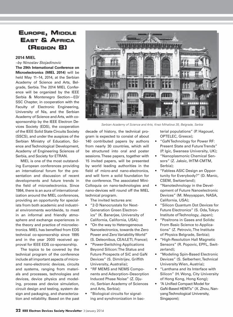
22 IEEE Electron Devices Society Newsletter ❍ January 2014
2014 MIEL–by Ninoslav Stojadinovic
The 29th International Conference on Microelectronics (MIEL 2014) will be
held May 11–14, 2014, at the Serbian
Academy of Science and Arts, Bel-
grade, Serbia. The 2014 MIEL Confer-
ence will be organized by the IEEE
Serbia & Montenegro Section—ED/
SSC Chapter, in cooperation with the
Faculty of Electronic Engineering,
University of Nis, and the Serbian
Academy of Science and Arts, with co-
sponsorship by the IEEE Electron De-
vices Society (EDS), the cooperation
of the IEEE Solid State Circuits Society
(SSCS), and under the auspices of the
Serbian Ministry of Education, Sci-
ence and Technological Development,
Academy of Engineering Sciences of
Serbia, and Society for ETRAN.
MIEL is one of the most outstand-
ing European conferences providing
an international forum for the pre-
sentation and discussion of recent
developments and future trends in
the field of microelectronics. Since
1984, there is an aura of international-
ization around the MIEL conferences,
providing an opportunity for special-
ists from both academic and industri-
al environments worldwide, to meet
in an informal and friendly atmo-
sphere and exchange experiences in
the theory and practice of microelec-
tronics. MIEL has benefited from EDS
technical co-sponsorship since 1995
and in the year 2000 received ap-
proval for IEEE EDS co-sponsorship.
The topics to be covered by the
technical program of the conference
include all important aspects of micro-
and nano-electronic devices, circuits
and systems, ranging from materi-
als and processes, technologies and
devices, device physics and model-
ing, process and device simulation,
circuit design and testing, system de-
sign and packaging, and characteriza-
tion and reliability. Based on the past
decade of history, the technical pro-
gram is expected to consist of about
140 contributed papers by authors
from nearly 30 countries, which will
be structured into oral and poster
sessions. These papers, together with
15 invited papers, will be presented
by world leading authorities in the
field of micro-and nano-electronics,
and will form a solid foundation for
the conference. The associated Mini-
Colloquia on nano-technologies and
nano-devices will round off the MIEL
technical program.
The invited lectures are:
• “2-D Nanocrystals for Next-
Generation Green Electron-
ics” (K. Banerjee, University of
California, California, USA);
• “On the way to Heterogeneous
Nanoelectronics, towards the Zero
Power and Zero Variability World”
(S. Deleonibus, CEA/LETI, France);
• “Power-Switching Applications
Beyond Silicon: The Status and
Future Prospects of SiC and GaN
Devices” (S. Dimitrijev, Griffith
University, Australia);
• “RF MEMS and NEMS Compo-
nents and Adsorption–Desorption
Induced Phase Noise” (Z. Dju-
ric, Serbian Academy of Sciences
and Arts, Serbia);
• “Biological circuits for signal-
ing and synchronization in bac-
terial populations” (P. Hagouel,
OPTELEC, Greece);
• “GaN Technology for Power RF:
Present State and Future Trends”
(P. Igic, Swansea University, UK);
• “Nanoplasmonic Chemical Sen-
sors” (Z. Jaksic, IHTM-CMTM,
Serbia);
• “Fabless ASIC Design an Oppor-
tunity for Everybody?” (D. Manic,
CSEM, Switzerland);
• “Nanotechnology in the Devel-
opment of Future Nanoelectronic
Devices” (M. Meyyappan, NASA,
California, USA);
• “Silicon Quantum Dot Devices for
Future Electronics” (S. Oda, Tokyo
Institute of Technology, Japan);
• “Positrons in Gases and Solids:
From Basic Science to Applica-
tions” (Z. Petrovic, The Institute
of Physics Belgrade, Serbia);
• “High-Resolution Hall Magnetic
Sensors” (R. Popovic, EPFL, Swit-
zerland);
• “Modeling Spin-Based Electronic
Devices” (S. Selberherr, Technical
University Wien, Austria);
• “Lanthana and its Interface with
Silicon” (H. Wong, City University
of Hong Kong, Hong Kong);
• “A Unified Compact Model for
GaN-Based HEMTs” (X. Zhou, Nan-
yang Technological University,
Singapore);
Serbian Academy of Science and Arts, Knez Mihailova 35, Belgrade, Serbia
EUROPE, MIDDLE EAST & AFRICA
(REGION 8)

January 2014 ❍ IEEE Electron Devices Society Newsletter 23
Belgrade is the capital and largest
city of Serbia and has a population of
about 1.6 million. It is situated in south-
eastern Europe, on the Balkan Pen-
insula, at the confluence of the Sava
and Danube Rivers where the Panno-
nian Plain meets the Balkans. It is one
of the oldest cities in Europe and has
since ancient times been an important
focal point for traffic, an intersection
of the roads of Eastern and Western
Europe. Belgrade is the capital of Ser-
bian culture, education, science and
economy. As a result of its tumultu-
ous history, Belgrade has for centu-
ries been home to many nationalities,
with Serbs of the Orthodox Christian
religion making up the majority of the
population (90%). Belgrade is the seat
of the highest scientific and research
institutions in all fields. Serbian Acad-
emy of Sciences and Arts, one of the
organizers of the MIEL 2014 Confer-
ence, founded in 1886 as the Serbian
Royal Academy, is a leader of the Ser-
bian scientific society in many scien-
tific and artistic areas.
For registration and other informa-
tion, visit the 2014 MIEL Home Page
at http://miel.elfak.ni.ac.rs, or contact
the MIEL Conference Secretariat, De-
partment of Microelectronics, Faculty
of Electronic Engineering, University
of Nis, A. Medvedeva 14, 18000 Nis,
Serbia; Telephone: +381 18 529 326;
Fax: +381 18 588 399; E-mail: miel@
elfak.ni.ac.rs.
The MIEL organizers and commit-
tee members look forward to seeing
you in May 2014.
2013 MIXDES–by Mariusz Orlikowski
On June 20–22, 2013, in Gdynia,
Poland, the annual 20th Interna-
tional Conference “Mixed Design
of Integrated Circuits and Systems”
—MIXDES, was held. The event
was organized by the Technical Uni-
versity of Lodz, the Warsaw Uni-
versity of Technology and Gdynia
Maritime University. The conference
was co-sponsored by The Institute
of Electrical and Electronics Engi-
neers, Poland Section IEEE Election
Devices and the Circuits and Systems
Societies, and the Polish Academy
of Sciences, Committee of Electron-
ics and Telecommunication, Section
of Microelectronics and Section of
Signals and Electronic Circuits and
Systems. The conference was at-
tended by more than 120 scientists
from around the world, representing
21 countries.
The comprehensive conference
program of 115 presentations consist-
ed of oral, poster and special sessions.
This year, the MIXDES 2013 organiz-
ing committee had the pleasure to in-
vite six keynote speakers:
• V. Axelrad (SEQUOIA Design Sys-
tems, Inc., USA), Design and
Simulation of ESD-Resistant ICs
• Y.S. Chauhan (Indian Institute
of Technology, Kanpur, INDIA),
BSIM Compact MOSFET Models
for SPICE Simulation
• X. Zhou (Nanyang Technolog-
ical University, SINGAPORE),
Top-down Drift-diffusion versus
Bottom-up Quasi-ballistic Formal-
ism in Device Compact Modeling
• G. Wachutka (Munich University
of Technology, GERMANY), The
Art of Modeling and Predictive
Simulation in Power Electronics
and Microsystems
• M.H. Fino (University Nova de
Lisboa, PORTUGAL), On the Use
of Compact Modeling for RF/
Analog Design Automation
• H. Toshiyoshi (University of Tokyo,
JAPAN), A Mixed-Design Tech-
nique for Integrated MEMS Using
a Circuit Simulator with HDL
In addition to the regular program,
two special sessions were held:
• Compact Modeling for More than
Moore, organized by Dr. Daniel
Tomaszewski (Institute of Elec-
tronic Technology, Poland) and
Dr. Władysław Grabinski (GMC
Suisse)
• xTCA for Instrumentation, or-
ganized by Dariusz Makowski,
Adam Piotrowski (Lodz Universi-
ty of Technology, Poland), Holger
Schlarb (DESY, Germany) and
Stefan Simrock (ITER, France)
Based on evaluations of the qual-
ity of the papers and presentations,
ten of the papers received the Best
Paper Award. Additionally Christian
Kauth, Marc Pastre and Maher Kayal
from EPFL, Switzerland received the
IEEE Poland Section ED Society Spe-
cial Award, presented by the Chapter
Chairman.
The 2014 MIXDES Conference
will take place in Lviv, Ukraine, as a
partner of the 6th International Con-
ference Microwave and Radar Week
(MRW-2014). The Preliminary Call for
Papers is available at http://www.
mixdes.org/downloads/mrw2014.
pdf. More information on past and
future MIXDES Conferences can be
found at http://www.mixdes.org.
Participants of the MIXDES Conference, Gdynia, Poland

24 IEEE Electron Devices Society Newsletter ❍ January 2014
ED Poland–by Henryk M. Przewłocki
An IEEE EDS Distinguished Lecture
(DL) was organized on June 21, 2013,
at the Institute of Electron Technology
(IET) in Warsaw, Poland. Prof. Hiroshi
Iwai of the Tokyo Institute of Technol-
ogy (TIT), and EDS Distinguished
Lecturer, presented a talk titled, “Fu-
ture of Nano CMOS Technology.” The
audience of this event, of approxi-
mately 40 people, was composed of
IET staff and guests from other Polish
institutes and abroad.
Since the group of TIT researchers
lead by Prof. Iwai is at the forefront
of new developments in nano CMOS
technologies, the lecture was a very
competent and clear presentation of
the DL’s opinions on further develop-
ments in this area during the coming
10-15 years. The audience enjoyed
very much the clear and well-moti-
vated opinions of Dr. Iwai.
~ Zygmunt Ciota, Editor
ED/PHO Dublin–by Patrick McNally
The Joint chapter of the Dublin
Electron Devices and the Ireland
Photonics Societies hosted the Pres-
ident-Elect of the Electron Devices
Society and Distinguished Lecturer,
Professor Albert Wang, on October 3,
2013, at Dublin City University. Pro-
fessor Wang, of the University of Cali-
fornia, Riverside, delivered a seminar
entitled “Concurrent Design of RF
Integrated Circuits (ICs) and Electro-
static Discharge (ESD) Protection.”
On-chip ESD protection design is a
grand challenge in RF IC manufacture
and Professor Wang’s talk discussed
critical aspects in practical designs,
including a mixed-mode ESD sim-
ulation-design method for RF ESD
protection design optimization and
prediction, accurate RF ESD design
characterization, complex ESD-IC in-
teractions, and ESD+RFIC co-design
techniques for whole-chip design op-
timization.
The talk was attended by more
than 30 academic staff and students,
as well as other local IEEE members.
Using the facilities of Ireland’s Nation-
al Nanotechnology Platform, INSPIRE,
the lecture was video-linked live to the
Tyndall National Institute in Cork and
the University of Limerick. After the
seminar, there was also an opportu-
nity to network and meet the speaker.
ED Scotland–by Jonathan Terry
In its efforts to increase its profile in
the technical community, the Scot-
tish chapter of EDS was a technical
co-sponsor of the IEEE International
Conference on Simulation of Semi-
conductor Processes and Devices
(SISPAD 2013), which was held in
Glasgow last September. The chap-
ter provided the IEEE ED Scotland
Best Student Paper Award, which was
won by Juan Pablo Duarte of the Uni-
versity of California, Berkeley, for his
paper Unified FinFET Compact Mod-
el: Modelling Trapezoidal Triple-Gate
Prof. Hiroshi Iwai (5th from left), accompanied by some of the event attendees at the Institute of Electron Technology (IET) in Warsaw, Poland
Professor Albert Wang pictured at Dublin City University with some of the IEEE members who attended his presentation
Dr. Albert Wang at Dublin City University
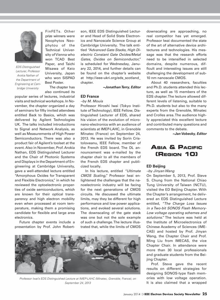
January 2014 ❍ IEEE Electron Devices Society Newsletter 25
FinFETs. Other
prize winners were
Neophytos Neo-
phytou of the
Technical Univer-
sity of Vienna who
won TCAD Best
Paper, and Taichi
Misawa of Keio
University, Japan
who won SISPAD
Best Poster.
The chapter has
also continued its
popular series of lectures, industrial
visits and technical workshops. In No-
vember, the chapter organized a day
of seminars for fifty invited attendees
entitled Back to Basics, which was
delivered by Agilent Technologies
UK. The talks included introductions
to Signal and Network Analysis, as
well as Measurements of High Power
Semiconductors. There was also a
product fair of Agilent’s toolset at the
event. Also in November, Prof. Arokia
Nathan, EDS Distinguished Lecturer
and the Chair of Photonic Systems
and Displays in the Department of En-
gineering at Cambridge University,
gave a well-attended lecture entitled
“Amorphous Oxides for Transparent
and Flexible Electronics,” in which he
reviewed the optoelectronic proper-
ties of oxide semiconductors, which
are known for their optical trans-
parency and high electron mobility
even when processed at room tem-
perature, making them a promising
candidate for flexible and large area
electronics.
Future chapter events include a
presentation by Prof. John Robert-
son, IEEE EDS Distinguished Lectur-
er and Head of Solid State Electron-
ics and Nanoscale Science Group at
Cambridge University. The talk enti-
tled “Advanced Gate Stacks, High Di-
electric Constant Gate Oxides/Metal
Gates, Oxides on Semiconductor,”
is scheduled for Wednesday, Janu-
ary 22, 2014, and further details can
be found on the chapter’s website
at http://ieee-ukri.org/eds_scotland_
chapter.
~Jonathan Terry, Editor
ED France–by M. Mouis
Professor Hiroshi Iwai (Tokyo Insti-
tute of Technology), IEEE Fellow, Dis-
tinguished Lecturer of EDS, shared
his vision of the evolution of micro-
nano-electronics with an audience of
scientists at IMEP-LAHC, in Grenoble
Minatec (France) on September 24,
2013. He was invited by Sorin Cris-
toloveanu, IEEE Fellow, member of
the French EDS board. The DL an-
nouncement was e-mailed by the
chapter chair to all the members of
the French EDS chapter and publi-
cized locally.
In his lecture, entitled “Ultimate
CMOS Scaling,” Professor Iwai en-
lightened the challenges that the na-
noelectronic industry will be facing
for the next generations of CMOS
circuits. He discussed the ultimate
limits, may they be different for high
performance and low power applica-
tions, and evoked several solutions.
The downscaling of the gate stack
was one but not the sole example
of such a challenge. The lecture illus-
trated that, while the limits of CMOS
downscaling are approaching, no
real competitor has yet emerged.
Professor Iwai documented the state
of the art of alternative device archi-
tectures and technologies. His mes-
sage was that the research efforts
need to be intensified in selected
domains, despite numerous, dif-
ficult and interesting issues are still
challenging the development of sub-
10 nm nanoscale CMOS.
About 40 researchers, faculties
and Ph.D. students attended this lec-
ture, as well as 15 members of the
EDS chapter. The lecture allowed dif-
ferent levels of listening, suitable to
Ph.D. students but also to the many
experts from the Grenoble, Minatec
and Crolles area. The audience high-
ly appreciated this excellent lecture
and contributed many questions and
comments to the debate.
~Jan Vobecky, Editor
ED Beijing–by Jinyan Wang
On September 5, 2013, Prof. Steve
S. Chung from the National Chiao
Tung University of Taiwan (NCTU),
visited the ED Beijing Chapter. With
the Chapter’s arrangement, he deliv-
ered an EDS Distinguished Lecture
entitled, “The Charge Loss Issues
in a Two-bit SONOS Flash Memory-
Low voltage operating schemes and
solutions.” The lecture was held at
the Institute of Microelectronics of
Chinese Academy of Sciences (IME-
CAS) and hosted by Prof. Jinyan
Wang, the Chapter Chair and Prof.
Ming Liu from IMECAS, the vice
Chapter Chair. In attendance were
more than 30 local professionals
and graduate students from the Bei-
jing Chapter.
Prof. Steve gave the recent
results on different strategies for
designing SONOS-type flash mem-
ories with low voltage operation.
It is also claimed that a wrapped
ASIA & PACIFIC (REGION 10)
Professor Iwai’s EDS Distinguished Lecture at IMEP-LAHC (Minatec, Grenoble, France), on September 24, 2013
EDS Distinguished Lecturer, Professor Arokia Nathan of
the Department of Engineering at Cam-
bridge University
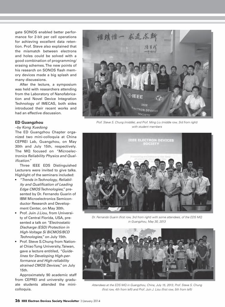
26 IEEE Electron Devices Society Newsletter ❍ January 2014
gate SONOS enabled better perfor-
mance for 2-bit per cell operations
for achieving excellent data reten-
tion. Prof. Steve also explained that
the mismatch between electrons
and holes could be solved with a
good combination of programming/
erasing schemes. The new points of
his research on SONOS flash mem-
ory devices made a big splash and
many discussions.
After the lecture, a symposium
was held with researchers attending
from the Laboratory of Nanofabrica-
tion and Novel Device Integration
Technology of IMECAS, both sides
introduced their recent works and
had an effective discussion.
ED Guangzhou–by Kong Xuedong
The ED Guangzhou Chapter orga-
nized two mini-colloquia at China
CEPREI Lab, Guangzhou, on May
30th and July 15th, respectively.
The MQ focused on “Microelec-
tronics Reliability Physics and Qual-
ification.”
Three IEEE EDS Distinguished
Lecturers were invited to give talks.
Highlight of the seminars included:
• “Trends in Technology, Reliabil-
ity and Qualification of Leading
Edge CMOS Technologies,” pre-
sented by Dr. Fernando Guarin of
IBM Microelectronics Semicon-
ductor Research and Develop-
ment Center, on May 30th.
• Prof. Juin J.Liou, from Universi-
ty of Central Florida, USA, pre-
sented a talk on “Electrostatic
Discharge (ESD) Protection in
High-Voltage Si BiCMOS/BCD
Technologies,” on July 15th.
• Prof. Steve S.Chung from Nation-
al Chiao Tung University, Taiwan,
gave a lecture entitiled, “Guide-
lines for Developing High-per-
formance and High-reliability
strained CMOS Devices,” on July
15th.
Approximately 90 academic staff
from CEPREI and university gradu-
ate students attended the mini-
colloquia.
Prof. Steve S. Chung (middle), and Prof. Ming Liu (middle row, 3rd from right) with student members
Dr. Fernando Guarin (first row, 3rd from right) with some attendees, of the EDS MQ in Guangzhou, May 30, 2013
Attendees at the EDS MQ in Guangzhou, China, July 15, 2013, Prof. Steve S. Chung (first row, 4th from left) and Prof. Juin J. Liou (first row, 5th from left)
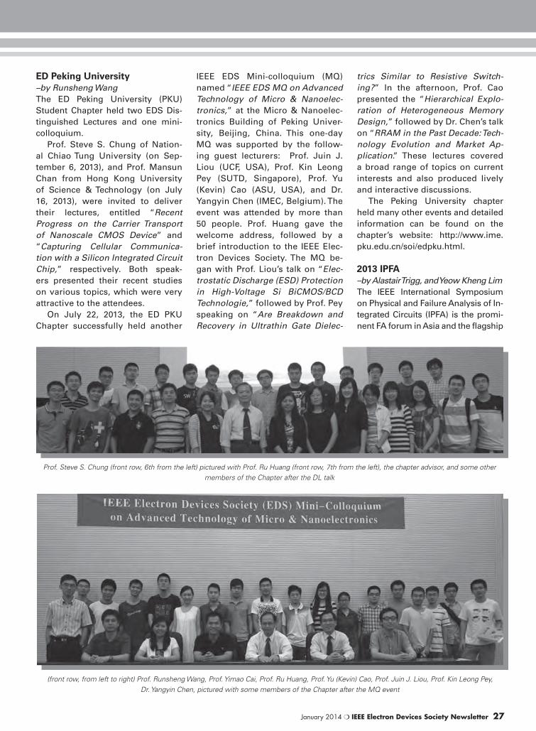
January 2014 ❍ IEEE Electron Devices Society Newsletter 27
ED Peking University–by Runsheng Wang
The ED Peking University (PKU)
Student Chapter held two EDS Dis-
tinguished Lectures and one mini-
colloquium.
Prof. Steve S. Chung of Nation-
al Chiao Tung University (on Sep-
tember 6, 2013), and Prof. Mansun
Chan from Hong Kong University
of Science & Technology (on July
16, 2013), were invited to deliver
their lectures, entitled “Recent
Progress on the Carrier Transport
of Nanoscale CMOS Device” and
“Capturing Cellular Communica-
tion with a Silicon Integrated Circuit
Chip,” respectively. Both speak-
ers presented their recent studies
on various topics, which were very
attractive to the attendees.
On July 22, 2013, the ED PKU
Chapter successfully held another
IEEE EDS Mini-colloquium (MQ)
named “IEEE EDS MQ on Advanced
Technology of Micro & Nanoelec-
tronics,” at the Micro & Nanoelec-
tronics Building of Peking Univer-
sity, Beijing, China. This one-day
MQ was supported by the follow-
ing guest lecturers: Prof. Juin J.
Liou (UCF, USA), Prof. Kin Leong
Pey (SUTD, Singapore), Prof. Yu
(Kevin) Cao (ASU, USA), and Dr.
Yangyin Chen (IMEC, Belgium). The
event was attended by more than
50 people. Prof. Huang gave the
welcome address, followed by a
brief introduction to the IEEE Elec-
tron Devices Society. The MQ be-
gan with Prof. Liou’s talk on “Elec-
trostatic Discharge (ESD) Protection
in High-Voltage Si BiCMOS/BCD
Technologie,” followed by Prof. Pey
speaking on “Are Breakdown and
Recovery in Ultrathin Gate Dielec-
trics Similar to Resistive Switch-
ing?” In the afternoon, Prof. Cao
presented the “Hierarchical Explo-
ration of Heterogeneous Memory
Design,” followed by Dr. Chen’s talk
on “RRAM in the Past Decade: Tech-
nology Evolution and Market Ap-
plication.” These lectures covered
a broad range of topics on current
interests and also produced lively
and interactive discussions.
The Peking University chapter
held many other events and detailed
information can be found on the
chapter’s website: http://www.ime.
pku.edu.cn/soi/edpku.html.
2013 IPFA–by Alastair Trigg, and Yeow Kheng Lim
The IEEE International Symposium
on Physical and Failure Analysis of In-
tegrated Circuits (IPFA) is the promi-
nent FA forum in Asia and the flagship
(front row, from left to right) Prof. Runsheng Wang, Prof. Yimao Cai, Prof. Ru Huang, Prof. Yu (Kevin) Cao, Prof. Juin J. Liou, Prof. Kin Leong Pey, Dr. Yangyin Chen, pictured with some members of the Chapter after the MQ event
Prof. Steve S. Chung (front row, 6th from the left) pictured with Prof. Ru Huang (front row, 7th from the left), the chapter advisor, and some other members of the Chapter after the DL talk
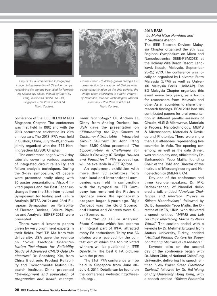
28 IEEE Electron Devices Society Newsletter ❍ January 2014
conference of the IEEE REL/CPMT/ED
Singapore Chapter. The conference
was first held in 1987, and with the
2013 occurrence celebrated its 20th
anniversary. The 2013 IPFA was held
in Suzhou, China, July 15–19, and was
jointly organized with the IEEE Nan-
jing Section ED/SSC Chapter.
The conference began with 2-day
tutorials covering various aspects
of integrated circuit reliability and
failure analysis techniques. During
the 3-day symposium, 63 papers
were presented orally along with
80 poster presentations. Also, 4 in-
vited papers and the Best Paper ex-
changes from the 38th International
Symposium for Testing and Failure
Analysis (ISTFA 2012) and 23rd Eu-
ropean Symposium on Reliability
of Electron Devices, Failure Phys-
ics and Analysis (ESREF 2012) were
presented.
There were 4 keynote papers
given by very prominent experts in
their fields. Prof. T.P. Ma from Yale
University, USA gave the keynote
on “Novel Electrical Character-
ization Techniques for Reliability
Study of Advanced CMOS Gate Di-
electrics.” Dr. Shaofeng Xie, from
China Electronic Product Reliabil-
ity and Environmental Testing Re-
search Institute, China presented
“Development and application of
prognostics and health manage-
ment technology.” Dr. Andrew H.
Olney from Analog Devices, Inc.
USA gave the presentation on
“Eliminating the Top Causes of
Customer-Attributable Integrated
Circuit Failures.” Dr. John Peng
from SMIC China presented “The
Opportunities & Challenges for
China’s Growing IC Design Houses
and Foundries.” IPFA proceedings
will be available in IEEE Xplore.
An equipment exhibition with
more than 30 exhibitors from
both local and international com-
panies was held in conjunction
with the symposium. FEI Com-
pany has remained the Platinum
Sponsor since the sponsorship
program began 6 years ago. Digit
Concept was the Gold Sponsor
and Hanwa and Wintech were Sil-
ver Sponsors.
The “Art of Failure Analysis”
Photo Contest which has become
an integral part of IPFA, attracted
many FA enthusiasts. Thirty-two FA
photos were received for the con-
test out of which the top 12 voted
winners will be published in IEEE
Spectrum. The best 6 FA pictures
won the prizes.
The 21st IPFA conference will be
held in Singapore from June 30–
July 4, 2014. Details can be found on
the conference website: http://ieee-
ipfa.org/ .
2013 RSM –by Mohd Nizar Hamidon and
P Susthitha Menon
The IEEE Electron Devices Malay-
sia Chapter organized the 9th IEEE
Regional Symposium on Micro and
Nanoelectronics (IEEE-RSM2013) at
the Holiday Villa Beach Resort, Lang-
kawi, Kedah, Malaysia, September
25–27, 2013. The conference was lo-
cally co-organized by Universiti Putra
Malaysia (UPM) as well as Univer-
siti Malaysia Perlis (UniMAP). The
ED Malaysia Chapter organizes this
event every two years, as a forum
for researchers from Malaysia and
other Asian countries to share their
research findings. RSM 2013 had 106
contributed papers for oral presenta-
tion in different parallel sessions of
Circuits, VLSI & Microwave, Materials
& Process, Nanotechnology, MEMS
& Microsensors, Materials & Devic-
es and Photonics. There were more
than 130 attendees, representing five
countries in Asia. The opening cer-
emony, as well as the gala dinner,
was held on day one, officiated by Dr.
Burhanuddin Yeop Majlis, founding
Chair of the RSM and Director of the
Institute of Microengineering and Na-
noelectronics (IMEN) UKM.
Day one of the conference had
three keynote speakers: Dr. MK.
Radhakrishnan, of NanoRel deliv-
ered a talk entitled “Analysis Chal-
lenges and Interface Physics in
Silicon Nanodevices,” followed by
Dr. Burhanuddin Yeop Majlis, the Di-
rector of IMEN, UKM, who delivered
a speech entitled “MEMS and Lab
on Chip: Interfacing Macro to Nano
World.” The session ended with a
keynote by Dr. Mehmet Ertugrul from
Ataturk University, Turkey, entitled
“Artificial Pinning Centers for Super-
conducting Microwave Resonators.”
Keynote talks on the second
day of the conference began with
Dr. Albert Chin, of National Chiao Tung
University, delivering his speech en-
titled “Low Power Green Electronic
Devices,” followed by Dr. Hei Wong
of City University Hong Kong, with
a speech entitled “Silicon Photonics
X ray 3D CT (Computerised Tomography) image during inspection of C4 solder bumps
resembling the storage pots used for ferment-ing Korean soy sauce. Picture by Chew Su
Fang, Xilinx Asia Pacific Pte. Ltd., Singapore – 1st Prize in Art of FA
Photo Contest.
Fir Tree Green - Suddenly grown during a FIB cross section by a reaction of Ga-ions with
some contamination on the chip surface; the image taken afterwards in a SEM. Picture
by Neumann, Infineon Technologies, Munich Germany – 2nd Prize in Art of FA
Photo Contest.
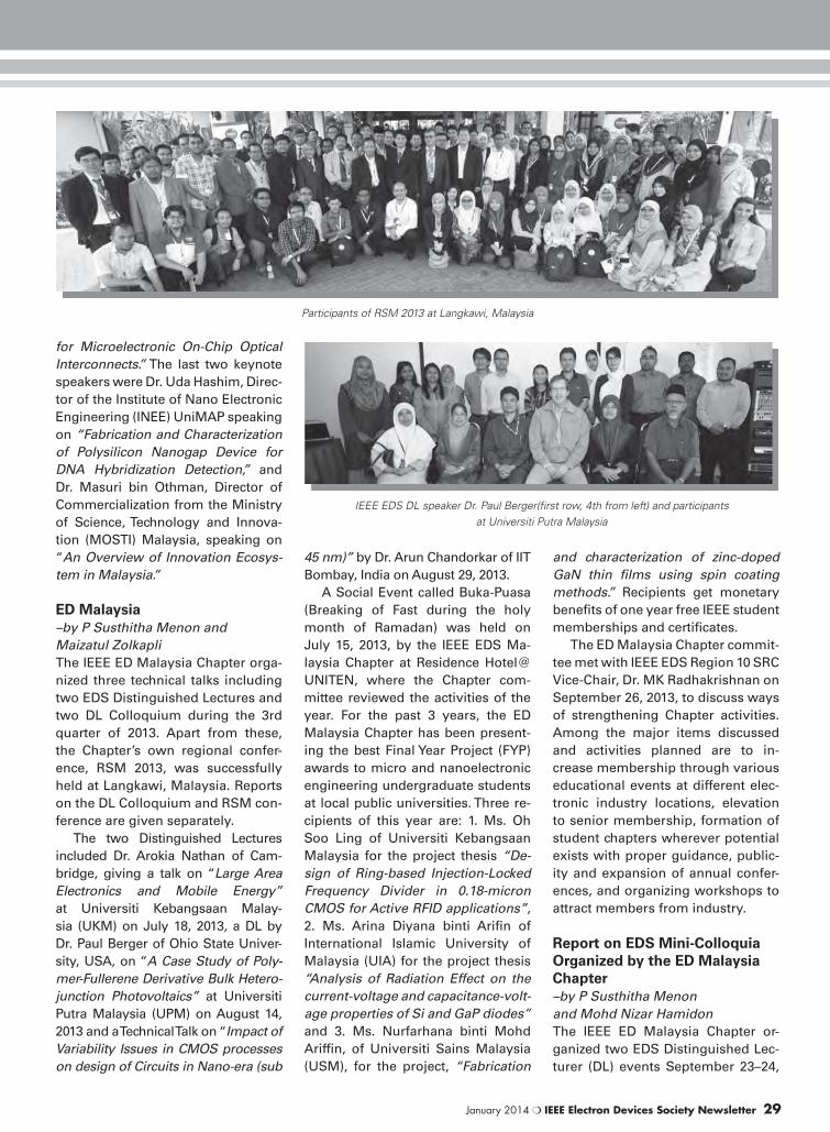
January 2014 ❍ IEEE Electron Devices Society Newsletter 29
for Microelectronic On-Chip Optical
Interconnects.” The last two keynote
speakers were Dr. Uda Hashim, Direc-
tor of the Institute of Nano Electronic
Engineering (INEE) UniMAP speaking
on “Fabrication and Characterization
of Polysilicon Nanogap Device for
DNA Hybridization Detection,” and
Dr. Masuri bin Othman, Director of
Commercialization from the Ministry
of Science, Technology and Innova-
tion (MOSTI) Malaysia, speaking on
“An Overview of Innovation Ecosys-
tem in Malaysia.”
ED Malaysia–by P Susthitha Menon and
Maizatul Zolkapli
The IEEE ED Malaysia Chapter orga-
nized three technical talks including
two EDS Distinguished Lectures and
two DL Colloquium during the 3rd
quarter of 2013. Apart from these,
the Chapter’s own regional confer-
ence, RSM 2013, was successfully
held at Langkawi, Malaysia. Reports
on the DL Colloquium and RSM con-
ference are given separately.
The two Distinguished Lectures
included Dr. Arokia Nathan of Cam-
bridge, giving a talk on “Large Area
Electronics and Mobile Energy”
at Universiti Kebangsaan Malay-
sia (UKM) on July 18, 2013, a DL by
Dr. Paul Berger of Ohio State Univer-
sity, USA, on “A Case Study of Poly-
mer-Fullerene Derivative Bulk Hetero-
junction Photovoltaics” at Universiti
Putra Malaysia (UPM) on August 14,
2013 and a Technical Talk on “Impact of
Variability Issues in CMOS processes
on design of Circuits in Nano-era (sub
45 nm)” by Dr. Arun Chandorkar of IIT
Bombay, India on August 29, 2013.
A Social Event called Buka-Puasa
(Breaking of Fast during the holy
month of Ramadan) was held on
July 15, 2013, by the IEEE EDS Ma-
laysia Chapter at Residence Hotel@
UNITEN, where the Chapter com-
mittee reviewed the activities of the
year. For the past 3 years, the ED
Malaysia Chapter has been present-
ing the best Final Year Project (FYP)
awards to micro and nanoelectronic
engineering undergraduate students
at local public universities. Three re-
cipients of this year are: 1. Ms. Oh
Soo Ling of Universiti Kebangsaan
Malaysia for the project thesis “De-
sign of Ring-based Injection-Locked
Frequency Divider in 0.18-micron
CMOS for Active RFID applications”,
2. Ms. Arina Diyana binti Arifin of
International Islamic University of
Malaysia (UIA) for the project thesis
“Analysis of Radiation Effect on the
current-voltage and capacitance-volt-
age properties of Si and GaP diodes”
and 3. Ms. Nurfarhana binti Mohd
Ariffin, of Universiti Sains Malaysia
(USM), for the project, “Fabrication
and characterization of zinc-doped
GaN thin films using spin coating
methods.” Recipients get monetary
benefits of one year free IEEE student
memberships and certificates.
The ED Malaysia Chapter commit-
tee met with IEEE EDS Region 10 SRC
Vice-Chair, Dr. MK Radhakrishnan on
September 26, 2013, to discuss ways
of strengthening Chapter activities.
Among the major items discussed
and activities planned are to in-
crease membership through various
educational events at different elec-
tronic industry locations, elevation
to senior membership, formation of
student chapters wherever potential
exists with proper guidance, public-
ity and expansion of annual confer-
ences, and organizing workshops to
attract members from industry.
Report on EDS Mini-Colloquia Organized by the ED Malaysia Chapter –by P Susthitha Menon
and Mohd Nizar Hamidon
The IEEE ED Malaysia Chapter or-
ganized two EDS Distinguished Lec-
turer (DL) events September 23–24,
Participants of RSM 2013 at Langkawi, Malaysia
IEEE EDS DL speaker Dr. Paul Berger(first row, 4th from left) and participants at Universiti Putra Malaysia
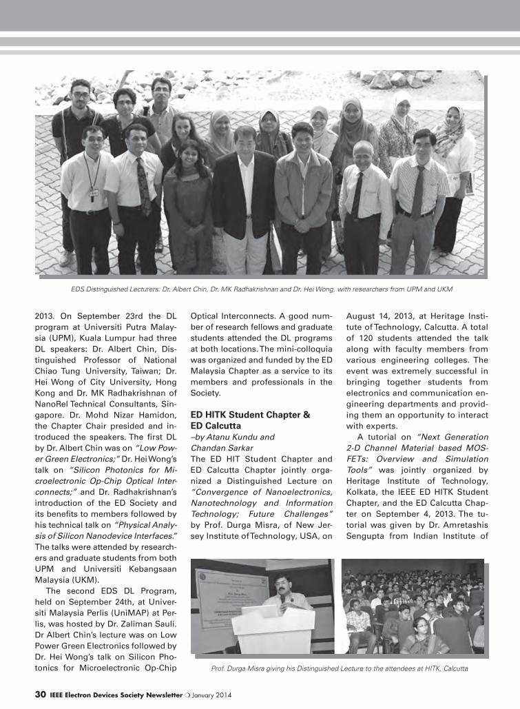
30 IEEE Electron Devices Society Newsletter ❍ January 2014
2013. On September 23rd the DL
program at Universiti Putra Malay-
sia (UPM), Kuala Lumpur had three
DL speakers: Dr. Albert Chin, Dis-
tinguished Professor of National
Chiao Tung University, Taiwan; Dr.
Hei Wong of City University, Hong
Kong and Dr. MK Radhakrishnan of
NanoRel Technical Consultants, Sin-
gapore. Dr. Mohd Nizar Hamidon,
the Chapter Chair presided and in-
troduced the speakers. The first DL
by Dr. Albert Chin was on “Low Pow-
er Green Electronics;” Dr. Hei Wong’s
talk on “Silicon Photonics for Mi-
croelectronic Op-Chip Optical Inter-
connects;” and Dr. Radhakrishnan’s
introduction of the ED Society and
its benefits to members followed by
his technical talk on “Physical Analy-
sis of Silicon Nanodevice Interfaces.”
The talks were attended by research-
ers and graduate students from both
UPM and Universiti Kebangsaan
Malaysia (UKM).
The second EDS DL Program,
held on September 24th, at Univer-
siti Malaysia Perlis (UniMAP) at Per-
lis, was hosted by Dr. Zaliman Sauli.
Dr Albert Chin’s lecture was on Low
Power Green Electronics followed by
Dr. Hei Wong’s talk on Silicon Pho-
tonics for Microelectronic Op-Chip
Optical Interconnects. A good num-
ber of research fellows and graduate
students attended the DL programs
at both locations. The mini-colloquia
was organized and funded by the ED
Malaysia Chapter as a service to its
members and professionals in the
Society.
ED HITK Student Chapter & ED Calcutta–by Atanu Kundu and
Chandan Sarkar
The ED HIT Student Chapter and
ED Calcutta Chapter jointly orga-
nized a Distinguished Lecture on
“Convergence of Nanoelectronics,
Nanotechnology and Information
Technology; Future Challenges”
by Prof. Durga Misra, of New Jer-
sey Institute of Technology, USA, on
August 14, 2013, at Heritage Insti-
tute of Technology, Calcutta. A total
of 120 students attended the talk
along with faculty members from
various engineering colleges. The
event was extremely successful in
bringing together students from
electronics and communication en-
gineering departments and provid-
ing them an opportunity to interact
with experts.
A tutorial on “Next Generation
2-D Channel Material based MOS-
FETs: Overview and Simulation
Tools” was jointly organized by
Heritage Institute of Technology,
Kolkata, the IEEE ED HITK Student
Chapter, and the ED Calcutta Chap-
ter on September 4, 2013. The tu-
torial was given by Dr. Amretashis
Sengupta from Indian Institute of
Prof. Durga Misra giving his Distinguished Lecture to the attendees at HITK, Calcutta
EDS Distinguished Lecturers: Dr. Albert Chin, Dr. MK Radhakrishnan and Dr. Hei Wong, with researchers from UPM and UKM
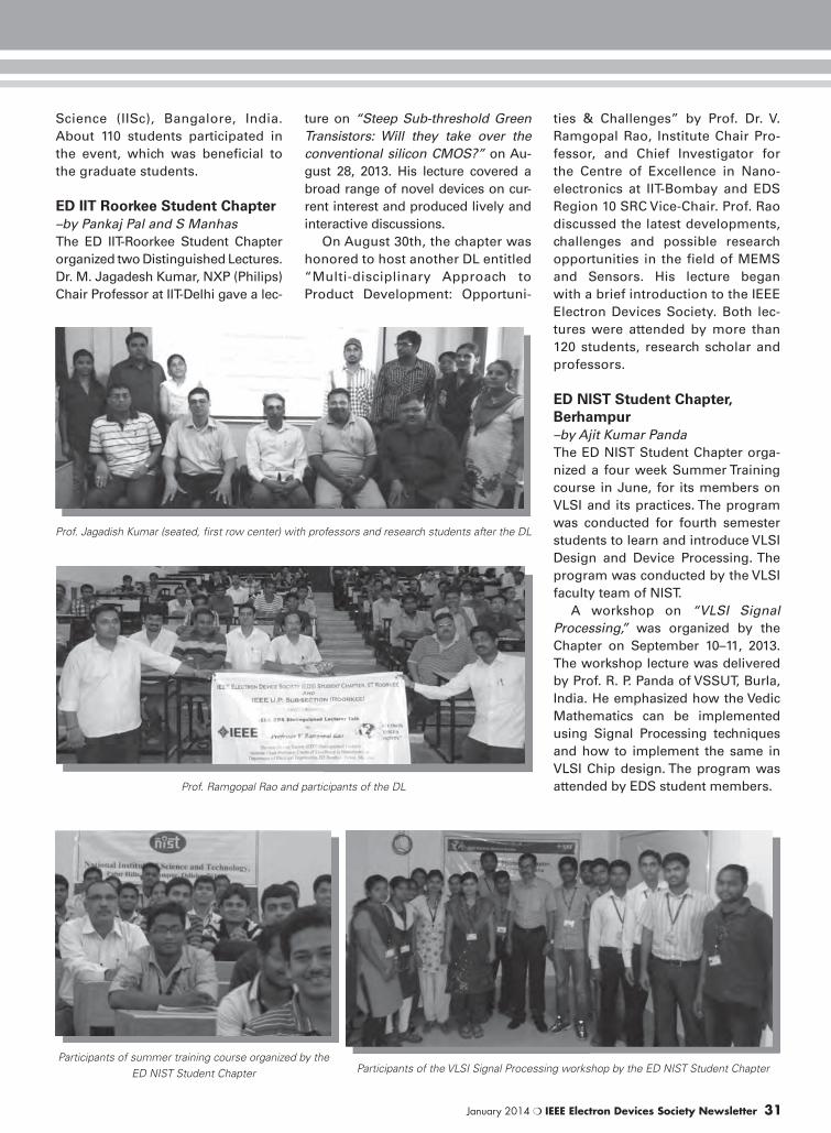
January 2014 ❍ IEEE Electron Devices Society Newsletter 31
Science (IISc), Bangalore, India.
About 110 students participated in
the event, which was beneficial to
the graduate students.
ED IIT Roorkee Student Chapter–by Pankaj Pal and S Manhas
The ED IIT-Roorkee Student Chapter
organized two Distinguished Lectures.
Dr. M. Jagadesh Kumar, NXP (Philips)
Chair Professor at IIT-Delhi gave a lec-
ture on “Steep Sub-threshold Green
Transistors: Will they take over the
conventional silicon CMOS?” on Au-
gust 28, 2013. His lecture covered a
broad range of novel devices on cur-
rent interest and produced lively and
interactive discussions.
On August 30th, the chapter was
honored to host another DL entitled
“Multi-disciplinary Approach to
Product Development: Opportuni-
ties & Challenges” by Prof. Dr. V.
Ramgopal Rao, Institute Chair Pro-
fessor, and Chief Investigator for
the Centre of Excellence in Nano-
electronics at IIT-Bombay and EDS
Region 10 SRC Vice-Chair. Prof. Rao
discussed the latest developments,
challenges and possible research
opportunities in the field of MEMS
and Sensors. His lecture began
with a brief introduction to the IEEE
Electron Devices Society. Both lec-
tures were attended by more than
120 students, research scholar and
professors.
ED NIST Student Chapter, Berhampur –by Ajit Kumar Panda
The ED NIST Student Chapter orga-
nized a four week Summer Training
course in June, for its members on
VLSI and its practices. The program
was conducted for fourth semester
students to learn and introduce VLSI
Design and Device Processing. The
program was conducted by the VLSI
faculty team of NIST.
A workshop on “VLSI Signal
Processing,” was organized by the
Chapter on September 10–11, 2013.
The workshop lecture was delivered
by Prof. R. P. Panda of VSSUT, Burla,
India. He emphasized how the Vedic
Mathematics can be implemented
using Signal Processing techniques
and how to implement the same in
VLSI Chip design. The program was
attended by EDS student members.
Participants of the VLSI Signal Processing workshop by the ED NIST Student ChapterParticipants of summer training course organized by the
ED NIST Student Chapter
Prof. Ramgopal Rao and participants of the DL
Prof. Jagadish Kumar (seated, first row center) with professors and research students after the DL
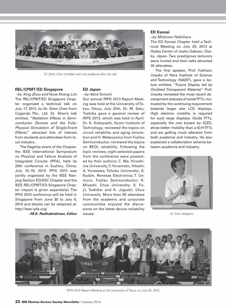
32 IEEE Electron Devices Society Newsletter ❍ January 2014
REL/CPMT/ED Singapore–by Xing Zhou and Yeow Kheng Lim
The REL/CPMT/ED Singapore Chap-
ter organized a technical talk on
July 17, 2013, by Dr. Shen Chen from
Cogenda Pte., Ltd. Dr. Shen’s talk
entitled, “Radiation Effects in Semi-
conductor Devices and the Fully-
Physical Simulation of Single-Event
Effects,” attracted lots of interest
from students and attendees from lo-
cal industry.
The flagship event of the Chapter,
the IEEE International Symposium
on Physical and Failure Analysis of
Integrated Circuits (IPFA), held its
20th conference in Suzhou, China,
July 15–19, 2013. IPFA 2013 was
jointly organized by the IEEE Nan-
jing Section ED/SSC Chapter and the
IEEE REL/CPMT/ED Singapore Chap-
ter (report is given separately). The
IPFA 2014 conference will be held in
Singapore from June 30 to July 4,
2014 and details can be obtained at:
http://ieee-ipfa.org/
~M.K. Radhakrishnan, Editor
ED Japan–by Akira Toriumi
Our annual IRPS 2013 Report Meet-
ing was held at the University of To-
kyo, Tokyo, July 25th. Dr. M. Sato,
Toshiba gave a general review of
IRPS 2013, which was held in April.
Dr. K. Kobayashi, Kyoto Institute of
Technology, reviewed the topics on
circuit reliability and aging simula-
tion and H. Matsuyama from Fujitsu
Semiconductor, reviewed the topics
on BEOL reliability. Following the
topic reviews, eight selected papers
from the conference were present-
ed by their authors: C. Ma, Hiroshi-
ma University; Y. Yonamoto, Hitachi;
A. Yonezawa, Tohoku University; S.
Kudoh, Renesas Electronics; T. Ue-
mura, Fujitsu Semiconductor; K.
Miyachi, Chuo University; S. Fu-
jii, Toshiba; and K. Joguchi, Chuo
University. More than 60 attendees
from the academic and corporate
communities enjoyed the discus-
sions on the latest device reliability
issues.
ED Kansai–by Michinori Nishihara
The ED Kansai Chapter held a Tech-
nical Meeting on July 29, 2013 at
Osaka Center of Josho Gakuen, Osa-
ka, Japan. Two prestigious lecturers
were invited and their talks attracted
30 attendees.
The first speaker, Prof. Yukiharu
Uraoka of Nara Institute of Science
and Technology (NAIST), gave a lec-
ture entitled, “Future Display led by
Oxidized Transparent Material.” Prof.
Uraoka reviewed the most recent de-
velopment statuses of oxide TFTs, mo-
tivated by the continuing requirement
towards larger size LCD displays.
High electron mobility is required
for such large displays. Oxide TFTs,
especially the one known by IGZO,
show better mobility than a-Si:H TFTs
and are getting much attention from
both academia and industry. He also
explained a collaboration scheme be-
tween academia and industry.
Dr. Tohru Mogami
IRPS 2013 Report Meeting at the University of Tokyo, on July 25, 2013
Dr. Shen Chen (middle) with the audience after the talk

January 2014 ❍ IEEE Electron Devices Society Newsletter 33
The second lecturer, Dr. Tohru Mo-
gami of Photonics Electronics Technol-
ogy Research Association (PETRA),
gave his talk entitled, “Si-LSI Innova-
tions and Challenge.” Before explain-
ing development trends of various
FETs, he discussed a recent difficult
situation of Japanese semiconduc-
tor companies. Based on his industry
background, he gave his ideas on why
it happened and how to improve the
situation. His lecture was very thought
provoking and encouraged young stu-
dents to pursue their career.
The next event hosted by the ED
Kansai Chapter will be the IEDM 2013
feedback meeting, scheduled for Janu-
ary 2014. Please check our chapter’s
website for more details: http://www.
ieee-jp.org/section/kansai/chapter/eds/.
~ Kuniyuki Kakushima, EditorProf. Yukiharu Uraoka
Attendees of the ED Kansai Chapter Technical Meeting
34 IEEE Electron Devices Society Newsletter ❍ January 2014
THE COMPLETE EDS CALENDAR CAN BE FOUND AT OUR WEB SITE: HTTP://EDS.IEEE.ORG. PLEASE VISIT.
EDS MEET INGS CALENDAR(A S O F 06 N O V E M B E R 2013 )
24 Mar - 27 Mar 20142014 International Conference onMicroelectronic Test Structures (ICMTS)Conf Record :32659Location: Udine , ItalyContact : Francesco DriussiTel : +39 0432 558295Fax : +39 0432 558251E-mail: [email protected] : 13 Jan 2014www : http://icmts2014.uniud.it
08 Jun - 13 Jun 20142014 IEEE 40th Photovoltaic SpecialistsConference (PVSC)Conf Record :21196Location: Denver CO , USAContact : Richard R. KingTel : +1 818 838 7404Fax : +1 818 838 7474E-mail: [email protected] : 26 May 2014www : http://www.ieee-pvsc.org/PVSC40
09 Sep - 11 Sep 20142014 International Conference onSimulation of Semiconductor Processesand Devices (SISPAD)Conf Record :32888Location: Yokohama , JapanContact : Akira HirokiTel : +81-75-724-7419Fax :E-mail: [email protected] :www : http://sites.google.com/site/sispad2014/
18 Apr - 18 Apr 20142014 IEEE Workshop OnMicroelectronics And Electron Devices(WMED)Conf Record :32556Location: Boise ID , USAContact : Jaydeb GoswamiTel :Fax :E-mail: [email protected] : 17 Feb 2014www : http://www.ewh.ieee.org/r6/boise/wmed2014/WMED2014.html
08 Jun - 09 Jun 20142014 Silicon Nanoelectronics Workshop(SNW)Conf Record :32907Location: Honolulu HI , USAContact : Simon DeleonibusTel : +33 673518545Fax :E-mail: [email protected] :www : http://
14 Sep - 17 Sep 20142014 IEEE Custom Integrated CircuitsConference - CICC 2014Conf Record :18693Location: San Jose CA , USAContact : Melissa WiderkehrTel : +1 301 527 0900Fax : +1 301 527 0994E-mail: [email protected] :www : http://www.ieee-cicc.org
22 Apr - 24 Apr 20142014 IEEE International VacuumElectronics Conference (IVEC)Conf Record :20241Location: Monterey CA , USAContact : Mark GoldfarbTel : 212-460-9700Fax :E-mail: [email protected] :www : http://
10 Jun - 12 Jun 20142014 IEEE Symposium on VLSITechnologyConf Record :18214Location: Honolulu HI , USAContact : Phyllis MahoneyTel : +1 301 527 0900Fax : +1 301 527 0994E-mail: [email protected] :www : http://www.vlsisymposium.org
28 Sep - 01 Oct 20142014 IEEE Bipolar/BiCMOS Circuits andTechnology Meeting - BCTMConf Record :31342Location: Chicago IL , USAContact : Catherine ShawTel : 404-385-3555Fax :E-mail: [email protected] : 18 Jul 2014www : http://ieee-bctm.org/
28 Apr - 30 Apr 20142014 International Symposium on VLSITechnology, Systems and Application(VLSI-TSA)Conf Record :32546Location: Hsinchu , TaiwanContact : Jenny LinTel : +886 3-5916705Fax : +886 3-5820221E-mail: [email protected] : 31 Oct 2013www : http://vlsitsa.itri.org.tw/
15 Jun - 17 Jun 20142014 20th BiennialUniversity/Government/IndustryMicro/Nano Symposium (UGIM)Conf Record :32966Location: Cambridge MA , USAContact : Eric MartinTel : +1 617-495-3161Fax :E-mail: [email protected] : 30 May 2014www : http://www.cns.fas.harvard.edu/UGIM2014/index.php
29 Sep - 03 Oct 20142014 25th European Symposium onReliability of Electron Devices, FailurePhysics and Analysis (ESREF)Conf Record :32961Location: Berlin , GermanyContact : Jasmin KayadelenTel : +49 69 6308275Fax : +49 69 6308144E-mail: [email protected] : 06 Jun 2014www : http://www.esref2014.org
28 Apr - 30 Apr 20142014 International Symposium on VLSIDesign, Automation and Test (VLSI-DAT)Conf Record :32530Location: Hsinchu , TaiwanContact : Elodie HoTel : +886-3-5919039Fax :E-mail: [email protected] : 31 Jan 2014www : http://vlsidat.itri.org.tw/
15 Jun - 19 Jun 20142014 IEEE 26th InternationalSymposium on Power SemiconductorDevices & IC's (ISPSD)Conf Record :20170Location: Waikoloa HI , USAContact : Don DisneyTel : +1 408 684 5223Fax :E-mail: [email protected] : 08 Mar 2014www : http://www.ispsd2014.com
06 Oct - 09 Oct 20142014 IEEE SOI-3D-SubthresholdMicroelectronics Technology UnifiedConference (S3S)Conf Record :33072Location: San Francisco CA , USAContact : Joyce LloydTel : 818-795-3762Fax : 818-855-8392E-mail: [email protected] :www : http://http://s3sconference.org/
January 2014 ❍ IEEE Electron Devices Society Newsletter 35
18 May - 21 May 20142014 IEEE 6th International MemoryWorkshop (IMW)Conf Record :32432Location: Taipei , TaiwanContact : Pei-Ying DuTel : +886955-986-685Fax : +8863-578-9087E-mail: [email protected] :www : http://
18 Jun - 20 Jun 20142014 IEEE International Conference onElectron Devices and Solid-State Circuits(EDSSC)Conf Record :32286Location: Chengdu , ChinaContact : Zhiwei LiuTel : +86-28-83201281Fax :E-mail: [email protected] : 31 Mar 2014www : http://www.edssc2014.com
13 Oct - 14 Oct 2014INTERNATIONAL CONFERENCE ONCOMMUNICATION & NANO TECHNOLOGYConf Record :31570Location: CHENNAI , IndiaContact : Arun prasadTel : +919865413635Fax :E-mail: [email protected] : 06 Sep 2013www : http://WWW.ICCNT-ECE.ORG
19 May - 21 May 20142014 25th Annual SEMI AdvancedSemiconductor ManufacturingConference (ASMC)Conf Record :32974Location: Saratoga Springs NY , USAContact : Margaret KindlingTel : +1-202-393-5552Fax :E-mail: [email protected] : 28 Apr 2014www : http://www.semi.org/asmc2014
22 Jun - 25 Jun 20142014 72nd Annual Device ResearchConference (DRC)Conf Record :32941Location: Santa Barbara CA , USAContact : Ioannis KymissisTel : 3478500235Fax :E-mail: [email protected] : 15 Apr 2013www : http://www.drc.ee.psu.edu/
19 Oct - 22 Oct 20142014 IEEE Compound SemiconductorIntegrated Circuit Symposium (CSISC)Conf Record :31991Location: San Diego CA , USAContact : Douglas McPhersonTel : +1 613-670-3371Fax :E-mail: [email protected] : 25 Jul 2014www : http://www.csics.org
20 May - 23 May 20142014 IEEE Internatioal InterrconnectTechnology Conferencei/AdvancedMetallization Conference (IITC/AMC)Conf Record :32991Location: San Jose CA , USAContact : Wendy WalkerTel : +1-301-527-0900Fax :E-mail: [email protected] : 01 Feb 2013www : http://www.his.com/~iitc
28 Jul - 31 Jul 20142014 IEEE International NanoelectronicsConference (INEC)Conf Record :31843Location: Sapporo , JapanContact : Kazuhiko EndoTel : +81-29-861-3857Fax :E-mail: [email protected] : 31 May 2014www : http://
10 Dec - 13 Dec 20142014 IEEE 45th Semiconductor InterfaceSpecialists Conference (SISC)Conf Record :31578Location: San Diego CA , USAContact : Alex DemkovTel : +1 512 471 8560Fax :E-mail: [email protected] : 20 Aug 2014www : http://www.ieeesisc.org/
27 May - 30 May 20142014 International Conference onelectron, Ion, and Photon BeamTechnology and Nanofabrication(EIPBN)Conf Record :32742Location: Washington DC , USAContact : Theodore FedynyshynTel : +1-781-981-7811Fax : +1-781-981-4983E-mail: [email protected] : 31 Jul 2014www : http://eipbn.org/
05 Aug - 07 Aug 20142014 Lester Eastman Conference (LFE)Conf Record :32909Location: Ithaca NY , USAContact : Pane ChaoTel : 6038856695Fax :E-mail: [email protected] : 22 Aug 2014www : http://www.leconf.com
11 Dec - 19 Dec 20142014 IEEE International ElectronDevices Meeting (IEDM)Conf Record :11149Location: San Francisco CA , USAContact : Ms. Phyllis W. MahoneyTel : +1 301 527 0900 (Ext.103)Fax : +1 301 527 0994E-mail: [email protected] :www : http://
31 May - 05 Jun 20142014 IEEE International ReliabilityPhysics Symposium (IRPS)Conf Record :20379Location: Waikoloa HI , USAContact : David BarberTel : +1 828 898 7001Fax : +1 828 898 6375E-mail: [email protected] :www : http://www.irps.org
01 Sep - 05 Sep 20142014 29th Symposium onMicroelectronics Technology and Devices(SBMicro)Conf Record :33078Location: Aracaju , BrazilContact : Edward David MorenoTel : +55 79 9198-4939Fax :E-mail: [email protected] : 01 Jun 2014www : http://www.sbmicro.org.br/sbmicro
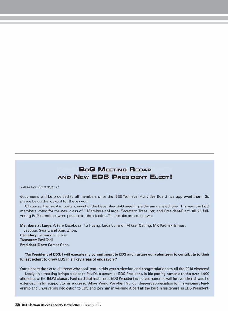
36 IEEE Electron Devices Society Newsletter ❍ January 2014
documents will be provided to all members once the IEEE Technical Activities Board has approved them. So
please be on the lookout for these soon.
Of course, the most important event of the December BoG meeting is the annual elections. This year the BoG
members voted for the new class of 7 Members-at-Large, Secretary, Treasurer, and President-Elect. All 25 full-
voting BoG members were present for the election. The results are as follows:
Members at Large: Arturo Escobosa, Ru Huang, Leda Lunardi, Mikael Ostling, MK Radhakrishnan,
Jacobus Swart, and Xing Zhou.
Secretary: Fernando Guarin
Treasurer: Ravi Todi
President-Elect: Samar Saha
“As President of EDS, I will execute my commitment to EDS and nurture our volunteers to contribute to their fullest extent to grow EDS in all key areas of endeavors.”
Our sincere thanks to all those who took part in this year’s election and congratulations to all the 2014 electees!
Lastly, this meeting brings a close to Paul Yu’s tenure as EDS President. In his parting remarks to the over 1,000
attendees of the IEDM plenary Paul said that his time as EDS President is a great honor he will forever cherish and he
extended his full support to his successor Albert Wang. We offer Paul our deepest appreciation for his visionary lead-
ership and unwavering dedication to EDS and join him in wishing Albert all the best in his tenure as EDS President.
BOG MEETING RECAP AND NEW EDS PRESIDENT ELECT!
(continued from page 1)