table of contents - imda
TRANSCRIPT
I n f o c o m m T e c h n o l o g y R o a d m a p R e l e a s e F e b r u a r y 2 0 0 2
i
Table Of ContentsACKNOWLEDGEMENTS...................................................................................................................... III
EXECUTIVE SUMMARY..........................................................................................................................V
1 INTRODUCTION...............................................................................................................................11.1 OBJECTIVE ......................................................................................................................................... 11.2 DRIVERS FOR NEXT GENERATION OPTICAL NETWORKS ....................................................................................... 21.3 CHALLENGES & BENEFITS FOR NETWORK OPERATORS ........................................................................................ 3
2 NEXT GENERATION OPTICAL NETWORKS.......................................................................................52.1 ATTRIBUTES OF THE DIFFERENT NETWORK SEGMENTS........................................................................................ 5
2.1.1 Long-Haul Network...................................................................................................................................5 2.1.2 Metropolitan Area Network........................................................................................................................7 2.1.3 Access Network........................................................................................................................................8
2.2 OPTICAL NETWORK EVOLUTION ................................................................................................................. 8 2.2.1 SONET/SDH Networks ..............................................................................................................................9 2.2.2 Architecture of Existing Optical Networks ................................................................................................. 10 2.2.3 Architecture of Next Generation Optical Network, Issues and Challenges .................................................... 13
2.3 STANDARD DEVELOPMENTS..................................................................................................................... 18 2.3.1 ITU-T .................................................................................................................................................... 18 2.3.2 IETF ...................................................................................................................................................... 22 2.3.3 Automatic Switched Optical Network (ASON) and Automatic Switched Transport Network (ASTN) ................ 24 2.3.4 Optical Internetworking Forum (OIF) ....................................................................................................... 26 2.3.5 Optical Domain Service Interconnect (ODSI) ............................................................................................ 27 2.3.6 IEEE Standard Development on Gigabit Ethernet & Resilient Packet Ring.................................................... 27 2.3.7 ITU Standards Development on Passive Optical Network (PON) ................................................................. 30
3 PHOTONICS ENABLING TECHNOLOGIES .......................................................................................353.1 OPTICAL TRANSPORT SYSTEM TECHNOLOGIES ............................................................................................... 37
3.1.1 DWDM................................................................................................................................................... 37 3.1.2 Soliton Transmission ............................................................................................................................... 40 3.1.3 Optical Regeneration .............................................................................................................................. 41
3.2 ACTIVE COMPONENTS & SUB-SYSTEMS....................................................................................................... 42 3.2.1 Lasers ................................................................................................................................................... 42 3.2.2 Optical Ampliers ................................................................................................................................... 45 3.2.3 Optical Switching.................................................................................................................................... 48
3.3 PASSIVE COMPONENTS & SUB-SYSTEMS...................................................................................................... 55 3.3.1 Connectors ............................................................................................................................................ 56 3.3.2 Dispersion Compensators ........................................................................................................................ 57 3.3.3 Optical Filters ......................................................................................................................................... 60 3.3.4 Optical Fibres ......................................................................................................................................... 58
3.4 ADVANCED OPTICAL & MEMS PACKAGING AND AUTOMATED MANUFACTURING ......................................................... 63 3.4.1 Optical-Electronic (OE) Integration........................................................................................................... 63 3.4.2 Thermal Solutions for Optical Components ............................................................................................... 65 3.4.3 Optical Packaging Materials ..................................................................................................................... 66 3.4.4 Optical Assembly and Reliability Testing ................................................................................................... 67 3.4.5 MEMS Packaging Issues and Challenges................................................................................................... 68
4 SINGAPORE LANDSCAPE................................................................................................................714.1 TELECOMMUNICATION INDUSTRY ............................................................................................................... 714.2 RESEARCH COMMUNITY ......................................................................................................................... 734.3 GOVERNMENT AGENCIES ........................................................................................................................ 74
5 CONCLUSION..................................................................................................................................79
ANNEX A. OPTICAL NETWORKING IN OTHER COUNTRIES................................................................83A.1 CANADA ............................................................................................................................................. 83A.2 CHINA............................................................................................................................................... 84A.3 EUROPE ............................................................................................................................................. 84A.4 JAPAN ............................................................................................................................................... 86A.5 KOREA .............................................................................................................................................. 86A.6 USA ................................................................................................................................................ 86
ANNEX B. MAJOR SUBMARINE CABLE NETWORKS LINKING SINGAPORE ........................................89
ANNEX C. LOCAL RESEARCH INSTITUTIONS & CENTRES..................................................................93
GLOSSARY ..........................................................................................................................................97
SURVEY FORM ..................................................................................................................................105
TA
BLE
OF C
ON
TE
NT
S
I n f o c o m m T e c h n o l o g y R o a d m a p R e l e a s e F e b r u a r y 2 0 0 2
ii
NEXT GENERATION OPTICAL NETWORKS & PHOTONICS
List of Figures and Tables
Figure 1. Multi-layer Structure of Existing Networks................................................................10Figure 2. Evolution of Optical Networks in Long-Haul.............................................................16Figure 3. Evolution of Optical Networks in MAN.....................................................................17Figure 4. Layered Structure of OTN.....................................................................................20Figure 5. Conceptual View of OTN.........................................................................................21Figure 6. Digital Wrapper.....................................................................................................21Figure 7. IETF Optical Internetwork Model............................................................................22Figure 8. ASON/ASTN Global Architecture.............................................................................24Figure 9. The Three Planes and Interfaces dened in ASON/ASTN Architecture.........................25Figure 10. Timeline for 10-Gigabit Ethernet Standard................................................................28Figure 11. Timeline for 802.17 Resilient Packet Ring.................................................................29Figure 12. Timeline for Ethernet in the First Mile......................................................................32Figure 13. Functional Block Diagram for Optical Communication Systems...................................35Figure 14. Technology Classication.......................................................................................36Figure 15. R&D & Commercialisation toward Higher Transmission Capacity.................................37Figure 16. Development scenario of commercial WDM Systems.................................................39Figure 17. Typical Fibre Attenuation Characteristics..................................................................60Figure 18. Optical Assembly Time Requirement vs Alignment Tolerance.....................................67Figure 19. Optical Product Vendors in Singapore......................................................................72
Table 1. ITU-T Recommendations for Optical Network...........................................................18Table 2. Related Work-in-Progress ITU Recommendations......................................................24Table 3. OIF Implementation Agreements on VSR................................................................25Table 4. BPON Standards Development................................................................................30Table 5. Types of Tunable Laser Technologies.......................................................................43Table 6. The Changing Face of Switching Technologies.........................................................50Table 7. Comparison between Optical Switching Technologies................................................53Table 8. Market Players in Optical Switching........................................................................54Table 9. Characteristic of Optical Fibre Types.......................................................................61Table 10. Dening Optical Packaging Hierarchy and Levels of Interconnects..............................64Table 11. Different Crystal Materials for Active Interconnects in Optical Systems........................66Table 12. MEMS Packaging Methodology and Challenges........................................................69
I n f o c o m m T e c h n o l o g y R o a d m a p R e l e a s e F e b r u a r y 2 0 0 2
iii
AcknowledgementsWe would like to thank the following organisations and individuals for their participation in interviews and the drafting of Track 1: NEXT GENERATION OPTICAL NETWORKS AND PHOTONICS of the 3rd Infocomm Technology Roadmap (ITR-3) report.
1. Dr Wong Woon Kwong Agency for Science, Technology And Research (A*STAR) 2. Mr Jasbir Singh Agency for Science, Technology And Research (A*STAR)3. Dr Wang Wei Guo Alcatel4. Mr Tham Wai Hoong Alcatel5. Dr Ivan Tam Alcatel6. Mr Wilson Toh Alcatel7. Mr Daniel C. Hu Blue Sky Research8. Dr Chak Leung Blue Sky Research9. Mr Eddie Lim Blue Sky Systems 10. Dr Cheng Xiangyin Blue Sky Systems 11. Mr Ong Peng Chuan Bragg Photonics 12. Mr Richard Chan Bragg Photonics 13. Mr Rodney Kee Tien Yew Cisco Systems14. Mr Yap Hak Huen Cisco Systems15. Mr Jason Chia Economic Development Board (EDB)16. Mr Low Wei Shing Economic Development Board (EDB)17. Ms Cheryl Lim Economic Development Board (EDB)18. Dr Fang Zhong Ping GINTIC Institute of Manufacturing Technology19. Dr Wang Zhiping GINTIC Institute of Manufacturing Technology20. Dr Lim Gnian Cher GINTIC Institute of Manufacturing Technology21. Mr Lai Fook Ngian Infocomm Development Authority of Singapore (IDA)22. Mr Ivan Au Infocomm Development Authority of Singapore (IDA)23. Mr Ong Kian Lin Infocomm Development Authority of Singapore (IDA)24. Mr Lua Eng Keong Infocomm Development Authority of Singapore (IDA)25. Dr Kripesh Vaidyanathan Institute of Microelectronics (IME)26. Dr Krishnamachari Sudharsanam Institute of Microelectronics (IME)27. Dr Mahadevan K. Iyer Institute of Microelectronics (IME)28. Mr Teo Keng Hwa Institute of Microelectronics (IME)29. Mr Yeo Yong Kee Institute of Microelectronics (IME)30. Mr Sean Colon Intel31. Dr Guo Lih Shiew Intel32. Dr Ngoh Lek Heng Kent Ridge Digital Laboratories (KRDL)33. Dr Cheng Heng Seng Kent Ridge Digital Laboratories (KRDL)34. Ms R Vasudha Kent Ridge Digital Laboratories (KRDL)35. Mr Erwin T. Filmer Lucent Technologies36. Mr Pramod Kumar Jain Lucent Technologies37. Mr Kapil Sharma Lucent Technologies38. Mr Rob Bramall Marconi 39. A/P Cheng Tee Hiang Network Technology Research Centre (NTRC), NTU40. A/P Lu Chao Network Technology Research Centre (NTRC), NTU41. Mr Ng Chang Lung Nortel Networks42. Mr Ramesh Kuppusamy Nortel Networks43. Mr Tan Seow Nguan Singapore Telecommunications44. Mr Arthur Cheong Starhub45. Mr Tan Boon Huat Starhub46. Mr Tiong Onn Seng Starhub47. Mr Rizwan Khan Tellabs48. Mr David Marks Thales Electro-Optics49. Mr Chua Teow Tzing Thales Electro-Optics50. Mr Troy Hetherington Thales Electro-Optics
AC
KN
OW
LED
GE
ME
NT
S

I n f o c o m m T e c h n o l o g y R o a d m a p R e l e a s e F e b r u a r y 2 0 0 2
iv
NEXT GENERATION OPTICAL NETWORKS & PHOTONICS
ITR-3 Roadmap Task Force:
IDA - Technology Direction
Mr Raymond LeeMs Lim Chay YongMr Lim Yew GeeMr Adrian Ong
NTU - Network Technology Research Centre
A/P Cheng Tee HiangA/P Lu Chao
Dr Brian ChenChief Technology OfcerInfocomm Development Authority of Singapore
Important note: All market gures and market forecasts are quoted from leading analysts in this eld, readers should note that there could be wide discrepancies between different analyst houses. However, our objective is to give an approximate information on market sizes to complement this report, which above all should be regarded as a technology trend report than a market forecast report. Readers should hence exercise caution in interpreting these market gures.
The Info-Communications Development Authority of Singapore (“IDA”) makes no warranties as to the suitability of use for any purpose whatsoever of any of the information, data, representations, statements and/or any of the contents herein nor as to the accuracy or reliability of any sources from which the same is derived (whether as credited or otherwise). IDA hereby expressly disclaims any and all liability connected with or arising from use of the contents of this publication. This report does not necessarily represent or contain the views of IDA nor the Government of the Republic of Singapore and should not be cited or quoted as such.
All trademarks are the property of their respective ownersCopyright (c) 2002 Info-Communications Development Authority of Singapore
I n f o c o m m T e c h n o l o g y R o a d m a p R e l e a s e F e b r u a r y 2 0 0 2
v
Executive Summary
REPORT STRUCTURE
The ways in which the world communicates are undergoing radical change. Driven by information technology, carriers and service providers are demanding for higher capacity and more intelligent networks that are simpler to operate and easier to manage. This has placed new requirements on the existing communication infrastructures. Next Generation Optical Networks and Photonics are envisaged to be two of the most compelling technologies to meet these requirements for future communication architectures.
Many industry analysts and market research rms have collectively identied optical networking and its plethora of optical component technologies as a high-growth sector. However, the fast changing landscapes, the multidisciplinary nature of this technology area, and sometimes conicting viewpoints expressed by leading industry experts have made it difcult for one to have a good grasp of the technologies involved and their trends. By reviewing and condensing the information and viewpoints obtained from various sources and with our participants, we hope to paint a clearer collective vision of what the future technology and standards would be. At the same time, we also aspire to provide hints for possible strategic development areas that Singapore is seemingly lacking in.
This roadmap is targeted at the optical networking and photonics technology players based locally and the would-be players from abroad, both in the private and public sectors. These are, for example, technical and management staff of optical component manufacturers, optical networking equipment vendors and telecommunication service providers; academia and researchers in tertiary institutions and research institutes/centres; and policy makers and executives responsible for manpower development, industry development and public or private sector R&D spending. In addition, we hope the roadmap will enrich the minds of general readers who may be interested in the development of photonics and optical networking technology for business purposes, or simply for knowledge.
The report begins with dening the key driving forces that are shaping next generation network architectures. In particular, demand for higher bandwidth and rapid growth of data-centric networks are seen as key contributing factors fuelling the deployment of next generation optical networks. Also, advances in photonics and network technologies have resulted in better performance, exible and scalable networks with intelligent software for network operation and management, making it more viable for carriers to deploy.
The second chapter of this track delineates the evolution towards next generation optical networks vis-à-vis differing requirements and characteristics in long-haul, metropolitan and access networks. We will place less emphasis on the “last mile” access network, as it was covered in our rst Infocomm Technology Roadmap (ITR) report (Broadband Access and Mobile Wireless, July 2000). An overview of current network architectures -- Synchronous Optical Network/Synchronous Digital Hierarchy (SONET/SDH) and Wavelength Division Multiplexing (WDM), and their issues and challenges are described. We also notice the rapid progress in the standardisation of optical networking in recent years. Thus, we update on the proposals and work progress from standardisation bodies such as the International Telecommunications Union (ITU), Institute of Electrical and Electronics Engineering (IEEE), Optical Internetworking Forum (OIF), and Internet Engineering Task Force (IETF).
EX
EC
UT
IVE
SU
MM
AR
Y
I n f o c o m m T e c h n o l o g y R o a d m a p R e l e a s e F e b r u a r y 2 0 0 2
vi
NEXT GENERATION OPTICAL NETWORKS & PHOTONICS
To realise next generation networks, photonics, packaging and fundamental material technologies will play a vital role in their respective areas of applications. Therefore, in the third chapter of this report, we present the development, issues and challenges in these areas.
In the fourth chapter, we cover the Singapore landscape. We also provide a glimpse on the various industry activities, the capability of local academic & research institutions, and initiatives & support from government agencies.
The nal chapter summarises the report and concludes with some observations on possible ways ahead for the local optical community and areas of strategic developments.
TECHNOLOGY TRENDS IN NEXT GENERATION OPTICAL NETWORKS
The rapid advancements in optical networking technology, strong customer demand for bandwidth, and shift in customer requirements have created market opportunities for telecommunication equipment vendors to develop and offer piece-meal solutions to meet the requirements of different carriers, service providers and market segments. Most of these solutions, such as Packet over SONET (POS), IP/MPLS over ATM over SONET/SDH, Multiservice Provisioning Platform (MSPP) etc, have actually helped to prolong the life span of the legacy SONET/SDH systems. However, the industry is also not slow to recognise the need to re-structure the optical network and to develop a platform that is more suitable to take the full advantages of recent and anticipated technology breakthroughs and changes in user requirements. It is clear no matter what form the next generation optical network will take, IP and Dense Wavelength Division Multiplexing (DWDM) will be featured prominently.
The introduction of Automatic Switched Optical Network (ASON) has profound importance in the development of future optical networks. To protect the investment in network segments which are not ASON-capable, the co-existence of existing transport networks with ASON will be crucial for the success of this new networking paradigm.
STANDARDS PROGRESSION
Major efforts led by standardisation bodies such as ITU-T, IETF and IEEE and industry con-sortiums such as OIF are actively involved in developing various aspects of optical transport system and distributed control plane specications towards an intelligent, efcient and a unied network architecture. These efforts will help to resolve interoperability issues, which means that users are not locked onto proprietary equipment, thus greatly reducing their investment risks.
ENABLING TECHNOLOGIES IN PHOTONICS
A typical optical communication system consists of network elements using photonic components and subsystem technologies. Laser sources such as DBR, DFB, ECL or VCSEL are commonly used to transmit data. The optical signal from each channel is then directed into the wavelength multiplexer to be combined and sent onto the optical bre for transmission across the network. Depending on distance, optical ampliers (such as EDFA or Raman ampliers) are used along the path to regenerate the lightwaves. Signal
I n f o c o m m T e c h n o l o g y R o a d m a p R e l e a s e F e b r u a r y 2 0 0 2
vii
enhancement devices (such as dispersion compensators) are also used to condition the lightwaves. At the demultiplexer, the signal is broken into individual channels and parsed out to each optical detector at the receiving end. Optical Cross-connect (OXC) and Optical Add Drop Multiplexer (OADM) are used within the network to switch trafc, insert and drop off wavelengths at the edge. Optical switching today is accomplished through technologies such as MicroElectro-Mechanical Systems (MEMS), liquid crystal switch, bubble switch and grating technologies. These technologies are beginning to enable commercial deployment of advanced and intelligent photonic transparent switches without optical-electronic-optical conversions, making networks more efcient and easier to manage.
The availability of advanced photonic components and subsystems is viewed as an important milestone in the deployment of next generation optical networks for many carriers. Their recent developments have been particularly strong as seen from the intense research and activities that are currently ongoing in the academic and corporate laboratories worldwide. Much research is now focusing on developing technologies that could increase the data transmission rate & optical bandwidth, achieving closer channel spacing and higher spectral efciency.
Today, the state-of-the-art photonic systems are lled with technological breakthroughs in many areas; from a wide array of fundamental material technologies; to a list of innovative techniques in component design, subsystem architecture and simulation modelling. Whilst such optical components are technologically advanced, their manufacturing most often remains labour intensive due to the lack of automation and process optimisation, for example in areas of component assembly, bre attachment, packaging, and testing. We envisage some important areas of development in the near term are towards the standardisation of component form factors, automated assembly & packaging (design for manufacturability for high yield, high volume, low cost), multi-chip module integration, as well as developing optical components of higher reliability.
EX
EC
UT
IVE
SU
MM
AR
Y

I n f o c o m m T e c h n o l o g y R o a d m a p R e l e a s e F e b r u a r y 2 0 0 2
viii
1.1 OBJECTIVE
I n f o c o m m T e c h n o l o g y R o a d m a p R e l e a s e F e b r u a r y 2 0 0 2
1
INT
RO
DU
CT
ION
1 Introduction
1.1 OBJECTIVE
Worldwide technology and standards summary. Optical networking and its enabling optical component technologies have collectively been identied as a high-growth sector by many industry analysts and market research rms. It is a sector that has already contributed strongly to the economies of a number of countries and would be capitalised by more to propel their economic growth. A key objective of this roadmap report is to provide a good overview of past and future developments worldwide, the efforts of key standardisation bodies and industrial forums in developing relevant standards, and key trends of technologies that are likely to impact this industry.
Collective vision and alignment of resources. The fast changing landscapes, the multidisciplinary nature of this technology area, and sometimes conicting viewpoints expressed by leading industry experts have made it difcult for one to have a good grasp of the technologies involved and their trends. By reviewing and condensing the information and viewpoints obtained from various sources and with our participants, we hope to paint a clearer collective vision of what the future technology and standards would be. At the same time, we provide hints into possible strategic development areas that Singapore is seemingly lacking in. The compilation of this roadmap is a joint effort between government bodies, industry, and academic and research community. Apart from being a useful reference for individuals and individual organisations, we hope the information contained herein will allow the existing and potential local players to identify synergies and complementary expertise so that they could pool their resources or leverage on others’ strengths to ride the optical wave. We also hope that the process of its compilation, the symposium organised for its release and other activities that would follow will energise the local community into generating a critical mass of R&D and economic activities that will yield the maximum benet for Singapore.
The target audience. This roadmap is targeted at the optical networking and photonics technology players based locally and the would-be players from abroad, both in the private and public sectors. These are, for example, technical and management staff of optical component manufacturers, optical networking equipment vendors and telecommunication service providers; academia and researchers in tertiary institutions and research institutes/centres; and policy makers and executives responsible for manpower development, industry development and public or private sector R&D spending. In addition, we hope the roadmap will enrich the minds of general readers who may be interested in the development of photonics and optical networking technology for business purposes, or simply for knowledge. As major foreign markets such as USA and China embrace the photonics and optical networking industry in full force, it is relevant for Singaporeans to be aware of and be updated on the technology development and industry trends in this area.
I n f o c o m m T e c h n o l o g y R o a d m a p R e l e a s e F e b r u a r y 2 0 0 2
2
1.2 DRIVERS FOR NEXT GENERATION OPTICAL NETWORKS
Huge and insatiable demand for bandwidth. According to Ovum Consulting in the August 1999 report “The Bandwidth Explosion,” the total Internet trafc volume is projected to grow rapidly from 125Gb/s in 1999 to 6.9Tb/s in 2005. The growth in the data trafc is primarily in new business applications such as e-commerce, high quality videoconferencing, web services and peer-to-peer computing. The demand drivers in the form of high speed data services such as Storage Area Networks (SANs), Disaster Recovery Planning (DRP) services, growth of 3G mobile networks and Grid Computing will also push the market into a critical mass creating a virtuous cycle of demand and supply in bandwidth. Adding to the volume of trafc in the internet is the growing deployment of high-speed broadband ADSL, cable modems and home networking technologies for high-bandwidth applications, such as broadband multimedia, video-on-demand and IP telephony. No other technology on the horizon could meet such a demand except wavelength division multiplexing (WDM), which allows multiple channels to be carried on a single bre using different wavelengths and thus allow manifold increase in data capacity at fractional cost. The bandwidth explosion is driving the R&D activity of the WDM optical networking technology targeting towards petabit network capacity.
SONET/SDH not able to meet new demands in data-centric networks. Synchronous Optical Networking (SONET) and Synchronous Digital Hierarchy (SDH) standards were set up for the transmission of Time Division Multiplexing (TDM) digital signals, usually voice trafc over bre in the 1980s. Using TDM, a data stream at a higher bit rate is generated by multiplexing together lower bit rate channels. High-capacity SONET/SDH systems now operate at levels up to 10Gb/s (OC-192). The growing trend of data trafc is now posing technical challenges not only in terms of volumes but also related to the bursty and asymmetrical nature of such trafc. The manual provisioning of SONET/SDH networks has also been too tedious and operationally inefcient for many carriers.
Advances in photonics bring about new possibilities. Intense development in optical technologies in recent years has resulted in more reliable, better and lower cost optical components and subsystems. For example, more advanced subsystems such as optical add/drop multiplexers (OADMs) and optical cross connect (OXCs) allow individual wavelengths to be selectively routed, added or dropped under software control, thus introducing a new dimension in improving network performance. At the same time, the increased port counts and better design of OADMs and OXCs will permit greater scalability in future optical networks. Such advances coupled with the increase in capacity of bre using WDM make the deployment of optical networks more viable for the carriers.
1.2 DRIVERS FOR NEXT GENERATION OPTICAL NETWORKS
I n f o c o m m T e c h n o l o g y R o a d m a p R e l e a s e F e b r u a r y 2 0 0 2
3
INT
RO
DU
CT
ION
1.3 CHALLENGES & BENEFITS FOR NETWORK OPERATORS
Today, network operators are nding new ways to create revenue, reduce costs of network management & operation with the aim to deliver services as fast as possible to customers. They therefore need intelligent networks to support a fast, secure service creation and service delivery across a variety of network topologies. A single seat end-to-end management across the data and optical network layers is highly desirable.
Interoperability of optical networking equipment between different vendor products is identied as an important challenge as it is usually difcult to deploy products from multi-vendors in a network. Even single vendor product may encounter interoperability issue due to acquisitions of products from different companies. International standards are still lacking in addressing some ground issues such as open network management for operation and maintenance.
The ultimate goal of the next generation intelligent optical network is to achieve an integration of the optical and the data layers. This would allow network operators to:
Achieve service velocity. By automatically provisioning bandwidth with bandwidth on demand features, service provider would generate revenues faster;
Increase network efciency by utilising dynamic connections within mesh architectures that are better suited for unpredictable data centric trafc;
Offer premium, value-added services by moving beyond “best effort” to enable the enforcement of service level agreements , thus increasing reliability;
Tailor services to better meet client needs through exible QoS options and through customer network management capabilities;
Simplify operations through self-conguring network that adapts to network demand, reducing maintenance stafng needs and human errors;
Delivering a new network architecture that offers different levels of protection depending on the service being carried;
Optimising survivability by combining protection and restoration techniques from all the essential network layers;
Reduction in operating costs by removing unused network layers and streamlining management applications.

I n f o c o m m T e c h n o l o g y R o a d m a p R e l e a s e F e b r u a r y 2 0 0 2
4
2.1 ATTRIBUTES OF THE DIFFERENT NETWORK SEGMENTS
I n f o c o m m T e c h n o l o g y R o a d m a p R e l e a s e F e b r u a r y 2 0 0 2
5
NE
XT
GE
NE
RA
TIO
N O
PT
ICA
L NE
TW
OR
KS
2 Next Generation Optical Networks
Next generation optical networks will be characterised by data-centric trafc and an underlying WDM optical transport network. These characteristics are signicantly different from the rst generation optical networks based on SONET/SDH. Optical/WDM technology is also migrating closer to end users, from long-haul networks to metropolitan area networks and ultimately access networks.
In this chapter, we will rst describe the different requirements and development in three market segments; namely, long-haul and core, metropolitan area, and access. Then, we will discuss the issues involved and the possible scenarios in migrating from the existing SONET/SDH network to next generation optical networks. The discussion will focus on a major worldwide effort in dening an IP-over-WDM network for supporting IP trafc over WDM with a streamlined protocol architecture, and include the much-talk-about Generalised Multiprotocol Label Switching (GMPLS) for implementing the optical control plane of the Optical Transport Network (OTN). We will end the chapter with a brief discussion of various relevant standardisation efforts.
2.1 ATTRIBUTES OF THE DIFFERENT NETWORK SEGMENTS
In general, a public communication network has a three-tier architecture, consisting of access networks (<10km), metropolitan area networks (typically up to 100km) and long-haul networks (hundreds to thousands of km). The access and metropolitan area networks are sometimes referred to as metro edge networks and metro core networks, respectively.
In the past few years, the installation of more trans-oceanic and trans-continental bre optic cables by global carriers and consortiums and the successful deployment of many long-haul DWDM solutions have resulted in a windfall in core transport capacity. This has led to optical network equipment vendors and component manufacturers shifting their focus from the long-haul to the metropolitan network and, to a lesser extent, the access network market. While all the three network segments can capitalise on the capacity and exibility that are possible with DWDM technologies, their basic requirements are different and, hence, they present different challenges and opportunities.
2.1.1 Long-Haul Network
Long-haul networks span large geographical distances and connect metropolitan area networks and amongst each other to extend the optical connectivity regionally and globally. Due to the high cost of bre installation and maintenance and the high volume of trafc a long-haul network is expected to carry, the main concern of these networks has been how to maximise the transport capability of each bre by achieving the best combination of channel count per bre and data rate per channel. Today, most of the installed systems support few tens to a couple of hundred wavelengths and each wavelength is typically used to carry a 2.5Gb/s (OC-48 or STM-16) or 10Gb/s (OC-192 or STM-64) SONET/SDH signal.
Since severe impairments can arise for increased DWDM channel counts and data rate, careful engineering provisions are required to maintain channel qualities over long distances.
I n f o c o m m T e c h n o l o g y R o a d m a p R e l e a s e F e b r u a r y 2 0 0 2
6
In today’s DWDM systems, signals typically need to be amplied every 80 to100 km and regenerated every 500 to 600 km. Optical amplications and full-electronic regeneration represent a signicant cost component in both installation and maintenance of the long-haul facilities; this has generated signicant interest to increase amplier spacing and regenerator spacing.
Even though the demand for long-haul bandwidth has eased recently due to the temporary oversupply and the prudent stands taken by telcos, most market analysts still project a very healthy growth for this segment. Technology wise, there is still ample room to bring down the cost-per-bit of data transmission by expanding the capacity further through one of the following means:
Reduce wavelength spacing. Most existing DWDM systems have wavelength spacing of 100GHz or 50GHz. Reduce the wavelength spacing from 50GHz to 25GHz and 12.5GHz requires such components as laser sources, lters, wavelength splitters and wavelength combiners etc. to have much lower linewidth, much better temperature stability and more stringent interference control etc. Thus, there is ample scope for the research and development of new materials, devices and sub-system designs that will enable wavelengths to be packed more densely;
Increase transmission spectrum. The spectrum of an optical bre transmission system for long-haul networks is primarily limited by the spectrum of the optical amplier. At present, erbium-doped bre amplier (EDFA), which has a spectrum from 1530 to 1560nm (C-band), is the only commercially viable solution. Possible ways to expand the spectrum include the use of the long wavelength (L-band) and short wavelength (S-band) regions of the EDFA, or by using a different type of amplier known as Raman amplier. Raman amplier has virtually unlimited bandwidth; however, it requires a high power pump source, which was not possible in the past. With the invention of new bres for bre components, powerful pump sources are beginning to be available. There is ample scope for the design of an EDFA system that makes use of the S-band, C-band and L-band, design of Raman amplier system, and the invention of new optical ampliers that will co-exist or replace EDFA and Raman ampliers;
Increase transmission bit-rate per channel. The maximum transmission bit-rate of a DWDM channel is typically limited by chromatic, waveguide and polarisation mode dispersions. Today’s systems typically operate at 2.5Gb/s and 10Gb/s per channel. Polarisation mode dispersion (PMD) is already affecting 10Gb/s systems; when the bit rate needs to be increased to 40Gb/s and beyond, the PMD effect needs to be mitigated. Systems at 160Gb/s and beyond will also require optical time division multiplexing to optically multiplex various lower bit-rate streams due to the speed limitation of electronic devices. Higher bit-rate systems may also favour the soliton technology.
Apart from squeezing more bandwidth from a bre, as each carrier expands its long-haul and core networks, there is a need to have a better way to manage the network, provision services, optimise the network performance and provide network restoration and survivability. This has sparked some research and standardisation efforts in developing an optical control plane to ease the control and management of the network.
2.1 ATTRIBUTES OF THE DIFFERENT NETWORK SEGMENTS
I n f o c o m m T e c h n o l o g y R o a d m a p R e l e a s e F e b r u a r y 2 0 0 2
7
NE
XT
GE
NE
RA
TIO
N O
PT
ICA
L NE
TW
OR
KS
2.1.2 Metropolitan Area Network
Metropolitan optical networks facilitate the ow of trafc between local exchanges, ISP points of presence (POPs) and enterprise trafc within a metropolitan area. In addition, it aggregates trafc meant for other geographical locations as well as distributes trafc from other geographical locations to the area.
Commercial metropolitan DWDM systems have begun to be deployed and have strong potential for growth. Unlike the long-haul networks, metro systems have less stringent requirements on the system performance because of the shorter distance, lower data rate and lower number of wavelengths per bre. The issues of concerns in metropolitan optical networks are the following:
Ease of service provisioning. The metro market is a ercely competitive arena for the Incumbent Local Exchange Carriers (ILECs) and Competitive Local Exchange Carriers (CLECs) to offer services to customers. In addition, changes in customer demand impact the metropolitan optical networks signicantly more compared to their long-haul counterparts because of smaller capacity, and smaller pooling effect due to their proximity to customers. Existing SONET/SDH networks have a long service provisioning time-scale (in terms of days) and present an opportunity for new metro optical equipment that can ease and speed up service provisioning;
Flexible upgrade. The pace of bandwidth demand in metropolitan area network calls for new solutions, much more exible and scalable than traditional SONET/SDH rings. Scalability is not just about being able to increase capacity when the demand calls for but more of being able to upgrade the system gracefully with no service disruption and low initial investment cost;
Optimised resource utilisation. Data trafc burstiness is higher in metropolitan area than in long-haul network due to less efcient statistical multiplexing in a network closer to the access and usually with simpler topologies. Next generation metropolitan solutions will need to propose more sophisticated bandwidth and resource allocation management schemes, to provide bandwidth-exible services at affordable costs;
Low cost per transferred bit. Cost is of major importance in metropolitan area networks because of keen competition and because the cost has to be passed almost directly to customers, who are understandably cost conscious. Capacity and exibility obviously have to be traded off with the added cost, although higher utilisation of available resources will drive it down;
Transparency. Since a much greater variety of protocols coexist in the metropolitan area networks, compared to the long-haul networks, a high level of transparency with respect to these protocols is expected to preserve the past investment of network operators.
As for the enterprise segment, suppliers have offered economical enterprise DWDM solutions to relieve the bandwidth bottlenecks in storage area networks and data-intensive sites. Another key benet of DWDM is the exibility that it offers as a protocol-transparent and bit-independent system, capable of providing support for different protocols like FDDI, ESCON, Fibre Channel, ATM, Fast Ethernet and Gigabit Ethernet.
I n f o c o m m T e c h n o l o g y R o a d m a p R e l e a s e F e b r u a r y 2 0 0 2
8
2.1.3 Access Network
The access network links customer premises equipment (CPE) to the rst point of connection in the network infrastructure (i.e. a POP or LEX). Today, the customer premises remain the most challenging aspects from a service cost perspective as customers tend to be most price sensitive. The access network has hitherto consisted predominantly of passive, twisted-pair copper wires and coaxial cables.
Increasingly, optical bre is seen as the ultimate solution for delivering Interactive Broadband Multimedia (IBBMM) content to the residential or business consumers. Unlike transition solutions like Digital Subscriber Line (DSL) and Hybrid Fibre-Coax (HFC) systems, optical access networks are unlikely to encounter any bandwidth bottleneck.
Passive optical networks (PONs) aim to remove the bottleneck by bringing the bre closer to the building/curb/home. This point-to-multipoint architecture connects a few subscribers on one shared bre network by using passive components between the Optical Network Unit (ONU) and Optical Line Terminating (OLT). The former is to be installed on or close to customer premises while the later is needed in the local exchange.
Today, most of these network elements are still very expensive to deploy. Cost-effective ONU and OLT equipment are much needed. Beside price, electrical powering and the absence of compelling high-bandwidth applications are prime considerations to the early deployment of PONs in access network.
2.2 OPTICAL NETWORK EVOLUTION
The development of optical communication and networking has a short history. Even though laser was invented in the 1950s, research into optical bres and other components for optical communications only began in the 1960s and commercial deployment of optical communication systems only started in the 1970s. Earlier systems for telecommunication use are proprietary point-to-point systems. Synchronous Optical Network (SONET) and Synchronous Digital hierarchy (SDH) which emerged in the 1980s are often referred to as 1st generation optical networks. In these networks, optical communication is regarded simply as a transmission technology that allows a data stream to be transmitted from one point to another, quite independent from the data link and network protocols to be supported and the network’s management and control functions. In addition, all switching, processing and operation, administration and maintenance (OAM) functions are carried out electronically.
Some regard ATM, frame-relay and other technologies that involve substantial changes in data link layer as 2nd generation networks. Today, these technologies, particularly ATM, play an important role in service provider networks. In a typical service provider network, SONET/SDH layer provides bandwidth allocation and multiplexing on a xed bandwidth or circuit-switched basis, and protection against bre cut and other faults at the physical layer. ATM layer provides statistical multiplexing, quality of service provisioning, multiservice integration, and routing to optimise trafc delivery. IP trafc and other native ATM services are supported by the ATM layer.
Though it is still not clear the exact form the next generation optical network will take, recent development seems to suggest the need to support IP trafc efciently over a
2.2 OPTICAL NETWORK EVOLUTION
I n f o c o m m T e c h n o l o g y R o a d m a p R e l e a s e F e b r u a r y 2 0 0 2
9
NE
XT
GE
NE
RA
TIO
N O
PT
ICA
L NE
TW
OR
KS
WDM optical transport network with some form of quality of service provisioning. Also, another important step in the development of the next generation network is to dene an optical control plane to allow wavelength routing and assignment, network restoration and survivability functions to be implemented at the wavelength level, and trafc to be switched and routed to different extent in the optical domain.
In the sections that follow, we will briey describe the SONET/SDH networks and the architecture of the existing optical networks based on SONET/SDH. This is followed by a discussion of the issues, challenges and possible architectures of next generation optical networks.
2.2.1 SONET/SDH Networks
SONET’s development began in the 1980s in the US when there was a need to have a set of open standards for optical equipment developed by different vendors to interoperate – referred to as mid-span meet. SONET standards were developed by the American National Standards Institute (ANSI) T1 Committee by incorporating a number of innovative features developed in the Metrobus project of AT&T’s Bell Labs. SDH is an international standards derived from SONET and developed by ITU-T.
SONET/SDH is also hailed as a 2nd generation digital transport system because it is signicantly different from 1st generation digital transport systems, which are pleisochronous in nature. Pleisochronous means “almost synchronous”. These systems are called as such because of the need to rectify the slight deviation of the clock rates in the received and transmitted signals by bit stufng. The location of bits assigned to a TDM circuit hence varies slightly from frame to frame. These rst generation digital transport systems are commonly known as the T1/E1 carrier systems, and sometimes also referred to as the Pleisochronous Digital Hierarchy (PDH) systems.
Unlike PDH, SONET/SDH nodes are synchronised with each other with a very accurate and reliable clock, which can be derived from bits transmitted in the SONET/SDH frame overheads. SONET/SDH networks use a simple and yet powerful multiplexing and demultiplexing scheme to allow a network node to have direct access to low rate multiplexed signals, without the need to demultiplex the signals. They provide extensive operations, administration and maintenance (OAM) services to network operators and users using the frame overheads and payload overheads. In addition, SONET/SDH networks are designed to be fault tolerant by setting aside a signicant proportion of resources for backup, and provide a switch over time of less than 50ms.
The basic topologies for SONET/SDH system are linear, ring and meshed. The topologies can be combined in several combinations such as hybrid mesh/ring and hierarchical multi-ring. These basic topologies are usually supported by two types of network elements: digital crossconnect systems (DCS) and add/drop multiplexers (ADMs). The former are able to cross-connect digital signal streams in different SONET/SDH payloads in different optical bres while the later could drop and insert digital signal streams in a SONET/SDH payload but cannot cross-connect digital signal streams in different SONET/SDH payloads. For point-to-point SONET/SDH networks, different sites are interconnected linearly e.g. one after the other with an ADM at every site. A ring network is constructed by linking different sites in a loop, which allows one site to reach another site in two directions. The advantage is that in the case of a failure at one point in the ring, connectivity can still be maintained by transmission in the other direction.
I n f o c o m m T e c h n o l o g y R o a d m a p R e l e a s e F e b r u a r y 2 0 0 2
10
Even though SONET/SDH can coexist with WDM and there exists an easy migration path by regarding each WDM wavelength as a point-to-point virtual bre and running SONET/SDH on top of it, this is not perceived as a good solution because of the following issues:
Though IP trafc can be supported through such layer 2 protocols like ATM, frame-relay and Gigabit Ethernet, the multi-layer protocol structure is inefcient and complex. Moreover, many installed ADMs and DCSs are pure Layer 1 equipment and do not perform trafc grooming and aggregation at the data link and network layers. Normally data trafc is groomed and aggregated at the local exchanges. This makes SONET/SDH system inefcient in supporting IP, ATM and FR based services because the trafc from different customers have to be carried in separate digital leased circuits all the way to the local exchange where they can be groomed and aggregated. It is worth pointing out that some of the newer SONET/SDH equipment has reduced the problem to different extents;
The self-healing feature of SONET/SDH network is typically implemented with a signicant proportion of capacity reserved for backup. For example, in a typical SONET/SDH ring, half the bandwidth is used to carry trafc while the other half is reserved for protection, representing 50% unused capacity. In a competitive market at a time when each strand of bre can potentially carry tens to thousands of gigabits per second of trafc, such a way of providing fault tolerant is not satisfactory;
Due to the way SONET/SDH equipment is designed, carriers normally have to deploy multiple rings on top of each other to increase capacity as demand grows. In addition, DCS and ADM must be manually congured and maintained. The complex multi-ring topology and manual conguration of these equipments make service provisioning a difcult and slow process that could take a few days to a few weeks to complete.
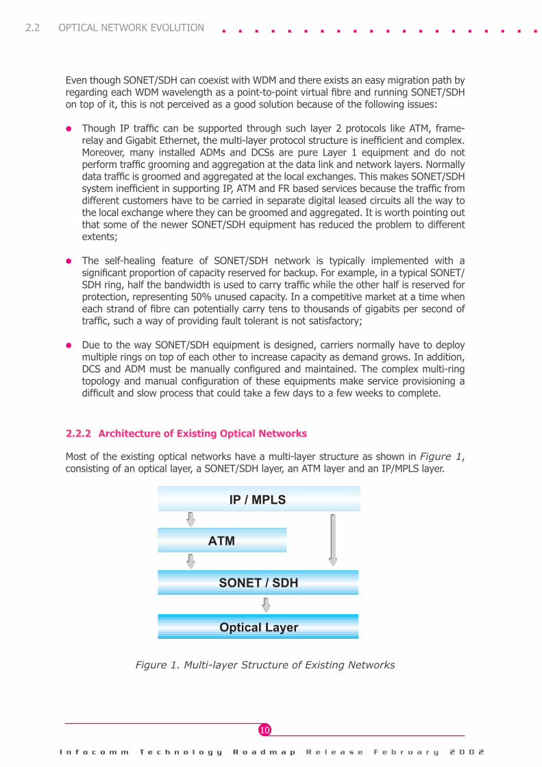
2.2.2 Architecture of Existing Optical Networks
Most of the existing optical networks have a multi-layer structure as shown in Figure 1, consisting of an optical layer, a SONET/SDH layer, an ATM layer and an IP/MPLS layer.
Figure 1. Multi-layer Structure of Existing Networks
2.2 OPTICAL NETWORK EVOLUTION
I n f o c o m m T e c h n o l o g y R o a d m a p R e l e a s e F e b r u a r y 2 0 0 2
11
NE
XT
GE
NE
RA
TIO
N O
PT
ICA
L NE
TW
OR
KS
In today’s networks, the optical layer is primarily dealing with signal transmission, amplication and reception. Switching and intelligence are done in the electronic realm. Therefore OEO conversion is required. In the case of a WDM system, it also includes static cross-connection of wavelengths and bres and static add-drop of wavelengths.
From the users’ perspectives, SONET/SDH equipment connects the bre cable plant and transmission facilities and converts them into a circuit-switched network, where xed bandwidth circuits of discrete data rates can be allocated and leased for different services and applications. Different types of networks such as an ATM network, a frame-relay network or an enterprise-wide area network can be overlaid on top of a SONET/SDH network using its xed bandwidth circuits at different bit rates. From a carrier’s perspective, SONET/SDH provides good fault-tolerant that ensures minimum disruption of services to the customers when there is a bre cut, network node failure and other types of failure. It eases operation, management and maintenance by providing a rich set of OAM functions. It is also able to meet the bandwidth requirements of different users and applications by providing a multiplexing hierarchy that supports a multitude of bit rates.
While the SONET/SDH can readily support telephony, ISDN and leased-line services, data and multimedia services and other advanced service offerings are best supported by an ATM network overlaying on the SONET/SDH network. The ATM network allows statistical multiplexing of trafc from different customers and different applications. ATM can provide trafc control and QoS assurance to individual trafc streams. Each trafc stream can be a particular type of trafc from a particular customer, a particular type of trafc from a closed user group, all the trafc from a particular site, or classied in some other way. The overlaying ATM network can also optimise trafc delivery for different service offerings by means of its own routing mechanisms. Because of its ability to support QoS, voice and other real-time trafc can be supported alongside data and other trafc via the ATM interface.
At present, there are two major approaches for a service provider to build an IP network that will route IP trafc and support IP/MPLS services; namely, IP over ATM over SONET/SDH and Packet over SONET/SDH, which are depicted in Figure 1. For the IP over ATM approach, IP trafc can be carried over the ATM network based on Classical Internet Protocol (CLIP) over ATM dened by RFC 1577 or Multiprotocol Encapsulation over AAL5 solution by RFC 1483. Alternatively, the MPLS solution dened by RFC 3031 can be used to carry IP trafc over an ATM network.
IP over ATM. The IP over ATM solution regards the underlying ATM network as pockets of ATM clouds (subnetworks) with each cloud connecting IP hosts and router interfaces belonging to the same IP subnet. The mapping between an IP address and the ATM address is provided by means of an Address Resolution Protocol (ARP) server, which could be a standalone server but it normally resides on an ATM equipment. There are several problems with this solution. Firstly, the IP layer has no inuence over how the IP trafc is routed in the underlying ATM network, so routing is generally not optimised. Secondly, the ATM layer simply regards each IP packet as an independent entity and provides only a connectionless oriented service. As such IP services and applications cannot take advantage of the QoS provisioning of ATM. Thirdly, scalability is a problem because a virtual connection needs to be provided between each IP router within the same IP subnet to establish a full-mesh logical connection and between each active IP host and router that have trafc exchanges. In addition, such a full-mesh could result in routing protocol trafc ooding the network when the network topology is not stable either due to network component failure or some form of dial-on-demand routing is used for certain link.
I n f o c o m m T e c h n o l o g y R o a d m a p R e l e a s e F e b r u a r y 2 0 0 2
12
Multiprotocol Label Switching (MPLS). MPLS is a new approach for deploying IP network that has been standardised by IETF over the last few years. It separates the routing and trafc control function from the packet forwarding function and provides a mechanism for information about network connectivity, bandwidth and utilisation that is available to a Layer 2 protocol, e.g., ATM or frame-relay, to be made known to Layer 3, i.e., IP layer. By doing so, it allows the control plane to be developed independently from the packet forwarding mechanism, and better routing and trafc engineering decisions to be made by making use of the information learned by the underlying Layer 2 protocol. In addition, its ability to partition and label IP packets belonging to the same ow allow differentiated QoS and service level agreements to be offered.
MPLS makes use of label switching for packet forwarding, much like ATM. An MPLS network consists of a number of Label Switching Routers (LSRs) interconnected in an arbitrary way. A small, xed-format label is attached to each packet at the ingress router. The label identi-es the packet as belonging to a particular forward equivalence class (FEC). A FEC is an MPLS terminology that refers to packets that share the same attributes and should be treated by the router in the same way. The concept of FEC allows different forwarding granularities to be used; for example, an FEC can be dened for packets that matches a particular IP address prex or dened for a particular pair of source and destination IP addresses and a particular application, e.g., real-video, http or telnet.
Among the advantages of MPLS is its ability to provide differentiated QoS to IP trafc ow and thus allow service level agreements to their customers and MPLS is generally viewed as a good way for trafc engineering and virtual private network provisioning. The packet is forwarded at each LSR by using the combination of incoming label value and interface to reference a lookup table to determine its next hop and the new label value it should take. The label is removed at the egress router where normal IP routing and forwarding will take place. This forwarding mechanism can be performed in hardware and is potentially much faster than the conventional longest IP address prex match approach used in a conven-tional IP router. It is essentially the same as how ATM and frame-relay cells are forwarded and, as such, an ATM or frame-relay switch can be turned into an LSR by adding an MPLS control module. The exact format of the label and how it is added to the packet depends on the Layer 2 technology. For ATM, the label is carried in the VCI and VPI elds of the ATM header; for frame-relay, it is carried in the DLCI eld; for such Layer 2 protocol like Ethernet and PPP, a MPLS shim header is inserted between the Layer 2 and Layer 3 header.
The control plane is responsible for maintaining the IP routing table and a label information base (LIB). The IP routing table can be maintained via a conventional interior gateway protocol such as Open Shortest Path First (OSPF). LIB can be maintained by the Label Distribution Protocol (LDP) specied in IETF RFC 3036 or other protocols.
Packet over SONET/SDH (POS). The IP/MPLS over ATM over SONET/SDH approach has a number of advantages in supporting data, voice and other services in a unied manner, and has been the only viable solution in the past for service providers and enterprises to set up a high-speed multiservice network. One of the key disadvantages of the ATM-centric approach is the high overhead added to a small cell size of 53 bytes. Depending on the average packet size, the ATM header and other overheads, such as the AAL Type 5 and IP packet headers, will result in 10 – 20% of wasted bandwidth for IP trafc. In addition, the original assumption that ATM would eventually be the solution from the backbone network all the way to the desktop has been quashed by the unchallenged dominant of Ethernet
2.2 OPTICAL NETWORK EVOLUTION
I n f o c o m m T e c h n o l o g y R o a d m a p R e l e a s e F e b r u a r y 2 0 0 2
13
NE
XT
GE
NE
RA
TIO
N O
PT
ICA
L NE
TW
OR
KS
in the LAN and enterprise network arena, making ATM less attractive to be used in the backbone. The above problems have motivated the POS solution to be developed. Certain framing and encapsulation method has been dened for POS. Thus far, the solution is based on the PPP over SONET/SDH specications dened in IETF RFC 2615. Though some vendors make use of Diffserv ore some proprietary solutions for providing differentiated QoS at the IP layer, it is still not clear how such an approach will fare in view of the growing importance of the MPLS approach, which seems to offer more exibility and is future-safe.
2.2.3 Architecture of Next Generation Optical Network, Issues and Challenges
Solutions such as POS, IP/MPLS over ATM over SONET/SDH, Multiservice Provisioning Platform (MSPP) etc, have actually helped to prolong the life span of the legacy SONET/SDH systems. It is clear that whatever form the next generation optical network will take, IP and DWDM will be featured prominently.
IP over WDM. The fact that the existing multi-layer architecture consisting of different protocol combinations of IP, ATM and SONET is inefcient and complex have quite naturally led to the notion of an IP over WDM architecture. However, what is meant by IP over WDM is subjected to different interpretation. The term IP over WDM, when interpreted narrowly, implies converting IP packets into optical signal directly and transmits onto a WDM transport network without any intermediate layer/protocol. However, this is not a practical proposition because not all the essential functions of these layers can be implemented at the IP layer or WDM layer. For example, encapsulation is required to get an IP packet onto a wavelength, so that the start and end of each IP packet can be recognised and that bit boundary is clearly identied. Due to lack of commercially available optical signal processing and framing solutions, this function still needs to be provided electronically at the point where IP packets are to be converted into electronic signals for processing and routing.
On the other hand, if IP over WDM is interpreted in the broad sense, it can refer to any architecture that has an IP layer, a WDM layer with any protocol layers in between the two, including many protocol architectures that are in use today. Here, we interpret IP over WDM in the broad sense but bearing in mind that it is evolving towards a streamlined structure with most of the functionalities essential for implementing large-scale optical networks being shifted to the IP layer or the optical/WDM layer.
At present, there are two major developments that are expected to have signicant impact on the eventual form of an IP over WDM network. The rst is the development of an all-encompassing and exible framing scheme, called digital wrapper, that will provide SONET/SDH like management features while allowing a wide variety of protocols and trafc to be supported almost directly on top of the optical layer. The next is the development of an optical control plane that will control Layer 1 to Layer 3 equipment in a unied manner and has the exibility for carriers and service providers to implement their networks to suit their individual requirements using different combinations of existing and new data forwarding technologies. These two developments are discussed below.
I n f o c o m m T e c h n o l o g y R o a d m a p R e l e a s e F e b r u a r y 2 0 0 2
14
Use of Digital Wrappers. There is much hope that future optical networks will eventually be all-optical, consisting of all-optical wavelength routers, add-drop multiplexers, wavelength converters, and optical 3R regeneration (re-amplication, re-shape and re-time) that will provide end-to-end wavelength services in a large scale network that spans large geographical distance and supports a large number of simultaneous wavelengths. Small-scale all-optical networks without optical 3R and wavelength conversions can be implemented with all-optical crossconnect switches and add/drop multiplexers that are readily available. However, large-scale all-optical networks that require wavelength conversions to provide the exibility and scalability, and optical 3R to eliminate impairment accumulation will not be commercially viable in the near future.
In the near term, it is more realistic to expect that some kind of OEO conversions will still be required in large-scale optical networks, perhaps with pockets of small, optically transparent subnetworks connected with equipment that will provide 3R regeneration and other functionalities in the electronic domain. This notion of a next generation optical network has motivated the development of “Digital Wrapper”, which can be seen as an equivalence of SONET/SDH in the relatively simple rst generation optical transport network based on single-wavelength transmission. It has been standardised by ITU-T in Recommendation G.709.
Digital Wrapper has a frame structure similar to SONET/SDH, which has overhead bits in the frame header to allow each wavelength to be managed as a discrete optical channel (OCh). It is able to provide optical-layer performance monitoring, and network protection on a per-channel basis, independent of the input signal format. In addition, it makes provision for an optional forward error correction (FEC) function to be supported with an additional overhead of 1024 bytes in the trailer. The FEC function serves to improve the bit error rate performance and, thus, enable the regenerator spacing to be extended by 100 to 300km at the expense of a slight increase in the overhead. By simply encapsulating or “wrapping” the signals without disrupting the bit-rate, format or timing of the signal, Digital Wrapper is able to carry a wide variety of client signals that include SONET/SDH, IP, ATM, GbE and Simplied Data Link (SDL). One of the key advantages of Digital Wrapper is that its does not assume that IP will be the only protocol in use in next generation optical network and thus enable the protocol architecture to evolve gracefully.
Emerging Optical Control Plane. The trafc evolution is such that it makes economic sense for IP to be the convergence layer to support different types of services, including voice and possibly video, which have more stringent QoS requirements than the conventional ‘best effort’ service the IP layer provides. Thus far, the most promising way to support such an IP-centric architecture is by means of MPLS, which is described in the previous section.
The concept of using MPLS in a common control plane to control the packet forwarding equipment in the data plane can easily be extended to the next generation optical network, be it an optically transparent network or an optically translucent ones. Translucent means that some opto-electronic conversions are required in the network. Such an expansion in scope will require MPLS to be enhanced so that it will be able to control not only packet switching equipment such as IP routers and ATM switches but also SONET/SDH equipment such as DCS and ADM and WDM equipment such as Optical Crossconnect (OXC) and Optical add-drop multiplexer (OADM). There are three ways for Label Switching Routers (LSRs) in the optical transport network (OTN) and IP routers in the IP layer to interact; they are best known as peer model, overlay model and hybrid model. In the context of GMPLS,
2.2 OPTICAL NETWORK EVOLUTION
I n f o c o m m T e c h n o l o g y R o a d m a p R e l e a s e F e b r u a r y 2 0 0 2
15
NE
XT
GE
NE
RA
TIO
N O
PT
ICA
L NE
TW
OR
KS
LSRs are GMPLS enabled network equipment in the OTN; e.g., OXC, OADM, SONET/SDH DCS or ADM.
The peer model has a single routing domain for all IP routers and optical transport network equipment. What it means is that the IP routers are aware of the topology, bandwidth and other connectivity information within the OTN and are able to inuence the routing decisions within the OTN to optimise network performance. Though the transparency can help to optimise routing and network performance, a peer model is only applicable if all the IP routers and OTN equipment belong to the same administrative domain.
In the overlay model, the OTN appears as an optical cloud or black box whose internal structure is not visible to the IP routers and other types of devices that it connects to. These IP routers and devices are the clients of the OTN and can initiate connectivity requests through an Optical User-to-Network (O_UNI) interface. Since the client layer and the OTN have their own routing domains and make independent routing decisions, the resulting network is more complex and routing is not optimal. This model is applicable where the service providers and corporate clients only lease wavelengths or TDM circuits from carriers.
The hybrid model is simply a combination of the peer model and the overlay model. This model is applicable where a carrier’s network consists of LSRs and IP routers and provides both wavelength and IP services to the client. The hybrid model offers substantial exibility to carriers and service providers to deploy the most cost-effective model for their needs. In order to support these models, the signaling and routing protocols of GMPLS need to be enhanced. In addition, unlike in the electronic domain where label could be inserted, removed and processed easily, there is no practical way to generate a physical optical label that can be inserted, dropped, optically processed and based on it to route optical packets.
There is a proposal based on the use of an abstract label that is explicitly dened by virtual of the position of the packet within the hierarchical structure of bre bundle, bre, wavelength, and time slot within a TDM frame (assuming that SONET/SDH or other TDM equipment is used to provide fractional wavelength service). Further work is required to address the scalability of the above approach or to devise a new approach because the MPLS label space is in the order of one million per port while the number of wavelengths and TDM channels are in the order of tens to hundreds per port.
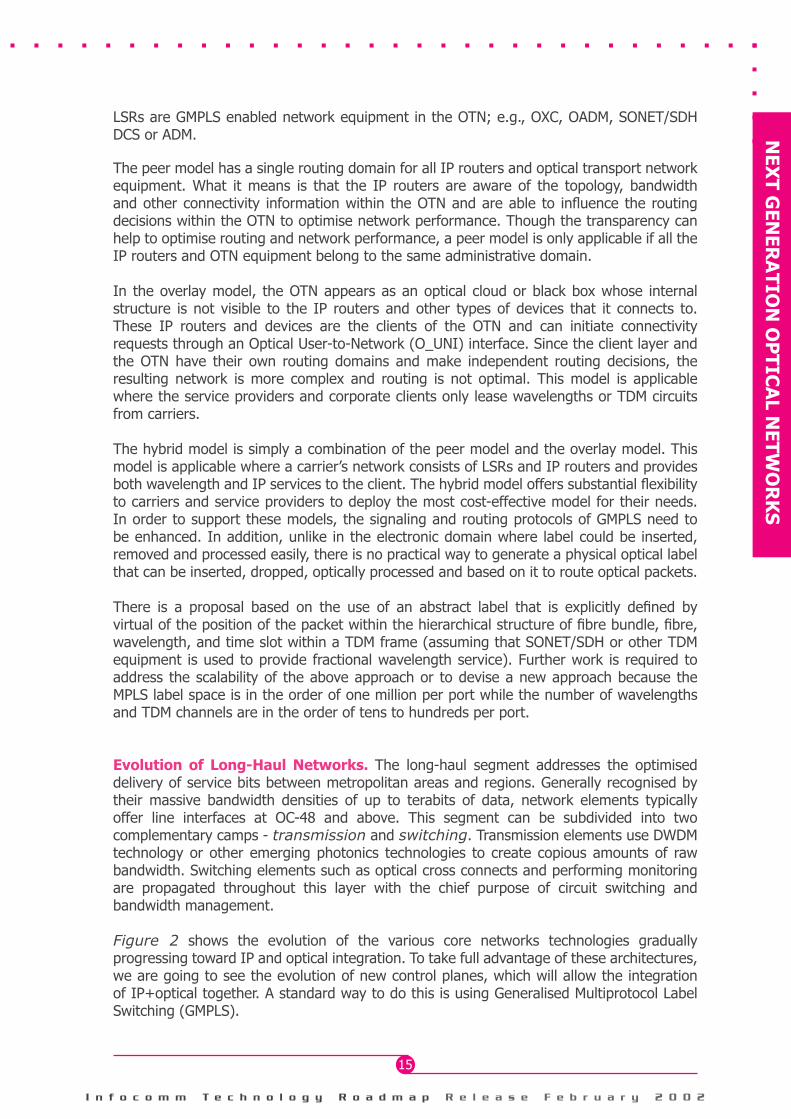
Evolution of Long-Haul Networks. The long-haul segment addresses the optimised delivery of service bits between metropolitan areas and regions. Generally recognised by their massive bandwidth densities of up to terabits of data, network elements typically offer line interfaces at OC-48 and above. This segment can be subdivided into two complementary camps - transmission and switching. Transmission elements use DWDM technology or other emerging photonics technologies to create copious amounts of raw bandwidth. Switching elements such as optical cross connects and performing monitoring are propagated throughout this layer with the chief purpose of circuit switching and bandwidth management.
Figure 2 shows the evolution of the various core networks technologies gradually progressing toward IP and optical integration. To take full advantage of these architectures, we are going to see the evolution of new control planes, which will allow the integration of IP+optical together. A standard way to do this is using Generalised Multiprotocol Label Switching (GMPLS).
I n f o c o m m T e c h n o l o g y R o a d m a p R e l e a s e F e b r u a r y 2 0 0 2
16
Figure 2. Evolution of Optical Networks in Long-Haul
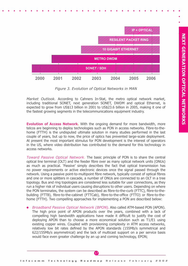
Evolution of Metropolitan Network. Metropolitan transport functionality deals princi-pally with the task of bandwidth management and grooming for the efcient transport of services among multiple Points of Presences (POPs) or Central Ofces in a particular geo-graphical area. Typical network elements that offer solutions in this segment have band-width density of up to few hundreds gigabits-per-second, and offer line support up to OC-48 (with OC-192 on the horizon).
Many architectures and solutions are currently being proposed for next-generation met-ropolitan area network architectures. This is depicted in Figure 3. What we will see in this segment will be a multi-directional development of existing technology such as SONET/SDH, coexisting with newer technologies such as metro DWDM, and 10GbE and RPR in the near future.
As bandwidth demand increases, SONET would be progressively displaced. In its place, we will see services provisioned directly over the optical layer eventually. The SONET/SDH has started to evolve toward systems with multi service optimisation. These data-optimised SONET/SDH access optical transport systems, also known as Multiservice Provisioning Platforms (MSPPs), offer consolidated multi services capability coupled with traditional transport technologies such as DWDM and/or SONET. MSPPs offer the combined benet of transport plus layer two or three data intelligence for MAN.
In the near term, emerging technologies such as 10GbE and Resilient Packet Ring (RPR) are envisaged to position strongly in this segment of the network. This would mean that pre-standard product will start to enter this market.
The end goal is to unify IP+optical together to deliver services even more efciently. IP+optical means effectively the integration of IP and optical, which is a method of controlling the optical plane by an IP-derived intelligence, or integrating IP routing and trafc engineering with the optical layer.
2.2 OPTICAL NETWORK EVOLUTION
I n f o c o m m T e c h n o l o g y R o a d m a p R e l e a s e F e b r u a r y 2 0 0 2
17
NE
XT
GE
NE
RA
TIO
N O
PT
ICA
L NE
TW
OR
KS
IP + OPTICAL
RESILENT PACKET RING
METRO DWDM
10 GIGABIT ETHERNET
SONET / SDH
2000 2001 2002 2003 2004 2005 2006
Figure 3. Evolution of Optical Networks in MAN
Market Outlook. According to Cahners In-Stat, the metro optical network market, including traditional SONET, next generation SONET, DWDM and optical Ethernet, is expected to grow from US$13 billion in 2001 to US$23.6 billion in 2005, making it one of the fastest growing segments in the telecommunications equipment industry.
Evolution of Access Network. With the ongoing demand for more bandwidth, more telcos are beginning to deploy technologies such as PON in access networks. Fibre-to-the-home (FTTH) is the undisputed ultimate solution in many studies performed in the last couple of years, but up to now, the price of optics has prevented large-scale deployment. At present the most important stimulus for PON development is the interest of operators in the US, where video distribution has contributed to the demand for this technology in access networks.
Toward Passive Optical Network. The basic principle of PON is to share the central optical line terminal (OLT) and the feeder bre over as many optical network units (ONUs) as much as practical. ‘Passive’ simply describes the fact that optical transmission has no power requirements or active electronic devices once the signal passed through the network. Using a passive point-to-multipoint bre network, typically consist of optical bres and one or more splitters in cascade, a number of ONUs are connected to an OLT in a tree topology. Bus and ring topologies are considered less suitable for user connections, as they run a higher risk of individual users causing disruptions to other users. Depending on where the PON terminates, the system can be described as bre-to-the-curb (FTTC), bre-to-the-building (FTTB), bre-to-the-cabinet (FTTCab), bre-to-the-ofce (FTTO) or bre-to-the-home (FTTH). Two compelling approaches for implementing a PON are described below:
Broadband Passive Optical Network (BPON). Also called ATM-based PON (APON). The high price point of APON products over the years, combined with a lack of compelling high bandwidth applications have made it difcult to justify the cost of deploying APON than to choose a more economical solution such as T1/E1 using existing copper wires. Coupled with provisioning complexity in ATM access networks, relatively low bit rates dened by the APON standards (155Mb/s symmetrical and 622/155Mb/s asymmetrical) and the lack of multicast support on a per service basis would face even greater challenge by an up and coming technology, EPON;
I n f o c o m m T e c h n o l o g y R o a d m a p R e l e a s e F e b r u a r y 2 0 0 2
18
Ethernet Passive Optical Network (EPON). EPON evolution is driven by the fact that most of the data trafc within enterprises and outwards to the network is IP/Ethernet based. Ethernet is highly suitable for transporting IP data considering that the variable length structure of the Ethernet frame has a much larger maximum size of 1518 bytes. One of its attractiveness is the large price difference between Ethernet components and ATM components. The former has a much larger market due to its dominant in the enterprise network market. However, EPON technology is still not fully dened. It lacks two major functionalities. One is the OAM&P functionality, which is well dened in APON systems but not well established in Ethernet systems. This feature is important for operators to carry out network monitoring. Another important functionality that is lacking is QoS provisioning. Although data networks utilising Ethernet have various mechanisms to provide QOS i.e. priority schemes (802.1p) and diffserve for delay/latency/jitter sensitive applications such as voice and multimedia, they inherently add complexity and cost to the network due to the sophisticated protocols, and complicated management and provisioning issues.
2.3 STANDARD DEVELOPMENTS
In this section, we will cover the most important standardisation activities currently in development by the various standard bodies such as ITU, IETF, IEEE, and industry organisations such as OIF, RPR and 10Gigabit Ethernet alliance.
2.3.1 ITU-T
The standardisation work related to Optical Networks is carried out in two Study Groups within ITU-T:
Study Group 15 is the lead Study Group and it undertakes areas related to optical and other transport networks. It is responsible for most G-series standards except for those assigned to Study Group 2, 4, 13 and 16;
Study Group 13 covers Multi-protocol and IP-based networks and their internetworking areas. It is responsible for the G.900 series and some I-series standards.
Current to the date of writing, ITU-T has approved a number of important recommendations in optical networking (see Table 1). The recommendations in boldface are the new Optical Network recommendations complementing the existing one used in transmission networks.
2.3 STANDARD DEVELOPMENTS
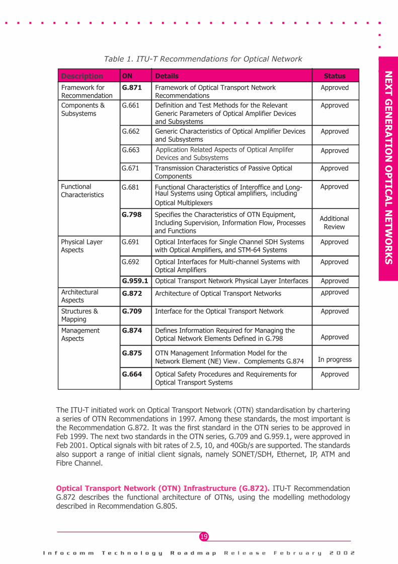
I n f o c o m m T e c h n o l o g y R o a d m a p R e l e a s e F e b r u a r y 2 0 0 2
19
NE
XT
GE
NE
RA
TIO
N O
PT
ICA
L NE
TW
OR
KS
Table 1. ITU-T Recommendations for Optical Network
The ITU-T initiated work on Optical Transport Network (OTN) standardisation by chartering a series of OTN Recommendations in 1997. Among these standards, the most important is the Recommendation G.872. It was the rst standard in the OTN series to be approved in Feb 1999. The next two standards in the OTN series, G.709 and G.959.1, were approved in Feb 2001. Optical signals with bit rates of 2.5, 10, and 40Gb/s are supported. The standards also support a range of initial client signals, namely SONET/SDH, Ethernet, IP, ATM and Fibre Channel.
Optical Transport Network (OTN) Infrastructure (G.872). ITU-T Recommendation G.872 describes the functional architecture of OTNs, using the modelling methodology described in Recommendation G.805.
Haul Systems using Optical amplifiers, Including
Description ON Details Status
Framework forRecommendation
G.871 Framework of Optical Transport NetworkRecommendations
Approved
G.661 Definition and Test Methods for the RelevantGeneric Parameters of Optical Amplifier Devicesand Subsystems
Approved
G.662 Generic Characteristics of Optical Amplifier Devicesand Subsystems
Approved
G.663 Approved
Components &Subsystems
Description
G.671 Transmission Characteristics of Passive OpticalComponents
Approved
G.681 Functional Characteristics of Interoffice and Long-
Optical Multiplexers
ApprovedFunctionalCharacteristics
G.798 Specifies the Characteristics of OTN Equipment,Including Supervision, Information Flow, Processesand Functions
AdditionalReview
G.691 Optical Interfaces for Single Channel SDH Systemswith Optical Amplifiers, and STM-64 Systems
ApprovedPhysical LayerAspects
G.692 Optical Interfaces for Multi-channel Systems withOptical Amplifiers
Approved
G.959.1 Optical Transport Network Physical Layer Interfaces Approved
ArchitecturalAspects
G.872 Architecture of Optical Transport Networks Approved
Structures &Mapping
G.709 Interface for the Optical Transport Network Approved
G.874 Defines Information Required for Managing theOptical Network Elements Defined in G.798 Approved
G.875 eIn progress
ManagementAspects
G.664 Optical Safety Procedures and Requirements forOptical Transport Systems
Approved
Application Related Aspects of Optical AmpliferDevices and Subsystems
i
“OTN Management Information Model for thNetwork Element (NE) View”. Complements G.874.

I n f o c o m m T e c h n o l o g y R o a d m a p R e l e a s e F e b r u a r y 2 0 0 2
20
The architecture denes a layered structure with three distinct layers, as shown in Figure 4.
Optical Channel layer network (OCh). This layer provides for an end-to-end transport of client signals (e.g. SONET/SDH, ATM cells) through an optical trail between access points. Functions in this layer include:
§ Connection re-arrangement for exible network routing;
§ Overhead functions for ensuring integrity of the optical channel adapted information;
§ Supervisory functions for enabling network level operations and management functions, such as connection provisioning, quality of service parameter exchange and network survivability.
Optical Multiplex Section layer network (OMS). This layer provides the functionality required for the proper operation of a multi-wavelength transmission system. This includes:
§ Overhead functions for ensuring integrity of the multi-wavelength multiplex section adapted information;
§ Supervisory functions for enabling section level operations and management functions, such as multiplex section survivability.
Optical Transmission Section layer network (OTS). This is the lowest layer and deals with transmission of optical signals on various types of optical bre media (e.g. G.652, G.653 and G.655 bre). It also has its own overhead and supervisory functions for ensuring proper operation at its level.
Optical Channel(OCh)
Optical Transmission Section(OTSn)
Optical Multiplex Section(OMSn)
IP ATM Ethernet STM-n
Figure 4. Layered Structure of OTN
Adaptations take place in between adjacent layers. The adaptation of client signal to the OCh layer involves generating a continuous data stream for subsequent modulation. The OCh/OMS adaptation allocates wavelength to each OCh and modulates the channel’s data stream onto the allocated optical carrier or wavelength. All channels are multiplexed together and handed over to the OTS layer. The OMS/OTS adaptation handles the management and monitoring function necessary for the OMS.
As shown in Figure 5, multiple OChs are optically multiplexed together to create an OMS to be carried over a DWDM system. Each of these optical channels consists of client signals mapped from its digital format. The OMS is transported optically over a span of optical bre that constitutes the OTS.
2.3 STANDARD DEVELOPMENTS
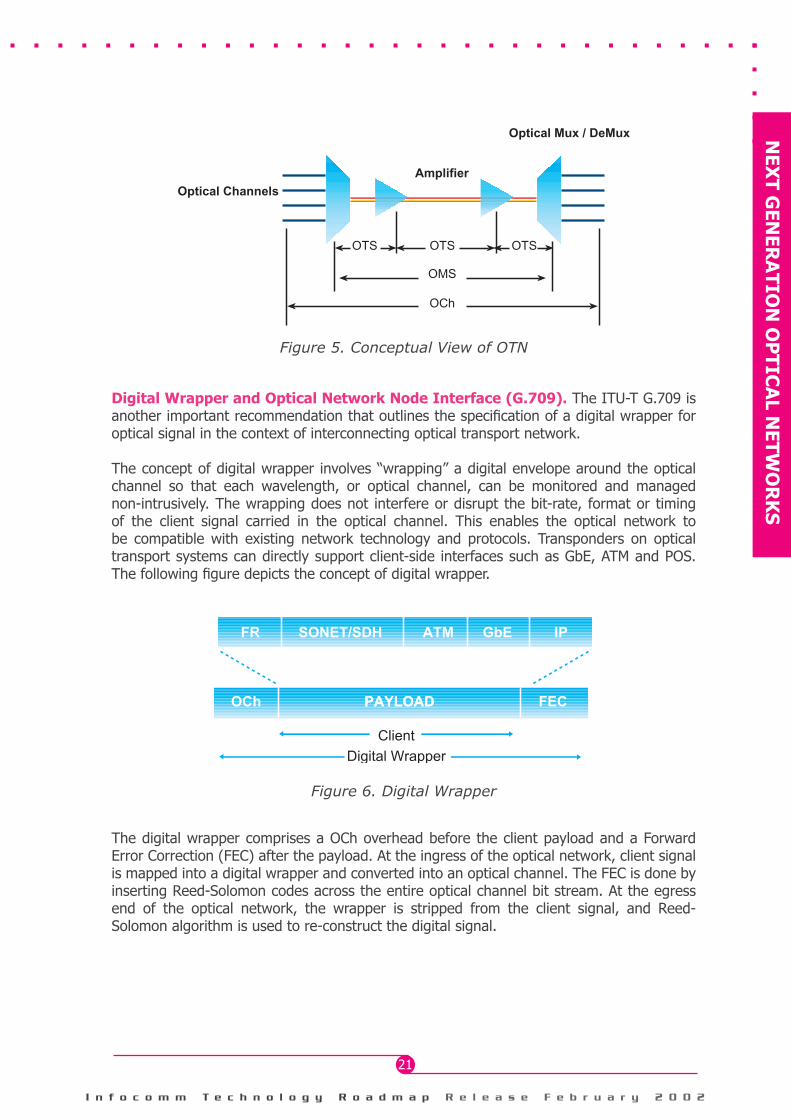
I n f o c o m m T e c h n o l o g y R o a d m a p R e l e a s e F e b r u a r y 2 0 0 2
21
NE
XT
GE
NE
RA
TIO
N O
PT
ICA
L NE
TW
OR
KS
AmplifierOptical Channels
Optical Mux / DeMux
OCh
OMS
OTSOTS OTS
Figure 5. Conceptual View of OTN
Digital Wrapper and Optical Network Node Interface (G.709). The ITU-T G.709 is another important recommendation that outlines the specication of a digital wrapper for optical signal in the context of interconnecting optical transport network.
The concept of digital wrapper involves “wrapping” a digital envelope around the optical channel so that each wavelength, or optical channel, can be monitored and managed non-intrusively. The wrapping does not interfere or disrupt the bit-rate, format or timing of the client signal carried in the optical channel. This enables the optical network to be compatible with existing network technology and protocols. Transponders on optical transport systems can directly support client-side interfaces such as GbE, ATM and POS. The following gure depicts the concept of digital wrapper.
Figure 6. Digital Wrapper
The digital wrapper comprises a OCh overhead before the client payload and a Forward Error Correction (FEC) after the payload. At the ingress of the optical network, client signal is mapped into a digital wrapper and converted into an optical channel. The FEC is done by inserting Reed-Solomon codes across the entire optical channel bit stream. At the egress end of the optical network, the wrapper is stripped from the client signal, and Reed-Solomon algorithm is used to re-construct the digital signal.
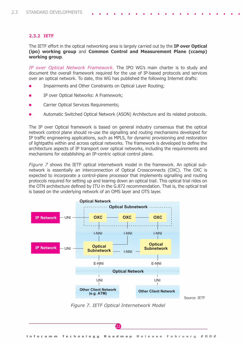
I n f o c o m m T e c h n o l o g y R o a d m a p R e l e a s e F e b r u a r y 2 0 0 2
22
2.3.2 IETF
The IETF effort in the optical networking area is largely carried out by the IP over Optical (ipo) working group and Common Control and Measurement Plane (ccamp) working group.
IP over Optical Network Framework. The IPO WG’s main charter is to study and document the overall framework required for the use of IP-based protocols and services over an optical network. To date, this WG has published the following Internet drafts:
Impairments and Other Constraints on Optical Layer Routing;
IP over Optical Networks: A Framework;
Carrier Optical Services Requirements;
Automatic Switched Optical Network (ASON) Architecture and its related protocols.
The IP over Optical framework is based on general industry consensus that the optical network control plane should re-use the signalling and routing mechanisms developed for IP trafc engineering applications, such as MPLS, for dynamic provisioning and restoration of lightpaths within and across optical networks. The framework is developed to dene the architecture aspects of IP transport over optical networks, including the requirements and mechanisms for establishing an IP-centric optical control plane.
Figure 7 shows the IETF optical internetwork model in the framework. An optical sub-network is essentially an interconnection of Optical Crossconnects (OXC). The OXC is expected to incorporate a control-plane processor that implements signalling and routing protocols required for setting up and tearing down an optical trail. This optical trial rides on the OTN architecture dened by ITU in the G.872 recommendation. That is, the optical trail is based on the underlying network of an OMS layer and OTS layer.
Source: IETF
Figure 7. IETF Optical Internetwork Model
2.3 STANDARD DEVELOPMENTS
I n f o c o m m T e c h n o l o g y R o a d m a p R e l e a s e F e b r u a r y 2 0 0 2
23
NE
XT
GE
NE
RA
TIO
N O
PT
ICA
L NE
TW
OR
KS
Client networks such as ATM or SONET/SDH connects to an optical core network via an IP router over a User-Network Interface (UNI). This is the service boundary where a service request for a connection is issued to the server, in this case, the optical network.
An optical network is an interconnection of optical sub-networks. Sub-networks within the same administrative domain are linked by Internal Node-to-Node Interface (INNI), where as optical network belong to different administrative domains are linked by External NNI (ENNI). The main difference between the INNI and ENNI lies in the policies that restrict information and control ow at the interface. In the case of ENNI, as the interconnected network belongs to different administrative domains, hiding of topological and security information is necessary.
IETF species two Interconnection models between the edge IP network and the optical core network, namely, the Peer Model and the Overlay Model.
In the Peer Model, the IP and optical networks are treated as a single integrated network from a control plane point of view. That is, the IP routers at the edge network and the OXCs in the optical network are treated like peers as far as control plane is concerned. There is no difference between UNI and NNI. This control plane is assumed to be MPLS-based. The IP and optical layers are assumed to run the same instance of an IP routing protocol (such as OSPF with optical extension). There is dynamic discovery of IP endpoints attached to the optical network. This enables a router to compute an end-to-end path to another router across the optical network. This model calls for IP router to have greater knowledge of topology and routing information of the optical network, as well as a higher level of control in determining the specic paths for connection across the optical network.
In the Overlay Model, there are two distinct network entities: the client network and the optical network that plays the role of a server, offering dynamic connection at the request of a client. This is done over the UNI. UNI signalling typically involves service requests such as light path creation, deletion, modication and status enquiry. Under this model, the IP/MPLS routing, topology distribution and signalling protocols are independent of the routing, topology distribution and signalling protocols at the optical layer. There is no routing exchange between the IP and optical domains.
In term of implementation complexity, the Overlay model is less complex than the Peer model, though each model has its own advantages. The current IETF framework draft recommends the evolution path that starts with simpler functionality in the beginning and includes more complex functionality later. Initial deployment is expected to be based on Overlay model. The next phase of evolution would introduce reachability information exchange between the IP and optical domains. This would enable optical trail to be established as part of the end-to-end LSP set-ups. The vision of IETF is the full Peer model where more sophisticated routing interaction take place between the IP and optical domains.
This evolution is made possible with the use of a common signalling framework based on GMPLS. The UNI Signalling Specication 1.0 developed by the Optical Internetworking Forum (OIF) is based on GMPLS. Although IETF GMPLS standards development is still in progress, the current version of OIF focus on functions required for near term deployment while having the long-term goal of continued alignment with GMPLS development. Overlay model based on this UNI specication would be able to evolve with richer functionality set as work in the Peer model become more sophisticated. There is no need for a complete re-development of signalling capabilities.
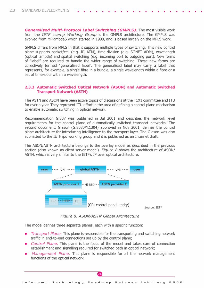
I n f o c o m m T e c h n o l o g y R o a d m a p R e l e a s e F e b r u a r y 2 0 0 2
24
Generalised Multi-Protocol Label Switching (GMPLS). The most visible work from the IETF ccamp Working Group is the GMPLS architecture. The GMPLS was evolved from MPlambdaS which started in 1999, and is based largely on the MPLS work.
GMPLS differs from MPLS in that it supports multiple types of switching. This new control plane supports packet/cell (e.g. IP, ATM), time-division (e.g. SONET ADM), wavelength (optical lambda) and spatial switching (e.g. incoming port to outgoing port). New forms of “label” are required to handle the wider range of switching. These new forms are collectively termed “generalised label”. The generalised label may carry a label that represents, for example, a single bre in a bundle, a single wavelength within a bre or a set of time-slots within a wavelength.
2.3.3 Automatic Switched Optical Network (ASON) and Automatic Switched Transport Network (ASTN)
The ASTN and ASON have been active topics of discussions at the T1X1 committee and ITU for over a year. They represent ITU effort in the area of dening a control plane mechanism to enable automatic switching in optical network.
Recommendation G.807 was published in Jul 2001 and describes the network level requirements for the control plane of automatically switched transport networks. The second document, G.ason (G.8080/Y.1304) approved in Nov 2001, denes the control plane architecture for introducing intelligence to the transport layer. The G.ason was also submitted to the IETF ipo working group and it is published as an Internet draft.
The ASON/ASTN architecture belongs to the overlay model as described in the previous section (also known as client-server model). Figure 8 shows the architecture of ASON/ASTN, which is very similar to the IETF’s IP over optical architecture.
(CP: control panel entity)Source: IETF
Figure 8. ASON/ASTN Global Architecture
The model denes three separate planes, each with a specic function:
Transport Plane. This plane is responsible for the transporting and switching network trafc in end-to-end connections set up by the control plane;
Control Plane. This plane is the focus of the model and takes care of connection establishment and signalling required for switched path in optical network;
Management Plane. This plane is responsible for all the network management functions of the optical network.
2.3 STANDARD DEVELOPMENTS
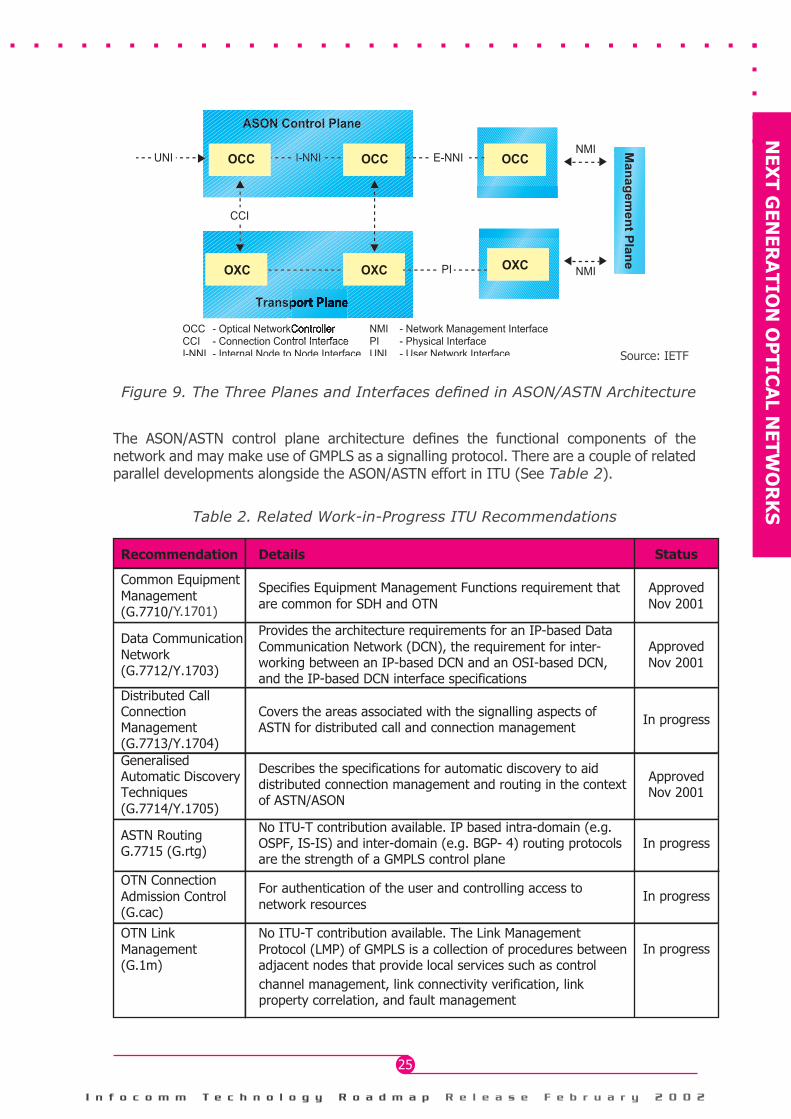
I n f o c o m m T e c h n o l o g y R o a d m a p R e l e a s e F e b r u a r y 2 0 0 2
25
NE
XT
GE
NE
RA
TIO
N O
PT
ICA
L NE
TW
OR
KS
Figure 9. The Three Planes and Interfaces dened in ASON/ASTN Architecture
The ASON/ASTN control plane architecture denes the functional components of the network and may make use of GMPLS as a signalling protocol. There are a couple of related parallel developments alongside the ASON/ASTN effort in ITU (See Table 2).
Table 2. Related Work-in-Progress ITU Recommendations
Source: IETF
Recommendation Details Status
Common EquipmentManagement(G.7710/Y1701)
Specifies Equipment Management Functions requirement thatare common for SDH and OTN
ApprovedNov 2001
Data CommunicationNetwork(G.7712/Y.1703)
Provides the architecture requirements for an IP-based DataCommunication Network (DCN), the requirement for inter-working between an IP-based DCN and an OSI-based DCN,and the IP-based DCN interface specifications
ApprovedNov 2001
Distributed CallConnectionManagement(G.7713/Y.1704)
Covers the areas associated with the signalling aspects ofASTN for distributed call and connection management In progress
GeneralisedAutomatic DiscoveryTechniques(G.7714/Y.1705)
Describes the specifications for automatic discovery to aiddistributed connection management and routing in the contextof ASTN/ASON
ApprovedNov 2001
ASTN RoutingG.7715 (G.rtg)
No ITU-T contribution available. IP based intra-domain (e.g.OSPF, IS-IS) and inter-domain (e.g. BGP- 4) routing protocolsare the strength of a GMPLS control plane
In progress
OTN ConnectionAdmission Control(G.cac)
For authentication of the user and controlling access tonetwork resources
In progress
OTN LinkManagement(G.1m)
No ITU-T contribution available. The Link ManagementProtocol (LMP) of GMPLS is a collection of procedures betweenadjacent nodes that provide local services such as control
In progress
channel management, link connectivity verification, linkproperty correlation, and fault management
Y.1701)
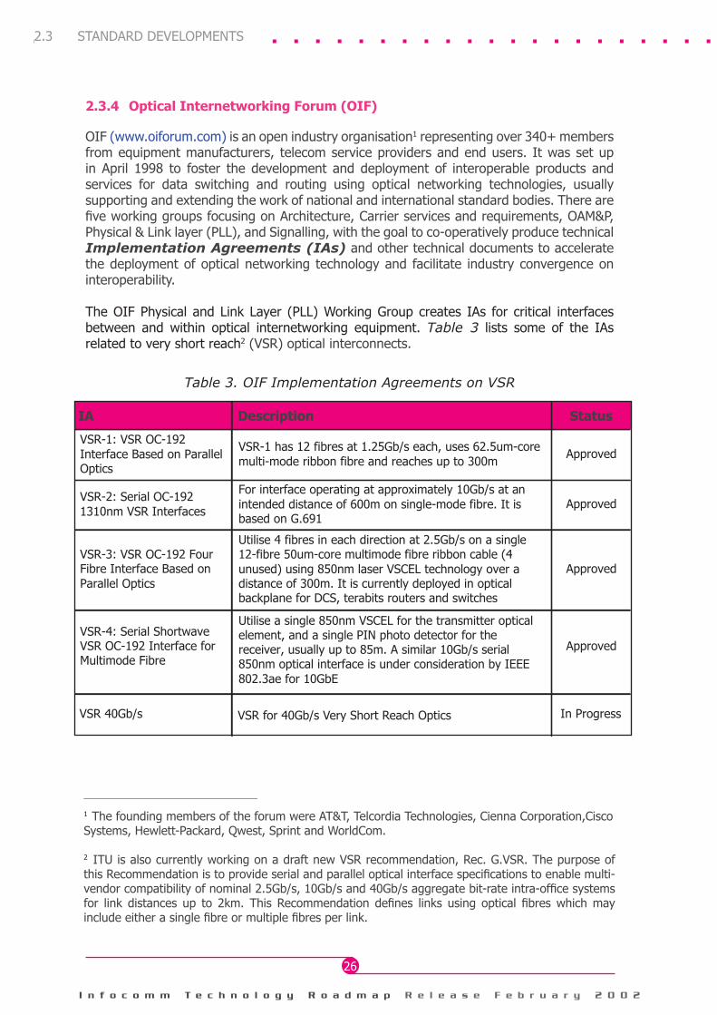
I n f o c o m m T e c h n o l o g y R o a d m a p R e l e a s e F e b r u a r y 2 0 0 2
26
2.3.4 Optical Internetworking Forum (OIF)
OIF (www.oiforum.com) is an open industry organisation1 representing over 340+ members from equipment manufacturers, telecom service providers and end users. It was set up in April 1998 to foster the development and deployment of interoperable products and services for data switching and routing using optical networking technologies, usually supporting and extending the work of national and international standard bodies. There are ve working groups focusing on Architecture, Carrier services and requirements, OAM&P, Physical & Link layer (PLL), and Signalling, with the goal to co-operatively produce technical Implementation Agreements (IAs) and other technical documents to accelerate the deployment of optical networking technology and facilitate industry convergence on interoperability.
The OIF Physical and Link Layer (PLL) Working Group creates IAs for critical interfaces between and within optical internetworking equipment. Table 3 lists some of the IAs related to very short reach2 (VSR) optical interconnects.
Table 3. OIF Implementation Agreements on VSR
2.3 STANDARD DEVELOPMENTS
1 The founding members of the forum were AT&T, Telcordia Technologies, Cienna Corporation,Cisco Systems, Hewlett-Packard, Qwest, Sprint and WorldCom.
2 ITU is also currently working on a draft new VSR recommendation, Rec. G.VSR. The purpose of this Recommendation is to provide serial and parallel optical interface specications to enable multi-vendor compatibility of nominal 2.5Gb/s, 10Gb/s and 40Gb/s aggregate bit-rate intra-ofce systems for link distances up to 2km. This Recommendation denes links using optical bres which may include either a single bre or multiple bres per link.
TA Description Status
VSR-1: VSR OC-192Interface Based on ParallelOptics
VSR-1 has 12 fibres at 1.25Gb/s each, uses 62.5um-coremulti-mode ribbon fibre and reaches up to 300m
Approved
VSR-2: Serial OC-1921310nm VSR Interfaces
For interface operating at approximately 10Gb/s at anintended distance of 600m on single-mode fibre. It isbased on G.691
Approved
VSR-3: VSR OC-192 FourFibre Interface Based onParallel Optics
Utilise 4 fibres in each direction at 2.5Gb/s on a single12-fibre 50um-core multimode fibre ribbon cable (4unused) using 850nm laser VSCEL technology over adistance of 300m. It is currently deployed in opticalbackplane for DCS, terabits routers and switches
Approved
VSR-4: Serial ShortwaveVSR OC-192 Interface forMultimode Fibre
Utilise a single 850nm VSCEL for the transmitter opticalelement, and a single PIN photo detector for thereceiver, usually up to 85m. A similar 10Gb/s serial850nm optical interface is under consideration by IEEE802.3ae for 10GbE
Approved
VSR 40Gb/s In ProgressVSR for 40Gb/s Very Short Reach Optics
IA Description Status
I n f o c o m m T e c h n o l o g y R o a d m a p R e l e a s e F e b r u a r y 2 0 0 2
27
NE
XT
GE
NE
RA
TIO
N O
PT
ICA
L NE
TW
OR
KS
Within the OIF, activities have been focused on establishing UNI signalling specications based on modications to the Resource Reservation Protocol with Trafc Engineering (RSVP-TE) and Constraint-routed Label Distribution Protocol (CR-LDP) protocols, for implementation as part of multi-vendor interoperability demonstrations.
OIF’s UNI 1.0 specication was completed in Oct 2001. The specication denes the signalling protocols implemented by client and transport network equipment from different vendors to invoke services, the mechanisms used to transport signalling messages and the auto-discovery procedure that aid signalling. The primary service that is offered by the transport network over the UNI is the ability to create and delete connections on-demand. As a next step to accelerate the deployment of interoperable, cost-effective and robust optical internetworks, the OIF is initiating effort to develop signalling specications for a network-to-network interface (NNI). Going forward, OIF UNI 2.0 will be developed to address a number of areas including security, bandwidth modication, extension to physical layer such as Ethernet and the ability to establish multiple connections with a single call.
2.3.5 Optical Domain Service Interconnect (ODSI)
The ODSI coalition is an informal industry forum formed in Jan 2000 to accelerate the practical evolution and use of the optical network through the development and promotion of an open interface between the electrical and optical layers. The coalition objective is to dene an optical UNI interface (O-UNI). This open interface is required to enable electrical layer devices such as IP routers and ATM switches to request high-speed optical channels on demand. The Coalition published the ODSI functional specication in end 2000. Its work was submitted for information purposes to ofcial standards-setting bodies. Today progress on the O-UNI continues in groups such as the OIF, ITU-T (G.ASON), and the IETF. With the submission of the specications, ODSI has came to a close.
2.3.6 IEEE Standard Development on Gigabit Ethernet & Resilient Packet Ring
IEEE 802.3 Working Group. The IEEE is currently working on two very important optical networking standards; 10 Gigabit Ethernet (802.3ae) and Resilient Packet Rings (802.17).
10 Gigabit Ethernet. With the development of Gigabit Ethernet some time ago, inexpensive interfaces with a transmission rate at 1Gb/s have been made available in most commercial products. Compared to the expensive ATM and Packet over SONET/SDH links, Gigabit Ethernet provides a cost-effective solution for deploying point-to-point gigabit connections. With the exponential growth of internet trafc, many service providers are seeing the need for 10Gb/s links.
As a consequence, the IEEE formed the P802.3ae 10Gb/s Ethernet Task Force (http://grouper.ieee.org/groups/802/3/ae/) in 1999 to develop a standard for 10-Gigabit Ethernet interface. The standard is planned for completion in Q1, 2002 (See Figure 10).
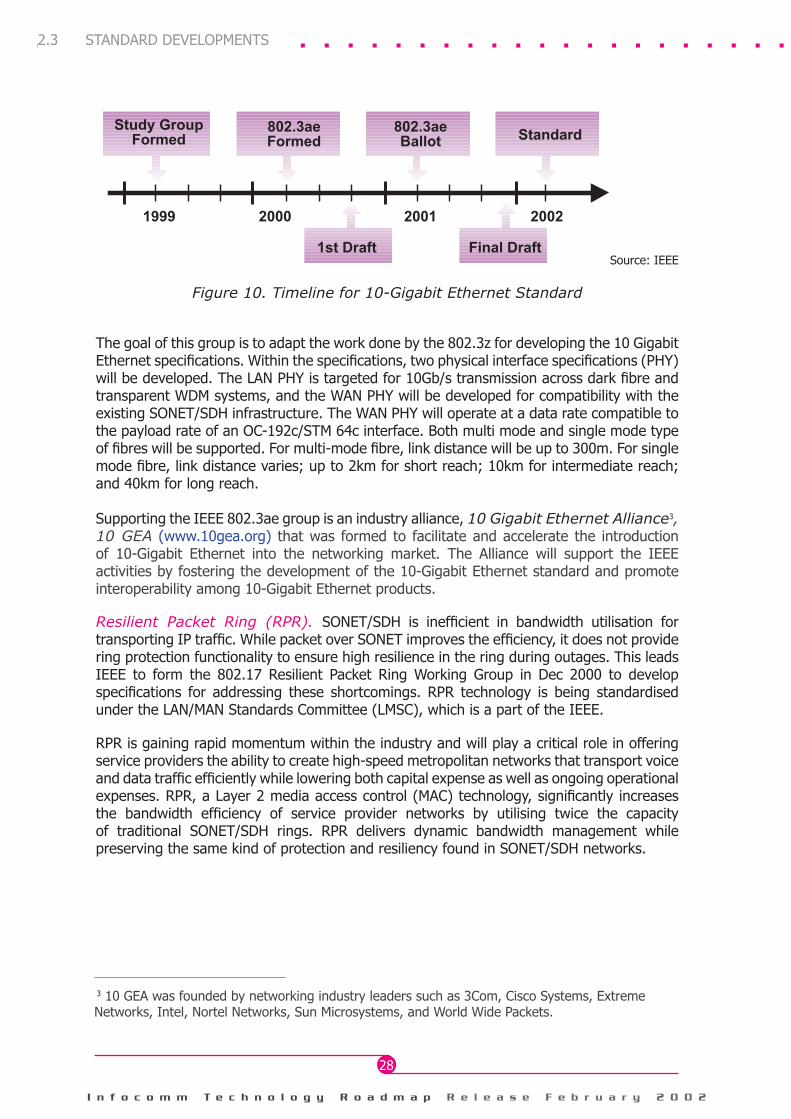
I n f o c o m m T e c h n o l o g y R o a d m a p R e l e a s e F e b r u a r y 2 0 0 2
28
Source: IEEE
Figure 10. Timeline for 10-Gigabit Ethernet Standard
The goal of this group is to adapt the work done by the 802.3z for developing the 10 Gigabit Ethernet specications. Within the specications, two physical interface specications (PHY) will be developed. The LAN PHY is targeted for 10Gb/s transmission across dark bre and transparent WDM systems, and the WAN PHY will be developed for compatibility with the existing SONET/SDH infrastructure. The WAN PHY will operate at a data rate compatible to the payload rate of an OC-192c/STM 64c interface. Both multi mode and single mode type of bres will be supported. For multi-mode bre, link distance will be up to 300m. For single mode bre, link distance varies; up to 2km for short reach; 10km for intermediate reach; and 40km for long reach.
Supporting the IEEE 802.3ae group is an industry alliance, 10 Gigabit Ethernet Alliance3, 10 GEA (www.10gea.org) that was formed to facilitate and accelerate the introduction of 10-Gigabit Ethernet into the networking market. The Alliance will support the IEEE activities by fostering the development of the 10-Gigabit Ethernet standard and promote interoperability among 10-Gigabit Ethernet products.
Resilient Packet Ring (RPR). SONET/SDH is inefcient in bandwidth utilisation for transporting IP trafc. While packet over SONET improves the efciency, it does not provide ring protection functionality to ensure high resilience in the ring during outages. This leads IEEE to form the 802.17 Resilient Packet Ring Working Group in Dec 2000 to develop specications for addressing these shortcomings. RPR technology is being standardised under the LAN/MAN Standards Committee (LMSC), which is a part of the IEEE.
RPR is gaining rapid momentum within the industry and will play a critical role in offering service providers the ability to create high-speed metropolitan networks that transport voice and data trafc efciently while lowering both capital expense as well as ongoing operational expenses. RPR, a Layer 2 media access control (MAC) technology, signicantly increases the bandwidth efciency of service provider networks by utilising twice the capacity of traditional SONET/SDH rings. RPR delivers dynamic bandwidth management while preserving the same kind of protection and resiliency found in SONET/SDH networks.
2.3 STANDARD DEVELOPMENTS
3 10 GEA was founded by networking industry leaders such as 3Com, Cisco Systems, Extreme Networks, Intel, Nortel Networks, Sun Microsystems, and World Wide Packets.
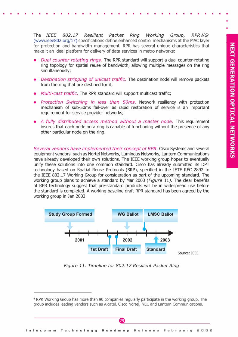
I n f o c o m m T e c h n o l o g y R o a d m a p R e l e a s e F e b r u a r y 2 0 0 2
29
NE
XT
GE
NE
RA
TIO
N O
PT
ICA
L NE
TW
OR
KS
The IEEE 802.17 Resilient Packet Ring Working Group, RPRWG4 (www.ieee802.org/17) specications dene enhanced control mechanisms at the MAC layer for protection and bandwidth management. RPR has several unique characteristics that make it an ideal platform for delivery of data services in metro networks:
Dual counter rotating rings. The RPR standard will support a dual counter-rotating ring topology for spatial reuse of bandwidth, allowing multiple messages on the ring simultaneously;
Destination stripping of unicast trafc. The destination node will remove packets from the ring that are destined for it;
Multi-cast trafc. The RPR standard will support multicast trafc;
Protection Switching in less than 50ms. Network resiliency with protection mechanism of sub-50ms fail-over as rapid restoration of service is an important requirement for service provider networks;
A fully distributed access method without a master node. This requirement insures that each node on a ring is capable of functioning without the presence of any other particular node on the ring.
Several vendors have implemented their concept of RPR. Cisco Systems and several equipment vendors, such as Nortel Networks, Luminous Networks, Lantern Communications have already developed their own solutions. The IEEE working group hopes to eventually unify these solutions into one common standard. Cisco has already submitted its DPT technology based on Spatial Reuse Protocols (SRP), specied in the IETF RFC 2892 to the IEEE 802.17 Working Group for consideration as part of the upcoming standard. The working group plans to achieve a standard by Mar 2003 (Figure 11). The clear benets of RPR technology suggest that pre-standard products will be in widespread use before the standard is completed. A working baseline draft RPR standard has been agreed by the working group in Jan 2002.
Source: IEEE
Figure 11. Timeline for 802.17 Resilient Packet Ring
4 RPR Working Group has more than 90 companies regularly participate in the working group. The group includes leading vendors such as Alcatel, Cisco Nortel, NEC and Lantern Communications.
I n f o c o m m T e c h n o l o g y R o a d m a p R e l e a s e F e b r u a r y 2 0 0 2
30
Supplementing and supporting the IEEE 802.17 effort is an industry advocacy group called the Resilient Packet Ring Alliance (www.rpralliance.org) promoting the standardisation of RPR technology. Founded in Jan 2001, its mission is to nurture and help develop abroad market by promoting the proliferation of Resilient Packet Ring into the broadly denednetworking market, including LAN, MAN, and WAN. The RPR Alliance will play an important role in communicating the RPR message to the world, building consensus for the RPR standard, and ensuring interoperability among RPR vendors.
2.3.7 ITU Standards Development on Passive Optical Network (PON)
Broadband Passive Optical Network (BPON). This standard is commonly referred as ATM-based (APON), and its development is spearheaded by the Full Services Access Network5 (FSAN) consortium. It denes a basic set of common requirements for broadband access systems to support a full range of integrated broadband and narrowband services. The wavelength window in the recommendation species the 1550nm region for downstream and 1310nm region for the upstream direction. The specication was adopted by ITU as G.983.1 in Oct 1998. A related PON management and control interface standard (G.983.2) was later issued in 2000. In Mar 2001, the enhanced Recommendation G.983.3 was completed. It denes a new wavelength allocation by specifying a narrower portion for the downstream window. This portion, referred as basic band, is used for transporting APON downstream signals and the spectral width of 20nm makes it cost effective for using conventional distributed feedback laser diodes. An additional waveband, known as enhancement band, is specied with 2 options available i.e. 1539-1565nm and 1550-1560nm.
Another two draft standards for increasing the efciency and survivability of bre access networks were later adopted by ITU in Nov 2001. G.983.4 species a Dynamic Bandwidth Assignment (DBA) mechanism which improves the efciency of the PON by dynamically adjusting the bandwidth among the ONUs, for example, in response to bursty trafc requirements. G.983.5 species a number of protection options for PONs which will enable enhanced survivability. Table 4 summarises the BPON standards development.
2.3 STANDARD DEVELOPMENTS
5 FSAN is an international initiative of 21 telecommunication operators working together with equipment suppliers. As of November 2001, its members includes Bell Canada, Bell South, Qwest, SBC, Verizon, BT, DTAG, Eire, FT/CNET, KPN, Malta, SwissCom, Telefonica, Telia, TI/CSELT, Bezeq, Chunghwa, KT, NTT, SingTel and Telstra. For more information, please visit FSAN website: http://www.fsanet.net/
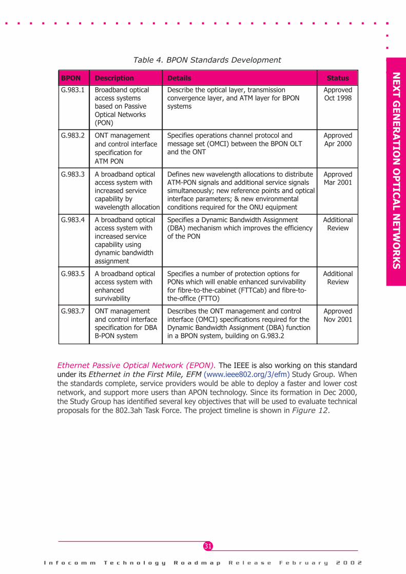
I n f o c o m m T e c h n o l o g y R o a d m a p R e l e a s e F e b r u a r y 2 0 0 2
31
NE
XT
GE
NE
RA
TIO
N O
PT
ICA
L NE
TW
OR
KS
Table 4. BPON Standards Development
Ethernet Passive Optical Network (EPON). The IEEE is also working on this standard under its Ethernet in the First Mile, EFM (www.ieee802.org/3/efm) Study Group. When the standards complete, service providers would be able to deploy a faster and lower cost network, and support more users than APON technology. Since its formation in Dec 2000, the Study Group has identied several key objectives that will be used to evaluate technical proposals for the 802.3ah Task Force. The project timeline is shown in Figure 12.
BPON Description Details Status
G.983.1 Broadband opticalaccess systemsbased on PassiveOptical Networks(PON)
Describe the optical layer, transmissionconvergence layer, and ATM layer for BPONsystems
ApprovedOct 1998
G.983.2 ONT managementand control interfacespecification forATM PON
Specifies operations channel protocol andmessage set (OMCI) between the BPON OLTand the ONT
ApprovedApr 2000
G.983.3 A broadband opticalaccess system withincreased servicecapability bywavelength allocation
Defines new wavelength allocations to distributeATM-PON signals and additional service signalssimultaneously; new reference points and opticalinterface parameters; & new environmentalconditions required for the ONU equipment
ApprovedMar 2001
G.983.4 A broadband opticalaccess system withincreased servicecapability usingdynamic bandwidthassignment
Specifies a Dynamic Bandwidth Assignment(DBA) mechanism which improves the efficiencyof the PON
AdditionalReview
G.983.5 A broadband opticalaccess system withenhancedsurvivability
Specifies a number of protection options forPONs which will enable enhanced survivabilityfor fibre-to-the-cabinet (FTTCab) and fibre-to-the-office (FTTO)
AdditionalReview
G.983.7 ONT managementand control interfacespecification for DBAB-PON system
Describes the ONT management and controlinterface (OMCI) specifications required for theDynamic Bandwidth Assignment (DBA) functionin a BPON system, building on G.983.2
ApprovedNov 2001
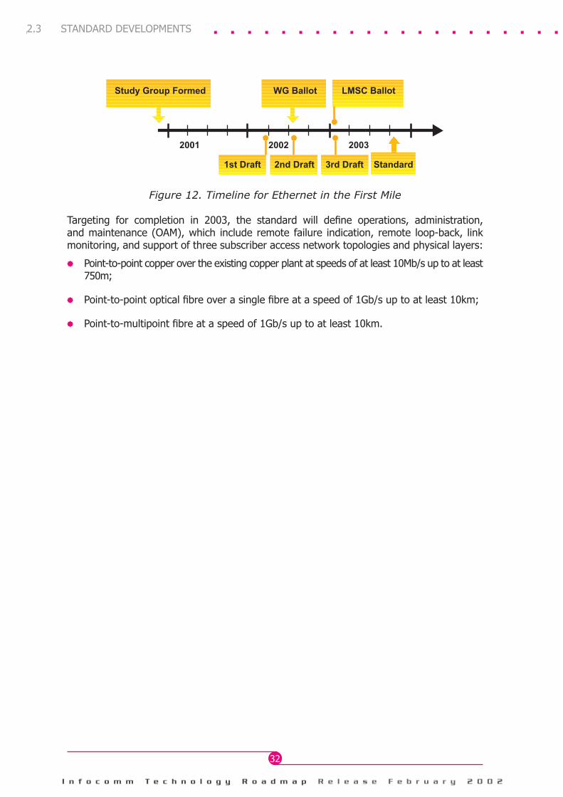
I n f o c o m m T e c h n o l o g y R o a d m a p R e l e a s e F e b r u a r y 2 0 0 2
32
Figure 12. Timeline for Ethernet in the First Mile
Targeting for completion in 2003, the standard will dene operations, administration, and maintenance (OAM), which include remote failure indication, remote loop-back, link monitoring, and support of three subscriber access network topologies and physical layers:
Point-to-point copper over the existing copper plant at speeds of at least 10Mb/s up to at least 750m;
Point-to-point optical bre over a single bre at a speed of 1Gb/s up to at least 10km;
Point-to-multipoint bre at a speed of 1Gb/s up to at least 10km.
2.3 STANDARD DEVELOPMENTS

I n f o c o m m T e c h n o l o g y R o a d m a p R e l e a s e F e b r u a r y 2 0 0 2
33
NE
XT
GE
NE
RA
TIO
N O
PT
ICA
L NE
TW
OR
KS

I n f o c o m m T e c h n o l o g y R o a d m a p R e l e a s e F e b r u a r y 2 0 0 2
34
3 PHOTONICS ENABLING TECHNOLOGIES
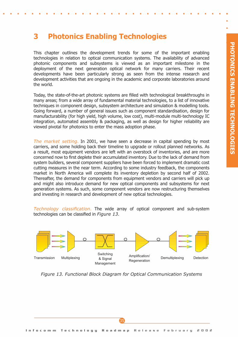
I n f o c o m m T e c h n o l o g y R o a d m a p R e l e a s e F e b r u a r y 2 0 0 2
35
PH
OT
ON
ICS
EN
AB
LING
TE
CH
NO
LOG
IES
3 Photonics Enabling Technologies
This chapter outlines the development trends for some of the important enabling technologies in relation to optical communication systems. The availability of advanced photonic components and subsystems is viewed as an important milestone in the deployment of the next generation optical network for many carriers. Their recent developments have been particularly strong as seen from the intense research and development activities that are ongoing in the academic and corporate laboratories around the world.
Today, the state-of-the-art photonic systems are lled with technological breakthroughs in many areas; from a wide array of fundamental material technologies, to a list of innovative techniques in component design, subsystem architecture and simulation & modelling tools. Going forward, a number of general issues such as component standardisation, design for manufacturability (for high yield, high volume, low cost), multi-module multi-technology IC integration, automated assembly & packaging, as well as design for higher reliability are viewed pivotal for photonics to enter the mass adoption phase.
The market setting. In 2001, we have seen a decrease in capital spending by most carriers, and some holding back their timeline to upgrade or rollout planned networks. As a result, most equipment vendors are left with an overstock of inventories, and are more concerned now to rst deplete their accumulated inventory. Due to the lack of demand from system builders, several component suppliers have been forced to implement dramatic cost cutting measures in the near term. According to some industry feedback, the components market in North America will complete its inventory depletion by second half of 2002. Thereafter, the demand for components from equipment vendors and carriers will pick up and might also introduce demand for new optical components and subsystems for next generation systems. As such, some component vendors are now restructuring themselves and investing in research and development of new optical technologies.
Technology classication. The wide array of optical component and sub-system technologies can be classied in Figure 13.
Figure 13. Functional Block Diagram for Optical Communication Systems
Transmission MultiplexingSwitching& Signal
Management
Amplification/Regeneration
Demultiplexing Detection
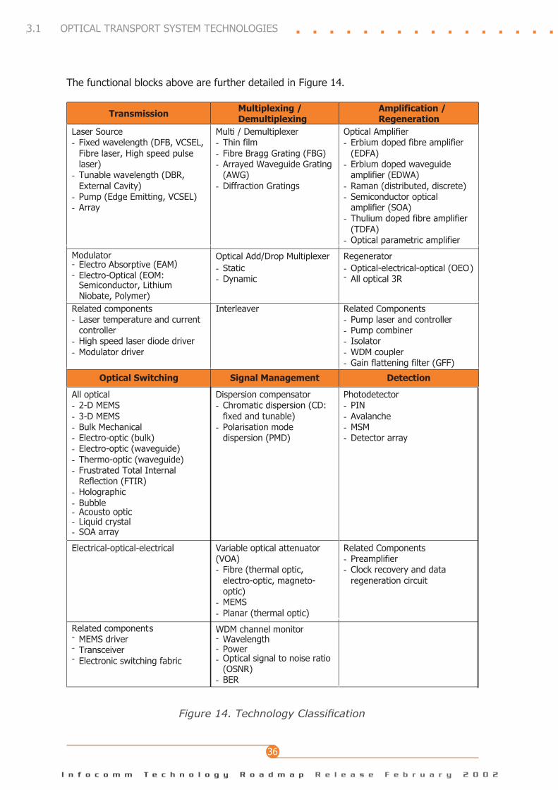
I n f o c o m m T e c h n o l o g y R o a d m a p R e l e a s e F e b r u a r y 2 0 0 2
36
The functional blocks above are further detailed in Figure 14.
Figure 14. Technology Classication
3.1 OPTICAL TRANSPORT SYSTEM TECHNOLOGIES
Transmission Multiplexing /Demultiplexing
Amplification /Regeneration
Laser Source- Fixed wavelength (DFB, VCSEL,
Fibre laser, High speed pulselaser)
- Tunable wavelength (DBR,External Cavity)
- Pump (Edge Emitting, VCSEL)- Array
Multi / Demultiplexer- Thin film- Fibre Bragg Grating (FBG)- Arrayed Waveguide Grating
(AWG)- Diffraction Gratings
Optical Amplifier- Erbium doped fibre amplifier
(EDFA)- Erbium doped waveguide
amplifier (EDWA)- Raman (distributed, discrete)- Semiconductor optical
amplifier (SOA)- Thulium doped fibre amplifier
(TDFA)- Optical parametric amplifier
Modulator- Electro Absorptive (EAM)- Electro-Optical (EOM:
Semiconductor, LithiumNiobate, Polymer)
Optical Add/Drop Multiplexer- Static- Dynamic
Regenerator- Optical-electrical-optical (OEO)- All optical 3R
Related components- Laser temperature and current
controller- High speed laser diode driver- Modulator driver
Interleaver Related Components- Pump laser and controller- Pump combiner- Isolator- WDM coupler- Gain flattening filter (GFF)
Optical Switching Signal Management Detection
All optical- 2-D MEMS- 3-D MEMS- Bulk Mechanical- Electro-optic (bulk)- Electro-optic (waveguide)- Thermo-optic (waveguide)- Frustrated Total Internal
Reflection (FTIR)- Holographic- Bubble- Acousto optic- Liquid crystal- SOA array
Dispersion compensator- Chromatic dispersion (CD:
fixed and tunable)- Polarisation mode
dispersion (PMD)
Photodetector- PIN- Avalanche- MSM- Detector array
Electrical-optical-electrical Variable optical attenuator(VOA)- Fibre (thermal optic,
electro-optic, magneto-optic)
- MEMS- Planar (thermal optic)
Related Components- Preamplifier- Clock recovery and data
regeneration circuit
Related components- MEMS driver- Transceiver- Electronic switching fabric
WDM channel monitor- Wavelength- Power- Optical signal to noise ratio
(OSNR)- BER
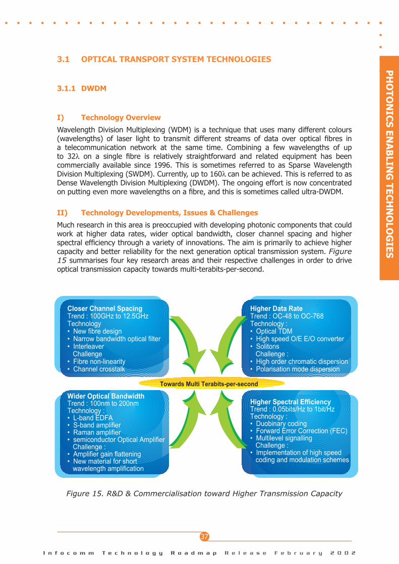
I n f o c o m m T e c h n o l o g y R o a d m a p R e l e a s e F e b r u a r y 2 0 0 2
37
PH
OT
ON
ICS
EN
AB
LING
TE
CH
NO
LOG
IES
3.1 OPTICAL TRANSPORT SYSTEM TECHNOLOGIES
3.1.1 DWDM
I) Technology Overview
Wavelength Division Multiplexing (WDM) is a technique that uses many different colours (wavelengths) of laser light to transmit different streams of data over optical bres in a telecommunication network at the same time. Combining a few wavelengths of up to 32λ on a single bre is relatively straightforward and related equipment has been commercially available since 1996. This is sometimes referred to as Sparse Wavelength Division Multiplexing (SWDM). Currently, up to 160λ can be achieved. This is referred to as Dense Wavelength Division Multiplexing (DWDM). The ongoing effort is now concentrated on putting even more wavelengths on a bre, and this is sometimes called ultra-DWDM.
II) Technology Developments, Issues & Challenges
Much research in this area is preoccupied with developing photonic components that could work at higher data rates, wider optical bandwidth, closer channel spacing and higher spectral efciency through a variety of innovations. The aim is primarily to achieve higher capacity and better reliability for the next generation optical transmission system. Figure 15 summarises four key research areas and their respective challenges in order to drive optical transmission capacity towards multi-terabits-per-second.
Figure 15. R&D & Commercialisation toward Higher Transmission Capacity
I n f o c o m m T e c h n o l o g y R o a d m a p R e l e a s e F e b r u a r y 2 0 0 2
38
Closer Channel Spacing. Higher transmission capacity can be achieved by increasing the density of multiplexing, i.e. narrowing the separation between adjacent optical signals from the standard 100GHz and towards 12.5GHz in the future. To pack more channels in the much narrower spacing, researchers will have to overcome a series of technical challenges. Amongst these challenges include narrow bandwidth and low crosstalk optical lter design and laser diode wavelength stabilisation. One approach to alleviate the requirement on optical lter design is to use interleavers together with optical lters. This allows closer channel spacing and at the same time provides a smooth upgrading path. Currently, we are beginning to see more commercial WDM products using channel spacing of 50GHz. More 25GHz channel spacing WDM system is envisaged to enter commercialisation in the near term, while 12.5GHz system would not be available anytime soon.
Higher Data Rate, 80-160Gb/s. The light beam sent from the laser diode transmitter must be modulated at a higher speed in order to increase the data rate of a single optical signal. This means that the circuit driving the modulator must be capable of running at speeds greater than the current maximum of 40Gb/s. American, European and Japanese component manufacturers are competing to develop modulators and drive circuits needed to accomplish this. Material technologies such as Gallium Arsenide (GaAs) and Indium Phosphide (InP) are used for this application because they can be driven at high speed.
Another way to increase the speed of a single wavelength beyond 40Gb/s is to use Optical Time Division Multiplexing (OTDM). It combines different stream of optical signals of the same wavelength via optical means into a high data-rate bit stream. Companies such as NTT and Nortel Networks are actively pursuing OTDM technology. OTDM runs electronic circuits such as modulators and drivers in parallel, modulating optical signals at a given frequency with small differences in timing, then multiplexing them into light. With four circuits in parallel, each modulating at 40Gb/s, an optical signal with a capacity of 160Gb/s would be generated. OTDM can be used together with WDM technology to increase the overall capacity of the network. However, due to difculty with synchronisation and complexity in the multiplexing and demultiplexing system, OTDM is still not widely used except in some test and measurement systems. Statistical OTDM is also known as optical packet switching. It enables a better utilisation of the capacity provided by a single wavelength channel. True all optical packet routing may however be many years away, as the technologies to recognise optical packet headers and to process them have only been demonstrated in the labs.
Wider Optical Bandwidth. Currently C-band (1530-1565nm) and L-band (1570-1610nm) are widely used in optical communication. The third waveband, S-band (1480nm-1530nm) is also being explored. With a wider bandwidth to multiplex optical signals, the number of wavelengths can be raised, thus increasing the transmission capacity. Using any wavelengths other than the current C- or L-bands, however, will make it difcult to maintain long-distance performance due to losses of optical bre. To keep performance in long-distance transmission, optical bre ampliers based on Er doping are now used to increase the transmission distances for C- and L-bands. Er has the property of amplifying optical signals in frequencies around the C-band, but not in the S-band. These optical bre ampliers however are necessary in the transmission path to amplify attenuated optical signals to make long-haul networks possible. Therefore, Raman amplier and other new types of ampliers such as Thulium doped bre amplier have to be used to make S-band transmission possible.
3.1 OPTICAL TRANSPORT SYSTEM TECHNOLOGIES

I n f o c o m m T e c h n o l o g y R o a d m a p R e l e a s e F e b r u a r y 2 0 0 2
39
PH
OT
ON
ICS
EN
AB
LING
TE
CH
NO
LOG
IES
Higher Spectral Efciency. Another way to increase the transmission speed over a given optical bandwidth is to increase spectral efciency i.e. to pack more bits into a given optical bandwidth. This can be achieved using new coding scheme such as duobinary coding and multilevel signalling. However, these require more complex signal processing at the receiver. For example, multilevel signal detection may be required. This not only implies more complex electronics, but also reduced noise margin.
WDM, DWDM, and their future technological advancement, ultra-dense wavelength division multiplexing (UDWDM), have allowed the transmission capacity of optical bre to increase rapidly.
Figure 16 envisages the development trend in WDM transmission capacity over the next ve years. Initially, WDM allowed the number of wavelengths carried on a single bre to quickly increase from 8 to 16 to 32λ. With DWDM, the gure has risen to around 160. Soon, UDWDM will up the ante even more, supporting about 400 wavelengths. The state-of-the-art now is between 80λ to 160λ on a single bre. By 2003, we envisaged that 256λ would be achievable, employing 10Gb/s and limited 40Gb/s data rates using TDM. It is expected that upward of 1000λ would eventually become possible by 2006, using mostly 40Gb/s data rates. This will permit a dozen of terabits-per-second of data to be transmitted over a single bre. Beyond this timeline, we postulate that OTDM would start its initial phase of deployment into the optical space with the introduction of 80/160Gb/s data rate systems.
Figure 16. Development scenario of commercial WDM Systems
Most commercial DWDM systems6 today can offer up to 1.6Tb/s. At the same time, experimental trials7 from NEC and Alcatel have already achieved 10Tb/s region in a single bre over more than 100km, employing a total of 273 wavelengths.
OverallTransmissionCapacity
OTDM Linebit-rate
TDM Linebit-rate
Operating bandNo. of Channel
ChannelSpacing
90s 2000 2003 2006
20Gb/s 1 to 5 Tb/s 5 to 10 Tb/s >10 Tb/s
TDM (2.5Gb/s) TDM (2.5 to 10 Gb/s) TDM (10 to 40 Gb/s) TDM (40 Gb/s)
OTDM(>80Gb/s)
200GHz 100 to 50GHz 50 to 25GHz 25 to 12.5GHz
C band(8 to 40 )
C, L band(up to 160 )
C, L band(256 to 400 )
C, L,S band(up to 1000 )
6 Few examples: Lucent’s WaveStar™ OLS 1.6T (www.lucent.com/businesspartners/clp/webcast/010403.html); Marconi’s SmartPhotoniX™ UPLx160™ (www.marconi.com/html/news/marconiintroducessolitonbasedultralonghaulsystem.htm);Nortel Network’s OPTera Long-Haul 1600 (www.nortelnetworks.com/products/01/optera/long_haul/1600/index.html)
I n f o c o m m T e c h n o l o g y R o a d m a p R e l e a s e F e b r u a r y 2 0 0 2
40
The market for DWDM equipment can be generally considered pessimistic in 2001 but reasonably optimistic thereafter according to Cahners In-Stat Group. In the long-haul market, In-Stat reported a 22-24% decline for 2001 as compared to 2000. A single digit growth is however expected in second half of 2002 for the long-haul market. Despite the economic downturn, the market for this network segment will continue to be robust. China would continue to provide much needed impetus for growth for Asia. The more popular practical demand for metro DWDM systems in the next 5 years will gear towards 10Gb/s and 40Gb/s optical systems. In-Stat foresees a good DWDM market from 2002 to 2005. The total long-haul and metro DWDM global market is forecasted to be worth US$16 billion in 2005.
3.1.2 Soliton Transmission
I) Technology Overview
In conventional DWDM transmission system, optical ampliers are used to boost the optical signals, typically every 60 to 100km. However, every one to two thousand kilometres, optical signals need to be fully regenerated to remove the effects of noise and other transmission impairments. Without all optical regeneration, which is still very difcult at the moment, we need a lot of expensive equipments to convert the light to electrical signal so that each wavelength channel can be process individually. One way to extend the span between regenerators is to use soliton transmission. Solitons are light pulses that maintain their shape even when transmitted over very long distances. They actually leverage on the non-linear effects that occur in the bre, self-phase modulation (SPM), and on the linear effects, chromatic dispersion, to offset each other resulting in enhanced performance. Put simply, solitons are an alternative efcient method of encoding or modulating a digital signal over long-haul system.
II) Technology Developments, Issues & Challenges
Continual research has yielded newer and more practical variations of solitons. One variation, called dispersion-managed soliton, retains the benet of attaining long reach transmission of classical soliton while improving spectral efciency and compatibility with the wide range of bre types in use today. As a result conventional DWDM system can easily be upgraded to soliton-based DWDM system without changing the network architecture. The only change is a drastic reduction in the number of regenerators. This is particular suitable for long-haul transmission system. Since if there is no regenerator in the transmission system, the capacity can easily be increased by adding soliton signalsat different wavelengths without the need to change anything in between. Experimental soliton systems have achieved all-optical transmission distances of 20,000 km, more than twice the Trans-Pacic distance.
7 NEC Press, 22 March 2001: http://www.nec.co.jp/english/today/newsrel/0103/2201.html & Alcatel Press, 21 March 2001: http://www.alcatel.com/vpr/?body=/latestnews/21032001uk
3.1 OPTICAL TRANSPORT SYSTEM TECHNOLOGIES
I n f o c o m m T e c h n o l o g y R o a d m a p R e l e a s e F e b r u a r y 2 0 0 2
41
PH
OT
ON
ICS
EN
AB
LING
TE
CH
NO
LOG
IES
Solitons have many other real world advantages over more traditional modulation methods. For example, solitons could be used to increase transmission speed up to 40Gb/s, or OC-768, and possibly beyond. This is due to its resistance to chromatic dispersion (CD) and polarisation mode dispersion (PMD) which are major limiting factors in high-speed optical transmission systems. A single wavelength soliton transmission at 80Gb/s had been demonstrated. This could make a good alternative for carriers whose installed base of bre could not easily support high number of DWDM channels.
There are several challenges that remain in the near term which must be addressed before solitons can be applied effectively. A major challenge is that enabling the functioning of solitons involves working with a signal that is signicantly more intense than typical existing systems. This translates into a shorter amplier spacing of between 10 to 50 km, which is one of the major practical problems of soliton transmission. A high power gain to maintain the soliton effect is probably not what the service providers would wish for in its effort to cut costs. There are also other issues, such as the development of rened control techniques capable of separating solitons by several times their pulse width so as to enable practical applications in a telecommunication system. The ability to master and regulate slight differences in soliton amplitudes is also important. In addition, to harness the exceptional transmission speed of solitons, researchers must be able to create synchronous amplitudes as well as phase modulation with optical ltering. As soon as these specic issues are resolved, a new generation of transmission based on soliton waves could become practical.
Being a relatively new technology, there are fewer market gures to share. Few soliton-based commercial products are only starting to enter the market. Marconi UPLx160, a soliton-based technology which offers a capacity of 1.6Tb/s; 160 wavelengths at 10Gb/s per wavelength for up to 3,000km without signal regeneration. Lucent and Nortel Networks are also lining up commercial soliton-based products.
3.1.3 Optical Regeneration
I) Technology Overview
In an optical transmission system, an optical signal is attenuated and distorted due to attenuation, dispersion, crosstalk and non-linearity associated with optical bres and other components in the system. Since the effects are accumulative, optical signal regeneration is needed. Three types of regeneration are possible: 1R (re-amplication), 2R (re-amplication & re-shaping) and 3R (re-amplication, re-shaping & re-timing). Currently 1R is generally done optically while 2R and 3R are carried out using O/E, E/O converters and electronic regenerators. With the increase in transmission speed in a single wavelength, especially when OTDM is used more widely, there is a greater need for all these to be done optically.
II) Technology Developments, Issues & Challenges
1R regeneration. A simple form of regeneration is amplication. It restores the signal level and can be easily accomplished using various types of optical amplier. The amplication is not dependent on bit rate and data format, and all the WDM channels can be amplied simultaneously. However, crosstalk is also amplied and noise is added.
I n f o c o m m T e c h n o l o g y R o a d m a p R e l e a s e F e b r u a r y 2 0 0 2
42
2R regeneration. Another level of regeneration is amplication and reshaping. It suppresses crosstalk and noise such as amplied spontaneous emission (ASE) noise introduced by optical ampliers. A decision element with a threshold function is required. Currently it is typically done electronically through the use of O/E and E/O conversion and electronic regenerator. It is also possible to do it optically through the use of saturable absorber or SOA based interferometer. However, the technology is still not mature enough to be used in commercial systems. No matter optical or electrical 2R regeneration is used, WDM channels have to be regenerated individually.
3R regeneration. Like all the other digital communication systems, ultimately 3R regeneration (amplication, reshaping and retiming) is necessary over a certain transmission distance to eliminate the signal degradation. If 3R signal regeneration interval is small enough, complete error free transmission is possible. In commercial systems this is now done electronically. To do it optically, optical clock recovery and decision circuit needs to be implemented. The decision circuit will be a nonlinear gate. Recovered optical clock is used to sample the data stream through the nonlinear gate. Since the switching window of the data driven gate is larger than the pulse width of the optical clock, jitter of data and switching window are not transferred to the transmitted clock pulses. The shape of the regenerated pulses is dened by the shape of the clock pulses. Mode locked laser, self-pulsating DFB laser and Fabry Perot optical lter can all be used for clock recovery function. While mode locked laser, self-pulsating DFB laser, active optical interferometer and nonlinear optical loop mirror can be used as decision circuits. All techniques have been demonstrated experimentally, however, they are still in the early stages of research. It will be a few years before the system can be commercially viable.
3.2 ACTIVE COMPONENTS & SUB-SYSTEMS
3.2.1 Lasers
I) Technology Overview
All optical networks require extensive use of optical transmitters and receivers (or integrated as transceivers). These comprise laser transmitters and photo-detectors respectively.
A laser is a device that creates and amplies a narrow, intense beam of coherent light. Ever since its inception, various types of lasers have emerged, from the conventional gas lasers to solid-state to the emerging tunable diode lasers. Currently, lasers operating at wavelengths around 850nm, 1310nm and 1550nm are used for bre optic transmission systems while pump lasers at 980nm and 1480nm are used in optical ampliers. A trend in the development of laser technology is to reduce the cost of laser so that it can be used more widely for access and data communication applications. This has been led by the development of VCSEL technology.
The common lasers used are either edge emitting lasers or surface emitting lasers. Regardless of the type of lasers preferred, a clear trend in laser technology points towards wideband tunability and cheaper tunable lasers for optical networking in the C- and L-bands, as compared to current xed wavelength lasers. The tuning methods normally used vary from current driven (DBR lasers), to motor driven and more complex MEMS technology (VCSEL and External Cavity lasers).
3.2 ACTIVE COMPONENTS & SUB-SYSTEMS
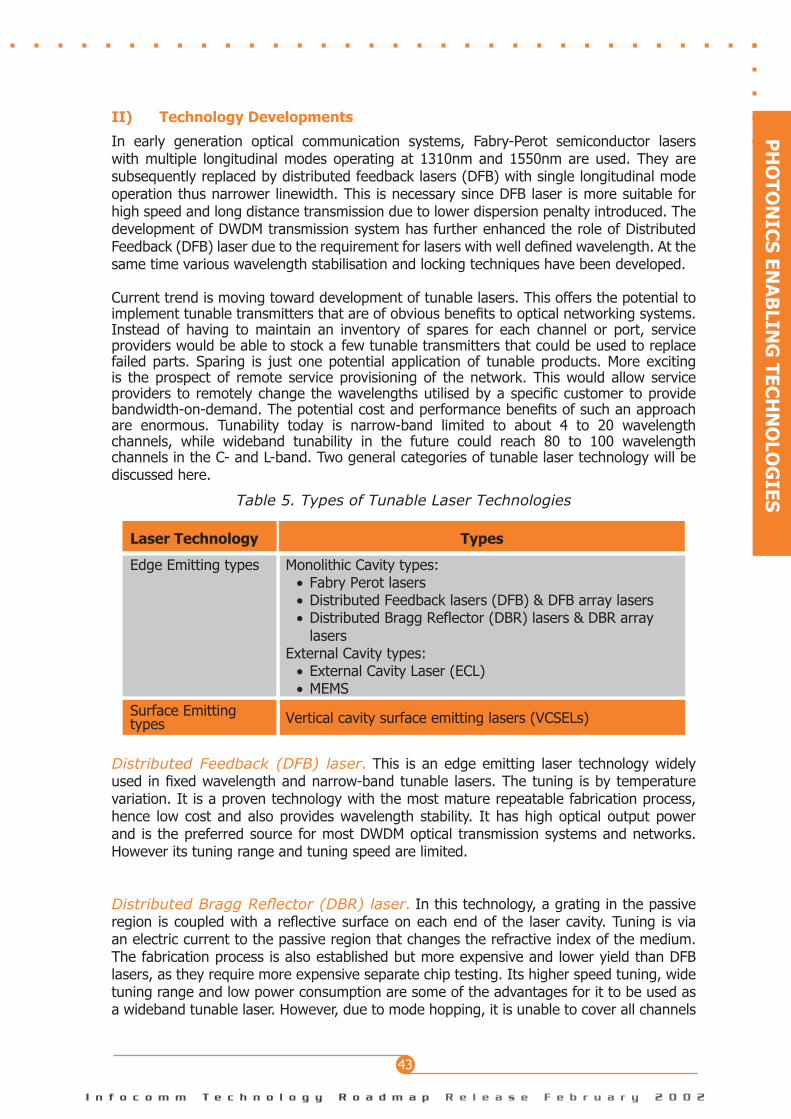
I n f o c o m m T e c h n o l o g y R o a d m a p R e l e a s e F e b r u a r y 2 0 0 2
43
PH
OT
ON
ICS
EN
AB
LING
TE
CH
NO
LOG
IES
II) Technology Developments
In early generation optical communication systems, Fabry-Perot semiconductor lasers with multiple longitudinal modes operating at 1310nm and 1550nm are used. They are subsequently replaced by distributed feedback lasers (DFB) with single longitudinal mode operation thus narrower linewidth. This is necessary since DFB laser is more suitable for high speed and long distance transmission due to lower dispersion penalty introduced. The development of DWDM transmission system has further enhanced the role of Distributed Feedback (DFB) laser due to the requirement for lasers with well dened wavelength. At the same time various wavelength stabilisation and locking techniques have been developed.
Current trend is moving toward development of tunable lasers. This offers the potential to implement tunable transmitters that are of obvious benets to optical networking systems. Instead of having to maintain an inventory of spares for each channel or port, service providers would be able to stock a few tunable transmitters that could be used to replace failed parts. Sparing is just one potential application of tunable products. More exciting is the prospect of remote service provisioning of the network. This would allow service providers to remotely change the wavelengths utilised by a specic customer to provide bandwidth-on-demand. The potential cost and performance benets of such an approach are enormous. Tunability today is narrow-band limited to about 4 to 20 wavelength channels, while wideband tunability in the future could reach 80 to 100 wavelength channels in the C- and L-band. Two general categories of tunable laser technology will be discussed here.
Table 5. Types of Tunable Laser Technologies
Distributed Feedback (DFB) laser. This is an edge emitting laser technology widely used in xed wavelength and narrow-band tunable lasers. The tuning is by temperature variation. It is a proven technology with the most mature repeatable fabrication process, hence low cost and also provides wavelength stability. It has high optical output power and is the preferred source for most DWDM optical transmission systems and networks. However its tuning range and tuning speed are limited.
Distributed Bragg Reector (DBR) laser. In this technology, a grating in the passive region is coupled with a reective surface on each end of the laser cavity. Tuning is via an electric current to the passive region that changes the refractive index of the medium. The fabrication process is also established but more expensive and lower yield than DFB lasers, as they require more expensive separate chip testing. Its higher speed tuning, wide tuning range and low power consumption are some of the advantages for it to be used as a wideband tunable laser. However, due to mode hopping, it is unable to cover all channels
Laser Technology Types
Edge Emitting types Monolithic Cavity types:• Fabry Perot lasers• Distributed Feedback lasers (DFB) & DFB array lasers• Distributed Bragg Reflector (DBR) lasers & DBR array
lasersExternal Cavity types:
• External Cavity Laser (ECL)• MEMS
Surface Emittingtypes Vertical cavity surface emitting lasers (VCSELs)
I n f o c o m m T e c h n o l o g y R o a d m a p R e l e a s e F e b r u a r y 2 0 0 2
44
on the ITU grid. It also suffers from wavelength instability, that hopefully, with technology maturity, we will see better performance enhancements.
External Cavity laser (ECL). The tuning is achieved using mechanical means i.e. by adjusting the physical length of the laser cavity, hence tuning the wavelength of the output beam. ECLs comprise of a separate external gain cavity, hence its name. The advantages of this technology include high optical output power (favouring long-haul), wavelength stability, continuous tuning and low noise. However, it may be bulky and has lower tuning speed.
Vertical Cavity Surface Emitting Laser (VCSEL). These are surface emitting lasers with a vertical laser cavity. VCSEL can use MEMS as mirror to reect light, and can be electrically or optically pumped. The advantages of VCSEL technology are its low manufacturing costs and can be easily integrated with other devices. However, current VCSEL products still have lower optical output power and slower switching speed when compared with other competing edge emitting laser technologies. Hence most VCSELs are currently used in MANs.
Researchers have been working for years to create laser that works like LED, emitting light out of the wafer, perpendicular to the surface. Instead of coated mirrors on the cavity, it uses epitaxial layers grown on the wafer to create mirrors on the surface with LED sandwiched in between. These epitaxial layers can create lenses to focus light into a tight cone, perfect for coupling to bres. There are in fact varied structures of VCSEL diodes available - planar proton implanted, index guided ridge waveguide, hybrid mirror, intro cavity, lateral oxide, native oxide, wafer bonded, but so far only proton implanted, ridge waveguide and oxide conned structures are available commercially.
One of the biggest advantages of VCSEL is that testing can be done prior to dicing, a major saving in cost during manufacturing. A completed wafer can be tested in a wafer probe machine, where each device is contacted by microscopic electrical probes and current applied. If it is good, it can be seen on a camera and measured. Thus good devices can be detected before the wafer is diced and bad ones marked automatically for discard.
Another advantage of VCSELs is that their size and light emitting properties are suitable to build inline and 2-D laser-diode arrays. The inline array is useful as the source for parallel optical interconnects, which use a at cable similar to copper at cable but with optical bre in place of copper. This type of cabling has applications in short-distance chassis or board interconnects and can provide a system designer with high aggregate data rates.
However, VCSELs are not yet available at the most popular wavelengths for optical communication. 850nm & 980nm VCSELs are now commercially available, but the 1310nm/1550nm devices are just being developed in labs. We expect the latter to be commercialised from earliest 2003. Also, there is a need to develop VCSEL for high-power applications, which currently can only be met by edge emitting laser diodes.
Market Outlook. Despite cautioning on the slowdown of the component market, several consultancy rms have forecasted favourable market sizes for tunable lasers. According to the Yankee Group, the worldwide market for tunable lasers would be worth US$413 million in 2003, and US$2.3 billion in 2005.
3.2 ACTIVE COMPONENTS & SUB-SYSTEMS
I n f o c o m m T e c h n o l o g y R o a d m a p R e l e a s e F e b r u a r y 2 0 0 2
45
PH
OT
ON
ICS
EN
AB
LING
TE
CH
NO
LOG
IES
Narrowband Tunable Lasers. Alcatel Optronics, JDS Uniphase, Nortel and Bragg Photonics are shipping DFB lasers while Agere and Marconi are shipping DBR lasers. Many of these tunable lasers are still considered narrow-band. Some equipment and system vendors like Fujitsu are already shipping equipment based on these narrowband tunable lasers in their DWDM products. Others like Ciena expect to do so in mid 2002 while currently actively testing with both narrowband and wideband tunable lasers. The market today, according to CIR, is still mainly dominated by DFB lasers, which make up almost the entire market for tunable lasers in 2001, but projected to drop to about 80% market share in 2002.
Wideband Tunable Lasers. ADC and Agility are shipping wideband tunable lasers while Marconi’s products would be available in mid 2002. Bragg Photonics is also developing wideband tunable lasers based on DFB lasers. Iolon is shipping External Cavity lasers while New Focus is in sample production of such lasers. Blue Sky Systems, a subsidiary of Blue Sky Research in the US, has developed programmable lasers for generating ITU wavelengths, based on a high-power, low-cost 1550nm laser diode with a proprietary compact external-cavity design. This provides a high power, high tuning speed, wideband (C- & L-band), small size and low-cost laser. Initial samples with 10-15mW and millisecond tuning speeds from Blue Sky Research will see the light in 2002. Bandwidth9 is in pilot production of VCSEL tunable lasers while Nortel is in sampling production of tunable lasers based on VCSELs.
3.2.2 Optical Ampliers
I) Technology Overview
An optical signal experiences attenuation as it propagates through an optical bre. Hence, an optical transmission system must be carefully designed to ensure that there is adequate signal strength for detection at the receiver end. We will discuss various optical amplier technologies in the following sections.
II) Technology Developments, Issues & Challenges
Erbium-doped Fibre Amplier (EDFA). Direct optical amplication via EDFAs was rst developed to replace the need for costly electrical regeneration of an optical signal. Carriers can realise savings not only by reducing the amount of TDM equipment required, but often by eliminating the need to build intermediate regenerator sites with their associated power, climate control, maintenance, and security costs. In recent years, the EDFA has evolved into a low cost enabling technology for DWDM as the market demand for capacity grows. The following EDFAs are discussed:
Silica-based EDFA. Amplifying a DWDM signal with a traditional silica-based EDFA poses some technological challenges due to the fact that the gain curve is not at over the desired operating band. This resulted in some channels retaining a relatively strong optical signal to noise ratio (OSNR), whereas others, especially in the 1540nm region, encounter serious signal to noise erosion. This degradation can be so severe that these channels no longer offer an adequate OSNR. Gain equalisation to atten the gain has to be carried out;
I n f o c o m m T e c h n o l o g y R o a d m a p R e l e a s e F e b r u a r y 2 0 0 2
46
Fluoride EDFA, the Flat Gain EDFA. The usable bandwidth in a long cascading chain of EDFAs can be signicantly increased by using ampliers with atter gain spectrum. For systems that require 100 or more channels, designers have to make use of the complete C- and L-bands. There are two basic approaches to attening the gain spectrum. The rst approach involves tailoring the material properties of the erbium-doped bre, either with the addition of extra dopants such as aluminium, or going to an altogether different host material, such as uoride-based bre instead of silica. While aluminium co-doping broadens the gain, the main peak at 1530nm still remains. With high power ampliers that require multiple pumps, each amplier might need a new bre design, adding to time, cost and uncertainty;
On the other hand, the main problem with uoride-based bre is reliability issue. Fluoride-based bre is sensitive to moisture and is very difcult to splice onto standard single mode bre. One other performance drawback of the uoride EDFA is the higher noise gure, a result of being pumped at 1480nm. There are ways to overcome this inherent weakness and vendors are beginning to offer next generation uoride EDFAs that provide both at gain and low noise gure.
Other Gain Flattening Techniques for EDFA. Besides doping, another approach is to use an external gain-attening lter. The principle of gain attening is conceptually quite simple: lters are designed to approximate the inverse characteristics of the EDFA gain spectrum. The effectiveness of any gain at lter is therefore dependent on the degree to which it can approximate the inverse gain characteristics. Since the gain curve of an EDFA depends on the input power, in an optical network environment where channels are added and dropped dynamically, dynamic gain equalisation and control are required. We will elaborate more on the application of gain attening lters for optical ampliers in the passive components section.
Thulium-doped Fibre Amplier (TDFA) in S-Band. The number of channels available in the existing bandwidth regions (C-band and L-band) for optical communications is already near saturation. In search for new regions, the S-band has been viewed as a promising candidate, pending the development of products covering this region such as light sources for measuring & testing, and more efcient optical ampliers. Doping with Tm in the S-band is attracting much attention as it offers similar optical amplication as Erbium (Er) in the C- and L-band. Tm is a rare earth located next to Er in the periodic table. With Tm, it is possible to build an optical bre amplier that functions in the S-band, and research into this eld is under way at NTT, NEC and Hitachi. For information, NEC implemented 85 channels in the S-band in addition to the 92 channels in the C-band and 96 channels in the L-band to achieve a world record 10.92Tb/s transmission over more than 100 km. The key problem with Tm is its rarity, and some in the industry are concerned with obtaining a stable supply of Tm.
Raman Amplication. Raman amplication is another optical bre amplication technology that can also handle S-band, without relying on elements such as Tm. Unlike Er and Tm, Raman amplier can be used in all wavebands. In addition, its ability to provide distributed amplication results in an improved signal-to-noise ratio performance and reduced bre non-linearity effects. Raman amplier has been studied long before EDFA, however, it has only been used in practical systems recently. This is mainly attributed to the development in high power bre laser, high power diode laser and pump combiners. Raman amplier uses the transmission bre itself as the amplication medium. Gain is created
3.2 ACTIVE COMPONENTS & SUB-SYSTEMS

I n f o c o m m T e c h n o l o g y R o a d m a p R e l e a s e F e b r u a r y 2 0 0 2
47
PH
OT
ON
ICS
EN
AB
LING
TE
CH
NO
LOG
IES
due to the conversion of the pump photon to the signal photon, with the simultaneous production of an optical phonon which is the atomic vibration. The efciency is typically low (25% compare with about 80% of EDFA). As a result, high pump power in the range of a few hundred mW to a few watts is typically required. Raman amplication spectrum depends on pump wavelength and pump power and can span from 850nm to 1600nm. Gain equalisation can easily be achieved through the use of a few pump sources at different wavelengths combined together using a pump combiner. By adjusting pump wavelength and pump power of each laser, a at gain over a wide wavelength range can be achieved. It enables ultra long-haul and high bit-rate transmission system. However, due to cost reasons, mixed systems may be used with Erbium doped ampliers at 1530nm region as EDFA technology is currently cheaper.
Other amplication techniques that attract much development interests are Erbium Doped Waveguide Amplier (EDWA) and Semiconductor Optical Amplier (SOA). EDWA uses a few centimetres of highly doped optical waveguide as the gain medium. It can provide a few dB of gain with a noise gure less than 5dB. Since it can be integrated with other components resulting in a compact size, it has very good potential to be used in metropolitan area optical networks. SOA provides good single channel amplication. However, crosstalk and higher noise have prevented it from being used for multichannel WDM signal amplication. In WDM system, it is mainly integrated with the receiver as an optical preamplier. It may also be used in WDM optical add/drop nodes to amplify each wavelength channel to provide gain equalisation and control. It will nd many applications in metropolitan and access networks. In addition, it is also a single most important component for non-linear applications such as wavelength conversion.
Gain Control of Optical Ampliers. Another issue concerning optical ampliers in general is the control of the output power of such devices. Optical ampliers are usually coupled with variable optical attenuators (VOAs) that serve to regulate their output power via tunable gain control. The trend is to produce ampliers with integrated VOAs. The tuning speed of VOAs is in the order of milliseconds in many current systems. However, in a DWDM system, if we encounter breakdown in one of the channels, the gain of this channel is distributed to the remaining channels in nanoseconds. This would result in saturation since the VOAs might not be fast enough to regulate the ampliers. Hence, there is product development interest to look into gain tuning systems that can operate in nanoseconds for optical amplication. Different optical control schemes such as optical feedback control have been studied for this application.
Market Outlook. Optical ampliers are mostly used in long-haul and more recently in metropolitan area networks, hardly in access network. Cahners In-Stat Group estimated that the worldwide market size for such ampliers, based on long-haul and metropolitan area markets, was about US$3.3 billion in 2001 and projected the gure to rise to US$4.7 billion in 2006. Their estimation consisted of new installations, spares, anticipated upgrades to existing systems and the timing of such upgrades. To enable fast adoption of optical ampliers in the metropolitan area network, one important concern is to reduce the cost. This may be achieved through the use of uncooled pump laser in EDFA and through integration of some of the components used in EDFA. Other technologies such as EDWA or SOA may also help to reduce the cost. A few vendors are marketing EDWA now.
I n f o c o m m T e c h n o l o g y R o a d m a p R e l e a s e F e b r u a r y 2 0 0 2
48
3.2.3 Optical Switching
I) Technology Overview
Optical switching or routing refers to the re-directing of an optical signal from one network node to another node. To reach a destination, the signal carrying information hence travels or switches through a series of nodes that then make up the optical path taken by the signal from point A to point B. Two main approaches can be used to implement an optical switch to direct an optical signal from a given input port to a given output port:
Optical-Electrical-Optical (OEO switching). As opposed to OOO switching or rout-ing, an optical signal coming to the input port of an optical switch has to be converted to an electrical signal for conventional electronic switching equipment to understand this signal, and then reconverted to optical signal for re-transmission to the outgoing port. It is also known as an opaque switch because an optical signal cannot pass through an OEO switch without being converted into an electrical signal. This approach offers the advantages of being able to use existing electronic switching technology and the ability of providing 3R regeneration whenever optical signal passes through the switch. However, it does not provide bit rate, service and protocol transparency;
All Optical Switching or (OOO switching). An all optical switch uses all optical means to direct the optical signal from the input port to the output port without chang-ing it to electrical signal. Various technologies can be used to implement the optical switching fabric. It is also known as a transparent switch. It provides bit rate as well as service and protocol transparency. However, it does not offer complete signal regenera-tion and based on current technologies switching speed is still low and size is small.
An optical switch can be used for circuit switching (lambda switching), burst switching and packet switching. In lambda switching optical signal is directed from the input port to the output port based on its wavelength. The connection is typically long and the switching time required is in the order of sub-millisecond. Optical circuit switching network is the form taken by almost all the optical networks now. Optical switches are used in such networks in a few application areas:
Protection Switching. It refers to the automatic switching between bre links, when we encounter for example a breakdown in one of the links. 1x2 optical switch with mil-lisecond switching speed is typically required;
Optical Cross Connect (OXC) or Photonic Cross Connect (PXC). It allows the optical wavelength at an input port to be connected to the same wavelength (or dif-ferent wavelength if wavelength conversion is used) of an output port for provisioning and reconguration of light paths. It is used as an interconnect device between differ-ent WDM ring networks or to create optical mesh backbones. Electrical signals provided by the GMPLS control plane are used to control the switching fabric (OOO or OEO) to provide dynamic lambda switching. Optical switches with large port count are required for this application;
Optical Add-Drop Multiplexer (OADM). The function of an OADM is basically similar to the electrical SONET ADM used today, except that only optical wavelengths of light are added and dropped. It is generally used in a point to point WDM optical link to
3.2 ACTIVE COMPONENTS & SUB-SYSTEMS
I n f o c o m m T e c h n o l o g y R o a d m a p R e l e a s e F e b r u a r y 2 0 0 2
49
PH
OT
ON
ICS
EN
AB
LING
TE
CH
NO
LOG
IES
terminate and reuse an optical wavelength or used in ring based optical network to add or drop wavelength connections.
Optical burst and packet switching are forms of statistical optical TDM. In the former, the goal is to set up the wavelength connection for the duration of a data burst. Burst data need to be buffered at the input of the switch while the wavelength connection is being set up. Very fast switching is required. This is still not easily done all optically (OOO). One possibility is to use SOA arrays. Optical packet switch is essentially the optical equivalent of a electronic packet switch. It needs to read optical header and switch optical packet at very high speed. Both input optical buffer and output optical buffers are required. Although researchers have demonstrated all optical burst and packet switches, they are still not prac-tical today because it is still extremely difcult to recognise or read optical packet headers via entirely optical means. At the same time no good way to buffer optical signal is available today. True all optical packet switching is said to be at least 10 years away for commerciali-sation.
II) Technology Developments, Issues & Challenges
We see a gradual evolution from OEO based switching to all optical based technologies. At present, most of the commercially available large-scale optical switching systems use OEO approach. In this approach, the optical signal must undergo conversion to an electrical data stream to be switched by traditional electrical switching fabric and then converted back to optical signal and retransmitted. The consequence of such conversion is data latency. The technique is also limited to certain data rate and format.
With the growth of DWDM and mesh networks installed base, there is also a need to manage huge number of wavelengths and fast connection reconguration. Furthermore, optical switches should aim to switch at the same line rate of the input signal channels at the input ports, thus saving on the cost of multiplexer banks that break the signals into slower rates for switching. This requires that optical switches move towards all optical switching.
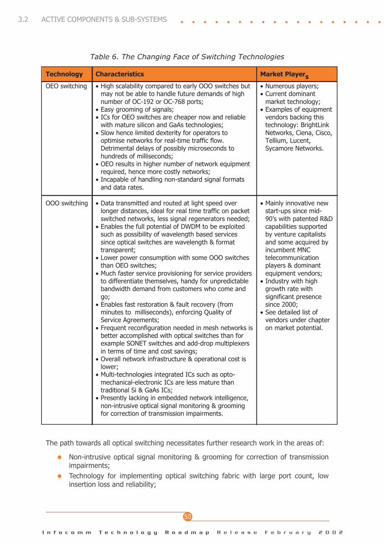
I n f o c o m m T e c h n o l o g y R o a d m a p R e l e a s e F e b r u a r y 2 0 0 2
50
Table 6. The Changing Face of Switching Technologies
The path towards all optical switching necessitates further research work in the areas of:
Non-intrusive optical signal monitoring & grooming for correction of transmission impairments;
Technology for implementing optical switching fabric with large port count, low insertion loss and reliability;
3.2 ACTIVE COMPONENTS & SUB-SYSTEMS
Technology Characteristics Market PlayersOEO switching • High scalability compared to early OOO switches but
may not be able to handle future demands of highnumber of OC-192 or OC-768 ports;
• Easy grooming of signals;• ICs for OEO switches are cheaper now and reliable
with mature silicon and GaAs technologies;• Slow hence limited dexterity for operators to
optimise networks for real-time traffic flow.Detrimental delays of possibly microseconds tohundreds of milliseconds;
• OEO results in higher number of network equipmentrequired, hence more costly networks;
• Incapable of handling non-standard signal formatsand data rates.
• Numerous players;• Current dominant
market technology;• Examples of equipment
vendors backing thistechnology: BrightLinkNetworks, Ciena, Cisco,Tellium, Lucent,Sycamore Networks.
OOO switching • Data transmitted and routed at light speed overlonger distances, ideal for real time traffic on packetswitched networks, less signal regenerators needed;
• Enables the full potential of DWDM to be exploitedsuch as possibility of wavelength based servicessince optical switches are wavelength & formattransparent;
• Lower power consumption with some OOO switchesthan OEO switches;
• Much faster service provisioning for service providersto differentiate themselves, handy for unpredictablebandwidth demand from customers who come andgo;
• Enables fast restoration & fault recovery (fromminutes to milliseconds), enforcing Quality ofService Agreements;
• Frequent reconfiguration needed in mesh networks isbetter accomplished with optical switches than forexample SONET switches and add-drop multiplexersin terms of time and cost savings;
• Overall network infrastructure & operational cost islower;
• Multi-technologies integrated ICs such as opto-mechanical-electronic ICs are less mature thantraditional Si & GaAs ICs;
• Presently lacking in embedded network intelligence,non-intrusive optical signal monitoring & groomingfor correction of transmission impairments.
• Mainly innovative newstart-ups since mid-90’s with patented R&Dcapabilities supportedby venture capitalistsand some acquired byincumbent MNCtelecommunicationplayers & dominantequipment vendors;
• Industry with highgrowth rate withsignificant presencesince 2000;
• See detailed list ofvendors under chapteron market potential.
I n f o c o m m T e c h n o l o g y R o a d m a p R e l e a s e F e b r u a r y 2 0 0 2
51
PH
OT
ON
ICS
EN
AB
LING
TE
CH
NO
LOG
IES
Optical buffering (memory) so that burst switching and optical packet switching can be implemented;
Large optical switching fabric with sub-nanosecond switching speed for optical packet switching.
Meanwhile, we expect OEO technology to continue to be in the mainstream optical switching market for the next few years. However, we also see the aggressive emergence of near all-optical switches providing cost efcient alternative to routing, reducing number of network components required and hence overall huge cost savings for networks among other advantages such as instant fault recovery and reconguration. At the same times, many vendors are also providing hybrid solution combining the advantages of both OEO and OOO technologies.
Today, most optical switching products such as those based on Micro-ElectroMechanical System (MEMS) are deployments in long-haul backbones. Over the next few years, we would see the gradual popularity of MEMS products entering metropolitan area network and possibly access networks in the longer term.
On the side of optical add-drop technology, we saw that the rst generation of OADMs were mainly inexible systems that can only access a xed set of predetermined wavelengths. The next generation of OADMs will encompass dynamic conguration and provisioning. This will allow the network to select any subset of wavelengths/channels to add and drop at a particular location. Dynamic conguration increases network exibility and response time, and it will allow service providers to provide bandwidth-on-demand services to clients.
The following describes the common technologies in optical switching or add-drop systems. This is followed by a comparison between them. Different applications would look for different performances offered by one or another of these technologies.
Micro-Electro Mechanical System (MEMS). MEMS is a surface technology that involves the micro-machining of existing silicon wafers to perform mechanical movements upon command by an electrical actuation voltage or in response to external environmental inputs such as acceleration, pressure or gravity, to achieve electrical or optical functions prevalent in modern day communication systems. MEMS micro-mirror switching is probably the most promising technology and we expect it to be the leading product in optical switching. In a MEMS optical switch, the micro-mirrors tilt back and forth, slide in and out, or pop up and down to reect or transmit optical signals;
Optomechanical switches or precision bulk optics. In this approach, light beams are shifted from one bre input to another bre output via mechanical alignments with possibly motor engines. It is a mature approach that gives robust connections, low loss and low cross talk. However, it is large, bulky, clumsy, slow and not cost effective;
Optoelectronic solid state waveguide switches. This is also a mature technology leveraging on solid state waveguide manufacturing processes combined with optical technology based on for instance Mach-Zehnder interferometers. The device material used in such switches can range from silicon, lithium niobate, indium phosphide, and barium titanate (early R&D stage). A signal’s passage into a waveguide is controlled by an electrical bias that creates a propagation delay by modifying the waveguide’s refractive index. This change in the speed of the light signal results in a change in its

I n f o c o m m T e c h n o l o g y R o a d m a p R e l e a s e F e b r u a r y 2 0 0 2
52
phase. Depending on the phase change, the signal is switched between two output ports. The main advantage of such switches is its extremely fast switching speeds in nanoseconds, a unique feature that allows this technology to maintain its foothold in research and commercial interest. It is also easily integrated with other solid state circuit functions. The disadvantages are polarisation dependent, high insertion loss, poor crosstalk performance for wideband channels, high operating voltages, and fairly costly. To have a signicant change in phase requires long travel paths, hence limiting the size of such switches to about 40 ports. Large size switches require the cascading of a series of smaller waveguide switches resulting in high signal loss. Hence, it is not scalable to large switch sizes;
Thermo-optical switches. Based on the same principle as the above, the speed of light in the waveguide is not changed by an electrical bias but by changing the temperature of the material that the light signal passes through. Materials such as polymer are often used;
Liquid crystal switches. This approach uses an electrical bias to modify the orientation of the crystal elements, which in turn affects the polarisation of light beam that is allowed to pass through or that will be reected. Two orthogonally splitted polarisations can be directed to two different output ports, hence perform a switching function;
Bubble switches based on total internal reection. This is a technology idea based on inkjet printing. When a light beam passes from one medium of higher refractive index into one of lower refractive index, above a critical angle of incidence, it can be totally reected. This change in refractive index can be brought about by introducing a uid (air or liquid) bubble at the junction of intersecting waveguides, hence reecting or switching light into the desired output waveguide or the absence of such a bubble can allow light to pass through unobstructed into another output waveguide;
Bragg grating switches based on holographic principles. In this approach, crystals are being laser etched with Bragg grating structures to create a hologram that reects changes in optical properties of the crystals when an electric eld is applied. Materials such as ferroelectric crystals in lithium niobate or potassium lithium tantalate niobate. Crystals are arranged in a matrix of rows and columns in a 2D manner corresponding to input and output ports. Insertion loss and crosstalk are main concerns.
3.2 ACTIVE COMPONENTS & SUB-SYSTEMS

I n f o c o m m T e c h n o l o g y R o a d m a p R e l e a s e F e b r u a r y 2 0 0 2
53
PH
OT
ON
ICS
EN
AB
LING
TE
CH
NO
LOG
IES
Tab
le 7. C
om
pariso
n b
etween
Optical S
witch
ing T
echnolo
gies
M
EM
SO
pto
-Mech
anical /
Precisio
n B
ulk
Op
tics
Op
to-electro
nic
So
lid S
tateS
witch
esLiq
uid
Crystal
To
tal Intern
alR
eflection
(e.g.
Bu
bb
le Sw
itch)
Ho
log
raph
icS
witch
es(e.g
. Brag
gG
rating
s)M
aturity oftechnology
•M
edium but m
aturefabrication processCM
OS com
patible
•M
ature•
Mature
•M
edium•
Medium
•M
ature
Scalability•
Limited w
ith 2DM
EMS to about
64x64 ports•
Higher scalability
with 3D
MEM
S tothousands of ports
•Very low
scalability•
Low, up to about
40 ports•
Low•
Low (to about 100
ports)•
Low
Switching
speed•
in microseconds
•in m
illiseconds(hundred’s)
•in nanoseconds
•in m
illiseconds(hundred’s)
•in m
illiseconds(ten’s)
•in nanoseconds
Other
technicalperform
ance
•Low
cross talk, lowinsertion loss,independent ofw
avelength/ bitrate/ polarisation &m
odulation formats
•Low
power
consumption
•Low
loss and crosstalk
•D
ependent onsignal polarisationas m
ost waveguide
devices•
High insertion loss
•Poor crosstalkperform
ance•
High pow
erconsum
ption
•M
ore suitable forsinglem
ode thanm
ultimode fibres
•Fairly low
loss, highisolation, low
erpow
er consumption
•Requires
polarisation splitter•
Suffers from PM
D,
moisture sensitivity
and thermal
fluctuations
•Trade off betw
eenlow
loss and highisolation required.
•W
avelength-dependent phaseshift caused bybubble and henceam
plitudedispersion in signaloutput
•H
igh power
consumption
•Low
power
consumption
•Polarisation andw
avelengthdependent, hencedispersion and loss
Robustness
& R
eliability•
Medium
•H
igh•
High
•H
igh•
High
•H
igh
Packaging•
Present newchallenges
•Lightw
eight
•Bulky
•Easily integratedw
ith solid state ICs
•Inconvenient butw
ith some recent
advancements
•Som
e degree ofprecision required
•Easily integratedw
ith otherfunctions such assignal equalisationand m
onitoring
Cost•
Low•
Costly•
Fairly costly•
Costly•
Low•
Low
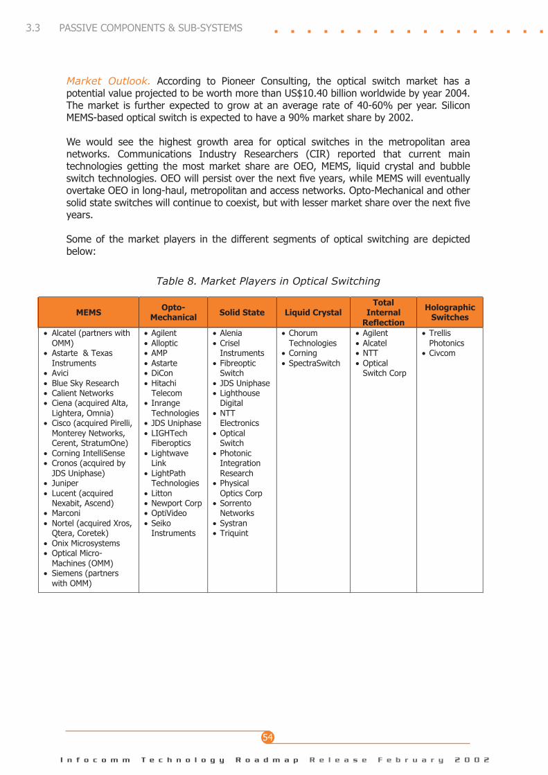
I n f o c o m m T e c h n o l o g y R o a d m a p R e l e a s e F e b r u a r y 2 0 0 2
54
Market Outlook. According to Pioneer Consulting, the optical switch market has a potential value projected to be worth more than US$10.40 billion worldwide by year 2004. The market is further expected to grow at an average rate of 40-60% per year. Silicon MEMS-based optical switch is expected to have a 90% market share by 2002.
We would see the highest growth area for optical switches in the metropolitan area networks. Communications Industry Researchers (CIR) reported that current main technologies getting the most market share are OEO, MEMS, liquid crystal and bubble switch technologies. OEO will persist over the next ve years, while MEMS will eventually overtake OEO in long-haul, metropolitan and access networks. Opto-Mechanical and other solid state switches will continue to coexist, but with lesser market share over the next ve years.
Some of the market players in the different segments of optical switching are depicted below:
Table 8. Market Players in Optical Switching
3.3 PASSIVE COMPONENTS & SUB-SYSTEMS
MEMSOpto-
Mechanical Solid State Liquid CrystalTotal
InternalReflection
HolographicSwitches
• Alcatel (partners withOMM)
• Astarte & TexasInstruments
• Avici• Blue Sky Research• Calient Networks• Ciena (acquired Alta,
Lightera, Omnia)• Cisco (acquired Pirelli,
Monterey Networks,Cerent, StratumOne)
• Corning IntelliSense• Cronos (acquired by
JDS Uniphase)• Juniper• Lucent (acquired
Nexabit, Ascend)• Marconi• Nortel (acquired Xros,
Qtera, Coretek)• Onix Microsystems• Optical Micro-
Machines (OMM)• Siemens (partners
with OMM)
• Agilent• Alloptic• AMP• Astarte• DiCon• Hitachi
Telecom• Inrange
Technologies• JDS Uniphase• LIGHTech
Fiberoptics• Lightwave
Link• LightPath
Technologies• Litton• Newport Corp• OptiVideo• Seiko
Instruments
• Alenia• Crisel
Instruments• Fibreoptic
Switch• JDS Uniphase• Lighthouse
Digital• NTT
Electronics• Optical
Switch• Photonic
IntegrationResearch
• PhysicalOptics Corp
• SorrentoNetworks
• Systran• Triquint
• ChorumTechnologies
• Corning• SpectraSwitch
• Agilent• Alcatel• NTT• Optical
Switch Corp
• TrellisPhotonics
• Civcom
I n f o c o m m T e c h n o l o g y R o a d m a p R e l e a s e F e b r u a r y 2 0 0 2
55
PH
OT
ON
ICS
EN
AB
LING
TE
CH
NO
LOG
IES
3.3 PASSIVE COMPONENTS & SUB-SYSTEMS
3.3.1 Connectors
I) Technology Overview
In optical communication systems and networks, one important task is to interconnect optical bres. This can be achieved using either splicing or connectors. Both fusing splicing and mechanical splicing are used currently. They provide very low loss permanent joint but are not very exible and need skilled labour to do it. Connectors provide a good alternative and are reasonably low loss. In the past, most of the telecommunication equipment manufacturers use FC connectors. Today, carriers use several types of connectors in different sections of their networks. SC, FC and ST connectors are still widely used. However, recently developed Small Form Factor (SFF) connectors have been widely used in switching hubs or with other transmission equipment where port density is critical.
II) Technology Developments, Issues & Challenges
Connectors are still evolving and are almost always application sensitive. As a general rule, the following applies:
SMA. This is the oldest type of connector and almost always used with 50 and 62.5um cable. This type of connector is mainly used for military equipment/applications;
ST. This is a twist-on connector and mainly used with multi-mode bre;
FC. This is the second generation twist-on connector and used with both single and multi-mode bre (62.5 and 9um);
SC. This is a snap-in connector used widely in data communication equipment for duplex transmission.
All connectors require great care in assembly and connection to prevent reections that create optical “kinks”, degrading performance. Connector quality is one of the most important factors affecting the performance of an optical transmission link. Good quality control is necessary. This normally requires the absence of any visible defect on the end face. Connector kits and polishing jigs are required for installation and test equipment, such as “Optical Time Domain Reectometer” (OTDR), used to measure kinks, reections and other cable anomalies to determine quality of the link.
SFF connectors have been developed in recent years. It uses 1.25mm ferrules instead of the 2.5mm ferrules used commonly in SC, FC and ST connectors. Its small form factor enables equipment manufacturers to build more ports into the same sized box. There are a number of SFF connectors that are widely used. These include LC, VF-45, MT-RJ and MU. Eventually probably one of these will emerge as the dominant one. Low loss and low cost will be key features to determine the winner. Development work is also ongoing to design new connectors with improved port density and lower cost.
Market Outlook. Bishop & Associates forecasted that worldwide connector shipments to the optical network equipment market amounted to US$650 million in 2000 of which US$81.3 million accounted for shipments to optical component manufacturers. By 2004, the global market for connectors to optical network equipment is projected to attain US$1.29 billion.
I n f o c o m m T e c h n o l o g y R o a d m a p R e l e a s e F e b r u a r y 2 0 0 2
56
SONET transport equipment in this forecast is the largest connector market for optical equipment, accounting for US$313.8 million in 2000. Digital cross-connect equipment represents the second largest category of connector consumption with factory shipments valued at US$87.2 million in 2000. Gigabit switch/routers are third in line with factory shipments valued at US$80.7 million in 2000. PON equipment is the fastest growing category of connector consumption.
3.3.2 Dispersion Compensators
I) Technology Overview
When data pulses transverse the bre, they are normally affected by chromatic dispersion (CD). This is due to the fact that optical signals at different wavelengths propagate at different speeds. At intervals along the bre, it is necessary to insert dispersion compensators to compensate for this dispersion. They are typically placed at the same location as optical ampliers. The impact of chromatic dispersion rises approximately as the square of the increase in data rate. At 10Gb/s every 70km of standard single mode bre (SMF) requires compensation. At 40Gb/s, this is reduced to 4.4km for SMF and about 19km for non-zero dispersion-shifted bre. In addition, the amount of dispersion at different wavelength is different. This is referred to as dispersion slope. As a result, dispersion compensators not only have to compensate for chromatic dispersion, but also the dispersion slope. Otherwise, one WDM channel may be compensated exactly, but other channels may be over or under compensated.
Another source of optical signal distortion is polarisation mode dispersion (PMD). It arises from the fact that all bres have a slightly elliptical cross-section and is therefore slightly birefringent. As a result the two polarisations of the optical signal will travel at different speeds. PMD changes with time since the magnitude of the birefringence changes slowly with time due to temperature effects. This is an additional problem especially for high-speed optical transmission system such as 40Gb/s system and above.
II) Technology Developments, Issues & Challenges
There are several techniques for minimising the chromatic dispersion problem. Amongst them, dispersion compensating bre (DCF) and chirped Fibre Bragg Gratings (FBGs) are the most widely used. DCF has high value of dispersion of the opposite sign as normal transmission bre. To compensate for the dispersion over an 80 km span of standard bre 12-16 km of DCF is typically used. However, DCF suffers from high level of attenuation and high level of non-linearity. These may affect the performance of a DWDM network. In addition, it is difcult to use it to compensate for dispersion slope which is dispersion different for different wavelengths. Chirped FBG is a popular alternative to DCF. Due to the chirping of the grating period, different wavelengths will be reected at different locations of the grating thus compensate for the difference in propagation delay introduced by the transmission optical bre. With proper design of the grating prole, it can also be used to compensate for dispersion slope which is one of the major problems in a high speed DWDM system. Current dispersion compensators used in systems are all xed. However, there is great need for these compensators to be tunable. This will enable system designers to have a better inventory management. They can use the same tunable compensator for different lengths and designs of optical bre. In addition, tunable compensators are also needed in recongurable
3.3 PASSIVE COMPONENTS & SUB-SYSTEMS
I n f o c o m m T e c h n o l o g y R o a d m a p R e l e a s e F e b r u a r y 2 0 0 2
57
PH
OT
ON
ICS
EN
AB
LING
TE
CH
NO
LOG
IES
optical networks as the optical signals in such networks propagate through variable length of optical bre. At high data rates, tunable compensators will also enable exact compensation of the dispersion.
Commercial tunable dispersion compensators are already available from a few vendors. A few approaches are used which include non-linear chirped FBG and compensator consists of two quadratically chirped FBG of opposite direction of chirp. The main concerns with FBG-based system are the tuning speed and delay ripple. Other possibilities include planar lightwave circuit (PLC), liquid crystal and virtually imaged phase array. Efforts are also given to design remotely adjustable (tunable) dispersion compensator module (DCM). Currently most carriers only require relatively low channel counts for live trafc. As such, the need for tunable compensators is not immediate. Current xed compensators system could satisfy market requirements. However, as we move toward higher channel counts and higher data rates (40Gb/s and above), there is a potential market opportunity for tunable dispersion compensator products.
PMD problem can be solved using two approaches. One approach is through better bre design. All new bres manufactured do not have any problem with PMD for up to 40Gb/s. Another approach is through PMD compensation. PMD is much more difcult to compensate since it is variable. A few possibilities are available. One is to use bre by moving the polarisation axis and setting the delay line. Another is to use micro-optic approach based on waveplates or fast opto-ceramic switches. Non-linearly chirped FBG, PLC and lithium niobate based approaches have also been demonstrated. A number of vendors have demonstrated PMD compensators, although the market size and the actual demand are still unknown.
3.3.3 Optical Filters
I) Technology Overview
Optical lter is probably one of the most important components in WDM optical communication systems and networks. It is used for WDM signal multiplexing and demultiplexing. It is also used for WDM channel monitoring, noise ltering and gain equalisation. A number of technologies are available for the implementation of an optical lter. Among them are: thin lm lter, reective grating, Fabry-Perot interferometer, FBG, arrayed waveguide grating (AWG), Mach-Zehnder interferometer and fused biconic coupler/lter. Tunable lters are also a disruptive technology that could enable low cost metropolitan deployment of WDM based networks. Other popular tunable technologies include tunable Fabry-Perot lter and tunable acousto-optic lter.
II) Technology Developments, Issues & Challenges
Thin lm lters and bre Bragg lters were among the earlier technologies whereas AWG lters are later developed to allow better manufacturing scalability.
Thin lm lter is probably the most widely used lter for DWDM optical communication system now. It uses many thin layers of dielectric materials, with alternating high and low index of refraction that give the lter its desired wavelength dependent reection and transmission characteristics. It has a good performance and high temperature stability. However, it is difcult to be used in WDM systems with high channel number due to increased insertion loss. In addition, it is limited to system with channel separation of

I n f o c o m m T e c h n o l o g y R o a d m a p R e l e a s e F e b r u a r y 2 0 0 2
58
100GHz and above, although using it together with interleaver enables it to be used in systems with much narrower channel spacing.
Fibre Bragg Grating lter is a wavelength selective, reective lter with a steep spectral prole. The optical bre is a stretchable medium. As one stretches the bre with the grating inside, the period size of the index perturbations and the effective refractive index will be changed which would induce a corresponding shift in the Bragg wavelength. This has the effect of changing the center wavelength of the lter. If the stretching is far below the elastic limit, this process is perfectly linear and recoverable. In fact, many grating manufacturers have used this effect to form the temperature compensation packaging for WDM and dispersion compensation. Tunable lters can also be made based on FBGs. The main challenge in making tunable lters out of FBGs is to achieve high speed (sub nanosecond) tuning for applications such as optical header recognition for all optical routing.
AWG lter uses an array of optical waveguides in which the lengths of adjacent waveguides differ by a xed amount, from one waveguide to the next. This variation results in a wavelength dependent diffraction pattern that is similar to the one from a plane grating. This diffraction pattern is then arranged so that different wavelengths illuminate different output bres. It is highly integratable and can be integrated with other component such as variable optical attenuators (VOA) or laser in WDM system with high channel count. The main drawback is the requirement for temperature control. However, recent developments in compensation techniques using polymer and athermal polymer AWG have partially solved the problem. FBG offers a low insertion loss and a good ltering characteristics. With athermal packaging FBG is also highly stable with temperature change. It enables a exible a number of add and drop channels when used in an add/drop multiplexer. The possibility of tuning over a wide range also allow it to be used in a number of other applications.
Filter technologies are also used in important applications such as for gain attening in optical ampliers, described as follows:
Gain attening application of lters for EDFAs. In recent years, gain attening lters have been proposed in several different technologies, these include fused tapered bre lter, acousto-optic tunable lter (AOTF), thin lm interference lter, FBG and twin core bre:
Fused tapered bre lters are made by heating and pulling certain segments of the bre and causing part of the core mode to become lossy cladding mode. The original bre diameter and strength is thus seriously compromised. For a complex multi-peak gain prole, it is difcult to maintain yield by heating and pulling various sections of the same bre. Most people used tapered bre lter only to remove the 1530nm peak. A related technology is to use twin core bre with wavelength dependent coupling between the two cores. However, this may still prove to be challenging;
AOTF can be effective in dynamically attening the gain to adapt to signal add-drops in the network. One disadvantage however remains with AOTF, due to the index difference between single mode bre and AOTF’s substrate material, lithium niobate, a typical
3.3 PASSIVE COMPONENTS & SUB-SYSTEMS
I n f o c o m m T e c h n o l o g y R o a d m a p R e l e a s e F e b r u a r y 2 0 0 2
59
PH
OT
ON
ICS
EN
AB
LING
TE
CH
NO
LOG
IES
device suffers very high insertion loss (in excess of 3 dB). This loss affects all channels and basically offset the gain in the ampliers. In addition, packaging such a device is a challenge and costly, the technology involved is similar to that of 2.5G to 10G modulators. Recently, bre based AOTF has been proposed and demonstrated. It has solved the problem associated with insertion loss, but reliability is still a concern;
Thin lm lters have high engineering costs of development and questionable high power handing ability;
For bre gratings, there have been several contenders: long period gratings, blazed gratings and standard short period gratings:
i) Long period gratings are periodic structures formed in the core of a photosensitive bre. Unlike their short period counterpart, the refractive index perturbations have a period size much larger, in the order of 200 to 400 microns. Long period gratings are extremely temperature sensitive and have fast decay characteristics. Commercial deployment has remained relatively limited;
ii) Blazed gratings consist of a tilted grating structure. The tilt angle is normally below 8º to 9º and has the function of coupling the core mode into various lossy cladding mode. While the advantage of blazed gratings is the absence of direct reection, making these can be a good challenge. As the tilt angle becomes large, other non-linear effects appear;
iii) Short period gratings seem to be most promising. They are passive, can be used in the transmission mode and can be tailored to atten the entire C-band of 35nm. Although there are some reections, most amplier designers will deploy an isolator into the amplier. This is to avoid reections from the splicing of other optical components: the pump signal WDM, SMF to Erbium-doped bre and monitoring tab couplers.
I n f o c o m m T e c h n o l o g y R o a d m a p R e l e a s e F e b r u a r y 2 0 0 2
60
3.3.4 Optical Fibres
I) Technology Overview
Optical bres can be Single Mode bres (SMFs) or Multimode bres (MMFs). Three major “windows” of wavelength are commonly used in conjunction with these bre types. The 850nm window is normally used with the MMF. 1310nm window is used for both types, while 1550nm window is used almost exclusively with SMF. This is the point of minimum attenuation in conventional optical bre (See Figure 17).
SMFs are distinguished from MMFs by their much thinner core diameter i.e. typically 8 to10 micron for SMF vs 50 to 62.5 micron for MMF. Due to their excellent low loss feature (as low as 0.2dB/km), SMFs are used mainly in long-haul transmissions at wavelengths of 1310nm and 1550nm. MMFs can carry hundreds of modes of light and are more common in short distance transmissions such as local area networks, for lower bandwidths ranging from 10MHz/km to 600MHz/km. They suffer from higher loss of 2 to 60dB/km and transmit typically in the range of 660 to 1060nm.
Figure 17. Typical Fibre Attenuation Characteristics
SMF solutions are often associated with higher costs than MMF solutions when we take into account the related connectors, splices, test equipment, transmitters and receivers. The alignment accuracy needs to be more stringent for SMFs and this greatly increases its assembly time compared to MMFs. In addition to these, other SMF designs are available with features that make them attractive for particular applications, such as undersea transmission.
The ITU today recognises four types of single-mode bres. Their characteristics and applications are briey summarised in the following table.
3.3 PASSIVE COMPONENTS & SUB-SYSTEMS

I n f o c o m m T e c h n o l o g y R o a d m a p R e l e a s e F e b r u a r y 2 0 0 2
61
PH
OT
ON
ICS
EN
AB
LING
TE
CH
NO
LOG
IES
Table 9. Characteristic of Optical Fibre Types
II) Technology Developments, Issues & Challenges
Today, optical bres are already developed into highly rened products. Yet leading manufacturers such as Corning, Alcatel and Lucent still actively pursue its development. Their aim is to develop lower loss and lower PMD bres that could potentially handle high-speed long distance DWDM transmission systems. Some key development trends of optical bre include:
Very wide bandwidth bre for higher transmission capacity;
Large effective core area bre for higher optical power while mitigating non-linear effects;
Type of Optical Fibre ITU Characteristics & Applications
Dispersion UnshiftedFibre (USF)
(sometimes calledstandard orconventional fibre)
G.652 • Most widely used fibre type;• Introduced commercially in 1983;• Zero chromatic dispersion at 1310nm;• High chromatic dispersion (approx. 17ps/nm-km) at 1550nm;
beyond 2.5Gb/s require the use of dispersion compensation forlong-haul;
• Used commonly for high-speed digital and CATV-type analogsystems operating in both the second and 3rd wavelengthwindows (see Figure 17).
Dispersion-Shifted Fibre(DSF)
G.653 • Commercially available since 1985;• Minimum chromatic dispersion wavelength adjusted to
1550nm, the region of minimum optical attenuation;• Non-linear effects is an issue;• Used for submarine systems, where a single wavelength is
transmitted over several thousands of kilometres. Some longdistance carriers have installed significant quantities of DSF interrestrial backbone routes;
• Can also be used in the 2nd window, but no commercialdemand due to high chromatic dispersion near 1310nm.
1550-nm Loss-Minimised Fibre
G.654 • A special type of USF with very low loss for the 1550nmwindow, typically <0.18dB/km;
• Using pure silica glass in the fibre’s core and deeply down-doping the fibre’s cladding, and maintaining a high cut-offwavelength;
• Difficult to fabricate, expensive and rarely used;• Use in non-repeatered submarine systems to enable
transmission over long distances without intervening activecomponents.
Nonzero-DispersionFibre
G.655 • Commercial production in 1993 by Lucent, called TrueWavefibre;
• Standardised by the TIA, ITU, and IEC;• Minimum (to suppress the four-wave mixing fibre non-linearity)
and maximum (to ensure chromatic dispersion is small for highchannel rates) amount of chromatic dispersion specified over aportion of the 3rd window;
• Used in the latest generation of amplified DWDM systemsextensively for both submarine and long distance terrestrialnetworks.
Figure 17)
I n f o c o m m T e c h n o l o g y R o a d m a p R e l e a s e F e b r u a r y 2 0 0 2
62
Multi-cladded bre for dispersion attened structures;
Dispersion compensating bre with lower loss and lower non-linearity;
Fibre with lower polarisation mode dispersion for ultra high speed transmission systems
The development of different types of optical network has created a need for the design of optical bre for different applications. For example, a bre with negative dispersion has recently been developed for the MANs market. This allows directly modulated laser to be used in the system since the dispersion created by the chirp of direct modulated laser can easily be compensated by the negative dispersion of the bre. This will enable great cost saving. Other developments have mainly been focusing on specialty bres, such as dispersion compensation bre, double cladding bre for high power bre laser, photosensitive bre for FBG writing and rare earth doped bre for amplication.
There are also plastic bres as the cheapest bre solution with good mechanical strength, but with high losses of 150 to 250dB/km and for low bandwidth application of 5MHz over 60m, as such, these are not really found in telecommunications due to poor performance. Plastic technology remains today more for R&D in the lab. Most optical bres for telecommunications use glass materials (silica). An intermediary between glass and plastics is plastic-clad silica that has a glass core with a plastic cladding. This type of bre experiences typical losses of 6 to 10dB/km, for bandwidth applications of up to 25MHz/km, and operates at wavelengths ranging from 660nm to 1060nm. However, it is difcult to connect such bres and they are also unstable.
An exciting new development in the area is photonic crystal bre or sometime called holey bre. It is an all silica optical bre with a hexagonal array of air holes typically sub-micron in diameter spaced apart by a few microns running along its length. Guiding cores are created in these two dimensional photonic crystal arrays by lling in or enlarging groups of one or more air holes. It possesses a number of unique and even extraordinary properties, permitting a much greater level of control of modal behaviour (effective index, single mode range, modal area and shape, group velocity dispersion) than is conceivable in conventional bre technology.
For example, photonic crystal bre (PCF) can be designed to be single mode at every wavelengths of excitation. This enables us to design single mode bres with zero dispersion at any arbitrary wavelength. It provides us with the possibility to design dispersion compensation bres for different operating wavelengths. At the same time, this offers the possibility of mode overlap for light of different wavelengths in the bre; this enables the improvement of non-linear interaction such as four wave mixing (FWM) greatly. The possibility of greater light intensity and loading holes with gases, low index liquids or non-linear polymers permits well controlled non-linear interactions over unlimited lengths of bre. All these give us the potential for implementation of all optical switching, FWM and Raman laser operation. Current research is still being carried out in the lab. However, it presents many challenges to be overcome, such as the need for precise alignment and joining of these bres. Nevertheless, work on optical bres and related equipment & machinery remains a possible R&D area for future efforts.
3.4 ADVANCED OPTICAL & MEMS PACKAGING AND AUTOMATED MANUFACTURING
I n f o c o m m T e c h n o l o g y R o a d m a p R e l e a s e F e b r u a r y 2 0 0 2
63
PH
OT
ON
ICS
EN
AB
LING
TE
CH
NO
LOG
IES
3.4 ADVANCED OPTICAL & MEMS PACKAGING AND AUTOMATED MANUFACTURING
I) Technology Overview
Advanced optical packaging techniques of opto-electronic, photonic and MEMS/MOEMS (Micro-Electro Mechanical System/Micro-OptoElectro Mechanical System) devices are perhaps the most important enabling technology to the optical industry, as it accounts for the majority of nal product cost. Opto-electronic devices handle both electronic and optical/photonic signals (e.g. optical transmitters and receivers), while photonic devices handle photons (e.g. light emitters, detectors, Bragg gratings). MEMS/MOEMS devices combine electronic, mechanical, optical signals (e.g. MEMS optical switch, MEMS optical add-drop multiplexers).
The packaging process exerts great inuence on the product’s manufacturing yield & quality, size and weight, electrical & optical performance, mechanical & thermal reliability, shock resistance, repeatability, maintainability, testability and can even contribute to environmentally friendly products with lead-free solders and halogen-free materials.
In review, the manufacturing industry at large has progressed from advanced electronic packaging (QFP, CSP, BGA, ne pitch ip chip, multi-chip packages, 3D vertical interconnects of 2 to 128 layers etc) to low cost, high density, compact, high power advanced RF packaging that could involve micro-machining, free space power combining techniques, multi-chip packages, 3D interconnects and photonic bandgap crystals for manipulation & processing of light. Much of the impetus for advanced RF packaging came from military programmes (such as major waves of funding from DARPA) with technology transfers to the commercial industry, but is also partly due to the advent of commercial wireless products.
The next lap would be to research and automate on optical packaging as we enter the age of next generation optical networks for the Internet, free space optics transmission, and many other commercial optical products in the areas of medicine, entertainment, displays etc. To achieve quantum leap performances, skills and new technologies need to be developed in the area of reliable packaging techniques that can seamlessly integrate complex multi-disciplinary expertise encompassing digital electronics (logic, memory etc), RF analogue, MEMS, optics and even nano-technologies to deliver world class system-on-chip products. In commercial optical modules such as optical detectors, transmitters, 40Gb/s optical modules, there is often a need to do co-design with microwave transitions and interconnects (e.g. differential pair signalling I/Os, microwave interconnects such as more advanced and increasingly popular coplanar waveguides). Co-design with thermal management such as with thermoelectric cooling modules in optical transmitters is also necessary. There are also critical skills needed in the areas of reliability and shock testing & analysis, assisted board and system level simulation & analysis, power plane analysis and modelling that are also playing a part to hasten the design process and to make robust products with good quality control.
The birth of DWDM technology has enabled terabits of information to be transferred through optical bre over thousands of kilometres. Optical networking component manufacturers are competing to churn out their latest products that boast of higher channel counts, higher modulation speeds and higher level of integration. Packaging of these components become even more challenging when optical devices and interconnects are being miniaturised.
Similar to electronics packaging, optical and opto-electronics packaging can be categorised
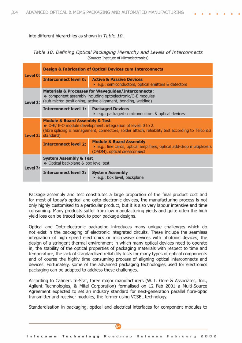
I n f o c o m m T e c h n o l o g y R o a d m a p R e l e a s e F e b r u a r y 2 0 0 2
64
into different hierarchies as shown in Table 10.
Table 10. Dening Optical Packaging Hierarchy and Levels of Interconnects(Source: Institute of Microelectronics)
Package assembly and test constitutes a large proportion of the nal product cost and for most of today’s optical and opto-electronic devices, the manufacturing process is not only highly customised to a particular product, but it is also very labour intensive and time consuming. Many products suffer from low manufacturing yields and quite often the high yield loss can be traced back to poor package designs.
Optical and Opto-electronic packaging introduces many unique challenges which do not exist in the packaging of electronic integrated circuits. These include the seamless integration of high speed electronics or microwave devices with photonic devices, the design of a stringent thermal environment in which many optical devices need to operate in, the stability of the optical properties of packaging materials with respect to time and temperature, the lack of standardised reliability tests for many types of optical components and of course the highly time consuming process of aligning optical interconnects and devices. Fortunately, some of the advanced packaging technologies used for electronics packaging can be adapted to address these challenges.
According to Cahners In-Stat, three major manufacturers (W. L. Gore & Associates, Inc., Agilent Technologies, & Mitel Corporation) formalised on 12 Feb 2001 a Multi-Source Agreement expected to set an industry standard for next-generation parallel bre-optic transmitter and receiver modules, the former using VCSEL technology.
Standardisation in packaging, optical and electrical interfaces for component modules to
3.4 ADVANCED OPTICAL & MEMS PACKAGING AND AUTOMATED MANUFACTURING
Design & Fabrication of Optical Devices cum Interconnects
Level 0:Interconnect level 0: Active & Passive Devices
4 e.g.: semiconductors, optical emitters & detectors
Materials & Processes for Waveguides/Interconnects :8 component assembly including optoelectronic/O-E modules(sub micron positioning, active alignment, bonding, welding)Level 1:
Interconnect level 1: Packaged Devices4 e.g.: packaged semiconductors & optical devices
Module & Board Assembly & Test8 O-E/ E-O module development, integration of levels 0 to 2.(fibre splicing & management, connectors, solder attach, reliability test according to Telcordiastandard)Level 2:
Interconnect level 2:Module & Board Assembly4 e.g.: line cards, optical amplifiers, optical add-drop multiplexers(OADM), optical crossconnects
System Assembly & Test8 Optical backplane & box level test
Level 3:Interconnect level 3: System Assembly
4 e.g.: box level, backplane

I n f o c o m m T e c h n o l o g y R o a d m a p R e l e a s e F e b r u a r y 2 0 0 2
65
PH
OT
ON
ICS
EN
AB
LING
TE
CH
NO
LOG
IES
enable multiple supplier sources to customers is still new to the advanced next generation optical market and denitely requires more effort and goodwill between the players in this industry. Similar effort for standardisation for Small-Form-Factor (SFF) bre-optic connector packaging has also been reported. We see however today only sporadic pockets of alliances for standardisation, for example in the US. New 40Gb/s systems and components could also benet from standardisation.
II) Technology Developments, Issues & Challenges
3.4.1 Optical-Electronic (OE) Integration
At this moment All Optical Networking seems to be a distant goal and some form of optical to electrical signal conversion (and vice versa) is necessary in the optical network, especially at the edge. At the package level, optical and electronic/microwave systems must be integrated in a seamless fashion for optimised performance. This typically involves the matching of characteristic impedance in passive interconnects, such as the microwave transmission lines leading to the photonic devices and the matching of velocities of microwave and optical waves in active interconnects such as electro-optic modulators.
As the transmission speed of networking components increases from a few gigabits to tens or even hundreds of gigabits, the package formats that can be used also diminish in choices. For example, for transceivers operating at OC-48 rates, TO-can packages are commonly seen and as the transmission rate increases to 10Gb/s at OC-192, buttery packages with differential line and coax terminals are used. For OC-768 rates of 40Gb/s and above, very expensive and low loss microwave coax connectors are currently more feasible for implementation.
The simulation and measurement techniques used by microwave package designers to characterise and optimise package interconnects can be applied to the design and development of opto-electronic packages. Discontinuities such as bends and transitions in the electrical path from the package connector, to the metal traces on the sub-mounts and optical device carriers should be modelled and optimised to achieve minimal signal loss. Full wave and quasi-static electromagnetic solvers are indispensable tools for the package designer to achieve this purpose. In addition, the solvers can also be used for the design of electrodes in the electro-optic modulators.
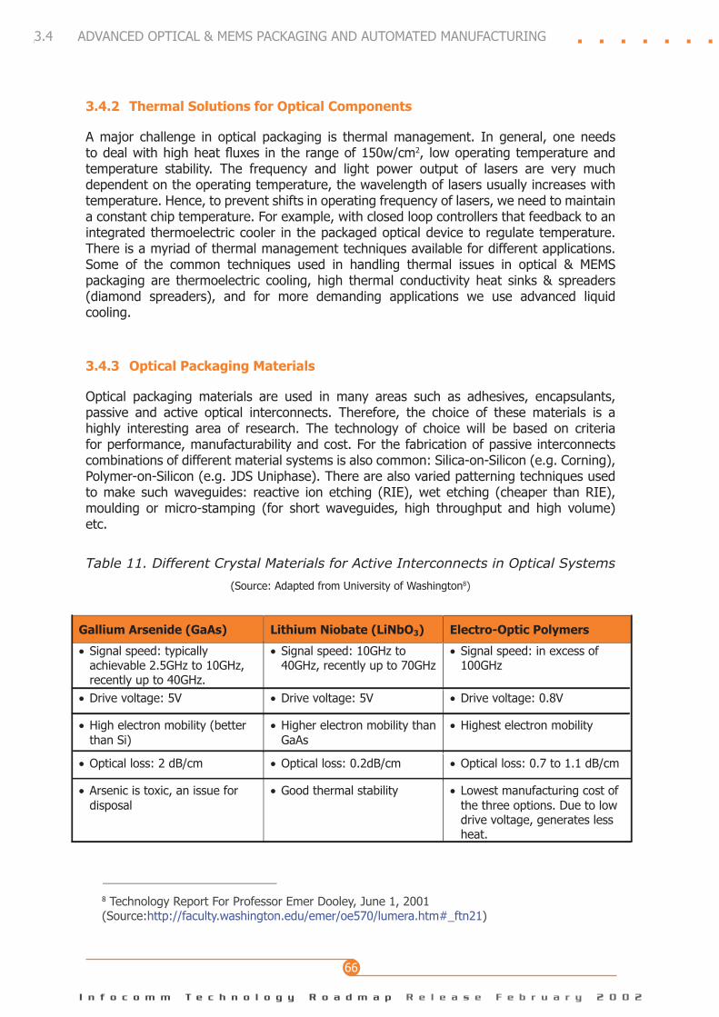
I n f o c o m m T e c h n o l o g y R o a d m a p R e l e a s e F e b r u a r y 2 0 0 2
66
3.4.2 Thermal Solutions for Optical Components
A major challenge in optical packaging is thermal management. In general, one needs to deal with high heat uxes in the range of 150w/cm2, low operating temperature and temperature stability. The frequency and light power output of lasers are very much dependent on the operating temperature, the wavelength of lasers usually increases with temperature. Hence, to prevent shifts in operating frequency of lasers, we need to maintain a constant chip temperature. For example, with closed loop controllers that feedback to an integrated thermoelectric cooler in the packaged optical device to regulate temperature. There is a myriad of thermal management techniques available for different applications. Some of the common techniques used in handling thermal issues in optical & MEMS packaging are thermoelectric cooling, high thermal conductivity heat sinks & spreaders (diamond spreaders), and for more demanding applications we use advanced liquid cooling.
3.4.3 Optical Packaging Materials
Optical packaging materials are used in many areas such as adhesives, encapsulants, passive and active optical interconnects. Therefore, the choice of these materials is a highly interesting area of research. The technology of choice will be based on criteria for performance, manufacturability and cost. For the fabrication of passive interconnects combinations of different material systems is also common: Silica-on-Silicon (e.g. Corning), Polymer-on-Silicon (e.g. JDS Uniphase). There are also varied patterning techniques used to make such waveguides: reactive ion etching (RIE), wet etching (cheaper than RIE), moulding or micro-stamping (for short waveguides, high throughput and high volume) etc.
Table 11. Different Crystal Materials for Active Interconnects in Optical Systems
(Source: Adapted from University of Washington8)
3.4 ADVANCED OPTICAL & MEMS PACKAGING AND AUTOMATED MANUFACTURING
8 Technology Report For Professor Emer Dooley, June 1, 2001(Source:http://faculty.washington.edu/emer/oe570/lumera.htm#_ftn21)
Gallium Arsenide (GaAs) Lithium Niobate (LiNbO3) Electro-Optic Polymers
• Signal speed: typicallyachievable 2.5GHz to 10GHz,recently up to 40GHz.
• Signal speed: 10GHz to40GHz, recently up to 70GHz
• Signal speed: in excess of100GHz
• Drive voltage: 5V • Drive voltage: 5V • Drive voltage: 0.8V
• High electron mobility (betterthan Si)
• Higher electron mobility thanGaAs
• Highest electron mobility
• Optical loss: 2 dB/cm • Optical loss: 0.2dB/cm • Optical loss: 0.7 to 1.1 dB/cm
• Arsenic is toxic, an issue fordisposal
• Good thermal stability • Lowest manufacturing cost ofthe three options. Due to lowdrive voltage, generates lessheat.

I n f o c o m m T e c h n o l o g y R o a d m a p R e l e a s e F e b r u a r y 2 0 0 2
67
PH
OT
ON
ICS
EN
AB
LING
TE
CH
NO
LOG
IES
The materials used for active interconnects can be classied into two groups: inorganic semiconductors (GaAs, LiNbO3) and electro-optic (EO) polymers as shown in Table 11. Inorganic materials incur higher manufacturing costs, have lower bandwidth, higher drive voltages, lower electron mobility than EO polymers. However, while EO polymers appear promising, they suffer from material defects arising from the difference in length of molecular chains that result in degradation and optical loss. Still, many have embarked on research in EO polymers also to partly help to reduce the cost of optical components.
3.4.4 Optical Assembly and Reliability Testing
The most challenging task in optical assembly is to launch the light in and out of the module. The critical and time consuming assembly steps are alignment and positioning of optical bres and components. In order to couple laser light with optical bre core, the assembly process requires sub-micron accuracy, ne resolution and high stability. The major requirements are to speed up production, increase the yield of assembly process and reduce the component cost. Optical ne precision assembly and bre handling are the principal cost drivers. The need of the hour is to automate manual processes, such as bre alignment, preparation and positioning.
The time required for optical assembly increases with the tolerances required and in turn, the cost of the module also adds up. In Figure 18, the typical optical assembly time increases when compared with the conventional surface mount and area array-ip chip assembly.
Figure 18. Optical Assembly Time Requirement vs Alignment Tolerance
(Source: OFC 2000, Paul O. Haugsjaa, Axiowave networks Inc.)
In packaging of bre optic components and modules the amount of signal loss that occurs across the component-to-component or component-to-bre junction is very critical. Extremely small size circular optical bre core (8-9µm in diameter), which is less than the width of a human hair, has to be aligned with a square, circular or elliptical light output from the device. Very high-resolution alignment system producing displacements in the nanometre range is capable of reducing the losses across the optical junction. However such high-resolution alignment system is costly at this moment. On the other hand, with small misalignment infant death of the product will happen. Misalignment of only one-tenth of a micron will result in a 30 percent loss of light coupling. The dedicated effort is the main
Single mode fibre Components
Multimode fibre Components
Flip Chip Mounting
Surface Mounting
Alignment Tolerance ( m )
Ass
emb
ly T
ime
(min
)
0.001
0.1
1
10
100
0.1 1 10 100 1000
I n f o c o m m T e c h n o l o g y R o a d m a p R e l e a s e F e b r u a r y 2 0 0 2
68
reason causing the packaging cost to be 30 to 60% of the total optical component cost, and hence becomes an area of key research to realise low cost and high efciency optical components and modules.
In electronic packaging, relatively small I/O count packaging such as TO & DIP were used initially. To achieve high density peripheral interconnects, packages such as TSOP and QFP, and then area-array interconnects such as WBGA and CSP, and nally advanced area-array interconnects such as ip chip BGA have come into existence over the last ten to fteen years. Today, active research is ongoing to achieve ner pitch ip chip technologies that will allow integration of even more I/O interconnects onto a single chip with better performances and shorter interconnects. In the area of optical assembly, advanced ne pitch optical BGA packages can allow low insertion loss and high performance for future applications in 10Gb/s and higher networks. To realise system integration in opto-electronics, future optical assembly has to leverage on various other ne pitch technologies such as wafer level processing, 3D packaging, surface activated bonding (SAB), new solder alternatives based interconnects such as Anisotropic or Isotropic Conductive Adhesive (ACA or ICA), gold-gold interconnects, diffusion bonding and micro-spring/coil/cantilever ip chip.
Like conventional electronic assemblies, optical assemblies also require undergoing of extensive reliability testing. New tests such as bre pull and bre torsion are required. In addition, the optical systems & their assemblies, unlike consumer electronics are expected to have much longer product life cycle. A more extended testing cycle is therefore required. At this moment, new standards and requirements for optical assemblies are being evolved by different standard bodies. The most common requirement, which the industry is following now, is the Telcordia general guidelines for optical assemblies.
3.4.5 MEMS Packaging Issues and Challenges
Optical MEMS are used in many applications including wavelength switching and power attenuation. The packaging of MEMS components with larger geometry size of >1um compared to traditional microelectronic packaging involves surface and bulk machining, 3D LIGA process for high aspect ration etching. MEMS packaging also has to take into account moving parts & structural reliability, hermetic sealing, thermal sensitivity, and its interaction with the environment, new quality check processes etc. In MEMS, there is also a lack of packaging databases and tools, with customised and internal development often required for its packaging. In optical mirror switches for example, precision alignment & attachment are required for the chip, bre and lens but each different mirror design requires different packaging considerations. V-grooves are sometimes used to place the bre and the bres held in place by a at glass cover. Assembled devices can be placed in a common package such as PGA package. Fibre coupling loss, sub mount attachment with minimal height variation, high frequency and high speed, moisture and temperature control, automated process for mass production are some of the challenges to overcome.
There is still no standard that exists in MEMS nor industry wide roadmaps available compared to traditional electronic packaging. Packaging of MEMS is driven by cost, performance, manufacturability and reliability. We can summarise the challenges in MEMS packaging via the following package categories as shown in Table 12.
3.4 ADVANCED OPTICAL & MEMS PACKAGING AND AUTOMATED MANUFACTURING
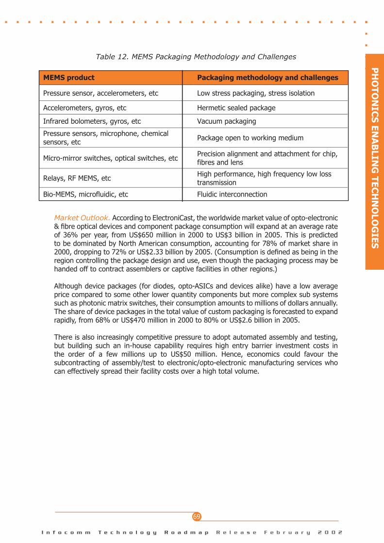
I n f o c o m m T e c h n o l o g y R o a d m a p R e l e a s e F e b r u a r y 2 0 0 2
69
PH
OT
ON
ICS
EN
AB
LING
TE
CH
NO
LOG
IES
Table 12. MEMS Packaging Methodology and Challenges
Market Outlook. According to ElectroniCast, the worldwide market value of opto-electronic & bre optical devices and component package consumption will expand at an average rate of 36% per year, from US$650 million in 2000 to US$3 billion in 2005. This is predicted to be dominated by North American consumption, accounting for 78% of market share in 2000, dropping to 72% or US$2.33 billion by 2005. (Consumption is dened as being in the region controlling the package design and use, even though the packaging process may be handed off to contract assemblers or captive facilities in other regions.)
Although device packages (for diodes, opto-ASICs and devices alike) have a low average price compared to some other lower quantity components but more complex sub systems such as photonic matrix switches, their consumption amounts to millions of dollars annually. The share of device packages in the total value of custom packaging is forecasted to expand rapidly, from 68% or US$470 million in 2000 to 80% or US$2.6 billion in 2005.
There is also increasingly competitive pressure to adopt automated assembly and testing, but building such an in-house capability requires high entry barrier investment costs in the order of a few millions up to US$50 million. Hence, economics could favour the subcontracting of assembly/test to electronic/opto-electronic manufacturing services who can effectively spread their facility costs over a high total volume.
MEMS product Packaging methodology and challenges
Pressure sensor, accelerometers, etc Low stress packaging, stress isolation
Accelerometers, gyros, etc Hermetic sealed package
Infrared bolometers, gyros, etc Vacuum packaging
Pressure sensors, microphone, chemicalsensors, etc Package open to working medium
Micro-mirror switches, optical switches, etcPrecision alignment and attachment for chip,fibres and lens
Relays, RF MEMS, etc High performance, high frequency low losstransmission
Bio-MEMS, microfluidic, etc Fluidic interconnection

I n f o c o m m T e c h n o l o g y R o a d m a p R e l e a s e F e b r u a r y 2 0 0 2
70
4.1 TELECOMMUNICATION INDUSTRY
I n f o c o m m T e c h n o l o g y R o a d m a p R e l e a s e F e b r u a r y 2 0 0 2
71
SIN
GA
PO
RE
LAN
DS
CA
PE
4 Singapore Landscape
4.1 TELECOMMUNICATION INDUSTRY
Despite the global economic downturn and the exit of several players, the telecom industry continues to see an increase in the number of Facilities-Based Operators (FBOs) and Services-Based Operators (SBOs). There are now over 30 FBOs and over 290 SBOs licens-ees as of Jan 2002. Among the players are global names such as MCI WorldCom, Reach International Telecom, and Global One Communications.
The projected capital investment from FBOs and SBOs for the next two to three years is estimated at S$2.64 billion. Of this, about S$1.2 billion will come from FBOs, while the remainder will originate from SBO licensees. The projected capital investment from FBOs over the next ve to six years is even higher, estimated at about S$1.8 billion.
In terms of international connectivity, Singapore has become one of the most connected cities in the world. Singapore has direct internet connections to over 30 countries with more than 45Mbps to key regional markets, US and Europe, making us one of the most connected business capitals around. Singapore has an extensive submarine cable network comprising of pan-Asian cables like APCN2, C2C, EAC, and Nava, among others. Singapore’s total cable capacity can be scaled up to 21Tb/s as of end 2001. Refer to Annex B for more information on these networks.
Singapore’s Internet Data Centers (IDCs) are also increasing in number. With 20 IDCs now in operation, content and service providers can choose from a wide range of competitively priced services. Some of the leading IDCs have regional and international points of presence and use Singapore as a gateway to the region. NTT Communications, for example, launched its S$23.5 million IDC in Singapore in Jul 2001. The center will be an integral part of NTT’s global IDC network.
High-speed data service such as GigaWave service is also available to customers that require massive bandwidth for their corporate data. This service is provided by SingTel since 2000. GigaWave is an optical network employing DWDM technology which supports transmission speeds of up to 2.5Gb/s, with speeds of 10Gb/s to be available soon. The almost unlimited amount of bandwidth capacity enables swift transmission of voice, data and video applications, without the need to install new bre cables.
Photonics and Optical Equipment Vendors
Singapore traditionally has a strong manufacturing base. One of the world’s leading contract manufacturer, Solectron, has recently chosen to locate its new Asia-Pacic headquarters here. It also enhances its manufacturing operations in Singapore to include the full-suite of manufacturing activities for high-end products, such as optical networking systems. Some of its main reasons for doing so are Singapore’s established strength in the electronics manufacturing business and her efcient logistics support systems. In addition, Venture Manufacturing, a major local contract manufacturer, is also manufacturing optical networking modules, and will continue to expand this part of its business.
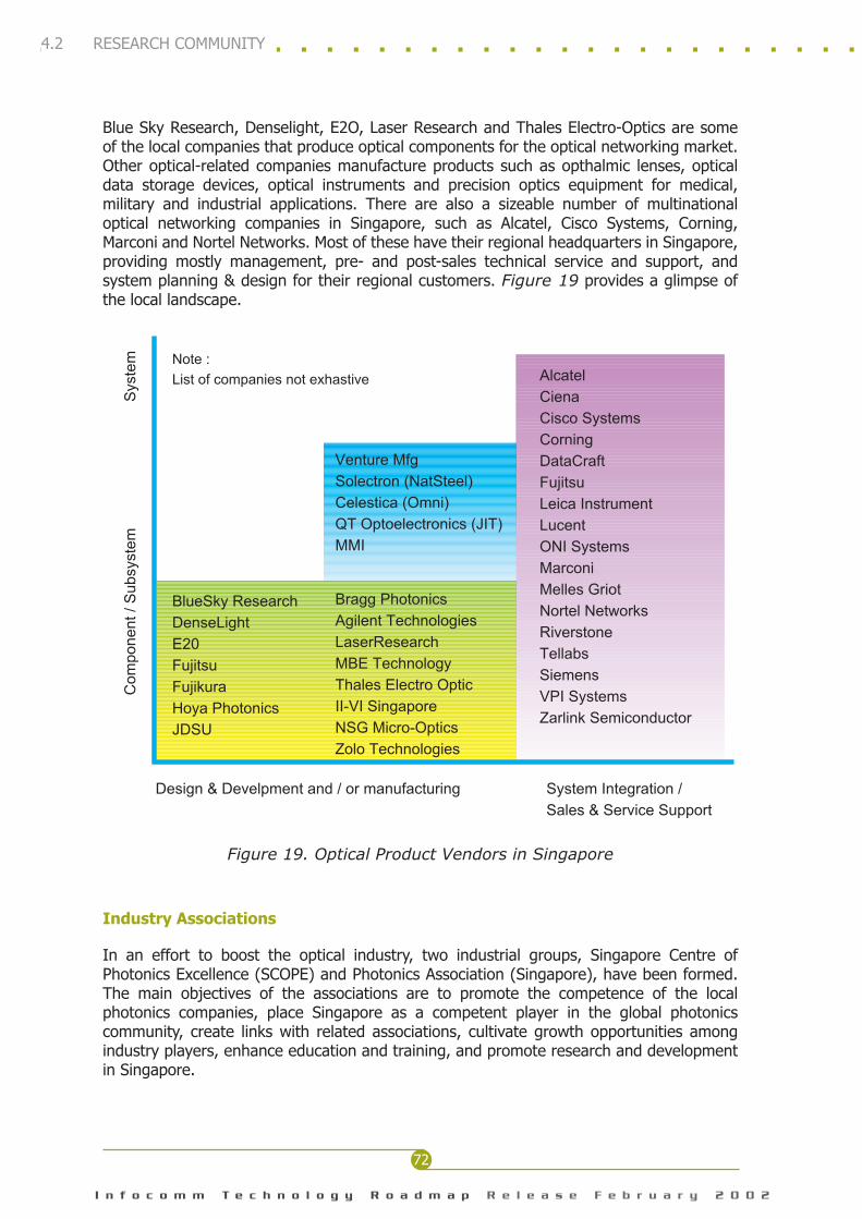
I n f o c o m m T e c h n o l o g y R o a d m a p R e l e a s e F e b r u a r y 2 0 0 2
72
Blue Sky Research, Denselight, E2O, Laser Research and Thales Electro-Optics are some of the local companies that produce optical components for the optical networking market. Other optical-related companies manufacture products such as opthalmic lenses, optical data storage devices, optical instruments and precision optics equipment for medical, military and industrial applications. There are also a sizeable number of multinational optical networking companies in Singapore, such as Alcatel, Cisco Systems, Corning, Marconi and Nortel Networks. Most of these have their regional headquarters in Singapore, providing mostly management, pre- and post-sales technical service and support, and system planning & design for their regional customers. Figure 19 provides a glimpse of the local landscape.
Figure 19. Optical Product Vendors in Singapore
Industry Associations
In an effort to boost the optical industry, two industrial groups, Singapore Centre of Photonics Excellence (SCOPE) and Photonics Association (Singapore), have been formed. The main objectives of the associations are to promote the competence of the local photonics companies, place Singapore as a competent player in the global photonics community, create links with related associations, cultivate growth opportunities among industry players, enhance education and training, and promote research and development in Singapore.
4.2 RESEARCH COMMUNITY
I n f o c o m m T e c h n o l o g y R o a d m a p R e l e a s e F e b r u a r y 2 0 0 2
73
SIN
GA
PO
RE
LAN
DS
CA
PE
Singapore Centre of Photonics Excellence, SCOPE (http://www.scope.org.sg) is set up by nine agencies related to the optics technology development in Singapore, namely the EDB, A*STAR (formally NSTB), PSB, NTU, NUS, DSI, IMRE, IME and Gintic. It is a platform to showcase and provide access to the competencies and R&D resources in Singapore. It aims to harness all the brains in the eld of optics/photonics currently residing in the various research institutes and universities in Singapore. It serves as a platform to generate relevant projects among enterprises, and to train and develop manpower to help nurture this industry in Singapore.
Photonics Association (Singapore), PA(S) (http://www.singoptics.org) is an industrial group set up to promote synergy, education and enhancement activities in the photonics industry in Singapore. It has a much wider range of companies, including precision engineering and optics manufacturing, and are more industry focus.
4.2 RESEARCH COMMUNITY
Presently, there are various photonics research work in the two universities and various research centres in Singapore. Most research work is done at the optical device level, with system level research mostly performed at the NTRC.
The Network Technology Research Centre (NTRC) in NTU conduct long-term research in optical networking and photonics research. Amongst the technologies investigated by NTRC are some state-of-the-art research in soliton transmission and Raman optical ampliers. NTRC has developed the mode locked ring bre laser that can act as a source with very high speed and ultra-narrow soliton pulse. It has also developed an all-optical gain-clamping Raman bre amplier to realise the amplication for both C-band and L-band signal. The centre’s work on a unique laser splicing technique has attracted much attention from the scientic and engineering communities. NTRC has also led 2 patents on bre Bragg grating technology and one patent on optical MEMS switch for implementing all-optical network and lowering the cost of communication systems.
Collaborating actively with industry partners in the development and transfer of leading-edge technologies, KRDL spearheads the research and development of information and networking technology. In the area of next generation network, KRDL has worked on policy-based network and bandwidth allocation for broadband network. SPRINGi is Singapore’s rst Resilient Packet Ring (RPR) testbed facility implemented by KRDL. It is funded by NSTB, with dark bre partly sponsored by Singapore Telecom. The RPR technologies evaluated was based on Cisco’s Dynamic Packet Transport.
In the area of optical packaging, the Institute of Microelectronics (IME) focuses more on electro-optical-wireless packaging with core competencies established in design, simulation, analysis, material characterisation, assembly, reliability assessment/modelling and failure analysis. Some of the joint projects with the industry have led to the creation of novel patents and cost savings in fabrication & packaging. In the area of MEMS, IME has developed a unique set of capabilities in a total solution for MEMS from concept to manufacturing – what IME called “One stop shop for MEMS products” encompassing design of MEMS devices and their ASICs, fabrication, packaging and testing.

I n f o c o m m T e c h n o l o g y R o a d m a p R e l e a s e F e b r u a r y 2 0 0 2
74
The Joining Technology Group (JTG) in Gintic has also started investigation on packaging of photonic components since 2001. A bonding workstation specically designed for optic packaging is under development, which will integrate functions of bre alignment/attachment, epoxy dispensing/curing and process monitoring. Photonic testing and reliability evaluation systems are being established, which are to enable the performance characterisation according to Telcordia requirements. The photonic components which are under investigation include 980nm laser diode and MEMS-based bre optic switch. Apart from the activities on optical packaging, JTG is developing some new MEMS-based photonic components. One of the examples is a micro-optic switch under the collaboration with Institute of Microtechnology (IMT), University of Neuchatel, Switzerland, and National University of Singapore (NUS). Thus far, a 1x4 type of MEMS optic switch has been successfully developed and under component-level packaging in JTG. The design of a scalable (NxN) type of MEMS optic switch has been put forward and the fabrication has been scheduled within 2002.
The Institute of Materials Research and Engineering’s (IMRE) competency with advanced device processing technologies and novel device structures is critical to making full use of the electrical and optical properties of III-V compound semiconductor materials and to developing new devices with better performance. Several technologies have been developed for producing semiconductor lasers for optical bre communication applications: a method of fabricating quantum wire structures and device structures with quantum wires, novel device structures for high temperature semiconductor lasers, and semiconductor material band gap tuning technologies for tunable and multiple wavelength semiconductor lasers.
Annex C provides more information of the research institutions/centres in Singapore.
4.3 GOVERNMENT AGENCIES
The way ahead for infocomm technology development is to harness the cross cluster industrial and research capabilities, as well as multi-domain expertise of government agencies. This is even more so in the age of technology convergence, not only within the infocomm sector itself, but also with other non infocomm sectors such as life sciences, nanotechnologies, mechanics, precision engineering and manufacturing etc. It is not only about bringing IT to the non-IT sectors for the benet of the economy, but is also about bringing non-IT sector expertise to help grow the IT sector in return. For instance, high-end optical networking products currently lack the competency in automated precision engineering and manufacturing, and some critical tasks are still being done manually. To help grow this IT sector, we need to co-develop the manufacturing base to high-end precision automation. To achieve this end, there is still ample scope for R&D in such high end manufacturing process and automation. These requirements and others have pooled together government agencies mainly A*STAR and EDB to closely collaborate to develop the optical networking and photonics community in Singapore. Below are some information on these agencies and a few examples of past project collaborations.
Agency for Science, Technology And Research, A*STAR (http://www.a-star.gov.sg) One of the key focus of A*STAR is to strengthen the scientic knowledge and economic competitiveness of Singapore in order to develop a foundation of high quality research
4.3 GOVERNMENT AGENCIES

I n f o c o m m T e c h n o l o g y R o a d m a p R e l e a s e F e b r u a r y 2 0 0 2
75
SIN
GA
PO
RE
LAN
DS
CA
PE
here. Over the years, it has funded numerous optical-related projects i.e. IP over WDM network9, SINGAREN 2110, MEMS11, etc A*STAR also aims to promote the exploitation of intellectual property created by our RICs, nurturing talent to advance Singapore’s transition to a knowledge-based economy.
In its continual effort to develop photonics research capabilities in Singapore, an Optical Network Focused Interest Group (ONFIG) was formed in April 2001 to work on strategic areas related to optical access technology, by pulling together competencies in photonics, electronics and software. The ONFIG members include the various RICs such as DSI, IME, IMRE, ICR, LIT, NUS-EE, NTU-µE (photonics group) and Gintic with over 150 researchers participating in the projects. The ONFIG team has proposed projects covering the software aspect of network, protocol and system architecture, and the component area of optical/electronic components and subsystems. Six projects were started on 1st Dec 2001 and scheduled to run for two years. A*STAR hopes that this will create greater synergy and collaboration among these organisations in order to position Singapore research capabilities in a better position with the advanced nations.
EDB (http://www.sedb.com/edbcorp) The Singapore Economic Development Board (EDB) aims to develop Singapore into a leading optical networking hub for Asia, enabling the broadband revolution by providing solutions in R&D, manufacturing and technical services. EDB intends to build up a optical networking ecosystem in Singapore, building a synergistic critical mass of companies covering each level of the value chain, bringing together carriers, systems integrators and discrete device manufacturers.
To achieve this, the EDB would be developing critical supporting infrastructure necessary to these players. EDB is currently working actively with local industry, leveraging on their experiences from the mature precision engineering cluster and semiconductor industries to develop the necessary packaging capabilities and build up a pool of packaging and automation solution providers to meet the performance and cost requirements of today’s device manufacturers. EDB will also continue to enhance its manufacturing value proposition to optical systems companies, through engaging more optical manufacturing services players to use Singapore as a manufacturing hub, leveraging on the Singapore-Riau islands strategy.
Leveraging on a strong R&D community with multidisciplinary capabilities, EDB also seeks to establish Centres of Competencies (CoCs) in optical networking - to embark on incubation, development and test-bedding of new technologies. One of the key to attracting such a thriving community is One-north, an exciting S$15 billion development of vision and inspiration where ideas grow, where innovators in biomedical sciences, infocomm technology (particularly optical and wireless networking, and pervasive computing) and media work, live, play and learn in a 200 hectares environment located at Buona Vista, Singapore.
9 Co-fund with MOE to develop a high-speed parallel optical packet routing technique to alleviate the electronic bottleneck of IP routing over WDM network.10 Funded NTRC on a second phase of SingAREN on multiprotocol lambda switching (MPlS), which aims to develop the core software and rmware to control OADMs and OXCs.11 Funded NTU Photonic Group for the optical MEMS project.

I n f o c o m m T e c h n o l o g y R o a d m a p R e l e a s e F e b r u a r y 2 0 0 2
76
At the same time, the EDB will develop an optical knowledge-based workforce through proactively investing in building capabilities. It has developed various manpower training programmes in photonics-related disciplines at various levels for both professionals and technicians. On-going EDB programmes in this area include the Specialist Manpower Programme (SMP), Overseas Training & Attachment Programme (TAP), Research & Training Programme (RTP) and Post-graduate Manpower training Programme (PMP). Through the training programmes, EDB partners with the industry to provide skilled manpower fuelling the growth of companies in Singapore (More information on EDB’s training schemes can be obtained from EDB’s website).
Through creating such an ecosystem, the optical networking industry can benet from the positive spin-offs generated from cross-cluster linkages and achieve long term progressive growth, riding on arbitrage opportunities made possible by the Free-Trade agreements and bilateral relations Singapore has with many of the world’s major markets.
IDA (http://www.ida.gov.sg) The Infocomm Development Authority of Singapore (IDA) was formed on 1 December 1999 from the merger of the Telecommunications Authority of Singapore (TAS) and the National Computer Board (NCB). Infocomm 21 is IDA’s blueprint for harnessing information communication technologies for national competitiveness and improving the quality of life of Singaporeans. The blueprint articulates the vision, goal and strategies that would facilitate the development of our infocomm industry over the next ve years, and move Singapore into the ranks of ‘rst world economies’ of the Net age.
In collaboration with the industry, research centres and other government agencies such as EDB and A*STAR, IDA has developed this technology roadmap on Next Generation Optical Network and Photonics. The roadmap initiative that begins with this technology report will call for the stakeholders to come forward to co-develop strategic technologies in this area and to elevate Singapore to become a world class infocomm technology hub.
IDA facilitates projects with positive impacts to the direct development of the local infocomm industry. In 1999, NTRC was funded for the building of a next generation optical network test-bed. The Singapore Advanced Research and Education Network (SingAREN) was set up with A*STAR to better in-country optical network research. Another project, Development of WDM Devices, Equipment and Test-bed was to develop several key technologies for implementing DWDM network.
4.3 GOVERNMENT AGENCIES

I n f o c o m m T e c h n o l o g y R o a d m a p R e l e a s e F e b r u a r y 2 0 0 2
77
SIN
GA
PO
RE
LAN
DS
CA
PE

I n f o c o m m T e c h n o l o g y R o a d m a p R e l e a s e F e b r u a r y 2 0 0 2
78
5 CONCLUSION
I n f o c o m m T e c h n o l o g y R o a d m a p R e l e a s e F e b r u a r y 2 0 0 2
79
CO
NC
LUS
ION
5 Conclusion
Optical Networks. Next generation optical networks will support IP trafc efciently over a WDM optical transport network with quality of service (QoS) provisioning, and an optical control plane that will allow wavelength routing, network restoration and survivability functions to be implemented at the optical level. This will achieve more functionality, higher transparency, higher exibility and an improved internetworking capability.
For long-haul network, innovations and technology breakthroughs in DWDM will bring about bigger pipes for the internet backbone. The technologies in this space are more mature and stable, and the market is established and relatively well understood.
In the metropolitan space, we see the budding of competitive as well as complementary technologies serving varied needs and a great potential for industry growth. Many of these new technologies are not as mature and we are seeing several exciting innovations in this space such as Resilient Packet Ring (RPR) and 10-Gigabit Ethernet (10GbE) technologies. As the metropolitan marketplace is not well established and cluttered with many new and legacy technologies, this sometimes results in a confusing landscape.
As for optical access network, we see that the market will need more time to develop. This is mainly because of the high cost of Passive Optical Networks (PONs) deployment, and the availability of many viable last mile solutions such as xDSL, HFC and free space optics.
Standards. Networking and telecommunication standards development has traditionally been a good indicator of the expected development path of technology and its adoption. A good number of standards covering framework, physical layer aspects, interfaces, functional characteristics have been completed by ITU-T. There are many more in the pipeline, such as distributed connection management, routing and discovery, and OTN link management. Optical networking standardisation also see close co-operation between traditionally carrier and voice-centric ITU and data/IP centric IETF in working towards an automatic switched transport network. The development of Digital Wrapper, ASTN/ASON and the unied optical control plane will have major impact on the operation of future optical carrier network.
Photonics. Today, the state-of-the-art photonic systems are lled with technological breakthroughs in many areas. We have identied the following important technologies that have ample scope for future development. These technologies are summarised below:
DWDM technology remains to be important. The major development efforts are to achieve closer channel spacing, higher data rate per wavelength, wider optical bandwidth and higher spectral efciency. Alternative technologies such as CWDM will still be used and developed further for cost sensitive areas such as data communication and optical access networks. OTDM can be used together with DWDM to further increase network capacity but its implementation may still be many years away;
There are strong interests in the deployment of 40Gb/s system. Components for the system need to be developed which include high-speed modulators, high-speed detectors and high-speed receivers. Other components such as CD and PMD compensators are also needed;
I n f o c o m m T e c h n o l o g y R o a d m a p R e l e a s e F e b r u a r y 2 0 0 2
80
EDFAs & TDFAs are being developed further so that S-band, C-band and L-band can be fully utilised. Raman ampliers and other amplier technologies are also being developed so that other bands can also be used. Technologies such as EDWA, SOA and low cost uncooled pump laser are being studied so that low cost ampliers for metro network can be developed;
Tunable components are very important for optical network development. Wideband tunable lasers, tunable lters and tunable compensators are being studied actively. Various technologies are being pursued to achieve high tuning speed and wide tuning range. Components with sub-nanosecond tuning speed may also be important for future optical burst and packet switching networks;
Technologies that can lower system cost such as VCSELs for 1310nm/1550nm devices, Very Short Reach (VSR) optical interconnects and small form factor connectors have attracted much attention;
Future technologies such as optical 3R, soliton and photonic crystal bre may greatly improve network performance;
A number of optical network related issues have been discussed in the report:
R&D technologies to enable automated, less costly, higher performance, high yield packaging, precision alignment, assembly and testing of optical and MEMS devices, components and subsystems;
R&D in packaging technologies: O/E compact reliable integration, cost effective and stable thermal management solutions, choice of suitable materials for low loss/high power/high speed/thermally stable photonic components, patterning techniques for making waveguides.
We summarise our views as follow:
There is a need for standardisation in photonic components and subsystems, including their interfaces and assemblies. For optical interconnects and assemblies, these could include inter-chip, inter-board and inter-shelf optical connectors, backplane interfaces, and line card interfaces, splices and very short reach optic cables. There is also a need to standardise reliability tests for optical components;
The photonic community should continue to monitor, participate and be consistent with international standards on optical network architectures and unied control plane to allow multi-vendors interoperability;
Automation is a vital step towards high volume and low cost manufacturing. To achieve this, there is a need to support highly automated optical manufacturing and processes;
5 CONCLUSION

I n f o c o m m T e c h n o l o g y R o a d m a p R e l e a s e F e b r u a r y 2 0 0 2
81
CO
NC
LUS
ION
Assembly and component packaging have also been identied as a key area for development, and potential commercial advantage. There should be more collaboration efforts in this area among the photonic community;
Integration of optics and electronics is critical to drive future photonic products into smaller packages, which ultimately result in small system footprint. High levels of functionality and complete solutions offering could be achieved by integrating monolithic, hybrid and discrete components into modules and subsystems. Such components include lasers, modulators, splitters, receivers/detectors and multiplexers;
Test-bedding facilities, qualication and certication are vital to the design and development of photonic components and systems. Hence, the close proximity and availability of such facilities would facilitate product development and commercialisation;
Regular networking activities and seminars organised by associations such as SCOPE and PAS are useful both for researchers and the industry in this sector, as well as for the setting of businesses in Singapore and abroad.

I n f o c o m m T e c h n o l o g y R o a d m a p R e l e a s e F e b r u a r y 2 0 0 2
82
ANNEX A

I n f o c o m m T e c h n o l o g y R o a d m a p R e l e a s e F e b r u a r y 2 0 0 2
83
Annex A. Optical Networking in Other Countries
This section surveys the industry and academic research development globally and in the region. Focus is placed in, Canada, Europe (on UK & Germany), China, Japan, Korea and USA as there are extensive activities and developments in these countries.
Photonics is internationally recognised as a key enabling technology. As far back as 1996, photonics was identied as a “critical technology” in the US National Critical Technologies list. Japan’s Ministry of International Trade and Industry (MITI) has identied photonics as an essential technology, and the government of Taiwan has specied photonics as a key discipline to target for development. China, to meet the challenges especially upon acceding to WTO, has listed the photonics technologies to be the newest resource of economic development and the most important technologies to develop in the new century. The German Fraunhofer Institute has identied photonics as an area undergoing rapid development, with innovations increasingly coming to the market.
In the following sections, we will give a brief overview of the development in their respective domestic market in terms of size and share of optical communication. Funding and investment by government and private investors are also provided. We also summarise a few industry and academic research initiatives.
A.1 CANADA
The photonics sector generated about US$5.75 billion in 2000 and forecasted to grow to US$11.5 billion by 2003 (Industry Canada). Québec holds about 40% of the Canadian photonics market, which represented more than US$2.5 billion in 2000. Photonics clusters were already well established with many of the world-leading companies populating the Québec City - Montréal - Ottawa corridor.
Canada has an impressively large number of SMEs in the eld of photonics, many of which are spin-offs from established organisations, either from large companies or research establishments, or start-ups of personnel from these organisations. These smaller rms and research intensive start-ups offer considerable growth potential by creating their own niche in photonics technologies. System level integration is available through Nortel Networks and Alcatel; these large companies provide resources that are not available to most individual researchers. Large component manufacturer such as JDS Uniphase usually maintains a portfolio of technologies, products and intellectual property to allow them the exibility to choose the most appropriate technology for any given customer. Going forward, many Canadian companies view automation and packaging technologies as a vital area of development, both to reduce costs, and to meet volume production.
A signicant amount of research funding from the government is allocated to the investigation of photonics technologies for optical communications, funding networks development through industry-driven consortia. One notable network in Canada is CANARIE. The CANARIE National Optical Internet initiative, called Ca*Net was in fact the world largest high-speed ATM network back in 1994. Ca*Net was eventually upgraded to Ca*Net II in 1997. Ca*Net II operates on top of ATM and SONET, which then rides over DWDM. Taking the technology a step further, Ca*Net 3, an IP-based WDM network, is planned for speeds of at least 40Gb/s. Ca*Net 3 network is designed to run directly over DWDM, significantly increasing its speed and
AN
NE
X A
I n f o c o m m T e c h n o l o g y R o a d m a p R e l e a s e F e b r u a r y 2 0 0 2
84
efciency. This provides Canada with the fastest research network in the world.
A.2 CHINA
According to RHK, China’s optical transport market reached US$1.1 billion in the rst half of 2001 and expected to achieve US$1.9 billion for 2001. Factors driving this market are deregulation, rising xed line and mobile voice penetration, and emerging interest in data services. China’s optical transport market is projected to reach US$5.5 billion by 2004. In market share, RHK nds that Huawei’s leadership in the overall optical transport market was the result of its strong position in the SDH segment. SDH is still the largest market segment in China, and Huawei dominants the more price-sensitive provincial and local markets. Following Huawei in the SDH market is ZTE, Nortel, Lucent, Marconi, Alcatel, Siemens and newcomer.
The major thrust in optoelectronics manufacturing today is cost reduction. Many companies are looking to China for low-cost manufacturing solutions. While the electronics industry is experiencing a worldwide downturn, China has potential as the bright spot for optoelectronics manufacturing. The Chinese government has recently set up six photonic valleys throughout China hoping at least one of them will blossom into something like the Silicon Valley of US. These valleys are mainly located at Beijing, Changchun, Shenzhen, Shijiazhuang and Wuhan. Among them, Wuhan and Shenzhen are the two largest production bases for optical products.
In China, associations such as the Chinese Optical Society (COS), China Optics and Optoelectronics Manufacturers Association (COEMA) and Photonics Society of Chinese-Americans are actively supporting the photonics industry. Several national laboratories have been established and linked to the universities, institutes or the industry. China has also constructed important government-hold Integrated Optics and Photonic Lab and Optoelectronics Technology & Engineering Centres. Its aim is of course, to spur universities, research institutes and the local governments to collaborate to promote technical transfers of knowledge, joint R&D projects and establishment of hi-tech start-up companies.
A.3 EUROPE
The photonics industry has also generated considerable interest in R&D and industry developments in Europe. Although there are signs of individual efforts in various European countries to develop this industry, there are also signicant joint European R&D efforts. According to RHK, the market for European optical transport, including SDH, DCS and WDM equipment will reach US$9 billion in 2001, reaching US$14.8 billion by 2004.
In Europe, many projects on optical networking were experimented. A more outstanding one is the Advanced Communications Technology and Services, called ACTS programme. ACTS purpose is to accelerate the deployment of advanced communications infrastructures and services, and is complemented by extensive European research in the related elds of information technology and telematics. Photonic technology and infrastructure concepts developed in ACTS will be validated in trials at many locations throughout Europe.
United Kingdom (UK). UK has a particularly strong presence of some of the world leading optical communication systems companies such as Alcatel, Marconi Communications and Nortel Networks. The Department of Trade and Industry (DTI) estimates that total
ANNEX A
I n f o c o m m T e c h n o l o g y R o a d m a p R e l e a s e F e b r u a r y 2 0 0 2
85
UK production of photonics systems and components for 2000 was around £4 billion, accounting for half of total EU production. These companies have manufacturing bases in UK. Other leading US companies such as Cisco, Corning and Lucent have also established design and optical network development centres near London. UK has also a strong R&D and manufacturing base for bre-optic components such as laser diodes, transceivers and ampliers. Global players in the UK include Agilent Technologies and JDS Uniphase. UK is also a large producer of optical bre and cable and the main producers are Corning and Pirelli.
The UK has substantial academic strengths in optoelectronics and photonics technologies, stimulated by programmes funded by the Engineering and Physical Sciences Research Council (EPSRC), DTI and other Government bodies. As part of the Government’s LINK initiative, the DTI and the EPSRC, under the Optical Systems for the Digital Age (OSDA) program, have allocated up to £11m over a ve year period from 2000 to support collaborative research between industry and the science base involving the application of optical techniques and devices. Focus areas include optical communications, imaging and sensor networks, compact, high efciency laser systems and optics in computer systems & displays. There will also be works on the packaging of optical components.
Collaborative projects also play a key part in bringing fundamental research closer to the market place. Notable projects include UPDATES and PHOTON. The former - stands for ‘Ultrafast Photonics for Datacomms Above Terabit Speeds’ - is a £10.7 million collaboration between ve universities and seven industrial partners. Based at the University of St Andrews, the project will last six years. The later - a £2.8 million PHOTON project ‘Physical-layer High-speed Optoelectronics for Tomorrow's Optical Networks’ - will carry out basic materials and device research, aiming to go a step further, from Gigabit Ethernet to Terabit Ethernet. Six universities and seven companies are involved in this project.
Germany. The German industry is composed of innovative SMEs and larger corporations serving established market sectors. With this balanced structure, Germany is likely to con-tinue to expand position in the global photonics market. The major tasks awaiting the pho-tonics industry over the next few years are increasing miniaturisation, the convergence of electronics and optics, device integration, functional design, and the simulation of optical systems. The Fraunhofer Institutes, together with their partners in industry are a major source of research for industry support, complementing the Planck Institutes.
With funding support from the Federal Government in photonics R&D, Germany is set to build on her strengths in optics and ne mechanics and establish an innovative photonics industry. In May 2000, the Federal Ministry for Education and Research (BMBF) has commis-sioned a roadmap for Germany, entitled “German Agenda Optical Technologies for the 21st Century.” This report gives direction on the emerging opportunities in photonics applica-tions.
Germany is a strong global player in laser sources and systems technology. Its key strength lies in integrating lasers in manufacturing processes i.e. material applications such as laser welding, cutting, boring, hardening, surface treating and marking. Other strengths include high quality control, high precision measurements and precision engineering. Companies such as Siemens and Inneon Technologies are currently developing next generation of broadband network technology and chips. The 40Gb/s technology will be ready for commercialisation and research is progressing toward the development of next generation 120Gb/s technology.
AN
NE
X A
I n f o c o m m T e c h n o l o g y R o a d m a p R e l e a s e F e b r u a r y 2 0 0 2
86
A.4 JAPAN
The strong growth of Japan’s Optical Transport market is mainly driven by competition from new carriers. This optical transport market, which includes SONET/SDH, digital cross-connects and DWDM achieved US$1.32 billion in 2000. According to RHK, Japanese market is expected to reach around US$6.1 billion by 2004, with DWDM constituting US$2.65 billion. NTT, the world largest carrier is quickly scaling its DWDM deployment to 10Gb/s to major prefecture rings. While DWDM is so far limited to point-to-point backbone routes using gear from Fujitsu, NEC and Lucent, NTT aims to implement all optical network in the next 3 to 5 years.
A.5 KOREA
The Korean Government has identied photonics as a strategic industry in the 21st century and is planning new initiatives to establish Gwangju region in the south to be a photonics powerhouse for high-speed telecom market. Domestic market for photonics is expected to grow from US$7 billion in 2001 to US$16.5 billion in 2005. The Korean government put tremendous focus on R&D, and intends to raise the annual research spending to US$7.7 billion by 2005. It also plans to provide nancing of up to US$350 million for foreign and domestic photonics businesses over a 10-year period to encourage them to establish facilities in the Gwangju Photonics Complex.
Korea Association for Photonics Industry Development (KAPID) was inaugurated in May 2000 to assist Gwangju City in winning support from the central government to promote the photonics industry. Additionally, it took charge of formulating a development plan for the industry while seeking international partners for co-operative projects. Korea Photonics Technology Institute (KOPTI) was ofcially inaugurated April 2001 within the city’s high-tech industrial park. The US$114 million development is aimed at driving research into photonics and nanotechnology that will build the next generation of telecom systems capable of providing true broadband, bre optic cables to the home.
Optical technologies in Korea are mainly led by Samsung Electronics, LG Telecom, Daewoo Telecom, Optical Network Laboratory of Korea Telecom and Korea Institute of Science and Technology (KIST). However, the Korean photonics industry in most market segments still lags those of the advanced economies such as United States, Japan and Europe.
A.6 USA
IGI Consulting reported that the USA Optical Networks market is projected to grow from about US$15 billion in 2001 to US$34 billion in 2004. The optical networking industry has been crowded by start-ups in the last two years, and it is one of the most well funded sectors by venture capitals. The US-based Optics Industry Development Association (OIDA) estimated that the total investment by venture capitals in optics in North America was US$2 billion in 2000.
There are several photonics clusters in the US, aiming to create a critical mass for growth, collaboration, competition and opportunities for investment. Some of the prominent clusters are located at Silicon Valley of California, Arizona, Florida, Connecticut, Colorado, New Mexico, Texas and Rochester. The primary goal of these clusters is to enhance the economic development and competitiveness of the region’s photonics rms. Each of these industries
ANNEX A

I n f o c o m m T e c h n o l o g y R o a d m a p R e l e a s e F e b r u a r y 2 0 0 2
87
has formed a critical mass in its region that attracts new companies as well as job candidates, and purchasers of their products and services; all of this makes the local industry more competitive.
The Economic Potential of Advanced Packaging and Automated Manufacturing. In 1999 the USA launched an Advanced Technology Program in Photonics Manufacturing. According to this program, the photonics industry accounts for a lucrative revenue growth from photonics components doubling every four years. The program also noted that the US controls only 9% of the US$16 billion photonics component manufacturing market and yet consumes 40% of the products. About 75% of these components are manufactured in Japan.
Although the USA leads in research in photonics, yet manufacturing costs are still high & manufacturing infrastructure is still lacking in US, limiting the global competitiveness of the US photonics industry. The Photonics Manufacturing program will enable marketable products at large volumes and low cost. Amongst its goals, the program hopes to reduce by 75% the capital costs for fabrication lines and to reduce by 90% the testing time for mod-ules. Several manufacturing technologies needed are: packaging and assembly technolo-gies, simulation and modelling tools, processing equipment and materials.
Packaging accounts for 60% to 80% of manufacturing costs and automation is key to the reduction of such costs. Productivity is currently deemed lacking in the photonics manufac-turing industry by J P Morgan H&Q Equity Research and this is key for long term sustain-ability and for a protable business model.
According to the above program, there are also many spillover effects of photonics for the US economy. The development of efcient, high-volume photonics manufacturing pro-cesses would benet and increase the value of information technology products and ser-vices. If the US only managed to secure a mere 1% of this US$1.5 trillion market for IT products and services, the economic benets reaped would already be substantial. A better balance between US manufactured photonics products and US consumption would also create more high paying jobs and boost employment.
AN
NE
X A

I n f o c o m m T e c h n o l o g y R o a d m a p R e l e a s e F e b r u a r y 2 0 0 2
88
ANNEX B

I n f o c o m m T e c h n o l o g y R o a d m a p R e l e a s e F e b r u a r y 2 0 0 2
89
Annex B. Major Submarine Cable Networks Linking Singapore
APCN2 (Asia Pacic Cable Network 2) The APCN 2 network spans more than 19,000 km of cables connecting mainland China, Taiwan, Hong Kong, Japan, Korea, Malaysia, Philippines and Singapore. Consortium members have invested over US$1 billion in the project. APCN2 provides seamless interconnection to the regional bre-optic cable networks linking to America, Australia and Europe via other cable networks. APCN2 is built with a total capacity of 2.56Tb/s employing DWDM technology at 10Gb/s and 64 channels over 4 bre pairs. The system will initially offer 80Gb/s of capacity, which will be upgraded to 160Gb/s in 2002 to meet the growing demand for bandwidth in the region.
C2C Cable Network (http://www.c2ccn.com) The C2C cable network is a US$2 billion pan-Asian submarine cable network comprising of a northern and a southern loop in a gure of “8” conguration. The network spans about 17,000 km, providing a total capacity of 7.68Tb/s. The northern loop linking China, Hong Kong, Korea, Taiwan and the Philippines was completed in Dec 2001. The southern loop linking Hong Kong, Singapore and the Philippines was completed on 28 Jan 2002. The cable system employs DWDM technology using 96 wavelengths each at 10Gb/s on 8 bres pair. It will provide an initial capacity of 160Gb/s for the start.
East Asia Crossing, EAC (http://www.asiaglobalcrossing.com/agc_network/east_asia_crossing) is a pan-Asian submarine cable system, a joint venture with StarHub and its parent Singapore Technologies Telemedia (STT) that will establish a terrestrial network within Singapore to connect with Asia Global Crossing’s pan-Asian East Asia Crossing subsea system. The cable system provides a total capacity of 2.56Tb/s, spanning about 19,500 km linking Hong Kong, Japan, Taiwan, Korea and Singapore. In addition, EAC will connect Malaysia and the Philippines in early 2002. Plans are also in place to connect China as regulations permit. The landing of EAC is an important milestone for Singapore as it strives to develop its telecommunications infrastructure to support the country’s fast-growing demand for broadband applications. The system uses bi-directional transport capacity shared over 4 bre pairs to provide initial transmission capacity of 80Gb/s using DWDM technology. STT and Hutchinson Whampoa are currently making a joint US$750 million bid for control of Global Crossing, which recently led for bankruptcy protection.
Network i2i (http://www.i2icn.com) The Singapore-India cable network system is currently the world’s largest in terms of capacity, with a total bandwidth of 8.4Tb/s. The US$650 million cable system spans about 10,200 km linking Singapore, Chennai and Mumbai. The Singapore-Chennai leg of the cable network is expected to start carrying commercial trafc by rst quarter of 2002. After completion of the i2i network, it will be linked to SingTel’s extensive cable network including C2C, SEA-ME-WE 3 and APCN2. It has a design specication of 10Gb/s DWDM, utilising 105 wavelengths and 8 bre pairs. The initial capacity is 160Gb/s.
AN
NE
X B

I n f o c o m m T e c h n o l o g y R o a d m a p R e l e a s e F e b r u a r y 2 0 0 2
90
NAVA (http://www.navanetworks.com) Nava-1 is a 9,000 km Singapore to Sydney submarine and terrestrial bre optic cable network providing strategic data connection between Singapore, Jakarta and Australia. Nava-1 is designed with total transmission capacity of 3.2Tb/s. It will also connect to international cable networks linking Europe, North America and Asia. Utilising 4 bre pairs, each 80 channels of STM-64 (10Gb/s), it will provide an initial capacity of 160Gb/s.
GLOSSARYGLOSSARYANNEX B

I n f o c o m m T e c h n o l o g y R o a d m a p R e l e a s e F e b r u a r y 2 0 0 2
91
AN
NE
X B

I n f o c o m m T e c h n o l o g y R o a d m a p R e l e a s e F e b r u a r y 2 0 0 2
92
ANNEX C
I n f o c o m m T e c h n o l o g y R o a d m a p R e l e a s e F e b r u a r y 2 0 0 2
93
Annex C. Local Research Institutions & Centres
Centre for Optoelectronics, COE (http://www.ee.nus.edu.sg/coe) is a research centre under the Microelectronics Group of Department of Electrical and Computer Engineering of NUS. The centre currently research on materials growth, processing & characterisation, nano-scale tailoring of quantum structures, fundamental opto-electronic processes, opto-electronic guided waves and semiconductor devices - design, simulation and fabrication.
Centre for Wireless Communication, CWC (http://www.cwc.nus.edu.sg) R&D activities mainly focus on the research, design and prototyping of systems in the technology areas of advanced modulation & multiple access, signal processing, RF, antenna & propagation, network protocols, internet and mobile computing. In IP networking, CWC has been active with the A1-Net Project. The A1-Net project aims to build a testbed from an All-IP network that is IPv6 based to experiment and demonstrate the feasibility of an All-IP network. This network will provide quality of service support to various classes of trafc enabling the possibility of supporting these services over a single global network.
Data Storage Institute, DSI (http://www.dsi.nus.edu.sg) Spearheading world class research and development in next generation data storage technologies, the DSI is positioned to lead and support the growth of the data storage industry in Singapore. DSI was established in April 1996 through the expansion of the Magnetics Technology Centre founded in June 1992 by A*STAR and NUS. DSI has an Optics Division that works on the optics crystal, media and systems areas. DSI has also started projects on optical soliton generation and WDM-PON technologies.
Gintic Institute of Manufacturing Technology, GINTIC (http://www.gintic.gov.sg) Amongst Gintic’s projects are optical micro-mirror, bre optics alignment and handling, electrochromic adjustable optical lter and micro lens mould insert. Gintic has an Advanced Machining Group that develops and disseminates new manufacturing technologies to the local industries, helping local companies in the design and development of photonic engineering and optical communications components. The optical communication team research covers the design and fabrication of devices for use in optical communications. FBG is utilised to fabricate devices such as add/drop multiplexers and other DWDM mod-ules. The photonic engineering team develops solid state laser and coupling of high-power diode laser arrays to optical bres and FBG. GINTIC was formed as a national research institute set up within NTU and funded by A*STAR. GINTIC has to date completed more than 600 projects for close to 400 companies.
Institute of Microelectronics, IME (http://www.ime.org.sg) IME was formed in 1991 as Singapore’s national research institute for microelectronics. The Institute creates value for the continual growth of the electronics industries in Singapore through excellent research and development. IME develops new critical technologies for the entire spectrum of micro-electronics - circuit design, semiconductor process technologies, advanced packaging, fail-ure analysis and reliability, and MEMS.
AN
NE
X C
I n f o c o m m T e c h n o l o g y R o a d m a p R e l e a s e F e b r u a r y 2 0 0 2
94
Institute of Materials Research & Engineering, IMRE (http://www.imre.org.sg) houses a sub division on Opto- and Electronic Systems Cluster, amongst other advanced technology clusters such as Micro- and Nano- Systems Laboratory, biomaterials research and material characterisation, modelling and integration. The Opto- and Electronic Systems Cluster focuses on materials growth and device processing technologies from a systems application viewpoint with compound and organic semiconductors as the focus of study. The growth of these new materials requires an understanding at the molecular level and also exploits the quantum effect of nanostructures for device operation. The light-emitting diodes are used in full colour displays while laser devices are used in optical data storage and for bre optic communications. Some of the devices fabricated include semiconductor lasers, LEDs, VCSELs, infrared detectors, quantum effect devices, photonic switches, HEMTs and HBTs. IMRE also undertakes specialised characterisation of the optical properties of both materials and devices. In addition, materials development for application in sub-micron Si devices is being pursued, specically in the area of silicides and thin lm metallurgy. The study of thin lm metallurgy for device and packaging which includes lead-free solders, use of solder balls for achieving micron precision alignment of optical emitters to bre and MEMs devices. IMRE is supported by A*STAR under the purview of the Ministry of Trade and Industry, and is an afliate of the NUS.
Kent Ridge Digital Lab, KRDL (http://www.krdl.org) Formed in early 1998, as a result of the merger of two leading IT research institutes in Singapore, KRDL has quickly established itself as one of the most dynamic software labs in Asia. KRDL has been directly responsible for several world class research results and over 10 spin-offs founded by its staff utilising technologies developed in the lab. KRDL’s research and development interest in optical networking lies largely in the software and protocol level. With effect from 2 Jan 2002, KRDL has merged with the centre for Signal Processing (CSP-NTU) to become "Laboratories for Information Technology (LIT)"
Nanyang Technological University, NTU School of Mechanical and Production Engineering, MPE (http://www.ntu.edu.sg/mpe/research/groups/photonics) offers different courses incorporating Optics & Photonics and Applications at both the graduate and under-graduate levels. It has two laboratories; Micro-machine Laboratory for MEMS technology & micro-fabrication; and Precision Engineering & Nanotechnology Centre for precision micro-machining & precision moulding that are equipped with state-of-the-art equipment for the design and the fabrication of optics, photonic devices and systems. Photonics expertise applicable to mechanical engineering includes optical data storage, optical MEMS, bre optics sensor, biomedical optics and laser micro machining.
Nanyang Technological University, NTU Microelectronics Centre, Photonics Research Group (http://www.ntu.edu.sg/eee/eee6/photonics) was formed in 1994 with main focus on optoelectronics, sol-gel photonics, laser engineering, optical networking, photonic sensors, and photonic display. The group has achieved 400 refereed journals and international conference publications. It has also produce one spin-off. The centre has funding for projects from various organisations such as IDA, A*STAR, NTU and SingTel.
ANNEX C

I n f o c o m m T e c h n o l o g y R o a d m a p R e l e a s e F e b r u a r y 2 0 0 2
95
Nanyang Technological University, NTU Network Technology Research Centre, NTRC (http://www.ntu.edu.sg/ntrc) has an Optical Network Research Group experimenting and developing new technologies for implementing the next generation network. The research activities include optical communication system design, DWDM, passive optical network, soliton transmission system, photonic packet switching and bre grating-based devices and fabrication system.
AN
NE
X C
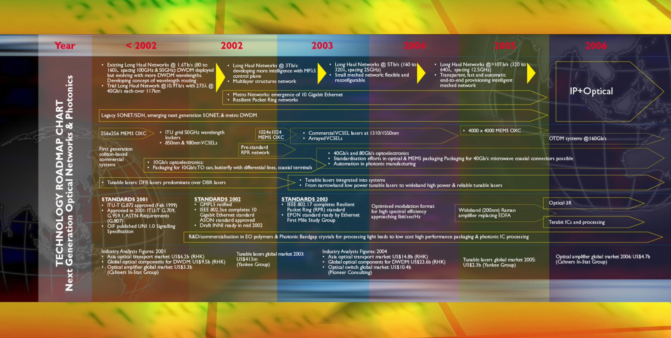

I n f o c o m m T e c h n o l o g y R o a d m a p R e l e a s e F e b r u a r y 2 0 0 2
96
GLOSSARY
I n f o c o m m T e c h n o l o g y R o a d m a p R e l e a s e F e b r u a r y 2 0 0 2
97
Glossary
10 GEA 10 Gigabit Ethernet Alliance10GbE 10 Gigabit Ethernet. Emerging IEEE standard for Ethernet at 10Gb/s. 3G Third Generation ACA Anisotropic Conductive AdhesiveADM Add/Drop MultiplexerADSL Asymmetric Digital Subscriber LineAOTF Acousto-Optic Tunable FilterAPON ATM Passive Optical NetworkARP Address Resolution Protocol. Protocol for mapping IP addresses to MAC addressesASE Amplied Spontaneous EmissionASIC Application Specic Integrated CircuitASON Automatic Switch Optical NetworkASTN Automatic Switch Transport NetworkATM Asynchronous Transfer Mode AWG Arrayed Waveguide GratingBER Bit Error RateBGA Ball Grid Array. Surface-mounted package with metal balls arranged in a grid pattern on the back of the packageBPON Broadband Passive Optical NetworkC-band Conventional bandCA*net, CA*net II, CA*net 3 Leading Canadian research and education networks, developed by CANARIE.CD Chromatic DispersionCDMA Code Division Multiple AccessCLEC Competitive Local Exchange CarrierCLIP Classical Internet ProtocolCMOS Complementary Metal Oxide SemiconductorCO2 Laser Carbon Dioxide LaserCPE Customer Premise EquipmentCR-LDP Constraint-based Routing LDP CSP Chip Scale PackagingCWDM Coarse Wavelength Division MultiplexingDBA Dynamic Bandwidth AssignmentDBR Laser Distributed Bragg Reector LaserDCF Dispersion Compensating FibreDCM Dispersion Compensator ModuleDCS Digital Crossconnect SystemDFB Laser Distributed Feedback LaserDIP Dual-Inline PackageDLCI Data Link Connection Identier DPT Dynamic Packet TransportDRP Disaster Recovery PlanningDSF Dispersion Shifted FibreDSL Digital Subscriber LineDWDM Dense Wavelength Division MultiplexingE1 Represents speed of 2.048Mb/sEAM Electro Absorptive Modulator
GLO
SS
AR
Y

I n f o c o m m T e c h n o l o g y R o a d m a p R e l e a s e F e b r u a r y 2 0 0 2
98
ECL External Cavity LaserEDFA Erbium Doped Fibre AmplierEDWA Erbium Doped Waveguide AmplierEFM Ethernet in the First MileENNI External Node to Node InterfaceEOM Electro Optical ModulatorEPON Ethernet Passive Optical NetworkEr ErbiumESCON Enterprise Systems Connection. Registered trademark of IBM Corporation.FBG Fibre Bragg GratingFDDI Fibre Distributed Data Interface. A standard for 100Mb/s bre-optic local area networkFEC Forward Error Correction FEC Forward Equivalence ClassFR Frame RelayFSAN Full Service Access NetworkFTTx Fibre-to-the-Curb (FTTC), Fibre-to-the-Building (FTTB), Fibre-to-the- Cabinet (FTTCab), Fibre-to-the-Ofce (FTTO) or Fibre-to-the-Home (FTTH)FWM Four Wave MixingGaAs Gallium ArsenideGb/s Giga-bit-per-secondGbE Gigabit EthernetGHz Giga HertzGMPLS Generalised Multiprotocol Label SwitchingHBT Heterojunction Bipolar TransistorHFC Hybrid-Fibre CoaxialI/O Input/OutputIA Implementation AgreementIBBMM Interactive Broadband MultimediaIC Integrated CircuitICA Isotropic Conductive AdhesiveICT Information and Communication TechnologyIEEE Institute of Electrical and Electronic Engineers IETF Internet Engineering Task ForceILEC Incumbent Local Exchange CarrierINNI Internal Node to Node InterfaceInP Indium PhosphideIP Internet ProtocolISDN Integrated Services Digital NetworkISP Internet Service ProviderITR Infocomm Technology RoadmapITU International Telecommunications UnionIXC Inter-eXchange CarriersL-band Long bandLAN Local Area NetworkLDP Label Distribution ProtocolLED Light Emitting DiodeLEX Local ExchangeLIB Label Information BaseLIGA Acronym from German words Lithographie, Galvanoformung, Abformung, meaning lithography, electroplating and moulding
GLOSSARY
I n f o c o m m T e c h n o l o g y R o a d m a p R e l e a s e F e b r u a r y 2 0 0 2
99
LiNbO3 Lithium NiobateLMSC LAN/MAN Standards CommitteeLSR Label Switching RouterMAC Media Access ControlMAN Metropolitan Area NetworkMb/s Mega-bit-per-secondMEMS MicroElectroMechanical SystemMESFET Metal-Semiconductor Field-Effect TransistorMetro Metropolitan MMF Multimode FibreMNC Multi National CompanyMOEMS Micro-Opto-Electro-Mechanical SystemMPLS Multiprotocols Label SwitchingMSM Metal-Semiconductor-MetalMSPP Multi Service Provisioning PlatformNGI Next Generation InternetNGN Next Generation Networknm Nanometres (10E-9)NNI Node to Node InterfaceO-UNI Optical User to Network InterfaceOADM Optical Add-Drop MultiplexerOAM Operation, Administration and Maintenance OAM&P Operations, Administration, Maintenance and Provisioning OCh Optical ChannelOC-xxx Optical Carrier. OC-x where the “x” represents increments of 51.84Mb/s. i.e. OC-1/STS-1, OC-3/STS-3, OC-12, OC-48 and OC-192 denote transmission standards for bre-optic data transmission in SONET frames at data rates of 51.84Mb/s, 155.52Mb/s, 622.08Mb/s, 2.48832Gb/s, and 9.95Gb/s, respectivelyOEIC Optical Electronics Integrated CircuitOEO Optical-Electrical-OpticalOIF Optical Internetworking ForumOLT Optical Line Terminating EquipmentOMS Optical Multiplex SectionON Optical NetworkONFIG Optical Network Focus Interest GroupONU Optical Network UnitOOO Optical-Optical-Optical Optical 1R Optical Re-amplicationOptical 2R Optical Re-amplication and ReshapingOptical 3R Optical Re-amplication, Re-timing, ReshapingOSNR Optical Signal to Noise RatioOSPF Open Shortest Path First. A routing protocol used in IP networksOTDM Optical Time Division MultiplexingOTN Optical Transport NetworkOTS Optical Transmission SectionOXC Optical CrossconnectPCF Photonic Crystal FibrePDH Pleisochronous Digital HierarchyPGA Pin Grid Array. Package for through-hole mounting with pins arrayed on the entire base plane
GLO
SS
AR
Y

I n f o c o m m T e c h n o l o g y R o a d m a p R e l e a s e F e b r u a r y 2 0 0 2
100
PHEMT Pseudomorphic high-electron-mobility transistorPHY Refers to Physical layerPIN Positive-Intrinsic-Negative diodePLC Planar Lightwave CircuitPMD Polarisation Mode DispersionPON Passive Optical NetworkPOP Point of Presence. A term used by ISPs to indicate the number of geographical locations from which they provide access to the InternetPOS Packet Over SONETPPP Point-to-Point ProtocolPVC Permanent Virtual CircuitPXC Photonics CrossconnectQFP Quad Flat PackQoS Quality of ServiceR&D Research and DevelopmentRF Radio FrequencyRIC Research Institution and CentreRIE Reactive Ion EtchingRPR Resilient Packet RingRSVP resource ReSerVation ProtocolS Band Short BandSAB Surface Activated BondingSAN Storage Area NetworkSC Standard ConnectorSDH Synchronous Digital Hierarchy (European term) SDL Simplied Data LinkSFF Small Form Factor (term used with connectors)SMF Single Mode FibreSOA Semiconductor Optical AmplierSOL GEL The sol-gel process is a versatile solution process for making ceramic and glass materials. Sol-gel process involves the transition of a system from a liquid “sol” into a solid “gel” phase. SONET Synchronous Optical Network (North American term)SPM Self Phase ModulationSRP Spatial Reuse Protocol. A proprietary Cisco packet ring based on DPT technologyST Straight TipSTM Synchronous Transfer ModeSTS Synchronous Transport Signal. A fundamental unit of 51.84Mb/s in the SONET hierarchy, with “n” representing the integral multiples. The most common values of “n” are 1, 3, 6, and 12. SWDM Sparse Wavelength Division MultiplexingT1 Represents speed of 1.544Mb/sTb/s Tera bit-per-secondTDM Time Division MultiplexingTE Trafc EngineeringTm ThuliumTSOP Thin Small Outline Packaging UDWDM Ultra Dense Wavelength Division MultiplexingUNI User Network InterfaceUSF Dispersion Unshifted Fibre
GLOSSARY

I n f o c o m m T e c h n o l o g y R o a d m a p R e l e a s e F e b r u a r y 2 0 0 2
101
VCI Virtual Circuit IdentierVCSEL Vertical Cavity Surface Emitting LaserVOA Variable Optical AttenuatorVPI Virtual Path IdentierVSR Very Short ReachWAN Wide Area NetworkWBGA Window Ball Grid ArrayWDM Wavelength Division Multiplexing WG Working GroupYAG Laser Yttrium Aluminium Garnet Laserλ ‘lambda’, meaning wavelength
GLO
SS
AR
Y

I n f o c o m m T e c h n o l o g y R o a d m a p R e l e a s e F e b r u a r y 2 0 0 2
102
FEEDBACK

I n f o c o m m T e c h n o l o g y R o a d m a p R e l e a s e F e b r u a r y 2 0 0 2
103
FEEDBACK
This Infocomm Technology Roadmap is a continuous effort, to be revised and updated as technologies evolve. For enquiry, proposals on technology development and initiatives, you can reach us at:
Website: http://www.ida.gov.sg (Click on “Technology Development”, followed by “Infocomm Technology Roadmap”)
Email: [email protected]
Infocomm Technology RoadmapTechnology Direction
Chief Technology OfceInfocomm Development Authority of Singapore
8 Temasek Boulevard#14-00 Suntec Tower Three
Singapore 038988
FEE
DB
AC
K

I n f o c o m m T e c h n o l o g y R o a d m a p R e l e a s e F e b r u a r y 2 0 0 2
104
SURVEY FORM

I n f o c o m m T e c h n o l o g y R o a d m a p R e l e a s e F e b r u a r y 2 0 0 2
105
SU
RV
EY
F0R
M
Survey Form

I n f o c o m m T e c h n o l o g y R o a d m a p R e l e a s e F e b r u a r y 2 0 0 2
106
SURVEY FORM
Survey Form
IDA Technology Roadmap 2002
Track 1: Next Generation Optical Networks & Photonics
With active contribution from the industry and research community, IDA has launched the Infocomm Technology Roadmap Release February 2002. You have either attended the Roadmap Symposium or downloaded a copy of the Technology Roadmap document from our website. Your feedback is valuable to us to better our future services for you. We appreciate if you could spare a few minutes to fill up the following survey.
Please return the completed questionnaire to IDA:
via Fax: +(65) 211 2211 (Attention to Ms Saliza Mohd)
or via Mail to the address on the previous page.
Company Name :
Your Name :
Designation/ :
Area of Expertise :
Email Address :
Contact Number :
Q1. With regards to the Roadmap Report Release Feb 2002 Track 1, please rate the following on a scale of 1 to 5.
Factors Excellent PoorUsefulness of the roadmap 5 4 3 2 1Completeness of coverage and contents 5 4 3 2 1Ease of understanding 5 4 3 2 1Usefulness of the Roadmap Chart 5 4 3 2 1Relevance to you or to your business strategy/ 5 4 3 2 1planning
Comments (if any):

I n f o c o m m T e c h n o l o g y R o a d m a p R e l e a s e F e b r u a r y 2 0 0 2
107
SU
RV
EY
F0R
M
Q2. Please indicate the accuracy (in terms of trend & development) of each topic in the Technology Roadmap Report. Please rate them on a scale of 1 to 5.
Area/Topic Accurate InaccurateNext Generation Optical Networks 5 4 3 2 1Photonics Enabling Technologies 5 4 3 2 1Standard Development 5 4 3 2 1Singapore Landscape 5 4 3 2 1Roadmap Chart 5 4 3 2 1
Comments (if any):
Q3. Do you have any suggestions for improvement on the Technology Roadmap?
Q4. If you are an industry player in Optical Networking & Photonics, what are the services, facilities, equipment and supporting infrastructure that you need but are lacking in Singapore?
Q5. Would you like to be informed of our future Infocomm Technology Roadmap Symposiums/Reports?
Yes / No
Thank You