tape and reel packaging for semiconductor devices
TRANSCRIPT
Tape and Reel Packaging for Semiconductor Devices
Technical Data
DescriptionThis data sheet is intended to cover standards on tape and reel packaging for Avago Technologies’s semicon-ductor devices. This type of tape and reel packaging is designed to be compatible with available automated pick and place machines.
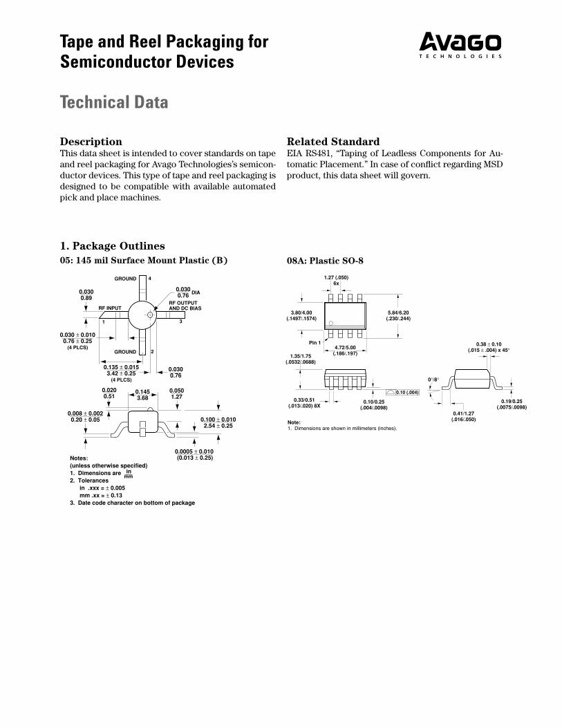
1. Package Outlines05: 145 mil Surface Mount Plastic (B) 08A: Plastic SO-8
4
0.0300.89
0.100 ± 0.0102.54 ± 0.25
0.135 ± 0.0153.42 ± 0.25
(4 PLCS)
1 3
2
0.008 ± 0.0020.20 ± 0.05
0.0005 ± 0.010 (0.013 ± 0.25)
0.0501.27
GROUND
RF INPUTRF OUTPUTAND DC BIAS
GROUND
0.0300.76
0.0300.76
0.1453.68
0.0200.51
DIA
0.030 ± 0.0100.76 ± 0.25
(4 PLCS)
Notes:(unless otherwise specified)1. Dimensions are in
2. Tolerances in .xxx = ± 0.005 mm .xx = ± 0.133. Date code character on bottom of package
mm
5.84/6.20(.230/.244)
3.80/4.00(.1497/.1574)
Pin 1
1.27 (.050)6x
4.72/5.00(.186/.197)
0.10/0.25(.004/.0098)
0.33/0.51(.013/.020) 8X
1.35/1.75(.0532/.0688)
0.19/0.25(.0075/.0098)
0.41/1.27(.016/.050)
0°/8°
0.38 ± 0.10(.015 ± .004) x 45°
0.10 (.004)
Note:1. Dimensions are shown in millimeters (inches).
Related StandardEIA RS481, “Taping of Leadless Components for Au-tomatic Placement.” In case of conflict regarding MSD product, this data sheet will govern.
�
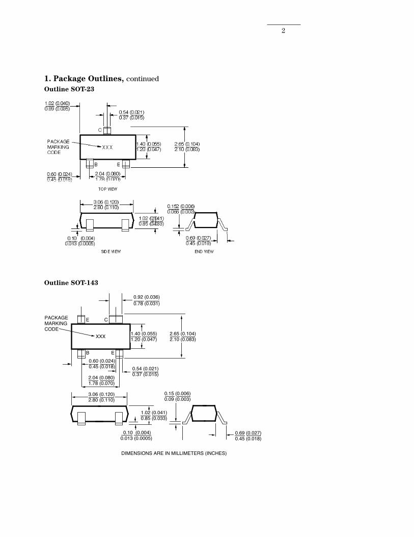
1. Package Outlines, continuedOutline SOT-23
Outline SOT-143
DIMENSIONS ARE IN MILLIMETERS (INCHES)
0.10 (0.004) 0.013 (0.0005)
0.92 (0.036)0.78 (0.031)
E
E
B
C
XXX
PACKAGEMARKINGCODE
1.40 (0.055)1.20 (0.047)
2.65 (0.104)2.10 (0.083)
0.54 (0.021)0.37 (0.015)
0.60 (0.024)0.45 (0.018)
2.04 (0.080)1.78 (0.070)
3.06 (0.120)2.80 (0.110)
0.15 (0.006)0.09 (0.003)
1.02 (0.041)0.85 (0.033)
0.69 (0.027)0.45 (0.018)
�
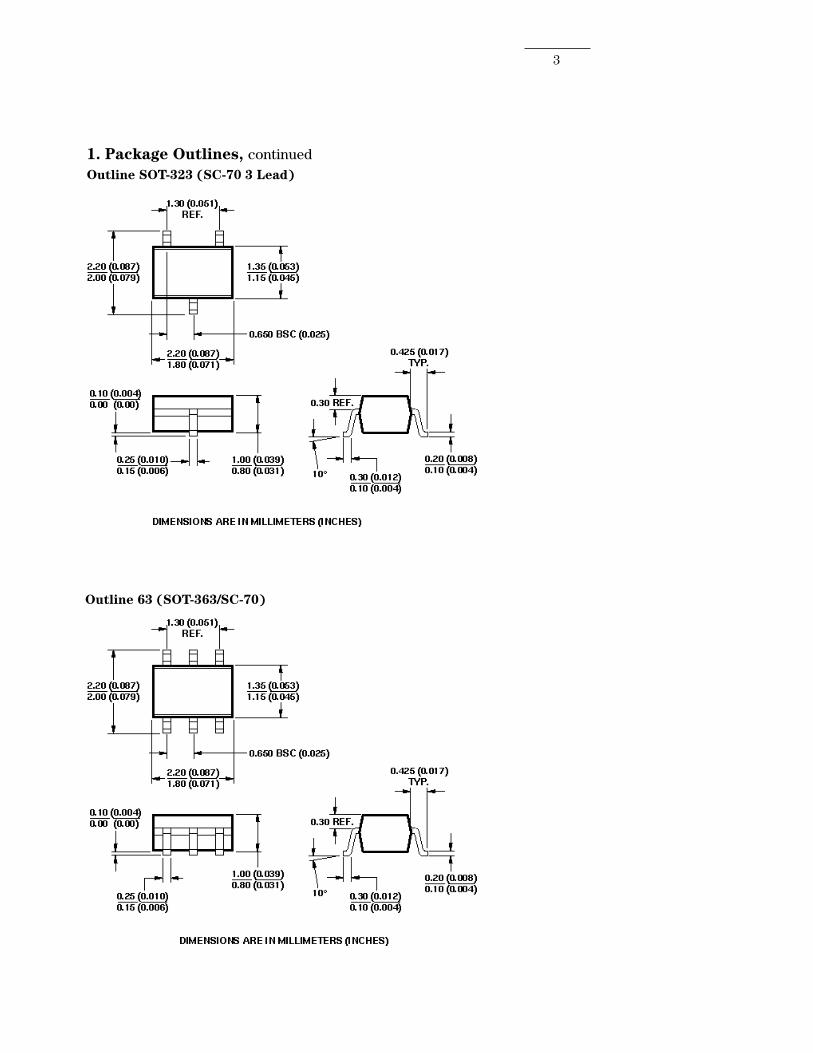
1. Package Outlines, continuedOutline SOT-323 (SC-70 3 Lead)
Outline 63 (SOT-363/SC-70)

4
1. Package Outlines, continuedOutline TQFP-32 (32 Pin Thin Quad Flat Package)
Outline TQFP-48 (48 Pin Thin Quad Flat Package)
�
1. Package Outlines, continued
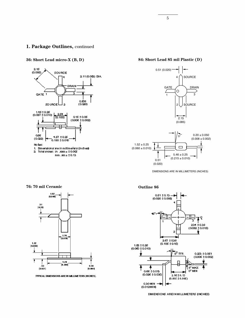
36: Short Lead micro-X (B, D) 84: Short Lead 85 mil Plastic (D)
1
4
3
2
0.51 (0.020)
0.51 (0.020)
DIMENSIONS ARE IN MILLIMETERS (INCHES)DATE CODE MARK ON BOTTOM OF PACKAGE
0.20 ± 0.050(0.008 ± 0.002)
2.15(0.085)
1.52 ± 0.25(0.060 ± 0.010)
5.46 ± 0.25 (0.215 ± 0.010)
5°
SOURCE
DRAIN
SOURCE
GATE
Outline 8676: 70 mil Ceramic
�
1. Package Outlines, continued
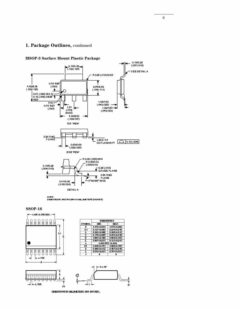
MSOP-3 Surface Mount Plastic Package
SSOP-16
�
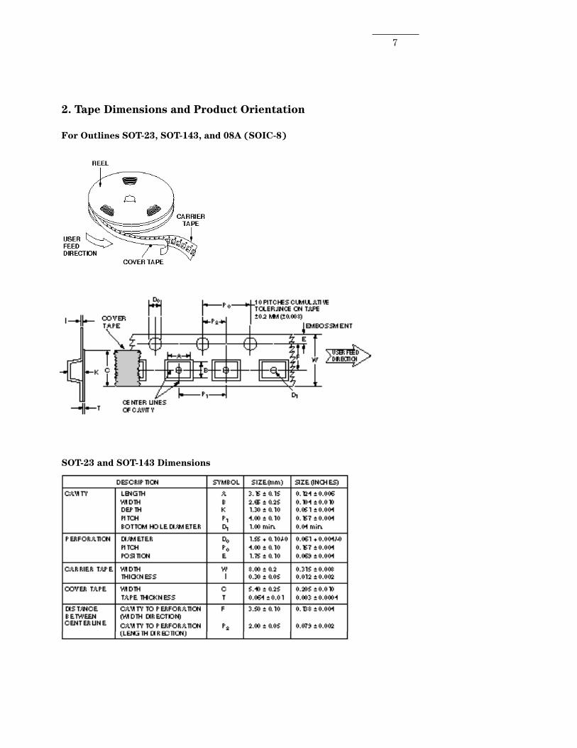
2. Tape Dimensions and Product Orientation
For Outlines SOT-23, SOT-143, and 08A (SOIC-8)
SOT-23 and SOT-143 Dimensions
8
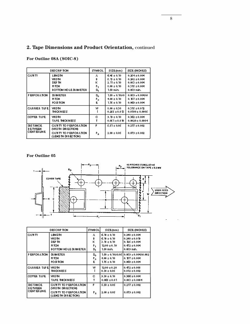
2. Tape Dimensions and Product Orientation, continued
For Outline 08A (SOIC-8)
For Outline 05
add line to bottom of table in Illust file
�
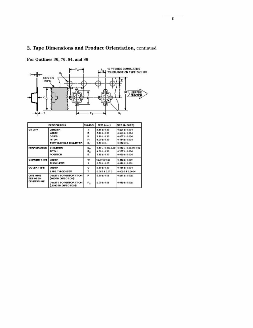
2. Tape Dimensions and Product Orientation, continued
For Outlines 36, 76, 84, and 86
10
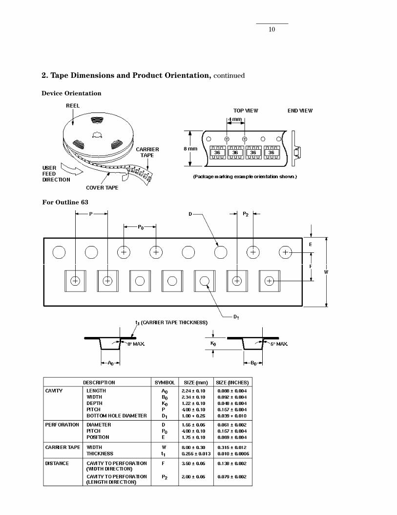
2. Tape Dimensions and Product Orientation, continued
Device Orientation
For Outline 63
11
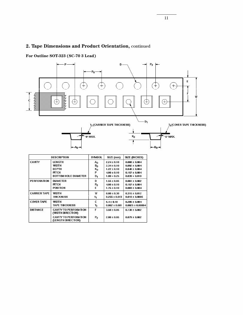
2. Tape Dimensions and Product Orientation, continued
For Outline SOT-323 (SC-70 3 Lead)
1�
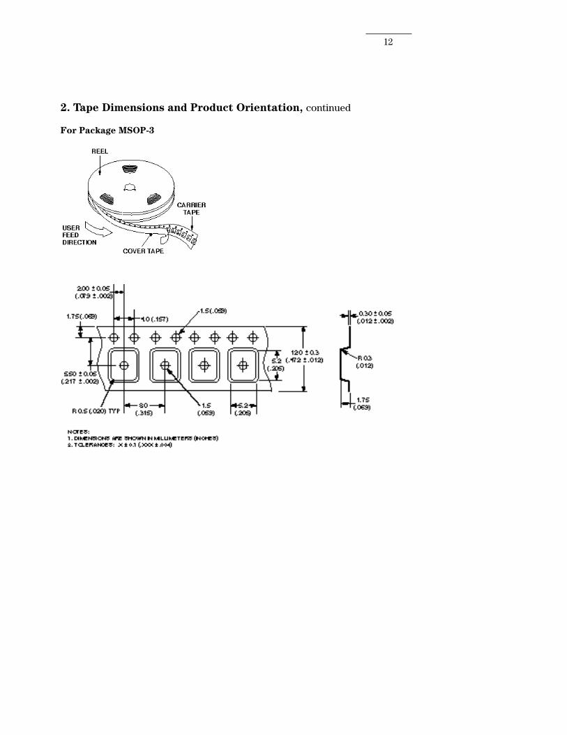
2. Tape Dimensions and Product Orientation, continued For Package MSOP-3

1�
2. Tape Dimensions and Product Orientation, continued For Package SSOP-16
14
2. Tape Dimensions and Product Orientation, continued
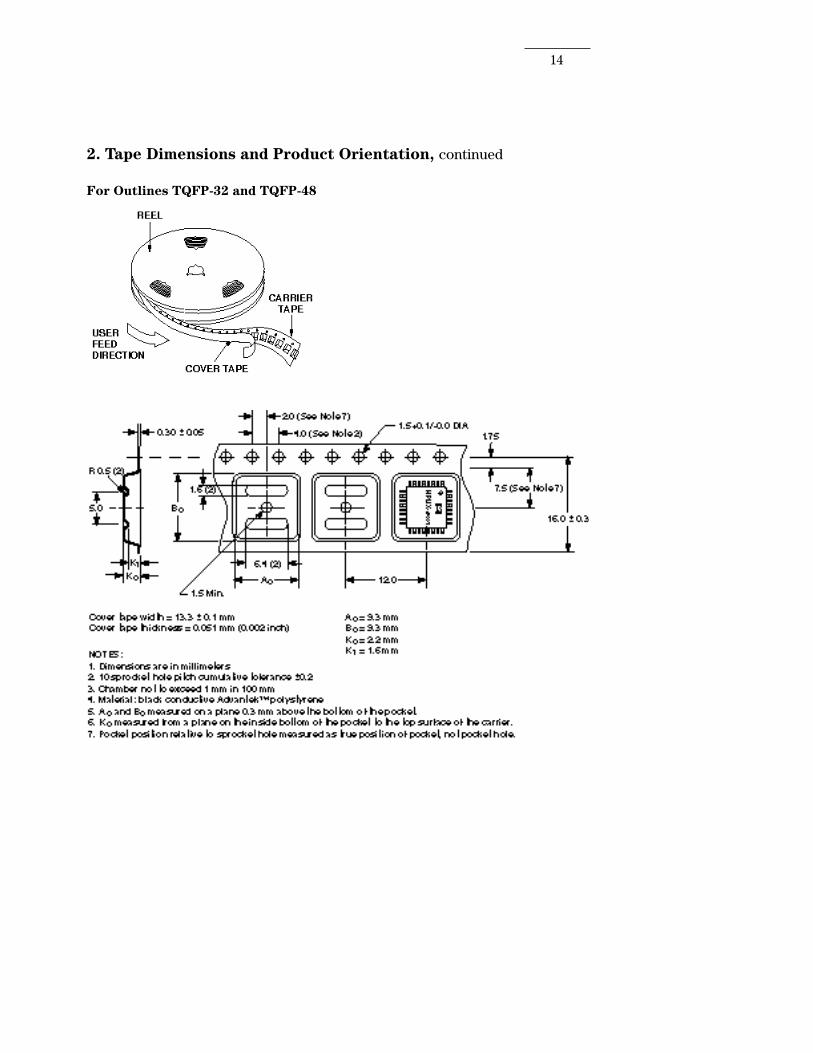
For Outlines TQFP-32 and TQFP-48
1�
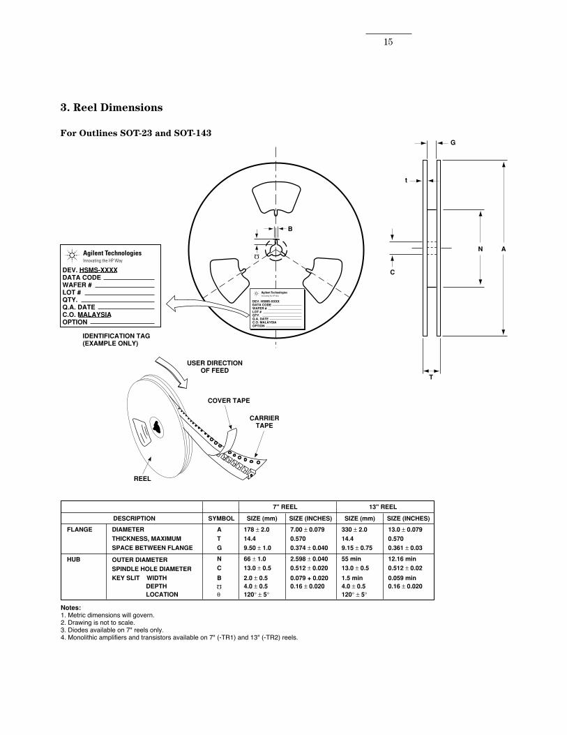
3. Reel Dimensions
For Outlines SOT-23 and SOT-143
CARRIERTAPE
REEL
COVER TAPE
IDENTIFICATION TAG(EXAMPLE ONLY)
USER DIRECTIONOF FEED
DEV. HSMS-XXXXDATA CODEWAFER #LOT #QTY.Q.A. DATEC.O. MALAYSIAOPTION
DEV. HSMS-XXXXDATA CODEWAFER #LOT #QTY.Q.A. DATEC.O. MALAYSIAOPTION
Ω
C
B
G
T
t
N A
DESCRIPTION SYMBOL SIZE (mm)
7" REEL
SIZE (INCHES)
DIAMETER
THICKNESS, MAXIMUM
SPACE BETWEEN FLANGE
OUTER DIAMETER
SPINDLE HOLE DIAMETER
A
T
G
N
C
178 ± 2.0
14.4
9.50 ± 1.0
66 ± 1.0
13.0 ± 0.5
7.00 ± 0.079
0.570
0.374 ± 0.040
2.598 ± 0.040
0.512 ± 0.020
FLANGE
KEY SLIT WIDTHDEPTHLOCATION
B
Ω
θ
2.0 ± 0.54.0 ± 0.5120° ± 5°
0.079 + 0.0200.16 ± 0.020
SIZE (mm)
13" REEL
SIZE (INCHES)
330 ± 2.0
14.4
9.15 ± 0.75
55 min
13.0 ± 0.5
13.0 ± 0.079
0.570
0.361 ± 0.03
12.16 min
0.512 ± 0.02
1.5 min4.0 ± 0.5120° ± 5°
0.059 min0.16 ± 0.020
HUB
Notes:1. Metric dimensions will govern. �2. Drawing is not to scale. �3. Diodes available on 7" reels only. �4. Monolithic amplifiers and transistors available on 7" (-TR1) and 13" (-TR2) reels. ��
1�
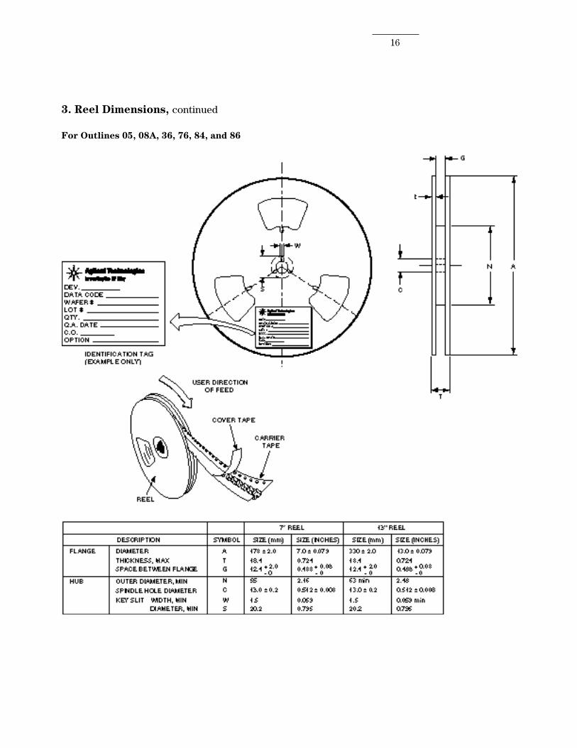
3. Reel Dimensions, continued
For Outlines 05, 08A, 36, 76, 84, and 86
1�
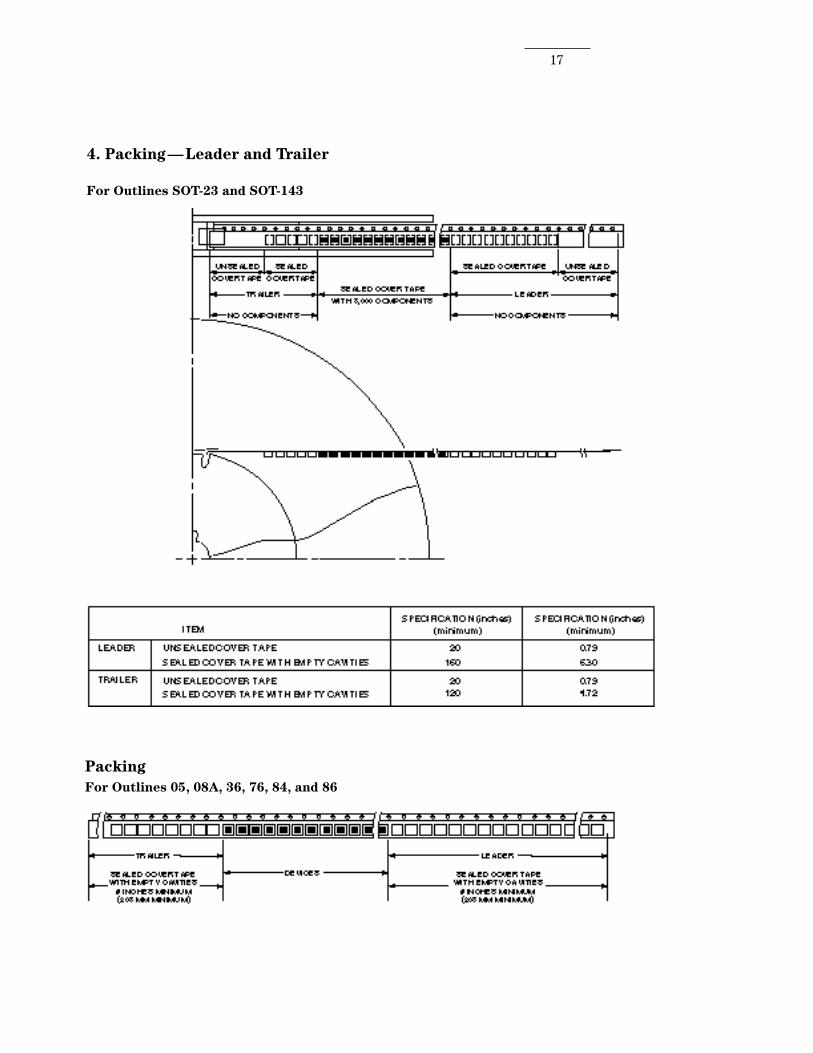
4. Packing—Leader and Trailer
For Outlines SOT-23 and SOT-143
PackingFor Outlines 05, 08A, 36, 76, 84, and 86
18
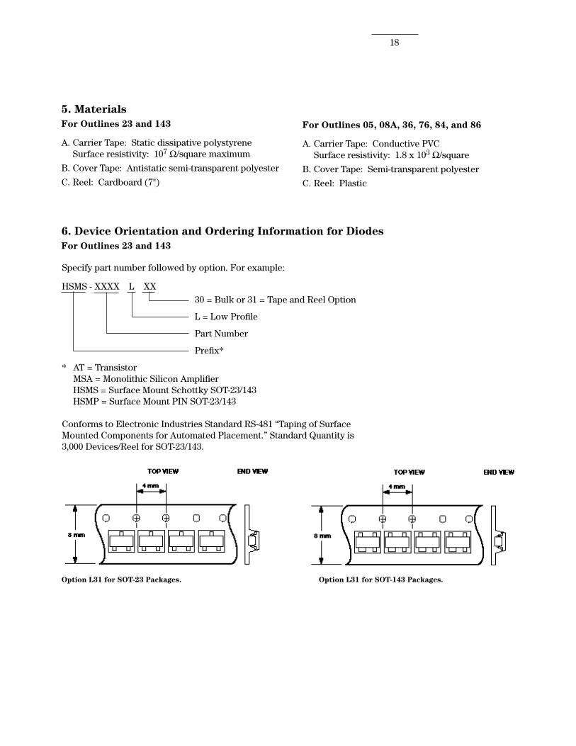
5. MaterialsFor Outlines 23 and 143
A. Carrier Tape: Static dissipative polystyrene Surface resistivity: 10� Ω/square maximum
B. Cover Tape: Antistatic semi-transparent polyester
C. Reel: Cardboard (�")
6. Device Orientation and Ordering Information for DiodesFor Outlines 23 and 143
Specify part number followed by option. For example:
HSMS - XXXX L XX �0 = Bulk or �1 = Tape and Reel Option
L = Low Profile
Part Number
Prefix*
* AT = Transistor MSA = Monolithic Silicon Amplifier HSMS = Surface Mount Schottky SOT-��/14� HSMP = Surface Mount PIN SOT-��/14�
Conforms to Electronic Industries Standard RS-481 “Taping of Surface Mounted Components for Automated Placement.” Standard Quantity is �,000 Devices/Reel for SOT-��/14�.
For Outlines 05, 08A, 36, 76, 84, and 86
A. Carrier Tape: Conductive PVC Surface resistivity: 1.8 x 10� Ω/square
B. Cover Tape: Semi-transparent polyester
C. Reel: Plastic
Option L31 for SOT-23 Packages. Option L31 for SOT-143 Packages.
1�
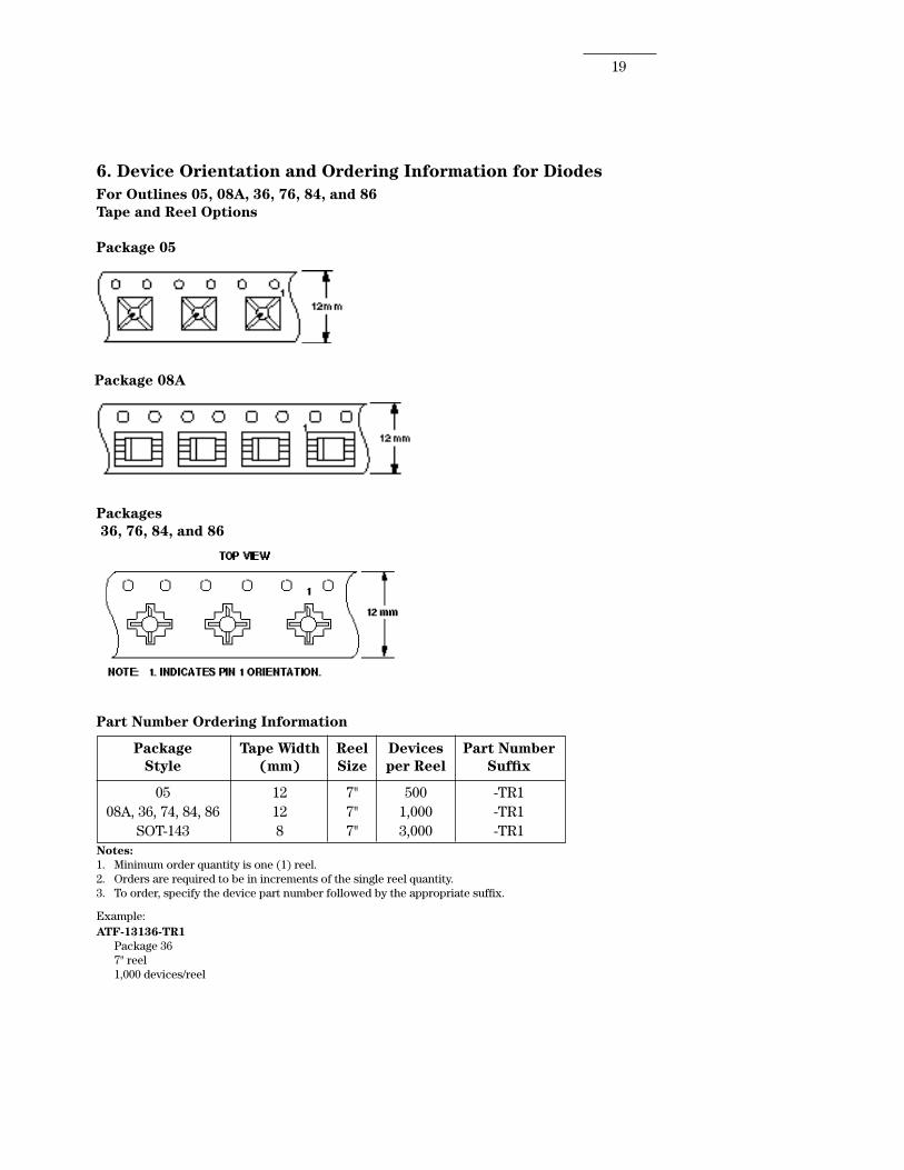
6. Device Orientation and Ordering Information for DiodesFor Outlines 05, 08A, 36, 76, 84, and 86Tape and Reel Options
Package 05
Packages 36, 76, 84, and 86
Part Number Ordering Information
Package Tape Width Reel Devices Part Number Style (mm) Size per Reel Suffix
0� 1� �" �00 -TR1 08A, ��, �4, 84, 8� 1� �" 1,000 -TR1 SOT-14� 8 �" �,000 -TR1Notes:1. Minimum order quantity is one (1) reel.�. Orders are required to be in increments of the single reel quantity.�. To order, specify the device part number followed by the appropriate suffix.
Example: ATF-13136-TR1
Package ���" reel1,000 devices/reel
Package 08A

For product information and a complete list of distributors, please go to our web site: www.avagotech.com
Avago, Avago Technologies, and the A logo are trademarks of Avago Technologies, Limited in the United States and other countries.Data subject to change. Copyright © 2007 Avago Technologies Limited. All rights reserved. Obsoletes 5091-2201E5966-3702E - November 1, 2007