tas5631dkd2evm user's guide - ti · 3 physical structure for the tas5631dkd2evm (approximate...
TRANSCRIPT

User's GuideSLOU274A–November 2009–Revised May 2010
TAS5631DKD2EVM
This user’s guide describes the operation of the evaluation module for the TAS5631 Digital AmplifierPower Output Stage using TAS5518 Digital Audio PWM Processor from Texas Instruments. The user’sguide also provides measurement data and design information like schematic, BOM, and PCB layout.
Contents1 Introduction .................................................................................................................. 3
1.1 TAS5631DKD2EVM Features .................................................................................... 41.2 PCB Key map ...................................................................................................... 5
2 Quick Setup Guide .......................................................................................................... 52.1 Electrostatic Discharge Warning ................................................................................. 52.2 Unpacking the EVM ................................................................................................ 62.3 Power Supply Setup ............................................................................................... 62.4 Speaker Connection ............................................................................................... 62.5 Output configuration BTL and PBTL ............................................................................ 62.6 GUI Software Installation .......................................................................................... 7
3 Protection .................................................................................................................... 83.1 Short Circuit Protection and Fault Reporting Circuitry ........................................................ 83.2 Fault Reporting ..................................................................................................... 8
4 TAS5631DKD2EVM Performance ........................................................................................ 94.1 THD+N vs. Power ................................................................................................ 114.2 THD+N vs. Frequency ........................................................................................... 124.3 FFT Spectrum ..................................................................................................... 134.4 Idle Noise FFT Spectrum ........................................................................................ 144.5 Channel Separation .............................................................................................. 154.6 Frequency Response ............................................................................................ 164.7 High Current Protection .......................................................................................... 174.8 Pop/Click ........................................................................................................... 184.9 Output Stage Efficiency .......................................................................................... 19
5 Related Documentation from Texas Instruments ..................................................................... 205.1 Additional Documentation ....................................................................................... 20
Appendix A Design Documents ............................................................................................... 20
List of Figures
1 TAS5631DKD2EVM – Top View.......................................................................................... 4
2 Integrated PurePath Digital™ Amplifier System ........................................................................ 4
3 Physical Structure for the TAS5631DKD2EVM (Approximate Layout) .............................................. 5
4 PBTL Mode Configuration ................................................................................................. 7
5 TAS5518 GUI Window ..................................................................................................... 8
6 THD+N vs. Power (BTL – 4 Ω) .......................................................................................... 11
7 THD+N vs. Power (BTL – 8 Ω) .......................................................................................... 11
8 THD+N vs. Power (PBTL – 2 Ω) ........................................................................................ 12
9 THD+N vs. Frequency (BTL – 4 Ω) ..................................................................................... 12
10 THD+N vs. Frequency (BTL – 8 Ω) ..................................................................................... 13
PurePath, Equibit are trademarks of Texas Instruments.I2C is a trademark of NXP B.V. Corp Netherlands.
1SLOU274A–November 2009–Revised May 2010 TAS5631DKD2EVM
Copyright © 2009–2010, Texas Instruments Incorporated

www.ti.com
11 THD+N vs. Frequency (PBTL – 2 Ω) .................................................................................. 13
12 FFT Spectrum with -60 dBFS Tone (BTL) ............................................................................. 14
13 FFT Spectrum with -60 dBFS Tone (PBTL) ........................................................................... 14
14 Idle Noise FFT Spectrum (BTL) ......................................................................................... 15
15 Idle Noise FFT Spectrum (PBTL) ....................................................................................... 15
16 Channel Separation ....................................................................................................... 16
17 Frequency Response (BTL).............................................................................................. 16
18 Frequency Response (PBTL) ............................................................................................ 17
19 High Current Protection (BTL) ........................................................................................... 17
20 High Current Protection (PBTL) ......................................................................................... 18
21 Pop/Click (BTL) ............................................................................................................ 18
22 Pop/Click (PBTL) .......................................................................................................... 19
23 Output Stage Efficiency................................................................................................... 19
List of Tables
1 TAS5631DKD2EVM Specification ........................................................................................ 3
2 Table 2. Recommended Supply Voltages .............................................................................. 6
3 TAS5631 Warning/Error Signal Decoding ............................................................................... 9
4 General Test Conditions ................................................................................................... 9
5 TAS5518 Register Settings................................................................................................ 9
6 Electrical Data ............................................................................................................... 9
7 Audio Performance ........................................................................................................ 10
8 Thermal Specification ..................................................................................................... 10
9 Physical Specifications ................................................................................................... 10
10 Related Documentation from Texas Instruments ..................................................................... 20
2 TAS5631DKD2EVM SLOU274A–November 2009–Revised May 2010
Copyright © 2009–2010, Texas Instruments Incorporated

www.ti.com Introduction
1 Introduction
The TAS5631DKD2EVM PurePath™ HD customer evaluation module demonstrates the integrated circuitsTAS5631DKD and TAS5518PAG from Texas Instruments.
The TAS5631DKD is a high-performance, integrated Stereo Feedback Digital Amplifier Power Stagedesigned to drive 4-Ω speakers at up to 300 W per channel. The device incorporates the TI Equibit™technology and is designed to be used with TI’s Equibit™ modulators. This system only requires a passivedemodulation filter to deliver a efficiency, quality audio amplification.
TAS5518PAG is a high performance 32 bit (24 bit input) multi channel PurePath™ Digital Pulse WidthModulator (PWM) based on Equibit™ technology with fully symmetrical AD modulation scheme. Thedevice also has Digital Audio Processing (DAP) that provides 48 bit signal processing, advancedperformance and a high level of system integration. The device has interfaces for headphone output andPower Supply Volume Control (PSVC).
This EVM is configurable to 2 BTL channels for stereo evaluation or 1 PBTL (parallel BTL) channel forsubwoofer evaluation.
This EVM, together with a TI input-USB board 2, is a complete stereo digital audio amplifier system whichincludes digital input (S/PDIF), analog inputs, interface to PC and DAP features like digital volume control,input and output mixers, automute, tone controls, loudness, EQ filters and dynamic range compression(DRC). There are configuration options for power stage failure protection.
Table 1. TAS5631DKD2EVM Specification
Key Parameters Values
Output Stage Supply Voltage 25V – 50 V
Number of Channels 2 x BTL or 1 x PBTL
Load Impedance BTL 4-8 ΩLoad Impedance PBTL 2-3 Ω
Output power BTL 330 W / 4 Ω 10% THD or 180 W / 8 Ω / 10% THD
Output power PBTL 600 W / 2 Ω / 10% THD
DNR >105 dB
PWM Processor TAS5518PAG
Output Stage TAS5631DKD
3SLOU274A–November 2009–Revised May 2010 TAS5631DKD2EVM
Copyright © 2009–2010, Texas Instruments Incorporated

I2S
Bus
TAS5631DKD2EVM
MODULE
I2C Bus
Example
TI Input - USBboard
8 ChannelAnalog
Input
USBInterface
Opticaland
CoaxialS/PDIFInput
Control Interface
Power Supply
Stereo/Mono
ChannelSpeaker Output
Introduction www.ti.com
This document covers EVM specifications, audio performance and power efficiency measurementsgraphs, and design documentation that includes schematics, parts list, layout, and mechanical design.
Figure 1. TAS5631DKD2EVM – Top View
Gerber (layout) files are available at: www.ti.com.
The EVM is delivered with cables and Input-USB board 2 to connect to an input source, and be controlledfrom a PC.
1.1 TAS5631DKD2EVM Features• Stereo PurePath Digital™ evaluation module.• Self-contained protection system (short circuit and thermal).• Standard I2S and I2C™ / Control connector for TI input board• Double-sided plated-through PCB layout.
Figure 2. Integrated PurePath Digital™ Amplifier System
4 TAS5631DKD2EVM SLOU274A–November 2009–Revised May 2010
Copyright © 2009–2010, Texas Instruments Incorporated

+50 V(J15)
LEFTSPEAKEROUTPUT
(J12)
RIGHTSPEAKEROUTPUT
(J14)
(SW1)
(SW2)
PBTL
PBTLBTL
BTLTAS5518
INPUT SIGNAL& CONTROLINTERFACE(J10)
+12V
Fan
OU
TP
UT
CO
NT
RO
L(J
22)
+12V
Fan
Regula
tor
+3.3
VR
egula
tor
OU
TP
UT
STA
GE
CH
AN
NE
LR
iGH
T
OU
TP
UT
STA
GE
CH
AN
NE
LLE
FT
www.ti.com Quick Setup Guide
1.2 PCB Key map
Physical structure for the TAS5631DKD2EVM is illustrated in Figure 3.
Figure 3. Physical Structure for the TAS5631DKD2EVM (Approximate Layout)
2 Quick Setup Guide
This section describes the TAS5631DKD2EVM board in regards to power supplies and system interfaces.The section provides information regarding handling and unpacking, absolute operating conditions, and adescription of the factory default switch and jumper configuration.
This section also provides a step–by–step guide to configuring the TAS5631DKD2EVM for deviceevaluation.
2.1 Electrostatic Discharge Warning
Many of the components on the TAS5631DKD2EVM are susceptible to damage by electrostatic discharge(ESD). Customers are advised to observe proper ESD handling precautions when unpacking and handlingthe EVM, including the use of a grounded wrist strap at an approved ESD workstation.
CAUTION
Failure to observe ESD handling procedures can result in damage to EVMcomponents.
5SLOU274A–November 2009–Revised May 2010 TAS5631DKD2EVM
Copyright © 2009–2010, Texas Instruments Incorporated

Quick Setup Guide www.ti.com
2.2 Unpacking the EVM
Upon opening the TAS5631DKD2EVM package, check to make sure that the following items are included:
• 1 pc. TAS5631DKD2EVM board using one TAS5518PAG and one TAS5631DKD.• 1 pc. TI Input-USB board 2 for interfacing TAS5631DKD2EVM with SPDIF/analog sources and PC for
control.• 1 pc. Signal and Control Interface IDC cable for connection to an I2S front-end like the attached TI
Input-USB board 2.• 1 pc. Cable for connecting Input-USB board 2 to a USB port on a PC for TAS5518 control by software.• 1 pc. AC to DC External 15 V Power supply (System supply).• 4 pcs. AC Input Clips for External 15 V Power Supply (US, Europe, UK and Australia).• 1 pc. PurePath™ CD-ROM.
If any of these items are missing, contact the nearest Texas Instruments Product Information Center toinquire about a replacement.
Connect the Input-micro board to the TAS5631DKD2EVM using the delivered IDC cable.
2.3 Power Supply Setup
To power up the EVM, two power supplies are needed. One for system power, logic and gate-drive, andone for output stage supply. H-bridge Power supply is connected to the EVM using banana cables.System Power Supply is supplied from the enclosed External 15 V wall plug adapter.
Table 2. Table 2. Recommended Supply Voltages
Description Voltage Range Current Requirements Cable
Output stage power supply 25 – 50 V 16 A J15 (marked +50V)
CAUTION
Applying voltages above the specifications given in Table 2 can causepermenant damage to the hardware.
NOTE: The length of power supply cable must be minimized. Increasing length of PSU cable isequal to increasing the distortion for the amplifier at high output levels and low frequencies.
2.4 Speaker Connection
CAUTION
Both positive and negative speaker outputs are floating and cannot beconnected to ground (e.g. through an oscilloscope).
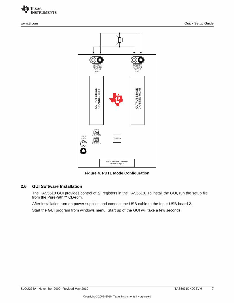
2.5 Output configuration BTL and PBTL
When changing mode e.g. from BTL to PBTL, make sure that RESET is activated before changing thestate of mode switches SW1 and SW2. Switch SW1 and SW2 has to be synchronized in state BTL orPBTL.
In PBTL mode the load has to be connected according to Figure 4:
6 TAS5631DKD2EVM SLOU274A–November 2009–Revised May 2010
Copyright © 2009–2010, Texas Instruments Incorporated
+50 V(J15)
LEFT BTLSPEAKEROUTPUT
(J11)
RIGHT BTLSPEAKEROUTPUT
(J13)
(SW1)
(SW2)
PBTL
PBTLBTL
BTL
INPUT SIGNAL& CONTROLINTERFACE(J10)
TAS5518O
UT
PU
TS
TA
GE
CH
AN
NE
LR
IGH
T
PB
LT
OU
TP
UT
STA
GE
CH
AN
NE
LL
EF
T
www.ti.com Quick Setup Guide
Figure 4. PBTL Mode Configuration
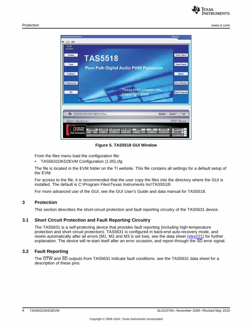
2.6 GUI Software Installation
The TAS5518 GUI provides control of all registers in the TAS5518. To install the GUI, run the setup filefrom the PurePath™ CD-rom.
After installation turn on power supplies and connect the USB cable to the Input-USB board 2.
Start the GUI program from windows menu. Start up of the GUI will take a few seconds.
7SLOU274A–November 2009–Revised May 2010 TAS5631DKD2EVM
Copyright © 2009–2010, Texas Instruments Incorporated
Protection www.ti.com
Figure 5. TAS5518 GUI Window
From the files menu load the configuration file:• TAS5631DKD2EVM Configuration (1.00).cfg
The file is located in the EVM folder on the TI website. This file contains all settings for a default setup ofthe EVM.
For access to the file, it is recommended that the user copy the files into the directory where the GUI isinstalled. The default is C:\Program Files\Texas Instruments Inc\TAS5518\
For more advanced use of the GUI, see the GUI User’s Guide and data manual for TAS5518.
3 Protection
This section describes the short-circuit protection and fault reporting circuitry of the TAS5631 device.
3.1 Short Circuit Protection and Fault Reporting Circuitry
The TAS5631 is a self-protecting device that provides fault reporting (including high-temperatureprotection and short circuit protection). TAS5631 is configured in back-end auto-recovery mode, andresets automatically after all errors (M1, M2 and M3 is set low), see the data sheet (sles221) for furtherexplanation. The device will re-start itself after an error occasion, and report through the SD error signal.
3.2 Fault Reporting
The OTW and SD outputs from TAS5631 indicate fault conditions. see the TAS5631 data sheet for adescription of these pins.
8 TAS5631DKD2EVM SLOU274A–November 2009–Revised May 2010
Copyright © 2009–2010, Texas Instruments Incorporated

www.ti.com TAS5631DKD2EVM Performance
Table 3. TAS5631 Warning/Error Signal Decoding
SD OTW1 OTW2 Device Condition
0 0 0 High temperature error and/or high current error
Under voltage lockout or high current error. 100°C0 0 1 temperature warning
0 1 1 Under voltage lockout or high current error
1 0 0 125°C temperature warning
1 0 1 100°C temperature warning
1 1 1 Normal operation, no errors/warnings
The shutdown signals together with the temperature warning signal, give the chip state information asdescribed in Table 3. Device fault reporting outputs are open-drain outputs.
4 TAS5631DKD2EVM Performance
Table 4. General Test Conditions
General Test Conditions (1) Value Notes
Output Stage Supply Voltage 50 V Laboratory Power Supply (EA-PS 7065-10A)
Load Impedance BTL 4-8 Ohm
Load Impedance PBTL 2 Ohm
Input Signal 1kHz Sine
Sampling Frequency 48 kHz
Gain setting in TAS5518 0 dB
Measurement Filter AES17 and AUX0025
TI Input Board Input-USB 2 Rev 1
EVM configuration file Ver 1.00 TAS5631DKD2EVM Configuration (1.00).cfg
(1) These test conditions are used for all tests, unless otherwise specified.
Table 5. TAS5518 Register Settings
Register (1) Value Notes
System Control Register 2 0x04 0x60 PWM Automute Detection Disabled
Master Volume Register 0xD9 00 00 00 48 Master Volume set to 0 dB
(1) These test conditions are used for all tests, unless otherwise specified.
Table 6. Electrical Data
General Test Conditions Value Notes
Output Power, BTL, 4Ω 180 W 1 kHz, unclipped (0dBFS), TA = 25°C
Output Power, BTL, 4Ω 330 W 1 kHz, 10% THD+N, TA = 25°C
Output Power, BTL, 8Ω 100 W 1 kHz, unclipped (0dBFS), TA = 25°C
Output Power, BTL, 8Ω 180 W 1 kHz, 10% THD+N, TA = 25°C
Output Power, PBTL, 2Ω 330 W 1 kHz, unclipped (0 dBFS), TA = 25°C
Output Power, PBTL, 2Ω 600 W 1 kHz, 10% THD+N, TA = 25°C, TC < 50°C
Maximum Peak Current, BTL >16 A 1 kHz burst, 1 Ohm, ROC = 24 kΩ
Maximum Peak Current, PBTL >28 A 1 kHz burst, 1 Ohm, ROC = 24 kΩ
Output Stage Efficiency >94 % 2 x channels, 8 Ω
Damping Factor BTL >16 1 kHz, relative to 4 Ω load
Damping Factor PBTL >18 1 kHz, relative to 2 Ω load
H-Bridge Supply Current <65 mA 1 kHz, -60dBFS signal
Idle Power Consumption 3.3 W H-Bridge supply, -60dBFS input signal
9SLOU274A–November 2009–Revised May 2010 TAS5631DKD2EVM
Copyright © 2009–2010, Texas Instruments Incorporated

TAS5631DKD2EVM Performance www.ti.com
Table 7. Audio Performance
Audio Performance Value Notes
THD+N, BTL, 4Ω 1 W <0.02 % 1 kHz
THD+N, BTL, 4Ω 10 W <0.02 % 1 kHz
THD+N, BTL, 4Ω 50 W <0.02 % 1 kHz
THD+N, BTL, 4Ω 200 W <0.5 % 1 kHz
THD+N, BTL, 8Ω 1 W <0.02 % 1 kHz
THD+N, BTL, 8Ω 10 W <0.02 % 1 kHz
THD+N, BTL, 8Ω 50 W <0.02 % 1 kHz
THD+N, BTL, 8Ω 100 W <0.5 % 1 kHz
THD+N, PBTL, 2Ω 1 W <0.02 % 1 kHz
THD+N, PBTL, 2Ω 10 W <0.02 % 1 kHz
THD+N, PBTL, 2Ω 100 W <0.03 % 1 kHz
THD+N, PBTL, 2Ω 200 W <0.05 % 1 kHz
THD+N, PBTL, 2Ω 400 W <0.5 % 1 kHz
Ref: rated power, A-weighted, AES17Dynamic Range >105 dB filter, 4 ch avg
Noise Voltage <190 mVrms A-weighted, AES17 filter
Click/Pop, DC step BTL 18 mV Mute/Unmute, No signal, 6 Ohm
Click/Pop, DC step PBT 18 mV Mute/Unmute, No signal, 4 Ohm
Channel Separation >80 dB 1 kHz
Frequency Response +0.5 / -1 dB 100 W / 8 Ω
Table 8. Thermal Specification
Thermal Specification (1) THEATSINK(1) Notes
Idle, All Channels Switching 28°C 1 kHz, 15 min, -60dBFS signal, TA = 25°C
2x40 W, 4Ω (1/8 power) 42°C 1 kHz, 1 hour, TA = 25°C
2x200 W, 4Ω 62°C 1 kHz, 5 min, TA = 25°C(1) Measured on surface of heat sink.
Table 9. Physical Specifications
Physical Specifications (1) Notes
PCB Dimensions 94 x 140 x 55 Width x Length x Height (mm)
Total Weight 380 gr. Components + PCB + Heat-sink + Mechanics(1) All electrical and audio specifications are typical values.
10 TAS5631DKD2EVM SLOU274A–November 2009–Revised May 2010
Copyright © 2009–2010, Texas Instruments Incorporated

0.006
10
0.01
0.02
0.05
0.1
0.2
0.5
1
2
5
100m 400200m 500m 1 2 5 10 20 50 100 200
Power - W
TH
D+
N -
To
tal H
arm
on
ic D
isto
rti
on
+ N
ois
e -
%
0.006
10
0.01
0.02
0.05
0.1
0.2
0.5
1
2
5
100m 200m 500m 1 2 5 10 20 50 100 200
Power - W
TH
D+
N -
To
tal H
arm
on
ic D
isto
rti
on
+ N
ois
e -
%
www.ti.com TAS5631DKD2EVM Performance
4.1 THD+N vs. Power
Gain: +2.5dB set in TAS5518
Figure 6. THD+N vs. Power (BTL – 4 Ω)
Figure 7. THD+N vs. Power (BTL – 8 Ω)
11SLOU274A–November 2009–Revised May 2010 TAS5631DKD2EVM
Copyright © 2009–2010, Texas Instruments Incorporated

0.006
10
0.01
0.02
0.05
0.1
0.2
0.5
1
2
5
100m 700200m 500m 1 2 5 10 20 50 100 200
Power - W
TH
D+
N -
To
tal H
arm
on
ic D
isto
rti
on
+ N
ois
e -
%
500
0.004
10
0.01
0.02
0.05
0.1
0.2
0.5
1
2
5
20 20k50 100 200 500 1k 2k 5k 10k
Frequency - MHz
TH
D+
N -
To
tal H
arm
on
ic D
isto
rti
on
+ N
ois
e -
%
200 W
1 W
10 W
TAS5631DKD2EVM Performance www.ti.com
Figure 8. THD+N vs. Power (PBTL – 2 Ω)
4.2 THD+N vs. Frequency
Figure 9. THD+N vs. Frequency (BTL – 4 Ω)
12 TAS5631DKD2EVM SLOU274A–November 2009–Revised May 2010
Copyright © 2009–2010, Texas Instruments Incorporated

0.004
10
0.01
0.02
0.05
0.1
0.2
0.5
1
2
5
20 20k50 100 200 500 1k 2k 5k 10k
Frequency - MHz
TH
D+
N -
To
tal H
arm
on
ic D
isto
rti
on
+ N
ois
e -
%
100 W
1 W10 W
0.004
10
0.01
0.02
0.05
0.1
0.2
0.5
1
2
5
20 20k50 100 200 500 1k 2k 5k 10k
Frequency - MHz
TH
D+
N -
To
tal H
arm
on
ic D
isto
rti
on
+ N
ois
e -
%
300 W
1 W
10 W
www.ti.com TAS5631DKD2EVM Performance
Figure 10. THD+N vs. Frequency (BTL – 8 Ω)
Figure 11. THD+N vs. Frequency (PBTL – 2 Ω)
4.3 FFT Spectrum
Reference voltage is 32.5Vrms. FFT size 16k.
13SLOU274A–November 2009–Revised May 2010 TAS5631DKD2EVM
Copyright © 2009–2010, Texas Instruments Incorporated

0 22k2k 4k 6k 8k 10k 12k 14k 16k 18k 20k
f - Frequency - Hz
-150
0
-140
-130
-120
-110
-100
-90
-80
-70
-60
-50
-40
-30
-20
-10
FF
T -
Sp
ectr
um
- d
B
0 22k2k 4k 6k 8k 10k 12k 14k 16k 18k 20k
f - Frequency - Hz
-150
0
-140
-130
-120
-110
-100
-90
-80
-70
-60
-50
-40
-30
-20
-10
FF
T -
Sp
ectr
um
- d
B
TAS5631DKD2EVM Performance www.ti.com
Figure 12. FFT Spectrum with -60 dBFS Tone (BTL)
Reference voltage is 24.8Vrms. FFT size 16k.
Figure 13. FFT Spectrum with -60 dBFS Tone (PBTL)
4.4 Idle Noise FFT Spectrum
Automute disabled – Register x04h set to x60h. Reference voltage is 32.5V. FFT size 16k.
14 TAS5631DKD2EVM SLOU274A–November 2009–Revised May 2010
Copyright © 2009–2010, Texas Instruments Incorporated

0 85k10k 20k 30k 40k 50k 60k 70k 80k
f - Frequency - Hz
0
-140
-130
-120
-110
-100
-90
-80
-70
-60
-50
-40
-30
-20
-10
FF
T -
Sp
ectr
um
- d
B
0 85k10k 20k 30k 40k 50k 60k 70k 80k
f - Frequency - Hz
0
-140
-130
-120
-110
-100
-90
-80
-70
-60
-50
-40
-30
-20
-10
FF
T -
Sp
ectr
um
- d
B
www.ti.com TAS5631DKD2EVM Performance
Figure 14. Idle Noise FFT Spectrum (BTL)
Automute disabled – Register x04h set to x60h. Reference voltage is 24.8V. FFT size 16k.
Figure 15. Idle Noise FFT Spectrum (PBTL)
4.5 Channel Separation
Channel 2 input signal is 100 W, channel 1 muted.
15SLOU274A–November 2009–Revised May 2010 TAS5631DKD2EVM
Copyright © 2009–2010, Texas Instruments Incorporated

20 20k50k 100k 200k 500k 1k 2k 5k 10k
f - Frequency - Hz
20
-100
-90
-80
-70
-60
-50
-40
-30
-20
-10
0
10
Sig
nal -
dB
Channel 2
Channel 1
20 20k50k 100k 200k 500k 1k 2k 5k 10k
f - Frequency - Hz
5
-5
-4
-3
-2
-1
0
1
2
3
4
Ban
dw
idth
- d
B
4 W
8 W
TAS5631DKD2EVM Performance www.ti.com
Figure 16. Channel Separation
4.6 Frequency Response
Measurement bandwidth filter 80kHz.
Figure 17. Frequency Response (BTL)
16 TAS5631DKD2EVM SLOU274A–November 2009–Revised May 2010
Copyright © 2009–2010, Texas Instruments Incorporated

20 20k50k 100k 200k 500k 1k 2k 5k 10k
f - Frequency - Hz
5
-5
-4
-3
-2
-1
0
1
2
3
4
Ban
dw
idth
- d
B
2 W
3 W
26.8m 27m26m
t - Time - sec
20
-20
-16
-12
-8
-4
0
4
8
12
16
Peak C
urren
t -
A
25.6m 25.8m 26.2m 26.4m 26.6m
www.ti.com TAS5631DKD2EVM Performance
Measurement bandwidth filter 80kHz.
Figure 18. Frequency Response (PBTL)
4.7 High Current Protection
Input 1kHz bursted signal, Load 1Ω.
Figure 19. High Current Protection (BTL)
17SLOU274A–November 2009–Revised May 2010 TAS5631DKD2EVM
Copyright © 2009–2010, Texas Instruments Incorporated

26.8m 27m26m
t - Time - sec
30
-35
-30
-25
-20
-5
0
5
10
15
25
Peak C
urren
t -
A
25.6m 25.8m 26.2m 26.4m 26.6m
-15
-10
20
35
20 20k50k 100k 200k 500k 1k 2k 5k 10k
f - Frequency - Hz
0
-140
-130
-120
-90
-80
-70
-60
-50
-20
Po
p\C
lick -
dB
-110
-100
-10
-40
-30
TAS5631DKD2EVM Performance www.ti.com
Input 1kHz bursted signal, Load 1Ω.
Figure 20. High Current Protection (PBTL)
4.8 Pop/Click
No input signal applied. The measurement results are presented in time domain. Test with automutedisabled – Register x04h set to x60h. No input signal applied. Load 4Ω.
Figure 21. Pop/Click (BTL)
18 TAS5631DKD2EVM SLOU274A–November 2009–Revised May 2010
Copyright © 2009–2010, Texas Instruments Incorporated

20 20k50k 100k 200k 500k 1k 2k 5k 10k
f - Frequency - Hz
0
-140
-130
-120
-90
-80
-70
-60
-50
-20P
op
\Click -
dB
-110
-100
-10
-40
-30
0 55050 100 150 200 250 300 450 500
Power - W
100
0
5
10
35
40
45
60
85
Eff
icie
ncy -
%
15
30
90
65
80
350 400
20
25
50
55
70
75
95
www.ti.com TAS5631DKD2EVM Performance
No input signal applied. The measurement results are presented in time domain. Test with automutedisabled – Register x04h set to x60h. No input signal applied. Load 2 Ω.
Figure 22. Pop/Click (PBTL)
4.9 Output Stage Efficiency
Efficiency is tested with 2 channels loaded 8Ω.
Figure 23. Output Stage Efficiency
19SLOU274A–November 2009–Revised May 2010 TAS5631DKD2EVM
Copyright © 2009–2010, Texas Instruments Incorporated

Related Documentation from Texas Instruments www.ti.com
5 Related Documentation from Texas Instruments
The following table contains a list of data manuals that have detailed descriptions of the integrated circuitsused in the design of the TAS5631DKD2EVM. The data manuals can be obtained at the URLhttp://www.ti.com.
Table 10. Related Documentation from TexasInstruments
Part Number Literature Number
TAS5518 SLES115
TAS5631 SLES221
TLV271 SLOS351
TPS3825-33 SLVS165
TLV1117-33C SLVS561
5.1 Additional Documentation
1. PC Configuration Tool for TAS5518 (TAS5518 GUI ver. 4.0 or later)2. System Design Considerations for True Digital Audio Power Amplifiers (SLAA117)3. Digital Audio Measurements (SLAA114)4. PSRR for PurePath Digital Audio Amplifiers (SLEA049)5. Power Rating in Audio Amplifier (SLEA047)6. PurePath Digital AM Interference Avoidance (SLEA040)7. Click & Pop Measurements Technique (SLEA044)8. Power Supply Recommendations for DVD-Receivers (SLEA027)9. Implementation of Power Supply Volume Control (SLEA038)
Appendix A Design Documents
This appendix comprises design documents pertaining to the TAS5631DKD2EVM evaluation module. Thedocuments are presented in the following order.
• Schematic (5 pages)• Parts List (2 pages)• PCB Specification (1 page)• PCB Layers (6 pages)• Heat-Sink Drawing (1 page)
20 Design Documents SLOU274A–November 2009–Revised May 2010
Copyright © 2009–2010, Texas Instruments Incorporated

5
5
4
4
3
3
2
2
1
1
D D
C C
B B
A A
Rev:
Page Title:
TIHome Audio Amplifiers
ALL RIGHTS RESERVEDTEXAS INSTRUMENTS INCORPORATED
Project:
File Name:
Date:
Engineer:
Page: of
Size:
AUDIO/IMAGING GROUP
A3
2.00
Jonas L. Holm
Disclaimer
A853-SCH-001.DSN
TAS5616/31DKD2EVM
Monday, August 24, 2009 1 5
/ Parts List 1.00
Rev:
Page Title:
TIHome Audio Amplifiers
ALL RIGHTS RESERVEDTEXAS INSTRUMENTS INCORPORATED
Project:
File Name:
Date:
Engineer:
Page: of
Size:
AUDIO/IMAGING GROUP
A3
2.00
Jonas L. Holm
Disclaimer
A853-SCH-001.DSN
TAS5616/31DKD2EVM
Monday, August 24, 2009 1 5
/ Parts List 1.00
Rev:
Page Title:
TIHome Audio Amplifiers
ALL RIGHTS RESERVEDTEXAS INSTRUMENTS INCORPORATED
Project:
File Name:
Date:
Engineer:
Page: of
Size:
AUDIO/IMAGING GROUP
A3
2.00
Jonas L. Holm
Disclaimer
A853-SCH-001.DSN
TAS5616/31DKD2EVM
Monday, August 24, 2009 1 5
/ Parts List 1.00
TAS5631DKD2EVM
Page1/5: Front Page and Schematic Disclaimer
3/5: TAS5631 Amplifier
Design Name:
Version:Date:Design Engineer:
Audio Configuration:
Interfaces:
File Name: A853-SCH-001.DSN2.0017 Aug. 2009Jonas L. Holm ([email protected]) - Jonas Svendsen ([email protected])
PurePath Premire Pro Digital Amplifier Design1 x TAS5631DKD, 1 x TAS5518
Setup:
Type: Mass Market EVM
4-8 Ohm (BTL) Speaker Loads
TI
Copyright 2008 Texas Instruments, Inc - All rights reserved - The TI and PurePath Digital logos are trademarks of Texas Instruments.
+50 V H-Bridge Supply Voltage
Performance: 2 x 300 W / 4 Ohm (BTL) 10% THD+N> 104 dB Dynamic Range
5/5: Mechanics
J10: 26 pin IDC Header
J12, J14: Banana binding posts for speaker connection.J15: Banana binding post for H-Bridge Supply
for I2S Audio, Control, I2C, +5V and +12V
2/5: Frontend overview
4/5: Power Supply
J22: 2 pins 2.54 mm Header for Supply & control of optional external Fan
SCHEMATIC DISCLAIMERThe preliminary schematic information and materials ("Materials") provided here are provided by Texas Instruments Incorporated ("TI") as a service to its customers and/or suppliers, and may be used for informational purposes only, and only subject to the following terms. By downloading or viewing these Materials, you are signifying your assent to these terms.
1.) These preliminary evaluation schematics are intended for use for PRELIMINARY ENGINEERING DEVELOPMENT AND EVALUATION PURPOSES ONLY and are not considered by Texas Instruments to be fit as a basis for establishing production products or systems. This information may be incomplete in several respects, including but not limited to information relating to required design, marketing, and/or manufacturing-related protective considerations and product safety measures typically found in the end-product incorporating the goods. 2.) Accordingly, neither TI nor its suppliers warrant the accuracy or completeness of the information, text, graphics, links or other items contained within the Materials. TI may make changes to the Materials, or to the products described therein, at any time without notice. TI makes no commitment to update the Materials.
3.) TI assumes no liability for applications assistance, customer product design, software performance, or services that may be described or referenced in the Materials. The user assumes all responsibility and liability for proper and safe design and handling of goods. Accordingly, the user indemnifies TI from all claims arising from its use of the Materials.
4.) TI currently deals with various customers for products, and therefore our arrangement with the user will not be exclusive. TI makes no representations regarding the commercial availability of non-TI components that may be referenced in the Materials.
5.) No license is granted under any patent right or other intellectual property right of TI covering or relating to anycombination, machine, or process in which such TI products or services might be or are used. Except as expressly provided herein, TI and its suppliers do not grant any express or implied right to you under any patents, copyrights, trademarks, or trade secret information. 6.) Performance tests and ratings, to the extent referenced in the Materials, are measured using specific computersystems and/or components and reflect the approximate performance of TI products as measured by those tests. Any difference in system hardware or software design or configuration may affect actual performance. Buyers should consult other sources of information to evaluate the performance of systems or components they are considering purchasing.
7.) Resale of TI's products or services with statements different from or beyond the parameters stated by TI for that product or service in official TI data books or data sheets voids all express and any implied warranties for the associated TI product or service, and is an unfair and deceptive business practice, and TI is not responsible for any such use.
8.) The Materials are copyrighted and any unauthorized use may violate copyright, trademark, and other laws. Youmay only download one copy for your internal use only, unless you are specifically licensed to do otherwise by TI inwriting. This is a license, not a transfer of title, and is subject to the following restrictions: You may not: (a) modify the Materials (including any associated warranties, conditions, limitations or notices) or use them for any commercialpurpose, or any public display, performance, sale or rental; (b) decompile, reverse engineer, or disassemble softwareMaterials except and only to the extent permitted by applicable law; (c) remove any copyright or other proprietary notices from the Materials; (d) transfer the Materials to another person. You agree to prevent any unauthorized copying of the Materials. TI may terminate this license at any time if you are in breach of the terms of this Agreement. Upon termination, you will immediately destroy the Materials. 9.) THE MATERIALS ARE PROVIDED "AS IS" WITHOUT ANY EXPRESS OR IMPLIED WARRANTY OF ANY KIND INCLUDING WARRANTIES OF MERCHANTABILITY, NONINFRINGEMENT OF INTELLECTUAL PROPERTY, OR FITNESS FOR ANY PARTICULAR PURPOSE. IN NO EVENT SHALL TI OR ITS SUPPLIERS BE LIABLE FOR ANY DAMAGESWHATSOEVER (INCLUDING, WITHOUT LIMITATION, DAMAGES FOR LOSS OF PROFITS, BUSINESSINTERRUPTION, LOSS OF INFORMATION) ARISING OUT OF THE USE OF OR INABILITY TO USE THE MATERIALS, EVEN IF TI HAS BEEN ADVISED OF THE POSSIBILITY OF SUCH DAMAGES.
NOTE1
Schematic Disclaimer Preliminary

5
5
4
4
3
3
2
2
1
1
D D
C C
B B
A A
OUT_C
OUT_D
OUT_A
OUT_B
/OTW/SD
READY
MCLK
SDIN1
SCLK
LRCLK
SDA-A
SCL-A
SDIN2
/RESET
SDA-ASCL-A
MCLK
SCLKLRCLK
SCL-BSDA-B
SDIN1SDIN2SDIN3SDIN4
/MUTE/SD/OTW
PWM_C
PWM_D
PWM_A
PWM_B
SDIN3
SDIN4
VALID
/BKND_ERR
/BKND_ERR
/MUTE
/RESET_MODULATOR
PWM_A
PWM_B
PWM_C
PWM_D
READY
/SD
/OTW
/RESET_MODULATOR
/RESET
SDA-B
SCL-B
/AMP_RESET
/AMP_RESET
VALID
+12V
GND
GND
GND GND
GNDGND GND
+12V
GND
+3.3VAGND_M
AGND_M
AGND_M
GND
AGND_M
GND
AGND_M
GND
+3.3V
+3.3V
GND
GND
+3.3V
GND
+5V
GND
+3.3V
+12V
+3.3V
+5V
GND
PVDD
+3.3V
GND
+12V
GND
+3.3V
GND
+12V
GNDGND
Rev:
Page Title:
TIHome Audio Amplifiers
ALL RIGHTS RESERVEDTEXAS INSTRUMENTS INCORPORATED
Project:
File Name:
Date:
Engineer:
Page: of
Size:
AUDIO/IMAGING GROUP
A2
2.00
Jonas L. Holm
Input Stage
A853-SCH-001.DSN
TAS5616/31DKD2EVM
Monday, August 24, 2009 2 5
/ Parts List 1.00
Rev:
Page Title:
TIHome Audio Amplifiers
ALL RIGHTS RESERVEDTEXAS INSTRUMENTS INCORPORATED
Project:
File Name:
Date:
Engineer:
Page: of
Size:
AUDIO/IMAGING GROUP
A2
2.00
Jonas L. Holm
Input Stage
A853-SCH-001.DSN
TAS5616/31DKD2EVM
Monday, August 24, 2009 2 5
/ Parts List 1.00
Rev:
Page Title:
TIHome Audio Amplifiers
ALL RIGHTS RESERVEDTEXAS INSTRUMENTS INCORPORATED
Project:
File Name:
Date:
Engineer:
Page: of
Size:
AUDIO/IMAGING GROUP
A2
2.00
Jonas L. Holm
Input Stage
A853-SCH-001.DSN
TAS5616/31DKD2EVM
Monday, August 24, 2009 2 5
/ Parts List 1.00
+12VFAN
125 degCChip temp
RE
AD
Y
SH
UTD
OW
N
Optional
Input and Output Interface: Control, I2C, +5V, +12V and for I2S Audio TAS5631 STATUS MONITOR
4 OHM BTLSPEAKEROUTPUT
LEFT
4 OHM BTLSPEAKEROUTPUT
RIGHT
50V
GND
High Powersupply
2 SPEED FAN CONTROL & TEMPERATURE INDICATOR
RE
SE
T
ON/OFF CONTROL
C7715pFC7715pF
21
R67 47RR67 47R1 2
R10200RR10200R
12
C83220nFC83220nF 2
1
C8082uFC8082uF
12
R501.8k
R501.8k
12
R410RR410R
1 2
R8810kR8810k
12
R73 47RR73 47R1 2
R481.2kR481.2k
12
Q162N7002Q162N7002
1
32
C87100nFC87100nF
21
R6910kR6910k
12
R55 1MR55 1M
12
J14
Red and black banana socket
J14
Red and black banana socket
1
2
C70220nFC70220nF
21
D11GreenD11Green
R8910kR8910k
12
D13Red
D13Red
R80 47RR80 47R1 2
C85220nFC85220nF2
1
C67100nF
C67100nF
21
R7810kR7810k
12
R72 47RR72 47R1 2
C811nFC811nF
21
C64100nFC64100nF
21
R6510kR6510k
12
R82 47RR82 47R1 2
R40 47RR40 47R1 2
J22
Header
J22
Header
12
R7010kR7010k
12
C7815pFC7815pF
21
Power Supplies
Page 4
/RESET
/RESET_MODULATOR
+3.3V
+5V
SCL-B
SDA-B
R74 47RR74 47R1 2
C5310uF
C5310uF
12
R54200RR54200R
12
R47560RR47560R
12
R92 47RR92 47R1 2
R9010kR9010k
12
C5510uF
C5510uF
12
C1010nFC1010nF
21
J15
Red and black banana socket
J15
Red and black banana socket
1
2
R6610kR6610k
12
R83 47RR83 47R1 2
R454.7kR454.7k
12
U13
LM317
U13
LM317
IN3 OUT 2
AD
J1
OUT 4
X1013.5MHz
X1013.5MHz
1 2
Q112N7002Q112N7002
1
32
R434.7kR434.7k
12
C6682uFC6682uF
12
R64 47RR64 47R1 2
C7582uFC7582uF
12
C54100nFC54100nF
21
C8947uFC8947uF
12
R93 47RR93 47R1 2
C71220nFC71220nF 2
1
Output Stage
Page 3
/SD
/OTW
READY
INPUT_C
INPUT_D
INPUT_A
INPUT_B
OUT_D
OUT_A
OUT_B
OUT_C
PVDD
/RESET
C56100nFC56100nF
21
C74220nFC74220nF
21
C86100nFC86100nF
21
J12
Red and black banana socket
J12
Red and black banana socket
1
2
R8510kR8510k
12
R7110kR7110k
12
D14Red
D14Red
C69100nFC69100nF
21
J10
26 p
ins
IDC
Box
hea
der
J10
26 p
ins
IDC
Box
hea
der
1234567891011
13141516
12
17181920212223242526
C65100nFC65100nF
21
R52 47RR52 47R1 2
R75 47RR75 47R1 2
D16Red
D16Red
U10
TAS5518C
U10
TAS5518C
VRA_PLL1
PLL_FLT_RET2
PLL_FLTM3
PLL_FLTP4
AVSS5
AVSS6
VRD_PLL7
AVSS_PLL8
AVDD_PLL9
VBGAP10
RESET11
HP_SEL12
PDN13
MUTE14
DVDD15
DVSS16
VR
_DP
LL17
OS
C_C
AP
18
XTL
_OU
T19
XTL
_IN
20
RE
SE
RV
ED
21
RE
SE
RV
ED
22
RE
SE
RV
ED
23
SD
A24
SC
L25
LRC
LK26
SC
LK27
SD
IN4
28
SD
IN3
29
SD
IN2
30
SD
IN1
31
PS
VC
32
VR_PWM 48
PWM_P_4 47
PWM_M_4 46
PWM_P_3 45
PWM_M_3 44
PWM_P_2 43
PWM_M_2 42
PWM_P_1 41
PWM_M_1 40
VALID 39
DVSS 38
BKND_ERR 37
DVDD 36
DVSS 35
DVSS 34
VR_DIG 33
RE
SE
RV
ED
64
MC
LK63
PW
M_H
PP
_R62
PW
M_H
PM
_R61
PW
M_H
PP
_L60
PW
M_H
PM
_L59
PW
M_P
_658
PW
M_M
_657
PW
M_P
_556
PW
M_M
_555
DV
DD
_PW
M54
DV
SS
_PW
M53
PW
M_P
_852
PW
M_M
_851
PW
M_P
_750
PW
M_M
_749
R9110kR9110k
12
R51 47RR51 47R1 2
SW3
Switch
SW3
Switch
1
3
6
45
2
C84220nFC84220nF
21
R8610kR8610k
12
C7682uFC7682uF
12
R94 47RR94 47R1 2
R624.7RR624.7R
1 2
R77 47RR77 47R1 2
R6810kR6810k
12
R7910kR7910k
12
R84 47RR84 47R1 2
R59 47RR59 47R1 2
C82220nFC82220nF
21
AN
D
U15
SN74LVC1G08
AN
D
U15
SN74LVC1G08
A1
B2
GND3 Y 4
VCC 5
C88100nFC88100nF
21
Q132N7002Q132N7002
1
32
R7610kR7610k
12 R46
4.7kR464.7k
12
R81 47RR81 47R1 2
R8710kR8710k
12
C79220nFC79220nF
21
R95 47RR95 47R1 2
C6810nFC68
10nF2
1
C91100nFC91100nF
21

5
5
4
4
3
3
2
2
1
1
D D
C C
B B
A A
/OTW
READY
/SD
INPUT_B
/SD
/OTW
READY
INPUT_A
/RESET
INPUT_C
INPUT_D
OUT_A
OUT_B
OUT_C
OUT_D
PVDD
GND
GND
VREG
PVDD
GND
GND
GND
GND
GND
PVDD
GND
GND
GND
PVDD PVDD
VREG
GND
GND
GND
+12V
GND
PVDD
GND
GND
+12V
GND
GND
GND GND
GND
VREG
GND
GND
GND
GND
GND
GND
Rev:
Page Title:
TIHome Audio Amplifiers
ALL RIGHTS RESERVEDTEXAS INSTRUMENTS INCORPORATED
Project:
File Name:
Date:
Engineer:
Page: of
Size:
AUDIO/IMAGING GROUP
A2
2.00
Jonas L. Holm
Main Schematic
A853-SCH-001.DSN
TAS5616/31DKD2EVM
Monday, August 24, 2009 3 5
/Output Stage Parts List 1.00
Rev:
Page Title:
TIHome Audio Amplifiers
ALL RIGHTS RESERVEDTEXAS INSTRUMENTS INCORPORATED
Project:
File Name:
Date:
Engineer:
Page: of
Size:
AUDIO/IMAGING GROUP
A2
2.00
Jonas L. Holm
Main Schematic
A853-SCH-001.DSN
TAS5616/31DKD2EVM
Monday, August 24, 2009 3 5
/Output Stage Parts List 1.00
Rev:
Page Title:
TIHome Audio Amplifiers
ALL RIGHTS RESERVEDTEXAS INSTRUMENTS INCORPORATED
Project:
File Name:
Date:
Engineer:
Page: of
Size:
AUDIO/IMAGING GROUP
A2
2.00
Jonas L. Holm
Main Schematic
A853-SCH-001.DSN
TAS5616/31DKD2EVM
Monday, August 24, 2009 3 5
/Output Stage Parts List 1.00
MODESELECTION(DEFAULT: BTL)
SW1 and SW2 settings:
PBTL
BTL
C94 33nFC94 33nF
21
R11647kR11647k
12
R111
3.3R
R111
3.3R
1 2
C72680nF250V
C72680nF250V 2
1 C6010nFC6010nF
21
L1510uHL1510uH
1 2
C1051000uF
C1051000uF
12
C109
1000uF
C109
1000uF
12
C931nFC931nF
21
C16
100nF
C16
100nF
21
C1032.2uFC1032.2uF
21
C113680nFC113680nF
21
R1153.3RR1153.3R
12
C99100nFC99
100nF
21
C14
4.7uF
C14
4.7uF
2 1
C108
47uF
C108
47uF
12
C9510nFC9510nF
21R112
100R
R112
100R
12
C11210nFC11210nF
21
R613.3RR613.3R
12
C11610nFC11610nF
21
C73680nF250V
C73680nF250V 2
1
C100
4.7uF
C100
4.7uF
2 1
R103
1.5R
R103
1.5R1 2
R16
24k
R16
24k
12
C11033nFC11033nF
21
L1710uHL1710uH
1 2
R104
100R
R104
100R12
TAS5631DKD
U14
TAS5631DKD
U14
PSU_REF1
VDD2
OC_ADJ3
/RESET4
C_STARTUP5
INPUT_A6
INPUT_B7
VI_CM8
GND9
AGND10
VREG11
INPUT_C12
INPUT_D13
TEST14
NC15
NC16
/OTW18 OUT_D 27
OUT_D 28
GND_D 29
GND_C 30
OUT_C 31
PVDD_C 32
BST_C 33
BST_B 34
PVDD_B 35
OUT_B 36
GND_B 37
GND_A 38
OUT_A 39
OUT_A 40
/SD17
GVDD_AB 44
BST_A 43
PVDD_A 42
PVDD_A 41
M120
M221
M322 GVDD_CD 23
BST_D 24
PVDD_D 25
READY19 PVDD_D 26
R101
100R
R101
100R
12
C1061000uF
C1061000uF
12
C90100pF
C90100pF
21
C15
4.7nF
C15
4.7nF
2 1
C961nFC961nF
21
C1171nFC1171nF
21
L1610uHL1610uH
1 2
SW2
Switch
SW2
Switch
1
3
6
45
2
C1182.2uFC1182.2uF
21
C1042.2uFC1042.2uF
21
C502.2uF
C502.2uF
21
C92100nFC92100nF
21
L1810uHL1810uH
1 2
SW1
Switch
SW1
Switch
1
3
6
45
2
C97100nFC97100nF
21
C1151nFC1151nF
21
C1112.2uF100V
C1112.2uF100V 2
1
R110
1.5R
R110
1.5R1 2
C5933nFC5933nF
21
R983.3RR983.3R
12
R100
100R
R100
100R12
C102100nFC102100nF
21
C58 33nFC58 33nF21
C114680nFC114680nF
21
C10147uFC10147uF
12
C107
10nF
C107
10nF
21
C98100nFC98100nF
21
R1143.3RR1143.3R
12
C511000uFC511000uF
12

5
5
4
4
3
3
2
2
1
1
D D
C C
B B
A A
/RESET_MODULATOR
/RESET
+3.3V+5V
SCL-B
SDA-B
GND
+3.3V
GND GND GND GND
+3.3V
GND
+5V
GND
+3.3V
GND
+3.3V
GND
Rev:
Page Title:
TIHome Audio Amplifiers
ALL RIGHTS RESERVEDTEXAS INSTRUMENTS INCORPORATED
Project:
File Name:
Date:
Engineer:
Page: of
Size:
AUDIO/IMAGING GROUP
A3
2.00
Jonas L. Holm
Power Supplies
A853-SCH-001.DSN
TAS5616/31DKD2EVM
Monday, August 17, 2009 4 5
/Power Supplies Parts List 1.00
Rev:
Page Title:
TIHome Audio Amplifiers
ALL RIGHTS RESERVEDTEXAS INSTRUMENTS INCORPORATED
Project:
File Name:
Date:
Engineer:
Page: of
Size:
AUDIO/IMAGING GROUP
A3
2.00
Jonas L. Holm
Power Supplies
A853-SCH-001.DSN
TAS5616/31DKD2EVM
Monday, August 17, 2009 4 5
/Power Supplies Parts List 1.00
Rev:
Page Title:
TIHome Audio Amplifiers
ALL RIGHTS RESERVEDTEXAS INSTRUMENTS INCORPORATED
Project:
File Name:
Date:
Engineer:
Page: of
Size:
AUDIO/IMAGING GROUP
A3
2.00
Jonas L. Holm
Power Supplies
A853-SCH-001.DSN
TAS5616/31DKD2EVM
Monday, August 17, 2009 4 5
/Power Supplies Parts List 1.00
POWER SUPPLIES+3.3 V POWER SUPPLY
EEPROM FOR INPUT MICRO BOARD
POWER ON RESET
C152100nFC152100nF
21
C154
100nF
C154
100nF
21
C15347uFC15347uF
12
R15010kR15010k
12
R15110kR15110k
12
C15047uFC15047uF
12
R152
10k
R152
10k1 2
U151
TLV1117-33C
U151
TLV1117-33C
IN3 OUT 2
GN
D1
OUT 4
U152
24LC128
U152
24LC128
A01
A12
A23
VSS4 SDA 5
SCL 6
WP 7
VCC 8
U150
TPS3825-33
U150
TPS3825-33
RESET1
GND2
RESET3 MR 4
VDD 5
C151100nFC151100nF
21

5
5
4
4
3
3
2
2
1
1
D D
C C
B B
A A
GND
Rev:
Page Title:
TIHome Audio Amplifiers
ALL RIGHTS RESERVEDTEXAS INSTRUMENTS INCORPORATED
Project:
File Name:
Date:
Engineer:
Page: of
Size:
AUDIO/IMAGING GROUP
A4
2.00
Jonas L. Holm
Mechanics
A853-SCH-001.DSN
TAS5616/31DKD2EVM
Monday, August 24, 2009 5 5
/ Parts List 1.00
Rev:
Page Title:
TIHome Audio Amplifiers
ALL RIGHTS RESERVEDTEXAS INSTRUMENTS INCORPORATED
Project:
File Name:
Date:
Engineer:
Page: of
Size:
AUDIO/IMAGING GROUP
A4
2.00
Jonas L. Holm
Mechanics
A853-SCH-001.DSN
TAS5616/31DKD2EVM
Monday, August 24, 2009 5 5
/ Parts List 1.00
Rev:
Page Title:
TIHome Audio Amplifiers
ALL RIGHTS RESERVEDTEXAS INSTRUMENTS INCORPORATED
Project:
File Name:
Date:
Engineer:
Page: of
Size:
AUDIO/IMAGING GROUP
A4
2.00
Jonas L. Holm
Mechanics
A853-SCH-001.DSN
TAS5616/31DKD2EVM
Monday, August 24, 2009 5 5
/ Parts List 1.00
MECHANICSSCREW13
M3x6
SCREW13
M3x6
WASHER13
M3
WASHER13
M3
SCREW11
M3x6
SCREW11
M3x6
STANDOFF14
M3x16
STANDOFF14
M3x16
MH16
Mounting Hole
MH16
Mounting Hole
1MH13
Mounting Hole
MH13
Mounting Hole
1
MH15
Mounting Hole
MH15
Mounting Hole
1
F14
Fiducial Mark
F14
Fiducial Mark
1 1
WASHER11
M3
WASHER11
M3
PCB
PCB11
A853-PCB-001_1.00
PCB
PCB11
A853-PCB-001_1.00WASHER14
M3
WASHER14
M3
MH12
Mounting Hole
MH12
Mounting Hole
1
WASHER15
M3
WASHER15
M3
SCREW14
M3x6
SCREW14
M3x6
STANDOFF12
M3x16
STANDOFF12
M3x16
SCREW12
M3x6
SCREW12
M3x6
WASHER16
M3
WASHER16
M3
F12
Fiducial Mark
F12
Fiducial Mark
1 1
WASHER12
M3
WASHER12
M3
STANDOFF11
M3x16
STANDOFF11
M3x16
MH14
Mounting Hole
MH14
Mounting Hole
1
SCREW15
M3x6
SCREW15
M3x6
WASHER21
M3
WASHER21
M3
STANDOFF13
M3x16
STANDOFF13
M3x16
SCREW16
M3x6
SCREW16
M3x6
F13
Fiducial Mark
F13
Fiducial Mark
1 1
MH11
Mounting Hole
MH11
Mounting Hole
1
WASHER20
M3
WASHER20
M3
F11
Fiducial Mark
F11
Fiducial Mark
1 1
HEAT SINK
HEATSINK11
TIC-HSINK-061_2.00HEAT SINK
HEATSINK11
TIC-HSINK-061_2.00

- CONFIDENTIAL - TAS5631DKD2EVM Parts List (2.00).xls
tiQty Part Reference Description Manufacture First Mfr P/N
1 R41 0R / 5% / 0603 Thick Film Resistor Yageo RC0603JR-070RL
4 R100 R101 R104 R112100R / 100mW / 5% / 0603 Thick Film Resistor Yageo RC0603JR-07100RL
16
R65 R66 R68 R69 R70 R71 R76 R78 R79 R85 R86 R87 R88 R89 R90 R91
10k / 100mW / 5% / 0603 Thick Film Resistor Yageo RC0603JR-0710KL
1 R551M / 100mW / 5% / 0603 Thick Film Resistor Yageo RC0603JR-071ML
1 R481.2k / 100mW / 5% / 0603 Thick Film Resistor Yageo RC0603JR-071K2L
2 R103 R1101.5R / 100mW / 5% / 0603 Thick Film Resistor Yageo RC0603JR-071R5L
1 R501.8k / 100mW / 5% / 0603 Thick Film Resistor Yageo RC0603JR-071K8L
2 R10 R54200R / 100mW / 5% / 0603 Thick Film Resistor Yageo RC0603JR-07200RL
1 R1624k / 100mW / 1% / 0603 Thick Film Resistor Yageo RC0603FR-0724KL
5 R61 R98 R111 R114 R1153.3R / 100mW / 5% / 0603 Thick Film Resistor Yageo RC0603JR-073R3L
3 R43 R45 R464.7k / 100mW / 5% / 0603 Thick Film Resistor Yageo RC0603JR-074K7L
1 R11647k / 100mW / 5% / 0603 Thick Film Resistor Yageo RC0603JR-0747KL
1 R624.7R / 100mW / 5% / 0603 Thick Film Resistor Yageo RC0603JR-074R7L
20
R40 R51 R52 R59 R64 R67 R72 R73 R74 R75 R77 R80 R81 R82 R83 R84 R92 R93 R94 R95
47R / 100mW / 5% / 0603 Thick Film Resistor Yageo RC0603JR-0747RL
1 R47560R / 100mW / 5% / 0603 Thick Film Resistor Yageo RC0603JR-07560RL
5 C60 C95 C107 C112 C116Ceramic 10nF / 100V / 20% X7R 0805 Capacitor BC Components 0805B103M101NT
4 C93 C96 C115 C117Ceramic 1nF / 100V / 10% NP0 1206 Capacitor BC Components 1206N102K101NT
5 C50 C103 C104 C111 C118Ceramic 2.2uF / 100V / 20% X7R 1210 Capacitor Murata GRM32ER72A225KA35L
2 C10 C68Ceramic 10nF / 50V / 20% X7R 0603 Capacitor Vishay VJ0603Y103MXA
18
C16 C54 C56 C64 C65 C67 C69 C86 C87 C88 C91 C92 C97 C98 C99 C102 C151 C152
Ceramic 100nF / 16V / 20% X7R 0603 Capacitor Vishay VJ0603Y104MXJ
8C70 C71 C74 C79 C82 C83 C84 C85
Ceramic 220nF / 16V / 20% X7R 0603 Capacitor BC Components VJ0603Y224MXJ
4 C58 C59 C94 C110Ceramic 33nF / 25V / 20% X7R 0603 Capacitor BC Components 0603B333M250NT
1 C15Ceramic 4.7nF / 50V / 20% X7R 0603 Capacitor BC Components 0603B472M500NT
2 C14 C100Ceramic 4.7uF / 6.3V / 20% X5R 0603 Capacitor Panasonic ECJ-1V50J475M
1 C90Ceramic 100pF / 50V / 10% NP0 0603 Capacitor BC Components 0603N101K500NT
1 C81Ceramic 1nF / 50V / 10% NP0 0603 Capacitor BC Components 0603N102K500NT
2 C77 C78Ceramic 15pF / 50V / 10% NP0 0603 Capacitor BC Components 0603N150K500NT
4 C72 C73 C113 C114
Metal Film 680nF / 250V / 20% Polypropylene 15mm (W:8mm L:18mm) Capacitor Wima MKP 4 0.68uF/20%/250Vdc PCM15
2 C53 C55
Electrolytic 10uF / 16V / 20% Aluminium 2mm ø5mm M Series - General Purpose Capacitor Panasonic ECA1CM100
4 C51 C105 C106 C109
Electrolytic 1000uF / 63V / 20% Aluminium 7.5mm ø16mm FC Series - Low Impedance Capacitor Panasonic EEUFC1J102
1 C108Electrolytic 47uF / 63V / 20% Aluminium 5mm ø10mm Capacitor BC Components 2222 136 68479
4 C89 C101 C150 C153
Electrolytic 47uF / 16V / 20% Aluminium 2mm ø5mm FC Series - Low Impedance Capacitor Panasonic EEUFC1C470
4 C66 C75 C76 C80
Electrolytic 82uF / 16V / 20% Aluminium 2mm ø5mm FC Series - Low Impedance Capacitor Panasonic EEUFC1C820
4 L15 L16 L17 L18 10uH / Ferrite Inductor Toko C3B-A0336
1 of 2 Aug 2009 / JSV

- CONFIDENTIAL - TAS5631DKD2EVM Parts List (2.00).xls
ti3 D13 D14 D16 Light Emitting Red Red LED (0603) Toshiba TLSU1008
1 D11Light Emitting Green Green LED (0603) Toshiba TLGU1008
3 Q11 Q13 Q160.115A / 60V N-ch Power 2N7002 Mosfet (SOT-23) Fairchild 2N7002
1 U10
TAS5518C / 8 ch PWM processor (AD, DAP, 192kHz, PWM-VOL) (TQFP64) Texas Instruments TAS5518CPAG
1 U14
TAS5631DKD / 300 W STEREO FEEDBACK DIGITAL AMPLIFIER (PSOP3-44) Texas Instruments TAS5631DKD
1 U15SN74LVC1G08 / Single AND gate, LVC (SOT23-5) Texas Instruments SN74LVC1G08DBVR
1 U150TPS3825-33 / 3.3V Supply Voltage Supervisor (SOP5-DBV) Texas Instruments TPS3825-33DBVT
1 U13LM317 / 0.5A Positive Adjustable Regulator (DCY) Texas Instruments LM317MDCY
1 U151
TLV1117-33C / 3.3V/800mA Positive Voltage Regulator (SOT4-DCY) Texas Instruments TLV1117-33CDCYR
6SCREW11 SCREW12 SCREW13 SCREW14 SCREW15 SCREW16 M3x6 Pan Head, Pozidriv, A2 Screw Bossard BN 81882 M3x6
2 WASHER20 WASHER21M3 White Nylon (o/d:9.0 i/d:3.2 t:0.8) Washer Bossard BN1075 M3
6
WASHER11 WASHER12 WASHER13 WASHER14 WASHER15 WASHER16 M3 Stainless Steel Spring Washer Bossard BN 760 M3
4STANDOFF11 STANDOFF12 STANDOFF13 STANDOFF14 M3x16 nickel plated brass Stand-off Bossard BN 3320 M3x16
1 J22
2 pins / 1 row / 2.54mm Pitch Vertical Male Friction lock Pin header Header Molex 22-27-2021
1 J10
26 pins / 2 rows / 2.54mm Pitch Vertical Male Low profile IDC 26 pins IDC Box header Molex 87834-2611
3 J12 J14 J152 pins / Vertical Female Banana Red and black banana socket Cliff TPP-3CT
1 X1013.5MHz 13.5MHz SMD Crystal (HCM49) Citizen HCM49-13.500MABJT
3 SW1 SW2 SW3 Switch DPDT PCB Mount Switch NKK-Nikkai G-22-AP
1 PCB11
A853-PCB-001_2.00 / TAS5631DKD2EVM Printed Circuit Board (ver. 2.00) Printline A853-PCB-001(2.00)
1 HEATSINK11TIC-HSINK-061_2.00 / Heatsink for 1 DKD44 package, length 78 mm Phonotech TIC-HSINK-061(2.00)
2 of 2 Aug 2009 / JSV

TI A853-PCBSPEC-001(2.00)
Jonas Holm, Jonas Svendsen
Page 1 of 1
TAS5631DKD2EVM PCB SPECIFICATION
Version 2.00
BOARD IDENTIFICATION: A853-PCB-001(2.00)
BOARD TYPE: DOUBLE-SIDED PLATED-THROUGH BOARD
LAMINATE TYPE: FR4
LAMINATE THICKNESS: 1.6mm
TOP LAYER COPPER THICKNESS: 70µm (INCL. PLATING EXTERIOR LAYER)
BOTTOM LAYER COPPER THICKNESS: 70µm (INCL. PLATING EXTERIOR LAYER)
COPPER PLATING OF HOLES: >25µm
MINIMUM HOLE DIAMETER 0.3 mm
SILKSCREEN COMPONENT SIDE: WHITE - REMOVE SILKSCREEN FROM SOLDER AREA & PRE-TINNED AREAS
SILKSCREEN SOLDER SIDE: None
SOLDER MASK COMPONENT SIDE: GREEN
SOLDER MASK SOLDER SIDE: GREEN
PROTECTIVE COATING: SOLDER COATING AND CHEMICAL SILVER ON FREE COPPER
ELECTRICAL TEST: PCB MUST BE ELECTRICAL TESTED
MANUFACTURED TO: PERFAG 2E (www.perfag.dk)
APERTURE TABLE: PERFAG 10A (www.perfag.dk)
BOARD SIZE: 95 x 140 mm
Aprox. Number of holes 420
COMMENTS: SEE DRILL INFORMATION FILE (A853-PCB-001(2.00).pdf)


Evaluation Board/Kit Important Notice
Texas Instruments (TI) provides the enclosed product(s) under the following conditions:
This evaluation board/kit is intended for use for ENGINEERING DEVELOPMENT, DEMONSTRATION, OR EVALUATIONPURPOSES ONLY and is not considered by TI to be a finished end-product fit for general consumer use. Persons handling theproduct(s) must have electronics training and observe good engineering practice standards. As such, the goods being provided arenot intended to be complete in terms of required design-, marketing-, and/or manufacturing-related protective considerations,including product safety and environmental measures typically found in end products that incorporate such semiconductorcomponents or circuit boards. This evaluation board/kit does not fall within the scope of the European Union directives regardingelectromagnetic compatibility, restricted substances (RoHS), recycling (WEEE), FCC, CE or UL, and therefore may not meet thetechnical requirements of these directives or other related directives.
Should this evaluation board/kit not meet the specifications indicated in the User’s Guide, the board/kit may be returned within 30days from the date of delivery for a full refund. THE FOREGOING WARRANTY IS THE EXCLUSIVE WARRANTY MADE BYSELLER TO BUYER AND IS IN LIEU OF ALL OTHER WARRANTIES, EXPRESSED, IMPLIED, OR STATUTORY, INCLUDINGANY WARRANTY OF MERCHANTABILITY OR FITNESS FOR ANY PARTICULAR PURPOSE.
The user assumes all responsibility and liability for proper and safe handling of the goods. Further, the user indemnifies TI from allclaims arising from the handling or use of the goods. Due to the open construction of the product, it is the user’s responsibility totake any and all appropriate precautions with regard to electrostatic discharge.
EXCEPT TO THE EXTENT OF THE INDEMNITY SET FORTH ABOVE, NEITHER PARTY SHALL BE LIABLE TO THE OTHERFOR ANY INDIRECT, SPECIAL, INCIDENTAL, OR CONSEQUENTIAL DAMAGES.
TI currently deals with a variety of customers for products, and therefore our arrangement with the user is not exclusive.
TI assumes no liability for applications assistance, customer product design, software performance, or infringement ofpatents or services described herein.
Please read the User’s Guide and, specifically, the Warnings and Restrictions notice in the User’s Guide prior to handling theproduct. This notice contains important safety information about temperatures and voltages. For additional information on TI’senvironmental and/or safety programs, please contact the TI application engineer or visit www.ti.com/esh.
No license is granted under any patent right or other intellectual property right of TI covering or relating to any machine, process, orcombination in which such TI products or services might be or are used.
FCC Warning
This evaluation board/kit is intended for use for ENGINEERING DEVELOPMENT, DEMONSTRATION, OR EVALUATIONPURPOSES ONLY and is not considered by TI to be a finished end-product fit for general consumer use. It generates, uses, andcan radiate radio frequency energy and has not been tested for compliance with the limits of computing devices pursuant to part 15of FCC rules, which are designed to provide reasonable protection against radio frequency interference. Operation of thisequipment in other environments may cause interference with radio communications, in which case the user at his own expensewill be required to take whatever measures may be required to correct this interference.
EVM Warnings and Restrictions
It is important to operate this EVM within the input voltage range of 0 V to 50 V and the output voltage range of 0 V to 50 V .
Exceeding the specified input range may cause unexpected operation and/or irreversible damage to the EVM. If there arequestions concerning the input range, please contact a TI field representative prior to connecting the input power.
Applying loads outside of the specified output range may result in unintended operation and/or possible permanent damage to theEVM. Please consult the EVM User's Guide prior to connecting any load to the EVM output. If there is uncertainty as to the loadspecification, please contact a TI field representative.
During normal operation, some circuit components may have case temperatures greater than 90°C. The EVM is designed tooperate properly with certain components above 125°C as long as the input and output ranges are maintained. These componentsinclude but are not limited to linear regulators, switching transistors, pass transistors, and current sense resistors. These types ofdevices can be identified using the EVM schematic located in the EVM User's Guide. When placing measurement probes nearthese devices during operation, please be aware that these devices may be very warm to the touch.
Mailing Address: Texas Instruments, Post Office Box 655303, Dallas, Texas 75265Copyright © 2010, Texas Instruments Incorporated

IMPORTANT NOTICE
Texas Instruments Incorporated and its subsidiaries (TI) reserve the right to make corrections, modifications, enhancements, improvements,and other changes to its products and services at any time and to discontinue any product or service without notice. Customers shouldobtain the latest relevant information before placing orders and should verify that such information is current and complete. All products aresold subject to TI’s terms and conditions of sale supplied at the time of order acknowledgment.
TI warrants performance of its hardware products to the specifications applicable at the time of sale in accordance with TI’s standardwarranty. Testing and other quality control techniques are used to the extent TI deems necessary to support this warranty. Except wheremandated by government requirements, testing of all parameters of each product is not necessarily performed.
TI assumes no liability for applications assistance or customer product design. Customers are responsible for their products andapplications using TI components. To minimize the risks associated with customer products and applications, customers should provideadequate design and operating safeguards.
TI does not warrant or represent that any license, either express or implied, is granted under any TI patent right, copyright, mask work right,or other TI intellectual property right relating to any combination, machine, or process in which TI products or services are used. Informationpublished by TI regarding third-party products or services does not constitute a license from TI to use such products or services or awarranty or endorsement thereof. Use of such information may require a license from a third party under the patents or other intellectualproperty of the third party, or a license from TI under the patents or other intellectual property of TI.
Reproduction of TI information in TI data books or data sheets is permissible only if reproduction is without alteration and is accompaniedby all associated warranties, conditions, limitations, and notices. Reproduction of this information with alteration is an unfair and deceptivebusiness practice. TI is not responsible or liable for such altered documentation. Information of third parties may be subject to additionalrestrictions.
Resale of TI products or services with statements different from or beyond the parameters stated by TI for that product or service voids allexpress and any implied warranties for the associated TI product or service and is an unfair and deceptive business practice. TI is notresponsible or liable for any such statements.
TI products are not authorized for use in safety-critical applications (such as life support) where a failure of the TI product would reasonablybe expected to cause severe personal injury or death, unless officers of the parties have executed an agreement specifically governingsuch use. Buyers represent that they have all necessary expertise in the safety and regulatory ramifications of their applications, andacknowledge and agree that they are solely responsible for all legal, regulatory and safety-related requirements concerning their productsand any use of TI products in such safety-critical applications, notwithstanding any applications-related information or support that may beprovided by TI. Further, Buyers must fully indemnify TI and its representatives against any damages arising out of the use of TI products insuch safety-critical applications.
TI products are neither designed nor intended for use in military/aerospace applications or environments unless the TI products arespecifically designated by TI as military-grade or "enhanced plastic." Only products designated by TI as military-grade meet militaryspecifications. Buyers acknowledge and agree that any such use of TI products which TI has not designated as military-grade is solely atthe Buyer's risk, and that they are solely responsible for compliance with all legal and regulatory requirements in connection with such use.
TI products are neither designed nor intended for use in automotive applications or environments unless the specific TI products aredesignated by TI as compliant with ISO/TS 16949 requirements. Buyers acknowledge and agree that, if they use any non-designatedproducts in automotive applications, TI will not be responsible for any failure to meet such requirements.
Following are URLs where you can obtain information on other Texas Instruments products and application solutions:
Products Applications
Amplifiers amplifier.ti.com Audio www.ti.com/audio
Data Converters dataconverter.ti.com Automotive www.ti.com/automotive
DLP® Products www.dlp.com Communications and www.ti.com/communicationsTelecom
DSP dsp.ti.com Computers and www.ti.com/computersPeripherals
Clocks and Timers www.ti.com/clocks Consumer Electronics www.ti.com/consumer-apps
Interface interface.ti.com Energy www.ti.com/energy
Logic logic.ti.com Industrial www.ti.com/industrial
Power Mgmt power.ti.com Medical www.ti.com/medical
Microcontrollers microcontroller.ti.com Security www.ti.com/security
RFID www.ti-rfid.com Space, Avionics & www.ti.com/space-avionics-defenseDefense
RF/IF and ZigBee® Solutions www.ti.com/lprf Video and Imaging www.ti.com/video
Wireless www.ti.com/wireless-apps
Mailing Address: Texas Instruments, Post Office Box 655303, Dallas, Texas 75265Copyright © 2010, Texas Instruments Incorporated