tb498: pcb design and assembly recommendations for ... · packaging information pcb design and...
TRANSCRIPT
Packaging InformationPCB Design and Assembly Recommendations for Intersil HDA ModuleTechnology
COMMON INFORMATION
TB498Rev 2.00
December 13, 2016
IntroductionIntersil's module product family offers a unique packaging concept, the High Density Array (HDA) package. HDA encompasses lead pitches of 1.0mm and above. This package offers a variety of benefits including reduced lead inductance and both perimeter I/O pins (to ease PCB trace routing) and in-board I/O pins (for complex pinouts). Also, the exposed Au plated copper ePad technology offers good thermal and electrical performance. These features make the HDA packaged POL module an ideal choice for many new applications where thermal and electrical performance are important.
This tech brief provides general guidelines for use in developing land pattern layouts and solder mounting processes. It should be emphasized that these guidelines are general in nature and should only be considered a starting point in this effort. The user must apply their actual experiences and development efforts to optimize designs and processes for their manufacturing practices and the needs of varying end-use applications.
Package ConstructionHigh Density Array (HDA) Module Packing Highlights• HDA based on copper (Cu) lead frame technology
- Cu lead frame provides one routing layer
- Jumper wires and traces under components provide crossovers
• HDA provides superior thermal performance
- Power dissipating components are mounted directly to Cu lead frame for improved thermal performance.
• HDA is flexible
- Intersil offers a comprehensive family of HDA modules with thicknesses of 2.5mm, 3.7mm, and 7.5mm maximum (with 5.3mm maximum arriving soon)
- The HDA lead frame can be quickly modified to produce new products
• HDA provides high SMT yields
- NiPdAu lead finish provides excellent solderability
- I/O terminals and ePads form a seating plane below solder mask for easier SMT solder mounting
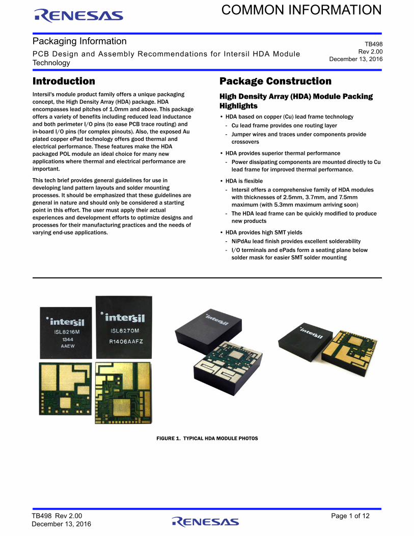
FIGURE 1. TYPICAL HDA MODULE PHOTOS
TB498 Rev 2.00 Page 1 of 12December 13, 2016
Packaging InformationPCB Design and Assembly Recommendations for
Intersil HDA Module Technology
FIGURE 2. TYPICAL HDA BOTTOM VIEW – ISL8270M
NOTE: All pads are non-solder mask defined and extend above the SM surface. The pad finish is NiPdAu for good solderability. The Au finish is 0.6µin thick to prevent gold embrittlement of the solder joint.
CONTROLLER LOCATION
INDUCTOR LOCATION
DrMOS LOCATION
Cu LEAD FRAME ROUTINGCOVERED BY SOLDER MASK
FIGURE 3. TYPICAL HDA MODULE X-RAY – ISL8270M
Cu LEAD FRAME ROUTING
CONTROLLER
DrMOS
INDUCTOR
VARIOUS CAPACITORSAND RESISTORS
TB498 Rev 2.00 Page 2 of 12December 13, 2016

Packaging InformationPCB Design and Assembly Recommendations for
Intersil HDA Module Technology
Moisture SensitivityMoisture Sensitivity Handling, Packing, and Use
MOISTURE SENSITIVITYIntersil HDA modules are moisture-sensitive devices. All Intersil HDA modules meet Moisture Sensitivity Level (MSL) 3 per J-STD-020.
Pb-free reflow is qualified per J-STD-020. Peak temperatures vary based on module thickness and volume, and are specified on the MSL label and at www.intersil.com.
PACKING AND LABELINGIntersil packs and labels HDA modules per J-STD-033. Standard packing is in JEDEC trays. Add a “-T” to the part number for tape and reel packing. For more information on tape and reel specifications for integrated circuits, see tech brief TB347.
HANDLING AND USECustomers should handle and use HDA modules per J-STD-033. The modules are MSL 3 qualified – do not exceed 168-hour floor life. If floor life is exceeded, bake at +125°C for 48 hours.
ReliabilityStandard HDA Module Development Flow and QualificationPrior to the package and/or product builds for qualification (design phase), discrete component reliability reports are reviewed and approved. The Intersil Corporate Process Reliability group tests and/or approves process technology wear-out data (i.e., TDDB, Hot Carrier, HTRB, EM, etc.) to ensure the process technology for embedded controllers, power FETs, power stage, etc., meet the Intersil wear-out goals.
The package engineering group executes “look-ahead” evaluations to ensure the package is robust and meets design goals. Once the design phase is complete, the HDA power module and package moves into the Product/Package Reliability qualification phase.
Typical Reliability Qualification Stress Tests• MSL Test – Determines Moisture Sensitivity Level per
J-STD-020.
• Precondition Stress – Samples for BHAST, UHAST, THB, and TMCL are preconditioned. Stress includes moisture soak per MSL and three-time reflow cycles at the Pb-free peak reflow temperature, per J-STD-020.
• BHAST or THB – Static bias in a moisture-rich environment. Stress targets possible electrolytic related failure mechanisms. Typical stress runs for 96 hours or 1000 hours, respectively.
• High Temperature Operating Life (HTOL) – Dynamic operation, maximum operating voltage per datasheet. This stress test is used to verify the long term reliability of the module. Data is used to calculate FIT rate and MTTF. Typical stress runs for 1000 hours with module temperature set at +125°C.
• Temperature Cycling (TMCL) – This stress test targets flaws in the thermo-mechanical properties of the module design or BOM. Typical stress includes 500 cycles at -65°C/+150°C or 1000 cycles at -40°C/+125°C.
• High Temperature Storage Life (HTSL) – This stress test is used as an indicator of thermally activated failure mechanisms. Typical stress runs for 1000 hours at 150°C.
• Unbiased HAST (UHAST) – This stress test accelerates the penetration of moisture through a protective mold compound and is used to identify failure mechanisms internal to the package, such as galvanic corrosion. Typical stress runs for 96 hours at +130°C/85% RH, 2ATM pressure.
• Reliability reports available on www.intersil.com/support
FIGURE 4. TYPICAL HDA MODULE CROSS-SECTION
WIRE BONDS
CONTROLLER - QFNINDUCTOR
DIER/C
Sn/Sb SOLDER
Cu ALLOY LEADFRAME WITHNiPdAu TERMINATION FINISH
SOLDER MASKI/O PAD
MOLD COMPOUND
ePad
I/O PADS AND ePadsFORM SEATING PLANE
TB498 Rev 2.00 Page 3 of 12December 13, 2016

Packaging InformationPCB Design and Assembly Recommendations for
Intersil HDA Module Technology
Intersil HDA Power Module – Board Level ReliabilityIntersil verifies the BLR of HDA modules by:
• Mounting functional modules or daisy chain modules on PCBs
• Using SAC 305 or SnPb solder
• Performing temperature cycles of –40°C to +125°C, 12-minute dwell (typical)
• Running 2000 cycles (typical)
• Conducting down point and end point electrical tests to confirm module functionality or no resistance change
• Testing end point cross section to confirm no solder joint damage
A summary of BLR data is available at www.intersil.com. Detailed reports are also available. Contact Intersil Sales to request a detailed BLR report.
PCB Design GuidelinesHDA – PCB Design Guidelines• The Intersil HDA package outline drawing in the product
datasheet includes a PCB footprint and solder stencil
• PCB lands in the form of SMD pads are preferred to improve gasketing
• PCB lands should match the HDA pads one-to-one
• Large ePads should be “windowpaned” with SM
- The SM webs provide gasketing to improve solder release during printing, control solder spread/thickness, and provide venting for out-gassing during reflow
- See the Package Outline Drawing (POD) for specific design recommendations
• Solder stencil apertures should be slightly smaller than the solder mask openings, 30µm typical.
• Via in pad should be filled and plated over (VIPPO) to prevent solder wicking into the vias.
• Electroless Nickel Immersion Gold (ENIG) PCB finish recommended
PCB Assembly ProcessHDA – PCB Assembly Process• Profile with a thermal couple placed under the HDA module
• Follow solder paste supplier’s reflow profile, but do not exceed HDA module’s qualified peak reflow temp. Pb-free reflow is qualified per J-STD-020:
- Peak temperature varies based on module thickness and volume
- Peak temperature specified on MSL label or www.intersil.com
• Do not exceed 168-hour out of bag limit (MSL 3 qualified)
- If time limit exceeded bake per MSL label instructions
• Solder foil preforms may be used on large ePads to reduce solder voids and flux residue and to increase stand-off height
• Use the following assembly tooling materials for the SMT process:
- Electroless Nickel Immersion Gold PCB finish (ENIG)
- Stainless steel, laser cut stencils with Nano-coating
- 4 mil or 5 mil stencil thickness
- No clean, low void, Type 3 or 4 solder paste per ANSI/J-STD-005
• Follow paste suppliers recommendation for air or nitrogen purge during reflow
• Solder Print Inspection (SPI) is recommended to ensure consistent solder deposit area, height, and volume
FIGURE 5. TYPICAL HDA MODULE PHOTOS
MODULE BOTTOM VIEW
PCB TOP VIEW
SOLDER MASK WINDOW PANES ON LARGE ePads
SIZE OF PCB LANDS MATCH MODULE PADS
TB498 Rev 2.00 Page 4 of 12December 13, 2016

Packaging InformationPCB Design and Assembly Recommendations for
Intersil HDA Module Technology
ISL8272M/ISL8273M Validated SMT Process SummaryTABLE 1. SCREEN PRINT
MACHINE MATERIALS
Screen Printer DEK Horizon O2i Solder Paste Alpha CVP-390 SAC 305
Pressure 8Kg Thawing Time 4 hrs
Speed 15mm/sec Auto Mix Time 3 min
Single/Dual Print Single TOOLING
Separate Speed 0.3mm/sec Stencil Thickness 5 mils
Separate Distance 2mm Stencil Opening Per POD
Printing Gap 0mm Stencil Made Laser cut + electro polishing
TABLE 2. COMPONENT PLACEMENT
MACHINE MATERIALS
Chip Shooter Yamaha YG100G Components Intersil 8272M Modules
Pick-up Speed 30% Packing JEDEC Tray
Place Speed 30% Pre-Bake NO
Transport Speed 50% TOOLING
Place Height 0.2mm Feeder Tray Loader
Vacuum Level 30% Nozzle 214
TB498 Rev 2.00 Page 5 of 12December 13, 2016

Packaging InformationPCB Design and Assembly Recommendations for
Intersil HDA Module Technology
STATISTIC NAME LOW LIMIT HIGH LIMIT UNITS
Max Rising Slope (Target = 1.0) (calculate slope over 30 seconds)
0.7 1.3 Degrees/Second
Max Falling Slope(calculate slope over 30 seconds)
-6.0 -1.0 Degrees/Second
Soak Time +155°C to +175°C 60 100 Seconds
Time Above Reflow -217°C 60 90 Seconds
Peak Temperature 235 245 °C
TB498 Rev 2.00 Page 6 of 12December 13, 2016
Packaging InformationPCB Design and Assembly Recommendations for
Intersil HDA Module Technology
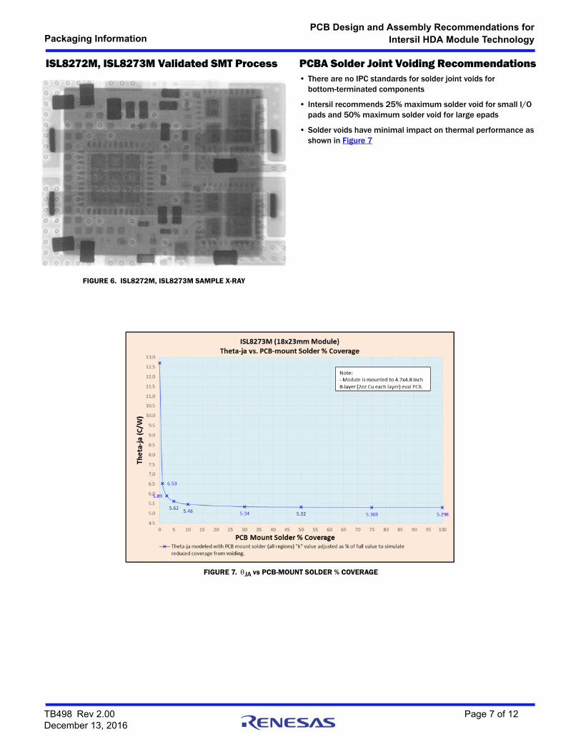
ISL8272M, ISL8273M Validated SMT Process PCBA Solder Joint Voiding Recommendations• There are no IPC standards for solder joint voids for
bottom-terminated components
• Intersil recommends 25% maximum solder void for small I/O pads and 50% maximum solder void for large epads
• Solder voids have minimal impact on thermal performance as shown in Figure 7
FIGURE 6. ISL8272M, ISL8273M SAMPLE X-RAY
FIGURE 7. JA vs PCB-MOUNT SOLDER % COVERAGE
TB498 Rev 2.00 Page 7 of 12December 13, 2016
Packaging InformationPCB Design and Assembly Recommendations for
Intersil HDA Module Technology
PCBA ReworkFor rework of defects underneath the package, the whole package needs to be removed.
Removal and rework of HDAs should be done on a rework station with thermal profile control (see Figure 8). The following steps are provided as a guideline – a starting point in developing a successful rework process.
BakeBefore rework, bake the PCB assembly at +125°C for at least 48 hours to remove any residual moisture.
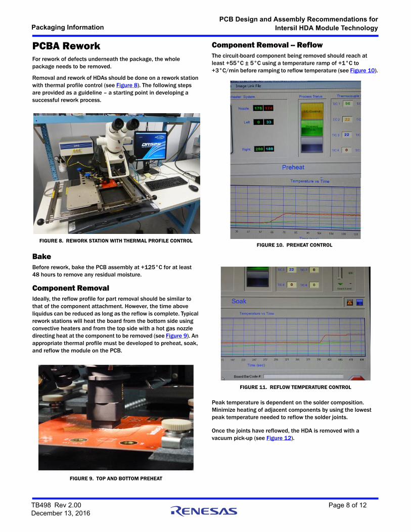
Component RemovalIdeally, the reflow profile for part removal should be similar to that of the component attachment. However, the time above liquidus can be reduced as long as the reflow is complete. Typical rework stations will heat the board from the bottom side using convective heaters and from the top side with a hot gas nozzle directing heat at the component to be removed (see Figure 9). An appropriate thermal profile must be developed to preheat, soak, and reflow the module on the PCB.
Component Removal -- ReflowThe circuit-board component being removed should reach at least +55°C ± 5°C using a temperature ramp of +1°C to +3°C/min before ramping to reflow temperature (see Figure 10).
Peak temperature is dependent on the solder composition. Minimize heating of adjacent components by using the lowest peak temperature needed to reflow the solder joints.
Once the joints have reflowed, the HDA is removed with a vacuum pick-up (see Figure 12).
FIGURE 8. REWORK STATION WITH THERMAL PROFILE CONTROL
FIGURE 9. TOP AND BOTTOM PREHEAT
FIGURE 10. PREHEAT CONTROL
FIGURE 11. REFLOW TEMPERATURE CONTROL
TB498 Rev 2.00 Page 8 of 12December 13, 2016
Packaging InformationPCB Design and Assembly Recommendations for
Intersil HDA Module Technology
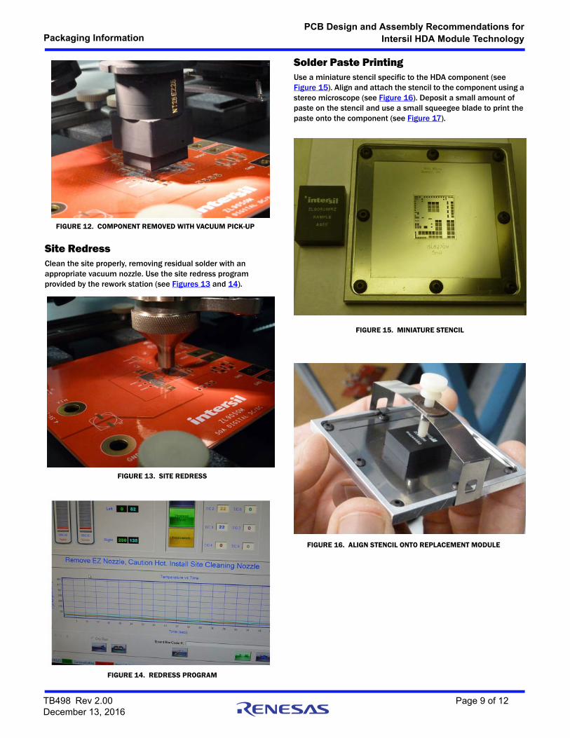
Site RedressClean the site properly, removing residual solder with an appropriate vacuum nozzle. Use the site redress program provided by the rework station (see Figures 13 and 14).
Solder Paste PrintingUse a miniature stencil specific to the HDA component (see Figure 15). Align and attach the stencil to the component using a stereo microscope (see Figure 16). Deposit a small amount of paste on the stencil and use a small squeegee blade to print the paste onto the component (see Figure 17).
FIGURE 12. COMPONENT REMOVED WITH VACUUM PICK-UP
FIGURE 13. SITE REDRESS
FIGURE 14. REDRESS PROGRAM
FIGURE 15. MINIATURE STENCIL
FIGURE 16. ALIGN STENCIL ONTO REPLACEMENT MODULE
TB498 Rev 2.00 Page 9 of 12December 13, 2016

Packaging InformationPCB Design and Assembly Recommendations for
Intersil HDA Module Technology
Component Alignment and PlacementCarefully place the HDA module in the pick-up position (see Figure 18).
Use the rework station’s optical system overlay and align the images of the HDA terminals with the printed solder and PCB land pattern (see Figure 19).
Component ReflowReflow the component using the same reflow profile as originally developed for the PCBA based on the solder paste used (see Figure 20). The rework is completed (see Figure 21).
FIGURE 17. DEPOSIT PASTE WITH SMALL SQUEEGEE BLADE
FIGURE 18. PLACEMENT OF NEW DEVICE
FIGURE 19. OVERLAY IMAGE ALIGNMENT
FIGURE 20. COMPONENT PLACEMENT
FIGURE 21. COMPLETED REWORK
TB498 Rev 2.00 Page 10 of 12December 13, 2016
Packaging InformationPCB Design and Assembly Recommendations for
Intersil HDA Module Technology
Questions and Answers• What is HDA?
- High Density Array (HDA) is a unique, Intersil developed, module packaging technology based on a routable, copper (Cu) lead frame construction, which provides superior thermal performance compared to laminate substrate based modules.
• Can HDA modules be reworked?
- Yes, a rework station used for BGA rework is recommended. See “PCBA Rework” on page 8.
• Can HDA modules be mounted on the bottom side of the PCBA?
- HDAs with a maximum thickness of 2.5mm and 3.7mm may be mounted on the PCBA bottom side. HDAs with 5.3mm and 7.5mm maximum thickness are not recommended for bottom side mounting.
• What is the maximum amount of solder voiding allowed?
- See discussion in “PCBA Solder Joint Voiding Recommendations” on page 7.
TB498 Rev 2.00 Page 11 of 12December 13, 2016
http://www.renesas.comRefer to "http://www.renesas.com/" for the latest and detailed information.
Renesas Electronics America Inc.1001 Murphy Ranch Road, Milpitas, CA 95035, U.S.A.Tel: +1-408-432-8888, Fax: +1-408-434-5351Renesas Electronics Canada Limited9251 Yonge Street, Suite 8309 Richmond Hill, Ontario Canada L4C 9T3Tel: +1-905-237-2004Renesas Electronics Europe LimitedDukes Meadow, Millboard Road, Bourne End, Buckinghamshire, SL8 5FH, U.KTel: +44-1628-651-700, Fax: +44-1628-651-804Renesas Electronics Europe GmbHArcadiastrasse 10, 40472 Düsseldorf, Germany Tel: +49-211-6503-0, Fax: +49-211-6503-1327Renesas Electronics (China) Co., Ltd.Room 1709 Quantum Plaza, No.27 ZhichunLu, Haidian District, Beijing, 100191 P. R. ChinaTel: +86-10-8235-1155, Fax: +86-10-8235-7679Renesas Electronics (Shanghai) Co., Ltd.Unit 301, Tower A, Central Towers, 555 Langao Road, Putuo District, Shanghai, 200333 P. R. China Tel: +86-21-2226-0888, Fax: +86-21-2226-0999Renesas Electronics Hong Kong LimitedUnit 1601-1611, 16/F., Tower 2, Grand Century Place, 193 Prince Edward Road West, Mongkok, Kowloon, Hong KongTel: +852-2265-6688, Fax: +852 2886-9022Renesas Electronics Taiwan Co., Ltd.13F, No. 363, Fu Shing North Road, Taipei 10543, TaiwanTel: +886-2-8175-9600, Fax: +886 2-8175-9670Renesas Electronics Singapore Pte. Ltd.80 Bendemeer Road, Unit #06-02 Hyflux Innovation Centre, Singapore 339949Tel: +65-6213-0200, Fax: +65-6213-0300Renesas Electronics Malaysia Sdn.Bhd.Unit 1207, Block B, Menara Amcorp, Amcorp Trade Centre, No. 18, Jln Persiaran Barat, 46050 Petaling Jaya, Selangor Darul Ehsan, MalaysiaTel: +60-3-7955-9390, Fax: +60-3-7955-9510Renesas Electronics India Pvt. Ltd.No.777C, 100 Feet Road, HAL 2nd Stage, Indiranagar, Bangalore 560 038, IndiaTel: +91-80-67208700, Fax: +91-80-67208777Renesas Electronics Korea Co., Ltd.17F, KAMCO Yangjae Tower, 262, Gangnam-daero, Gangnam-gu, Seoul, 06265 KoreaTel: +82-2-558-3737, Fax: +82-2-558-5338
SALES OFFICES
© 2018 Renesas Electronics Corporation. All rights reserved.Colophon 7.0
(Rev.4.0-1 November 2017)
Notice
1. Descriptions of circuits, software and other related information in this document are provided only to illustrate the operation of semiconductor products and application examples. You are fully responsible for
the incorporation or any other use of the circuits, software, and information in the design of your product or system. Renesas Electronics disclaims any and all liability for any losses and damages incurred by
you or third parties arising from the use of these circuits, software, or information.
2. Renesas Electronics hereby expressly disclaims any warranties against and liability for infringement or any other claims involving patents, copyrights, or other intellectual property rights of third parties, by or
arising from the use of Renesas Electronics products or technical information described in this document, including but not limited to, the product data, drawings, charts, programs, algorithms, and application
examples.
3. No license, express, implied or otherwise, is granted hereby under any patents, copyrights or other intellectual property rights of Renesas Electronics or others.
4. You shall not alter, modify, copy, or reverse engineer any Renesas Electronics product, whether in whole or in part. Renesas Electronics disclaims any and all liability for any losses or damages incurred by
you or third parties arising from such alteration, modification, copying or reverse engineering.
5. Renesas Electronics products are classified according to the following two quality grades: “Standard” and “High Quality”. The intended applications for each Renesas Electronics product depends on the
product’s quality grade, as indicated below.
"Standard": Computers; office equipment; communications equipment; test and measurement equipment; audio and visual equipment; home electronic appliances; machine tools; personal electronic
equipment; industrial robots; etc.
"High Quality": Transportation equipment (automobiles, trains, ships, etc.); traffic control (traffic lights); large-scale communication equipment; key financial terminal systems; safety control equipment; etc.
Unless expressly designated as a high reliability product or a product for harsh environments in a Renesas Electronics data sheet or other Renesas Electronics document, Renesas Electronics products are
not intended or authorized for use in products or systems that may pose a direct threat to human life or bodily injury (artificial life support devices or systems; surgical implantations; etc.), or may cause
serious property damage (space system; undersea repeaters; nuclear power control systems; aircraft control systems; key plant systems; military equipment; etc.). Renesas Electronics disclaims any and all
liability for any damages or losses incurred by you or any third parties arising from the use of any Renesas Electronics product that is inconsistent with any Renesas Electronics data sheet, user’s manual or
other Renesas Electronics document.
6. When using Renesas Electronics products, refer to the latest product information (data sheets, user’s manuals, application notes, “General Notes for Handling and Using Semiconductor Devices” in the
reliability handbook, etc.), and ensure that usage conditions are within the ranges specified by Renesas Electronics with respect to maximum ratings, operating power supply voltage range, heat dissipation
characteristics, installation, etc. Renesas Electronics disclaims any and all liability for any malfunctions, failure or accident arising out of the use of Renesas Electronics products outside of such specified
ranges.
7. Although Renesas Electronics endeavors to improve the quality and reliability of Renesas Electronics products, semiconductor products have specific characteristics, such as the occurrence of failure at a
certain rate and malfunctions under certain use conditions. Unless designated as a high reliability product or a product for harsh environments in a Renesas Electronics data sheet or other Renesas
Electronics document, Renesas Electronics products are not subject to radiation resistance design. You are responsible for implementing safety measures to guard against the possibility of bodily injury, injury
or damage caused by fire, and/or danger to the public in the event of a failure or malfunction of Renesas Electronics products, such as safety design for hardware and software, including but not limited to
redundancy, fire control and malfunction prevention, appropriate treatment for aging degradation or any other appropriate measures. Because the evaluation of microcomputer software alone is very difficult
and impractical, you are responsible for evaluating the safety of the final products or systems manufactured by you.
8. Please contact a Renesas Electronics sales office for details as to environmental matters such as the environmental compatibility of each Renesas Electronics product. You are responsible for carefully and
sufficiently investigating applicable laws and regulations that regulate the inclusion or use of controlled substances, including without limitation, the EU RoHS Directive, and using Renesas Electronics
products in compliance with all these applicable laws and regulations. Renesas Electronics disclaims any and all liability for damages or losses occurring as a result of your noncompliance with applicable
laws and regulations.
9. Renesas Electronics products and technologies shall not be used for or incorporated into any products or systems whose manufacture, use, or sale is prohibited under any applicable domestic or foreign laws
or regulations. You shall comply with any applicable export control laws and regulations promulgated and administered by the governments of any countries asserting jurisdiction over the parties or
transactions.
10. It is the responsibility of the buyer or distributor of Renesas Electronics products, or any other party who distributes, disposes of, or otherwise sells or transfers the product to a third party, to notify such third
party in advance of the contents and conditions set forth in this document.
11. This document shall not be reprinted, reproduced or duplicated in any form, in whole or in part, without prior written consent of Renesas Electronics.
12. Please contact a Renesas Electronics sales office if you have any questions regarding the information contained in this document or Renesas Electronics products.
(Note 1) “Renesas Electronics” as used in this document means Renesas Electronics Corporation and also includes its directly or indirectly controlled subsidiaries.
(Note 2) “Renesas Electronics product(s)” means any product developed or manufactured by or for Renesas Electronics.