tcan455x clock optimization and design guidelines
TRANSCRIPT

Application ReportTCAN455x Clock Optimization and Design Guidelines
Jonathan Nerger
ABSTRACT
The TCAN455x family of devices are Controller Area Network Flexible Data Rate (CAN FD) controllers with integrated transceivers and a SPI interface. A 20 MHz or 40 MHz clock is required with either a crystal resonator placed between the OSC1 and OSC2 pins, or a single-ended clock input from the microprocessor or some other clock source can be supplied to the OSC1 pin while the OSC2 pin is grounded. Due to the support of both types of clock inputs, when a crystal resonator is used, some extra care must be taken to optimize the circuit components to guarantee stable operation. This application report discusses the crystal resonator optimization procedures, but assumes the reader has some basic understanding of crystal oscillators.
Table of Contents1 Introduction.............................................................................................................................................................................22 Crystal Oscillator Oscillation Concept................................................................................................................................. 33 TCAN455x Clock Structure.................................................................................................................................................... 44 Calculate the Load Capacitance............................................................................................................................................65 Measure the Oscillation Frequency...................................................................................................................................... 76 Calculate the Load Resistance..............................................................................................................................................97 Calculate the Negative Resistance..................................................................................................................................... 108 Evaluate the Crystal for Margin........................................................................................................................................... 119 Calculate the Startup Time and Quality Factor.................................................................................................................. 1110 Calculate the Drive Level................................................................................................................................................... 1211 Calculate the External Dampening Resistor.................................................................................................................... 1512 Recalculate Critical Transconductance and Gain Margin...............................................................................................1513 Verify and Check for Margin.............................................................................................................................................. 1514 Summary............................................................................................................................................................................. 16
List of FiguresFigure 1-1. TCAN455x Clock Simplified Block Diagram..............................................................................................................2Figure 2-1. Oscillator Model.........................................................................................................................................................3Figure 2-2. Cyrstal Oscillator Model............................................................................................................................................ 3Figure 3-1. TCAN455x Pierce Oscillator Simplified Circuit Representations...............................................................................5Figure 4-1. Crystal Load Capacitance......................................................................................................................................... 6Figure 5-1. Oscillation Frequency Test Setup..............................................................................................................................7Figure 6-1. Quarts Crystal Electrical Model................................................................................................................................. 9Figure 7-1. Negative Resistance Measurement Test Setup...................................................................................................... 10Figure 10-1. Drive Level Measurement Test Setup with Current Probe.................................................................................... 12Figure 10-2. Drive Level Measurement Test Setup with Differential FET Probe........................................................................13Figure 10-3. Drive Level Measurement Test Setup with Single-Ended FET Probe................................................................... 14
TrademarksAll trademarks are the property of their respective owners.
www.ti.com Table of Contents
SLLA549 – JULY 2021Submit Document Feedback
TCAN455x Clock Optimization and Design Guidelines 1
Copyright © 2021 Texas Instruments Incorporated
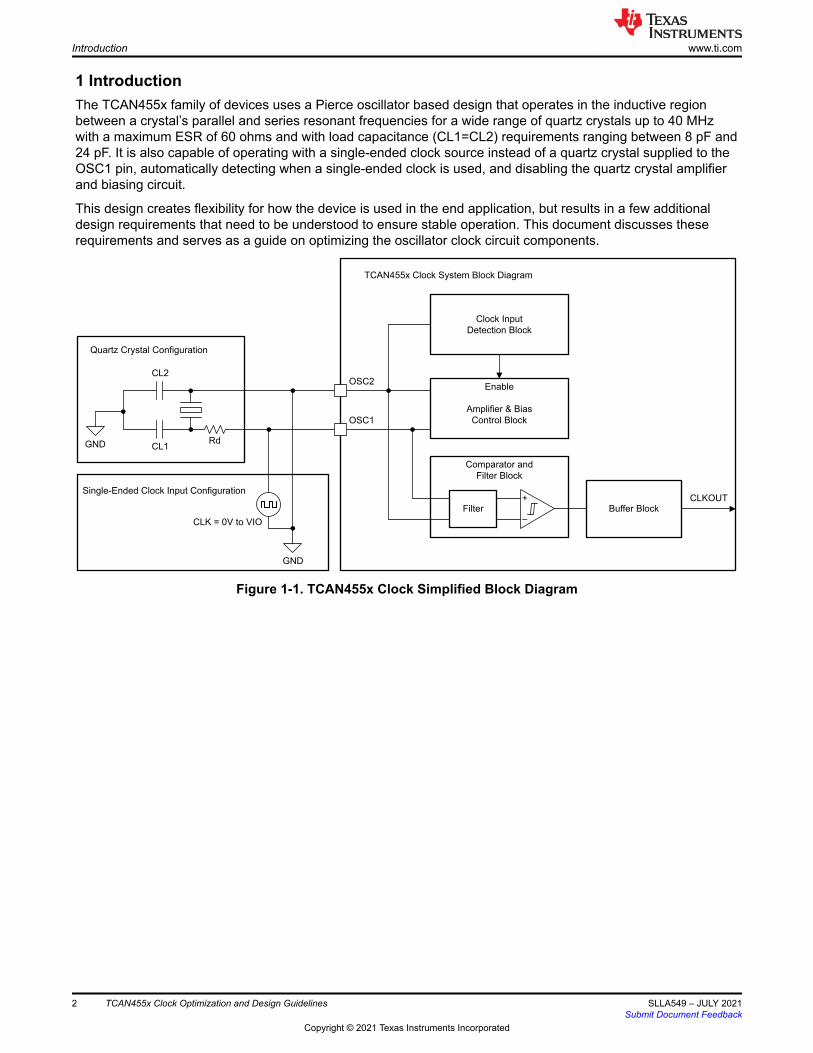
1 IntroductionThe TCAN455x family of devices uses a Pierce oscillator based design that operates in the inductive region between a crystal’s parallel and series resonant frequencies for a wide range of quartz crystals up to 40 MHz with a maximum ESR of 60 ohms and with load capacitance (CL1=CL2) requirements ranging between 8 pF and 24 pF. It is also capable of operating with a single-ended clock source instead of a quartz crystal supplied to the OSC1 pin, automatically detecting when a single-ended clock is used, and disabling the quartz crystal amplifier and biasing circuit.
This design creates flexibility for how the device is used in the end application, but results in a few additional design requirements that need to be understood to ensure stable operation. This document discusses these requirements and serves as a guide on optimizing the oscillator clock circuit components.
Clock Input
Detection Block
Enable
Amplifier & Bias
Control Block
Comparator and
Filter Block
Filter+
–Buffer Block
GND RdCL1
CL2
Quartz Crystal Configuration
TCAN455x Clock System Block Diagram
OSC2
OSC1
GND
Single-Ended Clock Input Configuration
CLK = 0V to VIO
CLKOUT
Figure 1-1. TCAN455x Clock Simplified Block Diagram
Introduction www.ti.com
2 TCAN455x Clock Optimization and Design Guidelines SLLA549 – JULY 2021Submit Document Feedback
Copyright © 2021 Texas Instruments Incorporated
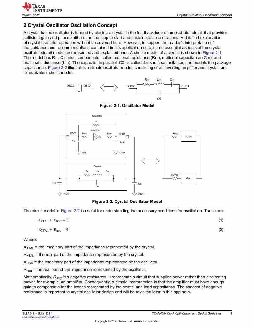
2 Crystal Oscillator Oscillation ConceptA crystal-based oscillator is formed by placing a crystal in the feedback loop of an oscillator circuit that provides sufficient gain and phase shift around the loop to start and sustain stable oscillations. A detailed explanation of crystal oscillator operation will not be covered here. However, to support the reader’s interpretation of the guidance and recommendations contained in this application note, some essential aspects of the crystal oscillator circuit model are presented and explained here. A simple model of a crystal is shown in Figure 2-1. The model has R-L-C series components, called motional resistance (Rm), motional capacitance (Cm), and motional inductance (Lm). The capacitor in parallel, C0, is called the shunt capacitance, and models the package capacitance. Figure 2-2 illustrates a simple oscillator model, consisting of an inverting amplifier and crystal, and its equivalent circuit model.
Rm Cm
C0
Lm
OSC2 OSC1OSC2 OSC1
Figure 2-1. Oscillator Model
Rf
Resd
Rm Cm
C0
Lm
OSC1
Cin
Resd
Af
Cout
GND GND
Amplifier
OSC2
CL2 CL1
GND GND
Oscillator
Crystal
XOSC
XTAL
-Rneg
RXTAL
Figure 2-2. Cyrstal Oscillator Model
The circuit model in Figure 2-2 is useful for understanding the necessary conditions for oscillation. These are:XXTAL+ XOSC = 0 (1)RXTAL+ Rneg = 0 (2)
Where:
XXTAL = the imaginary part of the impedance represented by the crystal.
RXTAL = the real part of the impedance represented by the crystal.
XOSC = the imaginary part of the impedance represented by the oscillator.
Rneg = the real part of the impedance represented by the oscillator.
Mathematically, Rneg is a negative resistance. It represents a circuit that supplies power rather than dissipating power, for example, an amplifier. Consequently, a simple interpretation is that the amplifier must have enough gain to compensate for the losses represented by the crystal and load capacitance. The concept of negative resistance is important to crystal oscillator design and will be revisited later in this app note.
www.ti.com Crystal Oscillator Oscillation Concept
SLLA549 – JULY 2021Submit Document Feedback
TCAN455x Clock Optimization and Design Guidelines 3
Copyright © 2021 Texas Instruments Incorporated

3 TCAN455x Clock StructureThe TCAN455x clock circuit contains three main blocks, an Amplifier and Bias Control block, a Filter and Comparator block, and a Clock Input Detection block as shown in Figure 1-1. A Comparator is used to compare the voltage difference between the OSC1 and OSC2 pins and generate the Clock Output signal used by the device when either a quartz crystal or single-ended clock input is used. The positive input of the comparator is connected to the OSC1 pin, and the negative input is connected to the OSC2 pin. When a single-ended clock is used, the clock signal is applied to the positive input of the comparator through the OSC1 pin, and the negative input of the comparator is held low by connecting the OSC2 pin to ground.
The Amplifier and Bias Control block provides the source current needed to start and sustain the crystal oscillation through the OSC1 pin when a quartz crystal is used, but it must be disabled when a single-ended clock input is used instead of a crystal. This is handled by the Clock Input Detection block that monitors the voltage level on the OSC2 pin and disables the Amplifier block if the voltage is below the detection threshold which is typically between 90mV to 150mV, such as when the pin is connected to ground. If the OSC2 pin is not connected to ground, the current supplied by the Amplifier and Bias block through the crystal will ideally keep the minimum voltage level of the oscillation waveform above 400mV and includes a peak detector circuit that will sense the oscillation envelope formed by the voltage difference between the OSC1 and OSC2 pins.
The crystal oscillator transconductance amplifier adjusts the amplifier bias current to maintain a consistent and stable oscillation when the voltage amplitude of the OSC1 and OSC2 waveforms are nominally 1 Vpp for each of the individual OSC1 and OSC2 signals, or 2 Vpp between the differential OSC1 and OSC2 signal resulting from their 180° phase shift. However, the actual voltage levels will depend on the total load connected to the TCAN455x oscillator circuit.
When the total external load on the amplifier created by the reactance of the load capacitance and the crystal equivalent series resistance is too small, the amplifier's minimum output current may cause the oscillation voltage amplitude levels to become too large by allowing too much power to flow through the crystal. If the voltage amplitude on the OSC2 pin becomes too large, the minimum peak voltage level of the signal could drop below the single-ended clock input detection threshold causing the amplifier and bias block to become disabled and stop the oscillation. When the external load is configured properly, the amplifier will be able to adjust the bias current to maintain a smaller voltage amplitude level in the nominal range and ensure the single-ended clock detection circuit will not disable the amplifier and bias control block.
Establishing the proper balance in the oscillation circuit is critical to stable reliable operation, preventing mechanical damage to the crystal, and guarantee several other factors not previously discussed. Ensuring the frequency of oscillation and the gain in the transconductance amplifier has enough margin to create the negative resistance needed to reliably establish the crystal oscillation must also be considered when selecting the values of the components used in the circuit. The remainder of this document will discuss how to avoid unreliable operation and determine the proper component values needed to meet all parametric concerns through a combination of measurements and calculations.
Common schematic representations of the Basic Pierce Oscillator circuit are shown in the following figure with the key components identified.
TCAN455x Clock Structure www.ti.com
4 TCAN455x Clock Optimization and Design Guidelines SLLA549 – JULY 2021Submit Document Feedback
Copyright © 2021 Texas Instruments Incorporated

+
–
Rf
OSC1
Cin Cout
GND
OSC2
TCAN455x
CLKOUT
CL2 CL1
GND
RdCPCB_Stray
+
–
Rf
OSC1
Cin Cout
GND
OSC2
TCAN455x
CLKOUT
CL2 CL1
GND
RdCPCB_Stray
gm
GND
VIO
Figure 3-1. TCAN455x Pierce Oscillator Simplified Circuit Representations
www.ti.com TCAN455x Clock Structure
SLLA549 – JULY 2021Submit Document Feedback
TCAN455x Clock Optimization and Design Guidelines 5
Copyright © 2021 Texas Instruments Incorporated

4 Calculate the Load Capacitance
CL2
GND
CPCB_Stray
Cin
CL1
Cout
Quartz Crystal
CLoad
Figure 4-1. Crystal Load Capacitance
Without a TCAN455x device, crystal, and load capacitors mounted on the board, measure the parasitic capacitance between the crystal footprint pads. If series resistors are used, include those on the board when making the measurement. This becomes the PCB stray capacitance that will be used in calculations CPCB_Stray.
The TCAN455x OSC1 Output Pin Capacitance Cout is typically 10 pF
The TCAN455x OSC2 Input Pin Capacitance Cin is typically 9 pF
Calculate the load capacitance presented to the crystal by the following formula:
CLoad = Cin + CL2 × CL1 + CoutCin + CL2 + CL1 + Cout + CPCB_Stray (3)
Where the OSC1 pin capacitance Cout is in parallel with the CL1 external load capacitance since they are both with respect to ground on the amplifier output side of the crystal and therefore added together.CL1+ Cout (4)
Where the OSC2 pin capacitance Cin is in parallel with the CL2 external load capacitance since they are both with respect to ground on the amplifier input side of the crystal and therefore added together.Cin+ CL2 (5)
Where the capacitance on both sides of the crystal are in series with each other relative to the crystal due to the common connection through the ground plane. Therefore they are calculated as capacitance in series.Cin + CL2 × CL1 + CoutCin + CL2 + CL1 + Cout (6)
Where the parasitic capacitance of the PCB between the OSC1 and OSC2 pins is in parallel with the capacitance of the components and is therefore added to component capacitance.CPCB_Stray (7)
Adjust the value of the external capacitors CL1 and CL2 to achieve a total load capacitance CLoad of the recommended value specified in the crystal data sheet.
Calculate the Load Capacitance www.ti.com
6 TCAN455x Clock Optimization and Design Guidelines SLLA549 – JULY 2021Submit Document Feedback
Copyright © 2021 Texas Instruments Incorporated

5 Measure the Oscillation Frequency
Notes:
Dashed lines indicate alternate or less
preferred test configurations
The E-Field Probe should be isolated
and not make electrical contact with
the crystal and behave as an
antennae.
RF IN
RF Amplifier
Gain = 20db to 30dB
RF OUT
CH4CH1 CH2 CH3
Oscilloscope
kHz
MHz
Frequency Counter
IN
Spectrum Analyzer
RF IN
Rd
CL2
CL1
GND
GND
FET Probe Cin < 1pF
TCAN455x
OSC2
OSC1
GND
GND
VIO VSUP
VIO VSUP
E-Field Probe or
Isolated Coax Cable
Figure 5-1. Oscillation Frequency Test Setup
Check for the motional parameters C0, Cm, resonant frequency (fs) and ESR on the data sheet of the crystal manufacturer. Calculate the resonant frequency of the crystal and of the crystal with the load capacitance.
Where the resonant frequency and motional inductance of the crystal is:
fs = 12π × Lm × Cm Lm = 14π2 × fs × Cm (8)
Where the resonant frequency of the crystal and capacitive load is:
fl = fs × 1 + CmC0 + CLoad (9)
Because the oscillator frequency is determined by load capacitance which is a product of the crystal’s shunt capacitance C0, the crystal’s Motional capacitance Cm, and the load capacitance of the board and external capacitors CLoad, it will shift according to the following formula:
dFF = −Cm2 C0 + CLoad (10)
Measure the oscillation frequency using an E-Field probe, sometimes called either a sniffer probe or antennae probe, connected to a RF Amplifier to strengthen the signal detected by the oscillation of the crystal, and a Spectrum Analyzer or Frequency Counter to display the frequency of the signal detected. This method does not place a direct load on the oscillation circuit that will alter the frequency of oscillation through additional resistance or capacitance inserted into the circuit by a directly connected voltage probe.
If an E-Field probe is not available, one can be made by exposing the conductor on one end of a coax cable that will act as an antenna, insulating it with heat shrink tubing to prevent electrical contact with any components on the board, and placing the insulated conductor directly on top of the crystal. The shield of the coax cable
www.ti.com Measure the Oscillation Frequency
SLLA549 – JULY 2021Submit Document Feedback
TCAN455x Clock Optimization and Design Guidelines 7
Copyright © 2021 Texas Instruments Incorporated

should be electrically connected to a ground location near the crystal to improve the signal quality and provide a reference for the test equipment.
The signal detected will likely have low amplitude and may need to be amplified with an RF Amplifier for a more reliable measurement by the spectrum analyzer. The amplitude of the signal is not important and it simply needs to be large enough for the spectrum analyzer to measure the frequency.
Tune the spectrum analyzer with a center frequency at the nominal crystal frequency and with a fairly narrow span such as 100 kHz so that there is enough resolution to capture the oscillation signal and accurately measure the center frequency.
If a spectrum analyzer is not available, a High Resolution Frequency Counter with a minimum of 7 to 8 digits of precision may be used if the signal has enough amplitude and is free of enough noise to return an accurate frequency count.
An alternative measurement can be done with an oscilloscope through a very low capacitance and high impedance active probe. The probe will add an additional capacitive/resistive load on the circuit and will slightly alter the oscillation frequency. Less than 1pF of probe capacitance is needed to minimize the frequency shift caused by the probe.
Oscilloscope measurements may not have enough resolution to get a high precision measurement of the exact oscillation frequency. A more accurate measurement can be obtained by using a High Resolution Frequency Counter.
Verify the frequency of oscillation is within the required specification and adjust the external capacitors to shift the frequency if needed. Increasing the capacitance will lower the frequency, and likewise reducing the capacitors will increase the frequency.
Re-calculate the load capacitance if the external capacitor values have been adjusted.
Measure the Oscillation Frequency www.ti.com
8 TCAN455x Clock Optimization and Design Guidelines SLLA549 – JULY 2021Submit Document Feedback
Copyright © 2021 Texas Instruments Incorporated

6 Calculate the Load ResistanceRm Cm
C0
Lm
C0 = Shunt Capacitance
Cm = Motional Capacitance
Lm = Motional Inductance
Rm = Motional Resistance
Figure 6-1. Quarts Crystal Electrical Model
Identify the crystal's shunt capacitance C0 and motional resistance Rm from the crystal’s data sheet or ask the crystal vendor if this is not specified.
Some crystal data sheets specify the Rm as the crystal’s maximum Equivalent Series Resistance or ESR. Other crystal data sheets use the term ESR to specify the total load resistance under the specified Capacitive Load which is greater than the motional resistance of the crystal itself as defined in the next step.
Calculate the combined load of the series resistance in the crystal and the reactance of the capacitance placed on the oscillator circuit. This will be to total Load Resistance RLoad which is different than the crystal’s motional resistance Rm. Both are sometimes referred to as the ESR and therefore there can be great confusion about what the term ESR is referring to. In calculations and for clarity the term ESR will not be used in this document. The crystal’s motional resistance will be designated by Rm and the total Load resistance will be designated by RLoad.
RLoad = Rm × 1 + C0CLoad 2 Rm = RLoad1 + C0CLoad 2 (11)
If the Motional Resistance Rm of the crystal is unknown, this can be approximated by using the maximum ESR listed in the data sheet (for example, 50 ohms), but this may not be accurate and is only a rough estimation that will cause the results to be larger than the actual or typical value (for example, 20 ohms).
www.ti.com Calculate the Load Resistance
SLLA549 – JULY 2021Submit Document Feedback
TCAN455x Clock Optimization and Design Guidelines 9
Copyright © 2021 Texas Instruments Incorporated

7 Calculate the Negative Resistance
Notes:
Dashed lines indicate alternate or less
preferred test configurations
The E-Field Probe should be isolated
and not make electrical contact with
the crystal and behave as an
antennae.
RF IN
RF Amplifier
Gain = 20db to 30dB
RF OUT
CH4CH1 CH2 CH3
Oscilloscope
kHz
MHz
Frequency Counter
IN
Spectrum Analyzer
RF IN
Rd
CL2
CL1
GND
GND
TCAN455x
OSC2
OSC1
GND
GND
VIO VSUP
VIO VSUP
E-Field Probe or
Isolated Coax CableRs
Figure 7-1. Negative Resistance Measurement Test Setup
The typical transconductance (gm) of the TCAN455x Pierce Oscillator circuit is 6.6 mS
Calculate the negative resistance by the following formula:
Rneg_calc = − gmω2 × 2 × CLoad 2 (12)
Measure the negative resistance by inserting a series resistor (Rs) in between the crystal pin and the CL1 external load capacitor on the amplifier output (OSC1) side of the crystal. Monitor the crystal oscillation frequency and increase the resistor value until the oscillation stops. The total negative resistance is equal to the Load Resistance plus the added series resistance.
This requires the crystal to be removed from the PCB so that the resistor can be inserted, while maintaining the electrical connections with the other components with as little additional inductive, resistive, and capacitive impact as possible.
A cermet potentiometer, which is ceramic based and non-inductive, could be used instead of replacing the series resistors with discrete resistors of increasing value. However, the potentiometer chosen should have low capacitance so that the capacitive reactance does not alter the total load resistance and load capacitance of the circuit in a significant way. Once the oscillation stops, the resistance across the potentiometer can be measured.
The amount of negative resistance in the system can be calculated by the following formula:Rneg = RSeries+ RLoad (13)
Compare the previously calculated negative resistance that was calculated with the typical transconductance value gm, to the value calculated using the resistor measurement method. If the values do not match, adjustments may be needed to the transconductance (gm), frequency (fs), RLoad, or CLoad values. Check the RLoad and CLoad calculations for accuracy and solve for a more accurate transconductance value gm.
Calculate the Negative Resistance www.ti.com
10 TCAN455x Clock Optimization and Design Guidelines SLLA549 – JULY 2021Submit Document Feedback
Copyright © 2021 Texas Instruments Incorporated
It is important that there is enough negative resistance to overcome changes in the circuit as a result of component tolerance differences on key parameters and shifting values due to environmental conditions such as temperature and humidity. If there is not enough margin between the amount of negative resistance and the load resistance, there is a chance the oscillation in the circuit can stop or fail to start when power is applied to the circuit. Verify the magnitude of the negative resistance is 3 to 5 times larger than the Load Resistance by the following formula. This is commonly referred to as the Safety Factor.
RSafety = − RnegRLoad (14)
If the negative resistance margin is too low, the load resistance RLoad is too large for ensured safe operation of the oscillation circuit. The load capacitance may need to be adjusted by using larger external capacitor values in order to lower the total load resistance.
If the capacitors are adjusted to improve the negative resistance margin, the oscillation frequency will shift. Re-measure the oscillation frequency to ensure it is still within specification. Re-calculate the load capacitance and load resistance values that will be needed in other calculations.
If the external load capacitors cannot be adjusted to an appropriate level, then a crystal with more appropriate motional properties may be needed.
It is important to reduce the parasitic PCB capacitance CPCB_Stray as much as possible with proper layout techniques to allow greater margin and room for adjustment with different values of components.
8 Evaluate the Crystal for MarginIf a crystal with more appropriate motional properties is needed, it is possible to evaluate the compatibility of a crystal resonator with the oscillator based on the motional properties of the crystal.
The critical transconductance (gmcrit) is the minimum transconductance required by the oscillator to maintain a stable oscillation for a given crystal and load capacitance that can be calculated by the following formula:
gmcrit = 4 × Rload × ω2 × C0+ CL 2 (15)
Where: Rload = Rm × 1 + C0+ CLoad 2 and ω = 2πf (16)
The gain margin (Gainmargin) can then be calculated by the following formula and the resulting ratio should be greater than 5 to ensure there is enough margin to start and maintain oscillation.
Gainmargin = gmgmcrit (17)
9 Calculate the Startup Time and Quality FactorThe ability of the crystal to sustain oscillation can be determined by the Quality Factor (Q) which is the ratio of the initial stored energy and the amount of energy lost in one radian cycle of oscillation. A higher Q factor will have less energy loss and longer sustained oscillation before the resonation dies out. Calculate the Quality factor (Q) by the following formula:
Q = 2π × Fs × LmRm (18)
The time it takes the oscillations to start and stabilize is also of importance. Several factors such as the drive level, load resistance, and the magnitude of the closed loop gain can impact the startup time (τ) of the oscillations which can be calculated by the following formula:
τ = 2 × LmRLoad + Rneg (19)
www.ti.com Evaluate the Crystal for Margin
SLLA549 – JULY 2021Submit Document Feedback
TCAN455x Clock Optimization and Design Guidelines 11
Copyright © 2021 Texas Instruments Incorporated
10 Calculate the Drive Level
CH4CH1 CH2 CH3
Oscilloscope
Rd
CL2
CL1
GND
GND
TCAN455x
OSC2
OSC1
GND
GND
VIO VSUP
VIO VSUP
AC Current Probe
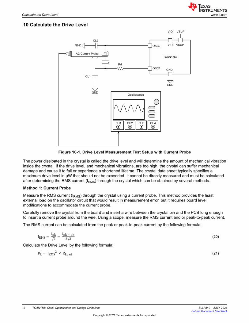
Figure 10-1. Drive Level Measurement Test Setup with Current Probe
The power dissipated in the crystal is called the drive level and will determine the amount of mechanical vibration inside the crystal. If the drive level, and mechanical vibrations, are too high, the crystal can suffer mechanical damage and cause it to fail or experience a shortened lifetime. The crystal data sheet typically specifies a maximum drive level in µW that should not be exceeded. It cannot be directly measured and must be calculated after determining the RMS current (IRMS) through the crystal which can be obtained by several methods.
Method 1: Current Probe
Measure the RMS current (IRMS) through the crystal using a current probe. This method provides the least external load on the oscillator circuit that would result in measurement error, but it requires board level modifications to accommodate the current probe.
Carefully remove the crystal from the board and insert a wire between the crystal pin and the PCB long enough to insert a current probe around the wire. Using a scope, measure the RMS current and or peak-to-peak current.
The RMS current can be calculated from the peak or peak-to-peak current by the following formula:
IRMS = Ipk2 = Ipk − pk2 2 (20)
Calculate the Drive Level by the following formula:DL = IRMS2 × RLoad (21)
Calculate the Drive Level www.ti.com
12 TCAN455x Clock Optimization and Design Guidelines SLLA549 – JULY 2021Submit Document Feedback
Copyright © 2021 Texas Instruments Incorporated

CH4CH1 CH2 CH3
Oscilloscope
Rd
CL2
CL1
GND
GND
TCAN455x
OSC2
OSC1
GND
GND
VIO VSUP
VIO VSUP
Differential FET Probe
Cin < 1pF
Figure 10-2. Drive Level Measurement Test Setup with Differential FET Probe
Method 2: Differential Active FET Probe
An alternative method is to calculate the IRMS current by measuring the voltage swing across the crystal with a differential active FET probe that has less than 1pF of capacitance. The probe capacitance will need to be factored into the calculation because it will add error to the measurement.
Measure the RMS voltage or peak-to-peak voltage across the crystal.
The RMS voltage can be calculated from the peak-to-peak voltage by the following formula:
VRMS = Vpp2 2 (22)
The RMS current can be calculated from the RMS voltage by the following formula:IRMS = VRMSR = VRMSXc = VRMS12πFc = 2πF × VRMS × Ctotal (23)
IRMS = 2πF × VRMS × Ctotal (24)Where: Ctotal = CLoad+ C0+ Cprobe (25)
The Drive Level (DL) can then be calculated by the following formula:
DL = π × F × Ctotal 2 × Vpp2 × RLoad2 (26)
If the Drive Level exceeds the maximum level specified by the crystal manufacturer, the total load capacitance may need to be adjusted to reduce RLoad, or an external series dampening resistor (Rd) needs to be added between the amplifier output and the crystal + CL1 net.
www.ti.com Calculate the Drive Level
SLLA549 – JULY 2021Submit Document Feedback
TCAN455x Clock Optimization and Design Guidelines 13
Copyright © 2021 Texas Instruments Incorporated

CH4CH1 CH2 CH3
Oscilloscope
Rd
CL1
GND
GND
TCAN455x
OSC2
OSC1
GND
GND
VIO VSUP
VIO VSUP
FET
Pro
be C
in <
1pF
CL2
Figure 10-3. Drive Level Measurement Test Setup with Single-Ended FET Probe
Method 3: Single-ended Active FET Probe
Another alternative method is to calculate the IRMS current by measuring the voltage swing at the input to the amplifier with an active FET probe that has less than 1pF of capacitance. The probe capacitance will need to be factored into the calculation because it will add error to the measurement. Measure the RMS voltage or peak-to-peak voltage across the CL2 capacitor on the amplifier input side of the crystal. The current flowing through this capacitor is approximately equal to the current flowing through the crystal with only a negligible amount flowing into the amplifier which can usually be neglected.
The RMS voltage can be calculated from the peak-to-peak voltage by the following formula:
VRMS = Vpp2 2 (27)
The RMS current can be calculated from the RMS voltage by the following formula:IRMS = VRMSR = VRMSXc = VRMS12πFc = 2πF × VRMS × Ctotal (28)
IRMS = 2πF × VRMS × Ctotal (29)Where: Ctotal = CL2+ CPCB_Stray2 + CprobeThe Drive Level can then be calculated by the following formula:
DL = π × F × Ctotal 2 × Vpp2 × RLoad2 (30)
If the drive level exceeds the maximum level specified by the crystal manufacturer, the total load capacitance may need to be adjusted to reduce RLoad, or an external series dampening resistor (Rd) needs to be added between the amplifier output and the crystal + CL1 net.
It is recommended to keep the load capacitance within the crystal manufacturer’s recommendation. However with lower load capacitors, the OSC2 swing can be too close to ground. This could trigger the CLKIN detection
Calculate the Drive Level www.ti.com
14 TCAN455x Clock Optimization and Design Guidelines SLLA549 – JULY 2021Submit Document Feedback
Copyright © 2021 Texas Instruments Incorporated

circuit that disables the oscillator and stops the oscillations. To avoid the CLKIN detection circuit disabling the oscillator, the load capacitance needs to increase resulting in lower drive levels as well, or a dampening resistor (Rd) needs to be added between the amplifier output and the crystal + CL1 net. This allows lower drive levels to be achieved without increasing the load capacitance beyond the recommended value.
11 Calculate the External Dampening ResistorThe dampening resistor Rd placed between the OSC1 pin of TCAN455x and the crystal along with the capacitor CL1 will help attenuate the Vpp level. The dampening series resistance Rd will limit the current and lower the voltage amplitude of the oscillation waveform by forming a voltage divider with the CL1 capacitor further reducing the power dissipated across the crystal and keeping the voltage on the OSC2 pin above the clock input detection threshold needed to prevent the Amplifier and Bias Control block from being disabled. The reactance of the CL1 capacitor can be calculated by following formula:
Xc = 12πFCL1 (31)
In a typical application using FR-4 PCB material contributing 2-3 pF of stray parasitic capacitance, and a crystal with an 8 pF load capacitance specification, this resistance Rd is typically in the range of 50 to 100 ohms and CL1 as low as 1 pF or 2.2 pF should be sufficient to ensure that OSC2 pin swings above the clock input detection threshold.
This dampening series resistance will be added to the load resistance seen by the oscillator and reduce the negative resistance margin. Recalculate the negative resistance margin with this additional series resistance to determine if there is still enough safety margin and that the magnitude of the negative resistance is still 3 to 5 times greater than the load resistance + Rs with the following formula:
Rneg = gmω2 × 2 × CLoad 2 − Rd (32)
Ensure that this does not exceed the negative resistance margin available. If the margin is too small, then the dampening series resistor may need to be reduced to a value that satisfies both the safety margin and drive level requirements. If this cannot be done, then larger load capacitors, a crystal with a lower motional resistance, and or a higher drive level specification must be used.
12 Recalculate Critical Transconductance and Gain MarginIf a series dampening resistor is used, the critical transconductance gmcrit and gain margin needs to be recalculated to ensure there is still enough gain margin to start and maintain oscillation.
gmcrit_with_Rd = 4 × Rload+ Rd × ω2 × C0+ CL 2 (33)
Gainmargin_with_Rd = gmgmcrit_with_Rd (34)
13 Verify and Check for MarginRe-check the frequency, Drive Level and negative resistance if any components have been modified in the process and repeat until all requirements have been satisfied.
Calculate the temperature derating coefficient’s impact on the circuit, including component tolerances of all resistors and capacitors in the circuit. Recalculate the values with the min/max and derated values.
Test the development board over the desired temperature and voltage range to verify there is no undesired behavior such as an excessive frequency shift, or the crystal fails to start or stops oscillating during operation. The parasitic capacitance is not typically stable across temperature and the total CLoad will tend to vary slightly with temperature.
If issues are detected, adjust the capacitance and series dampening resistance and re-evaluate the frequency, negative resistance, Drive Level, and voltage level parameters as necessary.
www.ti.com Calculate the External Dampening Resistor
SLLA549 – JULY 2021Submit Document Feedback
TCAN455x Clock Optimization and Design Guidelines 15
Copyright © 2021 Texas Instruments Incorporated

14 SummaryAs described, the dual crystal oscillator and single-ended input clock structure of the TCAN455x poses additional design requirements with regards to the component selection used in this circuit. It is common to see a crystal oscillator circuit that contains only a crystal and two external load capacitors but does not contain a series damping resistor. Omitting the series dampening resistor Rd may or may not be acceptable and increases the risk of causing the clock to stop, fail to start, or overdrive the crystal with excessive power reducing its lifetime due to mechanical stress and increasing the oscillation Vpp amplitude to unacceptable levels.
Relying solely on external load capacitors large enough to keep the oscillation Vpp amplitude away from the single ended clock input detection threshold is possible, but this could result in a small frequency shift if the total load capacitance seen by the crystal exceeds its typical specification
Therefore, it is recommended to add a series damping resistor into the design to limit the oscillation Vpp amplitude without requiring excessive load capacitance. By adding this extra series resistor and taking the time to determine the proper value for all components in the circuit, many problems can be avoided resulting in a reliable and stable circuit design.
Summary www.ti.com
16 TCAN455x Clock Optimization and Design Guidelines SLLA549 – JULY 2021Submit Document Feedback
Copyright © 2021 Texas Instruments Incorporated

IMPORTANT NOTICE AND DISCLAIMERTI PROVIDES TECHNICAL AND RELIABILITY DATA (INCLUDING DATASHEETS), DESIGN RESOURCES (INCLUDING REFERENCEDESIGNS), APPLICATION OR OTHER DESIGN ADVICE, WEB TOOLS, SAFETY INFORMATION, AND OTHER RESOURCES “AS IS”AND WITH ALL FAULTS, AND DISCLAIMS ALL WARRANTIES, EXPRESS AND IMPLIED, INCLUDING WITHOUT LIMITATION ANYIMPLIED WARRANTIES OF MERCHANTABILITY, FITNESS FOR A PARTICULAR PURPOSE OR NON-INFRINGEMENT OF THIRDPARTY INTELLECTUAL PROPERTY RIGHTS.These resources are intended for skilled developers designing with TI products. You are solely responsible for (1) selecting the appropriateTI products for your application, (2) designing, validating and testing your application, and (3) ensuring your application meets applicablestandards, and any other safety, security, or other requirements. These resources are subject to change without notice. TI grants youpermission to use these resources only for development of an application that uses the TI products described in the resource. Otherreproduction and display of these resources is prohibited. No license is granted to any other TI intellectual property right or to any third partyintellectual property right. TI disclaims responsibility for, and you will fully indemnify TI and its representatives against, any claims, damages,costs, losses, and liabilities arising out of your use of these resources.TI’s products are provided subject to TI’s Terms of Sale (https:www.ti.com/legal/termsofsale.html) or other applicable terms available eitheron ti.com or provided in conjunction with such TI products. TI’s provision of these resources does not expand or otherwise alter TI’sapplicable warranties or warranty disclaimers for TI products.IMPORTANT NOTICE
Mailing Address: Texas Instruments, Post Office Box 655303, Dallas, Texas 75265Copyright © 2021, Texas Instruments Incorporated