tdc multicanal pour mesure du temps d’arrivée....tdc multicanal pour olivier gevin mesure du...
TRANSCRIPT

TDC multicanal pour mesure du temps d’arrivée.Olivier Gevin
Slide & Design:Florent Bouyjou
CEA Saclay, FranceInstitute of Research into the Fundamental Laws of the UniverseSEDI

FAST MULTI-CHANNEL TDC
Time Of Arrival pour HGCAL
Type(s) de TDC(s) réalisé(s) Pulse train amplifier
Type d'intégration: ASIC ou FPGA ASIC
ASIC dédié TDC ou TDC intégré dans ASIC front-end TDC intégré dans ASIC front-end
Nombre de voie(s) 32 (64 ou 72 visés)
Technologie (pour les ASICs) TSMC 130nm
Gamme dynamique en temps 1,6 µs
Résolution temporelle - Pas de quantification: simulés et mesurés 11 bits, LSB=12.5 ps Simulé.
Taux de comptage / temps mort individuel 40MHz (11 bits)
Consommation par voie 2mW. Ne consomme qu’en cas d’événement
Type de discriminateur utilisé, (selon) jitter, walk
CEA - Saclay / DRF/Irfu/SEDI | BOUYJOU | Multichannel TDC for HGROC ToA - 04 2017 | PAGE 2

CONTEXTE
Collaboration between OMEGA and IRFU in end 2016 resulted in IRFU's involvement in the design of afast multi-channel TDC (time to digital converter) for the ToA (Time of Arrival) and its associatedPLL (phase-locked loop).
bunch clock 40 MHz
HGROCv1 block diagram :
TDC specificationsResolution < 25 ps step LSBBits 10 bits (over 25 ns)Conversion rate > 40 MHz (bunch clock)Power consumption < 2 mW / channelArea Small for multichannelTechnology TSMC 130 nmTemperature -30 °C
TDC (time to digital converter) for ToA of large-scale systems with many channels:Measure the “relative" phase of an event with respect to the input bunch clock at 40 MHz.
PLL (phase-locked loop) will provide an internal clock in the chipwith multiples frequencies, less noisy and in phase with the external bunch clock in order to have a more precise time to digital conversion.
ToA (Time of Arrival) of the particule
TDC and PLL
CEA - Saclay / DRF/Irfu/SEDI | BOUYJOU | Multichannel TDC for HGROC ToA - 04 2017 | PAGE 3
Resolution < 25 ps step LSBOver a range of 25 ns

CHOICE OF TDC ARCHITECTURE OPTIMIZED FOR FE HGCAL
| PAGE 4CEA - Saclay / DRF/Irfu/SEDI | BOUYJOU | Multichannel TDC for HGROC ToA - 04 2017
New "Two-step" architecture incorporating a pulse train amplifier designed and tested by [KwangSeok Kim] in 2013 :
How it works ? : Kim publication• 1st conversion step called Coarse TDC (CTDC) è classical DLL (Delay-locked loop) line (4 most
significant bits) according to a START bit and STOP bit.• The stop signal is flashed and the residue of this conversion between the last DLLs of the CTDC
need to be interpolated by using a Pulse Replicator (PR).• This residual pulse train is sent to a residue integrator called Fine TDC (FTDC) based on a DLL line
(3 LSBs)
Advantages : high speed conversion and low power consumptionWeaknesses : not controlled in terms of process, mismatch, temperature ...
Improvments in our chip :- Increase the time range by adding a counter- keep performance under temperature and process variations
CTDC PR FTDC

CHOICE OF TDC ARCHITECTURE OPTIMIZED FOR FE HGCAL
| PAGE 5CEA - Saclay / DRF/Irfu/SEDI | BOUYJOU | Multichannel TDC for HGROC ToA - 04 2017
New "Two-step" architecture incorporating a pulse train amplifier designed and tested by [KwangSeok Kim] in 2013 :
CTDC PR FTDC

MULTI-CHANNEL TDC ARCHITECTURE FOR THE TOA
| PAGE 6CEA - Saclay / DRF/Irfu/SEDI | BOUYJOU | Multichannel TDC for HGROC ToA - 04 2017
Multi-channel TDC architecture :
TDC resolution is increased by a counter è the 2 most significant bits of the TDC are now obtained by an 8-bit counteroperating at the CTDC frequency which is also a multiple of the 40 MHz bunch clock.• 2 LSB bits for TDC MSBs• 6 other bits for bunch marking.
CTDC clock provided by internal PLL.
10/11 bits
Master DLL1 Master DLL2

CLOCK SYNCHRONIZER AND CTDC
| PAGE 7CEA - Saclay / DRF/Irfu/SEDI | BOUYJOU | Multichannel TDC for HGROC ToA - 04 2017
Counter : 0 1 2
CTDC ENCODER CODE evolution for different time of arrival START_TDC between 2 and 10 ns and for CLK_PLL = 160 MHz
1/160 MHz
CTD
C [b
its]
Clock synchronizer and CTDC :
5 CTDC bits
time of arrival ‘Event’
Synchronizer + delay-line CTDC
Power consumption only when an event arrivesCLK=160MHz (T=6.25ns)Profondeur=32LSB=6.25/32=195ps.
Warning : in this figure there is not enough simulated point to get a realistic estimation of the DNL and INL
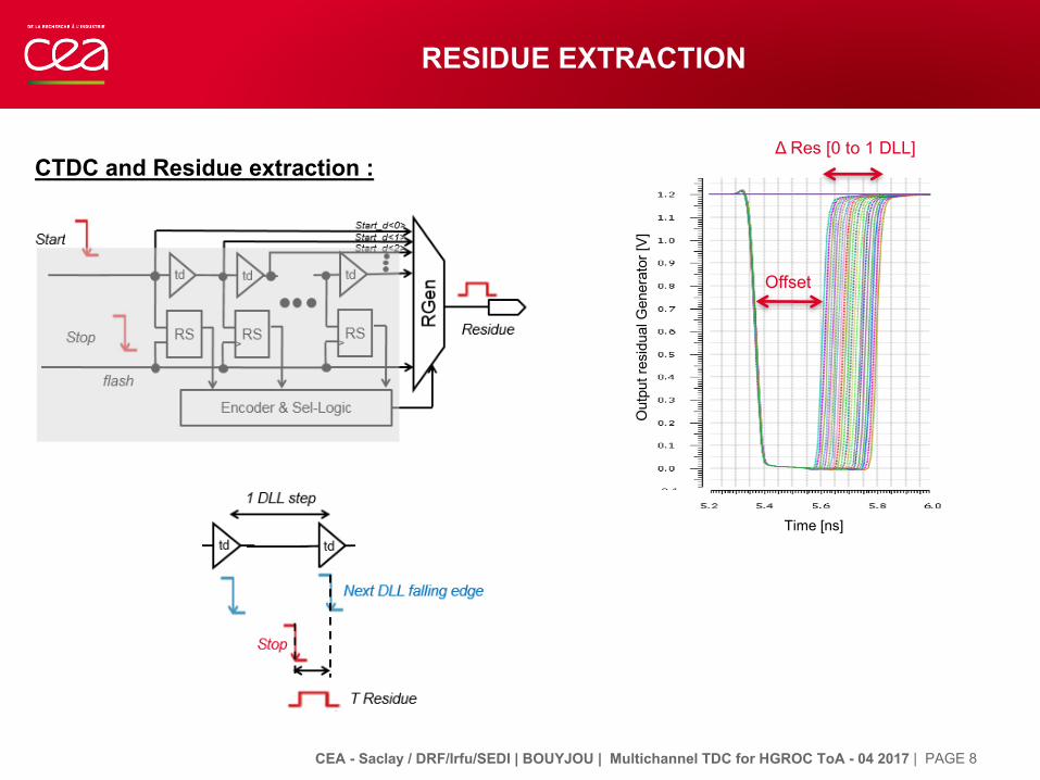
RESIDUE EXTRACTION
| PAGE 8CEA - Saclay / DRF/Irfu/SEDI | BOUYJOU | Multichannel TDC for HGROC ToA - 04 2017
CTDC and Residue extraction :Δ Res [0 to 1 DLL]
Out
put r
esid
ualG
ener
ator
[V]
Time [ns]
Offset

PULSE REPLICATOR
| PAGE 9CEA - Saclay / DRF/Irfu/SEDI | BOUYJOU | Multichannel TDC for HGROC ToA - 04 2017
Residue replication by 4, 8 or 16(programmable)
Out
put P
ulse
repl
icat
or [V
]
N×Residue
Copy frequency : 1,37 GHz
Total multiplication time :Gain x 8 : 6 nsGain x 16 : 12 ns
Pulse replicator :

FTDC : RESIDUE INTEGRATOR
| PAGE 10CEA - Saclay / DRF/Irfu/SEDI | BOUYJOU | Multichannel TDC for HGROC ToA - 04 2017
Counter : 0 1
195 ps
CTD
C a
nd F
TDC
[bits
]
3 FTDC bits
time of arrival START_TDC
5 CTDC bits
CTDC and FTDC ENCODER CODE evolution for different time of arrival Event between 2,6 and 3,4 ns and for CLK_PLL = 160 MHz
Pulse replicator + delay-line FTDC
Residue integrator :
FTDC = 𝑁. 𝑟𝑒𝑠𝑖𝑑𝑢𝑒
Warning : in this figure there is not enough simulated point to get a realistic estimation of the DNL and INL

TIME DOMAIN NOISE SIMULATION
CTDC residue NOISE histogram x10 Scale with START_TDC 2,85 ns and with PLL = 160 MHzExtracted with perfect input clock
CEA - Saclay / DRF/Irfu/SEDI | BOUYJOU | Multichannel TDC for HGROC ToA - 04 2017 | PAGE 11
FTD
C a
nd C
TDC
[bits
]Ti
me
Res
idue
[ps]
IterationStd Dev : 8,22/10 = 822 fs
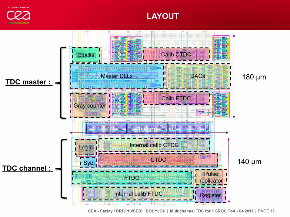
LAYOUT
| PAGE 12CEA - Saclay / DRF/Irfu/SEDI | BOUYJOU | Multichannel TDC for HGROC ToA - 04 2017
TDC channel :
TDC master :
Gray counter
Master DLLs
Clocks
Calib FTDC
Calib CTDC
DACs
Logic
Syc CTDC
FTDC
Internal calib CTDC
Internal calib FTDC
Pulse replicator
Register
180 µm
140 µm
310 µm

CONCLUSION
| PAGE 13CEA - Saclay / DRF/Irfu/SEDI | BOUYJOU | Multichannel TDC for HGROC ToA - 04 2017
Soumission en juin 2017.=> Rendez vous aux journées VLSI 2018 pour des résultats de mesure.
Time Of Arrival pour HGCAL
Type(s) de TDC(s) réalisé(s) Pulse train amplifier
Type d'intégration: ASIC ou FPGA ASIC
ASIC dédié TDC ou TDC intégré dans ASIC front-end TDC intégré dans ASIC front-end
Nombre de voie(s) 32 (64 ou 72 visés)
Technologie (pour les ASICs) TSMC 130nm
Gamme dynamique en temps 1,6 µsRésolution temporelle - Pas de quantification: simulés et mesurés 11 bits, LSB=12.5 ps Simulé.
Taux de comptage / temps mort individuel 40MHz (11 bits)
Consommation par voie 2mW. Ne consomme qu’en cas d’événement
Type de discriminateur utilisé, (selon) jitter, walk

PLL ARCHITECTURE
| PAGE 14CEA - Saclay / DRF/Irfu/SEDI | BOUYJOU | Multichannel TDC for HGROC ToA - 04 2017
• Multiplier : Generate 160 MHz from 40 MHz (have an 1.28 GHz output frequency for output)• Internal clock in phase with external 40 MHz (phase detector)• Cleaner : Reduce the jitter of the external 40 MHz (estimated at 25 ps) in order to have a
cleanest possible internal clock and less than the quantification noise of the TDC < 3.52 psMinimum and maximum lock frequencies : 21 to 47,6 MHz (BW : 20 MHz)
Architecture :
160, 320, 640 or 1280 MHz output
40 MHz input
RC-C filter
1,28 GHz Oscillator
32 pre-scaler
Phase detector :
External initial load voltage & adjustable current injection

TIME BUDGET
CEA - Saclay / DRF/Irfu/SEDI | BOUYJOU | CMS - 01 2017 | PAGE 15
Stop_K
Maximum 7,25 ns 3 bits x 0,73 ns = 5,84 ns4 bits x 0,73 ns = 11,68 ns
Maximum conversion time :10 bits TDC = 16 ns11 bits TDC = 22 ns
Mem + reset
= 3 ns
CTDC FTDC
Stop_ K SYNCHONISER
8 bits Register
TDC Channel K
VcompCoarse
TDCPulse
replicator
Stop_Coarse
5 bits Encoder
FineTDC
Stop_Fine
Residual replication
Residue
Start_Coarse
3/4 bits Encoder

TEMPERATURE AND PROCESS VARIATIONS
CEA - Saclay / DRF/Irfu/SEDI | BOUYJOU | Multichannel TDC for HGROC ToA - 04 2017 | PAGE 16
Internal DLL channel calibration :CTDC (Coarse TDC) and FTDC (Fine TDC) è Internalservo-controlled DLLTo have the same DLL time response according to the temperature and process variations
VD_CTDC_P & VD_FTDC_P internal calibration init to 0 V with VD_CTDC_N = 1,2 V and VD_FTDC_N = 1,2 V and VBIAS_N = 400 mV at -40, 0 and 40 °C [internal buffer]
VD_CTDC_P Final value at 10 µs VD_FTDC_P Final value > 20 µs
Initial lock DLL Calibration phase :
25 ns recalibration every 100 usto avoid the voltage node discharge (leakage current)
Commun master DLL for continuous calibration (mismatch?)
External initial load voltage & adjustable current injection

LAYOUT AND SIMULATION RESULTS
| PAGE 17CEA - Saclay / DRF/Irfu/SEDI | BOUYJOU | Multichannel TDC for HGROC ToA - 04 2017
TDC Simulation R&D TDCResolution 24.4 / 12.2 psBits 10 / 11 bits (over 25 ns)Rms noise ≈ 1 ps rmsConversion rate 10 bits TDC = 62,5 MHz
11 bits TDC = 45,6 MHzLinearity To be donePowerconsumption
During the conversion 2,18 mW [staticand dynamic] or 40 µW [static]
Calibration InternalArea 250 µm x 160 µmTechnology TSMC 130 nmTemperature -40 and 40 °C
PLL Simulation R&D PLLInput frequency 40 MHz (Bunch clock)Output frequecy MAX : 1.28 GHz
Output of intermediate frequencies :(640, 320, 160 MHz)
Jitter Jitter cleaner = 2.2 ps rmsCleaner 94 % (for 25 ps input jitter)
Power consumption 1.91 mWArea 515 µm x 141 µmTechnology TSMC 130 nmTemperature -40 and 40 °C
Area = 140 µm x 310 µmTriple wells under analog and digital
TDC layout :
Area = 515 µm x 141 µmTriple wells under analog and digital
PLL layout :

PLL TRANSIENT JITTER
| PAGE 18CEA - Saclay / DRF/Irfu/SEDI | BOUYJOU | Multichannel TDC for HGROC ToA - 04 2017
35 ps rms jitter noise added to perfect 40 MHz input clock (left) and the jitter of the 160 MHz output (right)
2.2 ps rms35 ps rms
40 MHz input 160 MHz output
Transient noise jitter injection with Cadence jitter source [extracted, buffer] @ 27 °C :
1400 periods :

DESIGN STATUT
| PAGE 19CEA - Saclay / DRF/Irfu/SEDI | BOUYJOU | Multichannel TDC for HGROC ToA - 04 2017
TDC StatutSchematics OKTemperature variation -40 to 40 °C OKMonte-Carlo (process & mismatch) -40 and 40 °C OKLayout OKExtracted view OKFine characterization process (INL, DNL, etc…) To be done
PLL StatutSchematics OKTemperature variation -40 to 40 °C OKMonte-Carlo (process & mismatch) -40 and 40 °C OKLayout OKExtracted view OKFine characterization process To be done
Next steps Statut32 Multi-channel TDC & PLL To be doneConnect the ToA TDC in HGROCv1 To be doneAdd internal slow control registers To be doneAdd internal references (DAC) To be donePAD, drivers connections, etc… To be doneDRC & LVS verifications To be doneFinal simulations To be done

DLL_CTDC & DLL_FTDC DELAYS
| PAGE 20CEA - Saclay / DRF/Irfu/SEDI | BOUYJOU | CMS - 01 2017
DLL_CTDC & DLL_FTDC delays with VD_P variations, VD_N = 1,2 V and at -40, 0 and 40 °C [parasitics included]
Simulation moderate Spectre APS ++aps NONE Preset
DLL_CTDC delay : 195 psVD_CTDC_P value = 612 mV
DLL_FTDC delay : 195 psVD_FTDC_P value = 745 mV

TOA PERFORMANCE
In testbeam : jitter = 500 ps/Q(fC) (+) 20 ps
In HGROC, simulated jitter = 1.2 ns/Q(fC)
VFE HGCAL - VIDYO MEETING - APRIL 18, 2017

GLOBAL ARCHITECTURE
CEA - Saclay / DRF/Irfu/SEDI | BOUYJOU | CMS - 01 2017 | PAGE 22
Clk 40 MHz
Discriminator
Counter
Channel K
TDC
CLK_160 MHz
PLL [osc 1,28 GHz]
RAM
Rst_counter
Input
2 bits counter min
Synccounter
CSA
CLK 1,28 GHz, 640 MHz, 320 MHz ?LVDS output
Enable
Mux Clk_selectExternal clk 160 MHz
Mux
External_IN_TDC_K
40 MHz internal
IN_select