team llamp nadja memic steve karcher sri teja basava francis yi laser lattice associative...
TRANSCRIPT
TEAM LLAMP
Nadja MemicSteve Karcher
Sri Teja BasavaFrancis Yi
Laser Lattice Associative Multi-touch Product
Preliminary Design Review
04/18/23 Department of Electrical & Computer Engineering 1
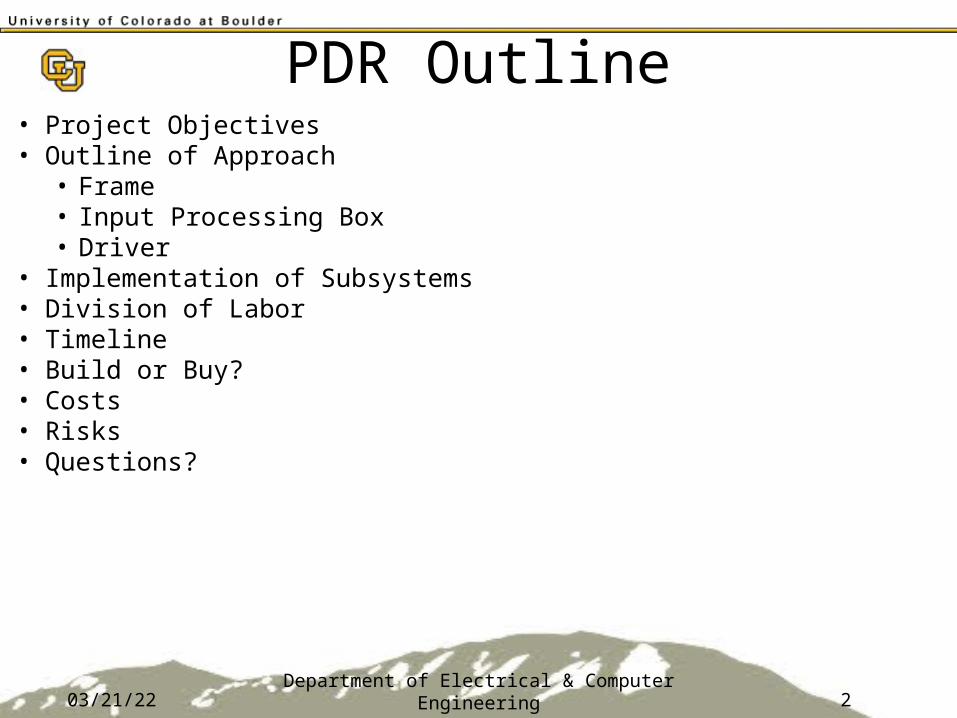
PDR Outline• Project Objectives• Outline of Approach
• Frame• Input Processing Box• Driver
• Implementation of Subsystems• Division of Labor• Timeline• Build or Buy?• Costs • Risks• Questions?
04/18/23 Department of Electrical & Computer Engineering 2

04/18/23 Department of Electrical & Computer Engineering 3
Project Objectives
04/18/23 Department of Electrical & Computer Engineering 4
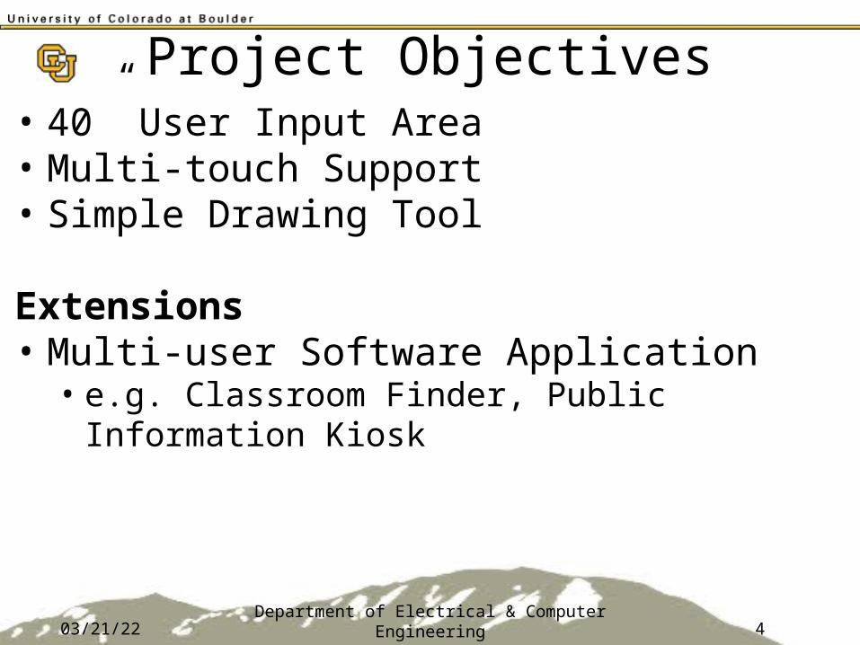
Project Objectives• 40” User Input Area• Multi-touch Support• Simple Drawing Tool
Extensions• Multi-user Software Application
• e.g. Classroom Finder, Public Information Kiosk
04/18/23 Department of Electrical & Computer Engineering 5
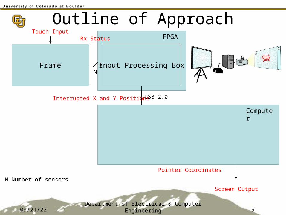
Outline of Approach
Frame Input Processing Box
DriverSoftware Application
(Drawing Tool)
USB 2.0
Touch Input
N
Interrupted X and Y Positions
Pointer Coordinates
Screen Output
FPGA
Computer
Rx Status
N Number of sensors
04/18/23 Department of Electrical & Computer Engineering 6
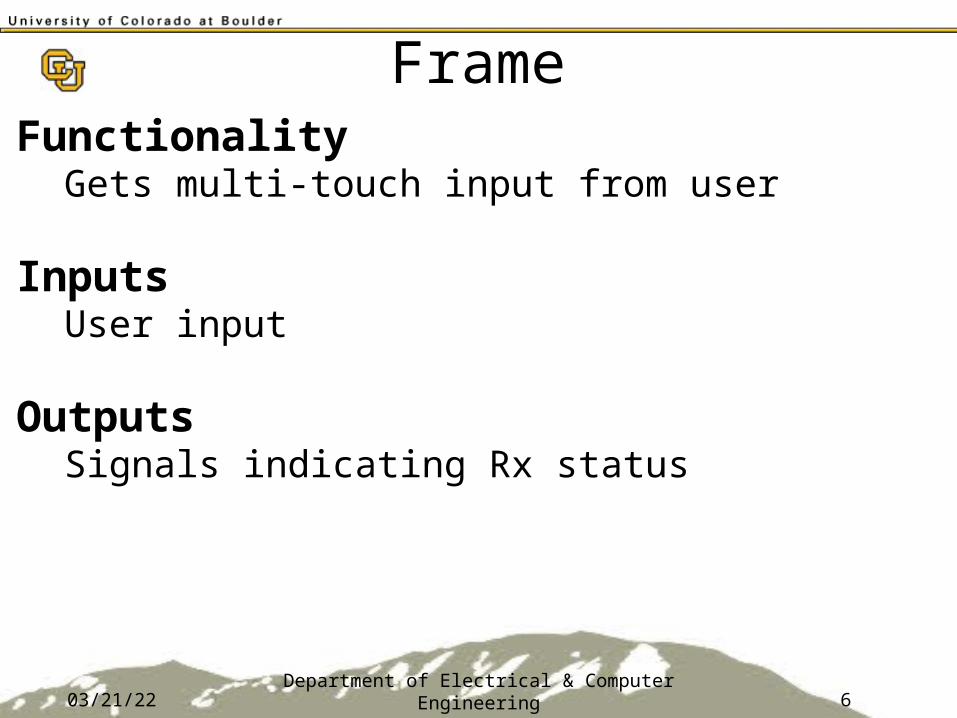
FrameFunctionality
Gets multi-touch input from user
InputsUser input
OutputsSignals indicating Rx status

04/18/23 Department of Electrical & Computer Engineering 7
Frame
40” Input Area
Tx
Tx…T
x
Tx …
Rx
Rx…
Rx
Rx …
Analog
Analog
+
-
VT
+
-
VT
Analog
Analog
+
-
VT
+
-
VT
Nx Number of horizontal Rx/TxNy Number of vertical Rx/TxVT Threshold Voltage
Nx
Nx
NyNy

04/18/23 Department of Electrical & Computer Engineering 8
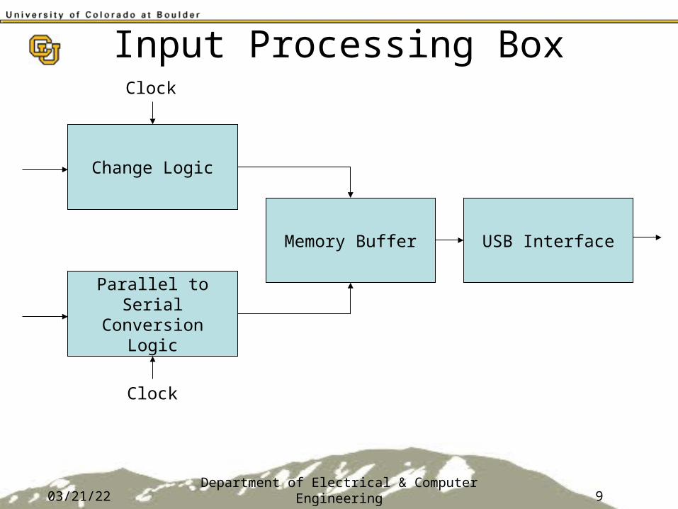
Input Processing Box• Functionality
• Processes and converts the interrupts for use by the driver
• Inputs• Signals indicating Rx status
• Outputs• Data indicating interrupted x and y positions
04/18/23 Department of Electrical & Computer Engineering 9
Input Processing Box
Change Logic
Parallel to Serial Conversion Logic
Memory Buffer
Clock
Clock
USB Interface

04/18/23 Department of Electrical & Computer Engineering 10
Driver• Functionality
• Gets the contents of memory buffer and interprets the x and y position data. This can then be used by the computer to control a mouse pointer.
• Inputs• Data indicating interrupted x and y positions from
memory buffer
• Outputs• Mouse control signal

04/18/23 Department of Electrical & Computer Engineering 11
Driver
Proximity Detection Module
Average Calculation Module
USB Driver

04/18/23 Department of Electrical & Computer Engineering
Implementation of Subsystems
Pictures from left to right from: http://www.knjn.com/ShopItemsPics/Board_Xylo-L.jpg, http://en.wikipedia.org/wiki/Image:Windowsloadingdrivers.jpg, http://www.publicdataweb.com/PDW/images/gif/Kiosk-BusStop-Anime.gif
12

04/18/23 Department of Electrical & Computer Engineering 13
Division of Labor and Responsibilities
1. Frame:
- Housing
- Circuitry/Board
- Tx/Rx Research
2. Input Processing Box:
- FPGA choice
- Logic algorithm development
- Adapting to our platform
3. Driver Development:
- Updating, averaging, proximity & toggling
4. Software Application:
- Implementation of painting ftn
Francis & Nadja
Steve & Teja
Entire Team
Steve & Teja
Francis, Nadja & Teja
Francis, Steve & Nadja
Teja & Francis
Entire Team

04/18/23 Department of Electrical & Computer Engineering 14
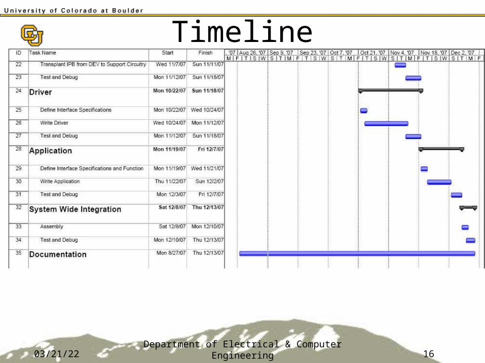
Timeline• User Input Area
Test and choose solutionGrid constructionChoose logic solutionInput processing boxDevelop on DEV board
• Write driver code
• Application
• System Wide Integration
Board Layout
Develop support circuitry
•Transplant DEV board

04/18/23 Department of Electrical & Computer Engineering 15
Timeline
04/18/23 Department of Electrical & Computer Engineering 16
Timeline
04/18/23 Department of Electrical & Computer Engineering 17
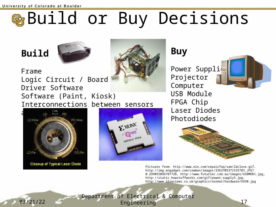
Build or Buy Decisions
Build
FrameLogic Circuit / Board LayoutDriver SoftwareSoftware (Paint, Kiosk)Interconnections between sensors and FPGA
Buy
Power SuppliesProjectorComputerUSB ModuleFPGA ChipLaser DiodesPhotodiodes
Pictures from: http://www.eio.com/repairfaq/sam/ldclose.gif, http://img.engadget.com/common/images/3363705371535783.JPG?0.299055096787738, http://www.futurlec.com.au/images/USBMOD1.jpg, http://static.howstuffworks.com/gif/power-supply5.jpg,http://www.itreviews.co.uk/graphics/normal/hardware/h930.jpg

04/18/23 Department of Electrical & Computer Engineering 18
Item $/unit # of units Total
Laser diode 2.50 100 $250.00
Photodiode 2.50 100 $250.00
Frame material 100.00 1 $100.00
Circuit board 66.00 4 $264.00
Power supply 60.00 1 $60.00
FPGA chip 80.00 1 $80.00
Miscellaneous $55.99
Grand Total: $999.99
Costs
Department of Electrical & Computer Engineering 19
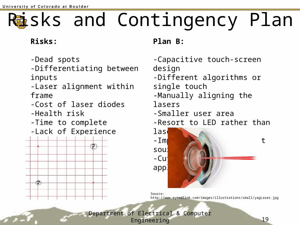
Risks and Contingency PlanRisks:
-Dead spots-Differentiating between inputs-Laser alignment within frame-Cost of laser diodes-Health risk-Time to complete-Lack of Experience
Plan B:
-Capacitive touch-screen design-Different algorithms or single touch-Manually aligning the lasers-Smaller user area-Resort to LED rather than lasers-Implement a weaker light source-Cut back on software applications
Source: http://www.eyemdlink.com/images/illustrations/small/yagLaser.jpg

Thank You!
Questions?
04/18/23 Department of Electrical & Computer Engineering 20
?