technical information thinpak 8x8
TRANSCRIPT

New High Voltage
SMD-Package
ThinPAK 8x8
April 2010
Version 1.0

Page 2April 2010
Introduction
Package Specification
Thermal Concept
Application Test Conditions
Impact on Efficiency and EMI
Switching behaviour
Portfolio and Target Applications
Standardization
Summary
Content
Page 3April 2010
ThinPAK 8x8 - Introduction
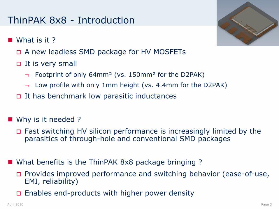
What is it ?
A new leadless SMD package for HV MOSFETs
It is very small
¬ Footprint of only 64mm² (vs. 150mm² for the D2PAK)
¬ Low profile with only 1mm height (vs. 4.4mm for the D2PAK)
It has benchmark low parasitic inductances
Why is it needed ?
Fast switching HV silicon performance is increasingly limited by the parasitics of through-hole and conventional SMD packages
What benefits is the ThinPAK 8x8 package bringing ?
Provides improved performance and switching behavior (ease-of-use, EMI, reliability)
Enables end-products with higher power density
Page 4April 2010
Introduction
Package Specification
Thermal Concept
Application Test Conditions
Impact on Efficiency and EMI
Switching behaviour
Portfolio and Target Applications
Standardization
Summary
Content

Page 5April 2010
Package specification
SMD package - leadless
Height: 1 mm package height
Footprint smaller than D2PAK (8 x 8 mm²)
Rdson -> similar to D²PAK / TO220
Creepage distance: 2.7 mm
Low Parasitics (package inductivity, package resistance)
Double sided cooling (optional)
Soldering: wave and reflow
Green mold compound
Page 6April 2010
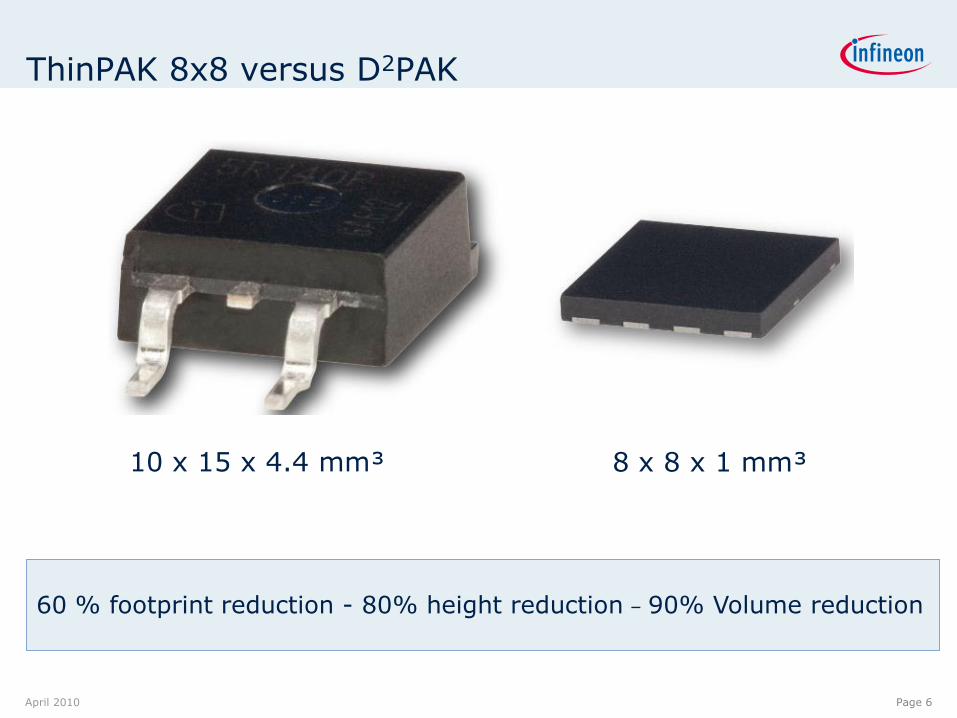
ThinPAK 8x8 versus D2PAK
10 x 15 x 4.4 mm³ 8 x 8 x 1 mm³
60 % footprint reduction - 80% height reduction – 90% Volume reduction
Page 7April 2010
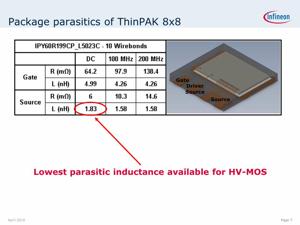
Package parasitics of ThinPAK 8x8
Driver Source
Source
Gate
Lowest parasitic inductance available for HV-MOS

Page 8April 2010
Gate driving circuit opportunity
Separate source connection for driver
¬ Negligible influence of the di/dt of the switched current
¬ Driver is able to provide a constant turn-on / turn-off voltage
Optimum performance can be achieved with
¬ Pulse transformer (primary side –main converter stage)
¬ Gate driving IC with separate power and signal GND
Driver Source
Source
Gate

Page 9April 2010
Gate driving circuit opportunity
Pulse transformer Driver with separated ground
Lsource
VIN
GND
DRV
GNDsignal
Signal-IN
GNDpower
Lsource
Pulse
Transformer
VIN
GND
V+
V-
Minimizing influence of the source inductance possible

Page 10April 2010
Content
Introduction
Package Specification
Thermal Concept
Application Test Conditions
Impact on Efficiency and EMI
Switching behaviour
Portfolio and Target Applications
Standardization
Summary

Page 11April 2010
Rth Junction to Ambient
Rth- Datasheet values
Thermal Resistance:Comparison D2PAK vs. ThinPAK 8x8
Product IPB60R199CP – D²PAK IPL60R199CP – ThinPAK 8x8
Rth-JC 0,9 K/W 0,9 K/W
Rth-JA 40 K/W 42 K/W
Page 12April 2010
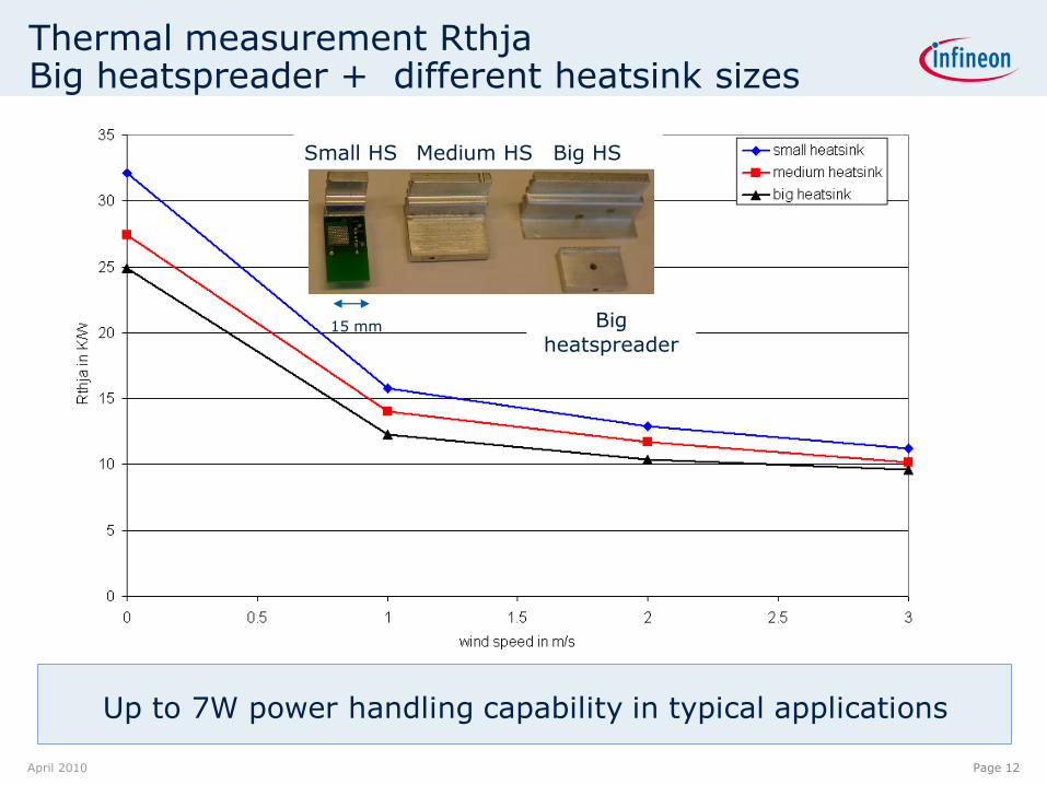
Thermal measurement RthjaBig heatspreader + different heatsink sizes
Small HS Medium HS Big HS
Big heatspreader
15 mm
Up to 7W power handling capability in typical applications
Page 13April 2010
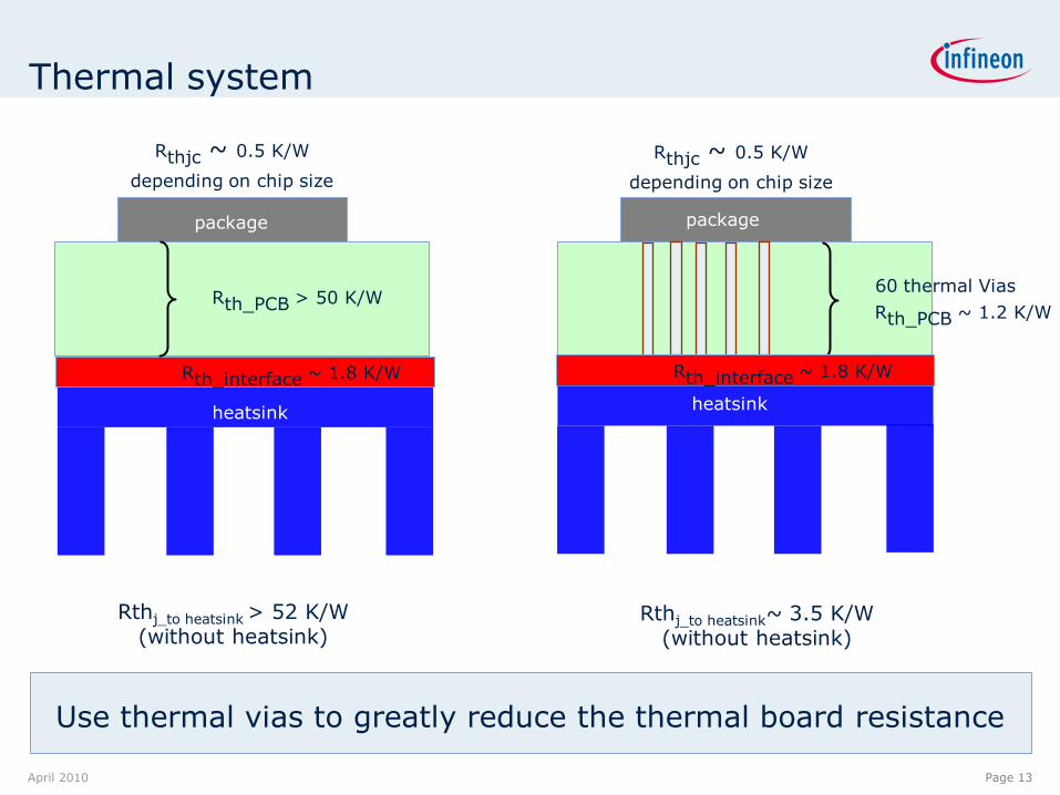
Thermal system
Rthjc ~ 0.5 K/W
depending on chip size
Rth_PCB > 50 K/W
Rth_interface ~ 1.8 K/W
Rthj_to heatsink > 52 K/W(without heatsink)
60 thermal Vias
Rth_PCB ~ 1.2 K/W
Rth_interface ~ 1.8 K/W
Rthj_to heatsink~ 3.5 K/W(without heatsink)
package package
Rthjc ~ 0.5 K/W
depending on chip size
heatsinkheatsink
Use thermal vias to greatly reduce the thermal board resistance

Page 14April 2010
Thermal PCB available solutions
2 layer PCB
Thermal vias for thermal coupling to heatsink
Multi layer PCB
Shifted thermal vias with heat spreading layer and EMI-shielding
PCB with Cu-inlay
Cu-Inlay for high thermal conductivity
Chip
Solder
Cu-inlay
Adhesive tape or glue
Heatsink

Page 15April 2010
Introduction
Package Specification
Thermal Concept
Application Test Conditions
Impact on Efficiency and EMI
Switching behaviour
Portfolio and Target Applications
Standardization
Summary
Content

Page 16April 2010
Application Test Conditions
Application CCM PFC
Max Output Power (W) 300W
PFC Controller ICE2PCS01G
PFC Diode 5A SiC
Heatsink Temperature 60oC
PCB PFC Adapter Board_2

Page 17April 2010
ThinPAK 8x8 adapter PCB for PFC stage
MOSFET199mOhm CP
SiC Diode2nd Gen 5A
Ceramic Cap500V 100n
Variable Rg
Ceramic Cap500V 10n
Gate driver IC
Connector array to PFC-Board
Application Test Condition
Page 18April 2010
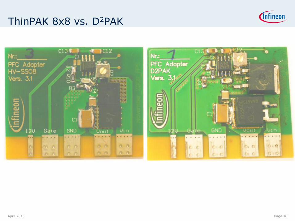
ThinPAK 8x8 vs. D2PAK
Page 19April 2010
GND
Vout
GND
Vin
C
Diode
MOSFET
Inductor
Bulk C
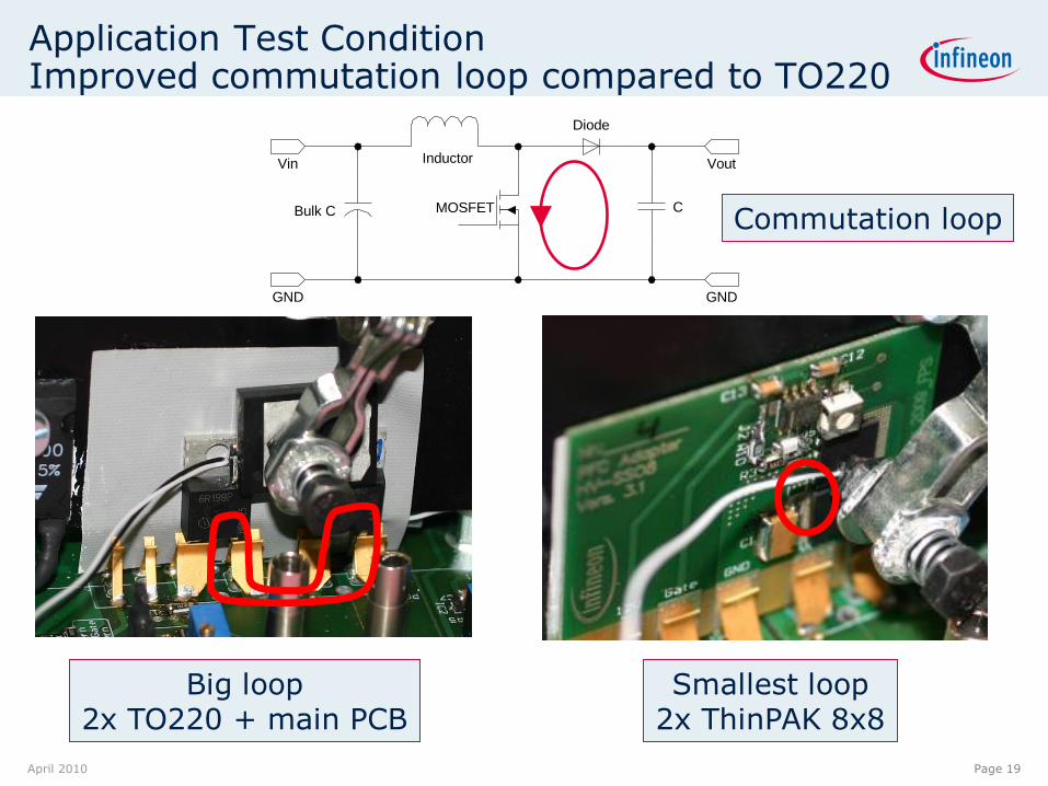
Application Test ConditionImproved commutation loop compared to TO220
Commutation loop
Big loop2x TO220 + main PCB
Smallest loop2x ThinPAK 8x8

Page 20April 2010
Content
Introduction
Package Specification
Thermal Concept
Application Test Conditions
Impact on Efficiency and EMI
Switching behaviour
Portfolio and Target Applications
Standardization
Summary
Page 21April 2010
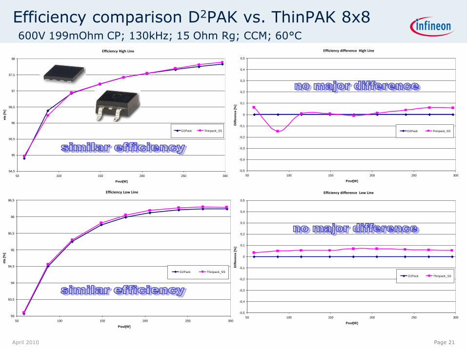
Efficiency High Line
94,5
95
95,5
96
96,5
97
97,5
98
50 100 150 200 250 300
Pout[W]
eta
[%
]
D2Pack Thinpack_SS
Efficiency comparison D2PAK vs. ThinPAK 8x8600V 199mOhm CP; 130kHz; 15 Ohm Rg; CCM; 60°C
Efficiency difference High Line
-0,5
-0,4
-0,3
-0,2
-0,1
0
0,1
0,2
0,3
0,4
0,5
50 100 150 200 250 300
Pout[W]
Dif
fere
nce [
%]
D2Pack Thinpack_SS
Efficiency Low Line
93
93,5
94
94,5
95
95,5
96
96,5
50 100 150 200 250 300
Pout[W]
eta
[%
]
D2Pack Thinpack_SS
Efficiency difference Low Line
-0,5
-0,4
-0,3
-0,2
-0,1
0
0,1
0,2
0,3
0,4
0,5
50 100 150 200 250 300
Pout[W]
Dif
fere
nce [
%]
D2Pack Thinpack_SS

Page 22April 2010
EMI Measurement 200W; 15 Ohm Rg, 130kHz
D2PAK (TO263)
ThinPAK 8x8

Page 23April 2010
Content
Introduction
Package Specification
Thermal Concept
Application Test Conditions
Impact on Efficiency and EMI
Switching behaviour
Portfolio and Target Applications
Standardization
Summary
Page 24April 2010
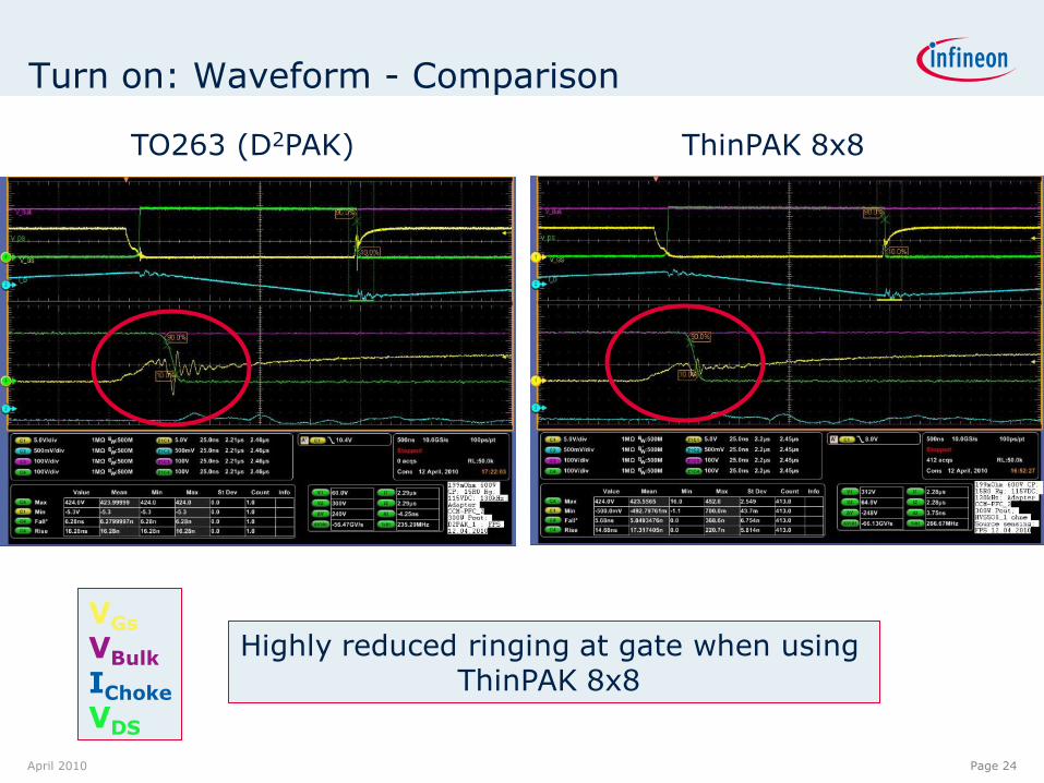
Turn on: Waveform - Comparison
TO263 (D2PAK) ThinPAK 8x8
Highly reduced ringing at gate when using ThinPAK 8x8
VGs
VBulk
IChoke
VDS

Page 25April 2010
Turn off: Waveform – Comparison
VGs
VBulk
IChoke
VDS
TO263 (D2PAK) ThinPAK 8x8
Highly reduced ringing at gate when using ThinPAK 8x8

Page 26April 2010
Waveforms – 50ms AC line drop out
VGs
VBulk
IChoke
VDS
Up to -12V on VGS
TO263 (DPAK)
ThinPAK 8x8
Up to -1,3V on VGS

Page 27April 2010
Content
Introduction
Package Specification
Thermal Concept
Application Test Conditions
Impact on Efficiency and EMI
Switching behaviour
Portfolio and Target Applications
Standardization
Summary
Page 28April 2010
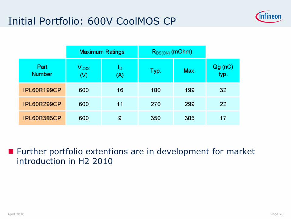
Initial Portfolio: 600V CoolMOS CP
Further portfolio extentions are in development for market introduction in H2 2010

Page 29April 2010
Target applications and topologies
Target applications:
Server (Computing, Telecom)
¬ CCM PFC, ITTF
High power density applications (e.g.: UPS)
Ultra slim adapter
¬ Quasi-resonant Fly-back
Lamp ballast HID applications
¬ DCM PFC
Daughter board use is a „new“ way to increase power density in compactness driven designs and target applications

Page 30April 2010
Content
Introduction
Package Specification
Thermal Concept
Application Test Conditions
Impact on Efficiency and EMI
Switching behaviour
Portfolio and Target Applications
Standardization
Summary

Page 31April 201031
Standardization is key in today´s market
Infineon & ST
Package footprint is supported by two major global power semiconductor suppliers
ThinPAK 8x8 PowerFLAT™ 8x8 HV
=

Page 32April 2010
Content
Introduction
Package Specification
Thermal Concept
Application Test Conditions
Impact on Efficiency and EMI
Switching behaviour
Portfolio and Target Applications
Standardization
Summary

Page 33April 2010
Summary of Advantages
Leadless SMD approach enables highest power density designs
Small footprint (64 mm² vs. 150 mm² for D2PAK)
Low profile package (1.0 mm vs. 4.4 mm for D2PAK)
Highly improved commutation loop (MOSFET, Diode, Cap)
Lowest stray inductances leads to lower VDS overshoots
Small Drain area
Smaller capacitive coupling of the Drain to the heat sink compared to TO220
Lowest Lsource (2 nH vs. 6 nH for D2PAK)
Separate driver source connection
Cleaner Waveforms, Easy to use for fast switching MOSFETs
Less tendency for dynamic re-turn-on or re-turn-off
Much easier for paralleling in high current applications
